US5457339A - Semiconductor device for element isolation and manufacturing method thereof - Google Patents

Semiconductor device for element isolation and manufacturing method thereof Download PDF

Info

Publication number
US5457339A
US5457339A US08/252,629 US25262994A US5457339A US 5457339 A US5457339 A US 5457339A US 25262994 A US25262994 A US 25262994A US 5457339 A US5457339 A US 5457339A
Authority
US
United States
Prior art keywords
trench
semiconductor device
substrate
element isolation
impurity concentration
Prior art date
Legal status (The legal status is an assumption and is not a legal conclusion. Google has not performed a legal analysis and makes no representation as to the accuracy of the status listed.)
Expired - Lifetime
Application number
US08/252,629
Inventor
Shigeki Komori
Katsuhiro Tsukamoto
Current Assignee (The listed assignees may be inaccurate. Google has not performed a legal analysis and makes no representation or warranty as to the accuracy of the list.)
Renesas Electronics Corp
Original Assignee
Mitsubishi Electric Corp
Priority date (The priority date is an assumption and is not a legal conclusion. Google has not performed a legal analysis and makes no representation as to the accuracy of the date listed.)
Filing date
Publication date
Priority claimed from JP04326457A external-priority patent/JP3092834B2/en
Application filed by Mitsubishi Electric Corp filed Critical Mitsubishi Electric Corp
Priority to US08/252,629 priority Critical patent/US5457339A/en
Application granted granted Critical
Publication of US5457339A publication Critical patent/US5457339A/en
Assigned to RENESAS ELECTRONICS CORPORATION reassignment RENESAS ELECTRONICS CORPORATION ASSIGNMENT OF ASSIGNORS INTEREST (SEE DOCUMENT FOR DETAILS). Assignors: MITSUBISHI DENKI KABUSHIKI KAISHA
Anticipated expiration legal-status Critical
Expired - Lifetime legal-status Critical Current

Links

Images

Classifications

    • HELECTRICITY
    • H01ELECTRIC ELEMENTS
    • H01LSEMICONDUCTOR DEVICES NOT COVERED BY CLASS H10
    • H01L21/00Processes or apparatus adapted for the manufacture or treatment of semiconductor or solid state devices or of parts thereof
    • H01L21/70Manufacture or treatment of devices consisting of a plurality of solid state components formed in or on a common substrate or of parts thereof; Manufacture of integrated circuit devices or of parts thereof
    • H01L21/71Manufacture of specific parts of devices defined in group H01L21/70
    • H01L21/76Making of isolation regions between components
    • H01L21/763Polycrystalline semiconductor regions

Definitions

  • the present invention relates to a semiconductor device for element isolation and to manufacturing method thereof. More particularly, the present invention relates to a semiconductor device for element isolation and manufacturing method thereof which allows fine element isolation.
  • LOCOS Local Oxidation of Silicon
  • a trench 31 is formed from a surface of p type semiconductor substrate 30 to a depth of about 1-2 ⁇ m.
  • a side surface of trench 31 is covered with an oxide film 34, and a P + type semiconductor layer 35 of a concentration of 10 20 -10 22 cm 3 is formed with oxide film 34 interposed.
  • P + type diffusion layer 36 of a concentration of 10 20 -10 22 cm 3 for preventing formation of an inversion layer in the surface of p type semiconductor substrate 30 is formed and serves as a channel stopper.
  • P + type diffusion layer 36 also serves to prevent a punch through phenomenon.
  • an oxide film 38 is formed in a thickness of about 1000-2000 ⁇ .
  • a gate oxide film 39 is formed on a surface of P type semiconductor substrate 30 except an area where oxide film 38 is formed.
  • a structure of a MOS transistor to which the structure for isolation is applied will be described hereinafter.
  • a gate electrode 40 is formed on gate oxide film 39 of the structure for isolation described above. Source/drain regions 41 of N + type impurity region are formed to a predetermined depth on both sides of gate electrode 40.
  • Gate electrode 40 is covered with interlayer insulating film 42.
  • a metallic interconnection 43 electrically connected to gate electrode 40 is formed to extend beneath interlayer insulating layer 42 above trench 31.
  • a thin thermal oxide film 32 having a thickness of about 300 ⁇ is formed on P type semiconductor substrate 30.
  • a nitride film 33 is grown by a CVD method, and regions of nitride film 33, oxide film 32 and semiconductor substrate 30 which are to be regions for isolation are etched to a depth of about 1-2 ⁇ m to form trench 31.
  • thermal oxide film 34 in the bottom portion of trench 31 is etched away by anisotropic etching to expose semiconductor substrate 30. Since a transistor forming region is covered with nitride film 33 which serves as a mask, etching of the region is prevented. Thereafter, a polycrystalline silicon 35 is grown to about 1-2 ⁇ m on the entire surface of the substrate including trench 31.
  • impurities of a p type conductivity which is the same as that of the substrate are introduced into polycrystalline silicon 35 at a high concentration by an ion implantation or a gas phase doping, and diffused so deeply as to reach semiconductor substrate 30 contacting polycrystalline silicon 35 at the bottom surface portion of trench 31 in heat treatment.
  • P + type diffusion layer 36 is then formed as a channel stopper in semiconductor substrate 30 under the bottom portion of trench 31. Since the transistor forming region is covered with nitride film 33, impurities are not diffused into the region. Also, the side surface of trench 31 is covered with thermal oxide film 34, and therefore impurities are not diffused thereto.
  • a photoresist film 37 is formed to flatten the surface of polycrystalline silicon 35.
  • Photoresist film 37 and polycrystalline silicon 35 having diffused impurities are etched back by anisotropic etching until the surface of nitride film 33 is exposed. As shown in FIG. 74, a structure in which polycrystalline silicon 35 fills trench 31 is thus finished. Thereafter, semiconductor substrate 30 is thermally oxidized and a relatively thin oxide film 38 is formed in a thickness of about 1000 ⁇ -2000 ⁇ on a surface of polycrystalline silicon 35 embedded in trench 31. Nitride film 33 and thermal oxide film 32 are removed, and a gate oxide film 39 is formed (FIG. 75). The structure for isolation is thus finished.
  • gate electrode 40 is patterned to a predetermined shape and source/drain regions 41 are formed.
  • Interlayer insulating film 42 is grown, a contact hole is opened at a predetermined position and metallic interconnection 43 is provided.
  • AMOS transistor as shown in FIG. 70 is then finished.
  • CMOS transistor having the structure for isolation of a semiconductor device will be described hereinbelow with reference to FIGS. 76 through 87.
  • phosphorus (P) is implanted to a predetermined depth in a left half region of p type semiconductor substrate 51 under conditions of 500 KeV-1.5 MeV and 1 ⁇ 10 12 -1 ⁇ 10 15 cm -2 .
  • Heat treatment is carried out for 20 minutes to 10 hours at temperature of 800°-1200° C. to form an n type impurity diffusion region 53.
  • n + impurity diffusion region 53 of p type semiconductor substrate 51 is covered with a resist film 54.
  • Boron (B) is implanted into a right half region of p type semiconductor substrate 51 under conditions of 200 KeV-1 MeV and 1 ⁇ 10 12 -1 ⁇ 10 15 cm -2 . Heat treatment is carried out for 20 minutes-10 hours at temperature of 800°-1200° C. to form a p type impurity diffusion region 55.
  • a thin thermal oxide film 56 of a thickness of about 300 ⁇ is formed on surfaces of n type impurity diffusion region 53 and p type impurity diffusion region 55 and a nitride film 57 is grown on oxide film 56 using the CVD method.
  • a resist film 58 is formed on nitride film 57 and is patterned.
  • regions of nitride film 57, oxide film 56, n type impurity diffusion region 53 and p type impurity diffusion region 55 which are to be an isolation region are etched to a depth of about 1-2 ⁇ m, so that trenches 59, 60 are formed as shown in FIG. 79.
  • thermal oxide films 61, 62 are formed relatively thick in trenches 59, 60.
  • Thermal oxide films 61, 62 on bottom surfaces of trenches 59, 60 are removed by anisotropic etching to expose semiconductor substrate 51.
  • n type impurity diffusion region 53 and p type impurity diffusion region 55 are not etched, since they are covered with nitride film 57 which serves as a mask.
  • a polycrystalline silicon 70 is grown to about 1-2 ⁇ m on the entire surface of semiconductor substrate 51 including trenches 59, 60.
  • a surface of polycrystalline silicon 70 above p type impurity diffusion region 55 is again covered with resist film 63, and phosphorus (P) is implanted into polycrystalline silicon 70 above n type impurity diffusion region 53 under conditions of 100 KeV and 1 ⁇ 10 12 -1 ⁇ 10 16 cm -2 .
  • a resist film 64 is formed on n + type impurity diffusion region 70a of a high concentration.
  • Boron (B) is implanted into polycrystalline silicon 70 above p type impurity diffusion region 55 under conditions of 50 KeV and 1 ⁇ 10 12 -1 ⁇ 10 16 cm -2 in the same manner as is described above.
  • photoresist film 65 is provided on surfaces of p + type impurity diffusion region 70a and n + type impurity diffusion region 70b to flatten these surfaces.
  • photoresist film 65, n + type impurity diffusion region 70a and p + type impurity diffusion region 70b are etched back, and nitride film 57 is exposed. Heat treatment is carried out under conditions of temperature of 800° C.-1200° C. and a time of 20 minutes-10 hours. Impurities in n type impurity diffusion region 70a and p + type impurity diffusion region 70b are diffused from bottom portions of trenches 59, 60, respectively to substrate 51.
  • n + type impurity diffusion region 70a and p + type impurity diffusion region 70b are embedded in trenches 59 and 60, respectively, and n diffusion layer 53a and p + diffusion layer 55a serving as channel stoppers exist in the bottom portions of these trenches.
  • a semiconductor substrate 51 is thermally oxidized, and relatively thin oxide films 66, 67 (about 1000-2000 ⁇ ) are formed on the surfaces of n + type impurity diffusion region 70a and p + type impurity diffusion region 70b embedded in trenches 59, 60. Thereafter, nitride film 57 and thermal oxide film 56 are removed and a gate oxide film 68 is formed.
  • a structure for isolation used for a CMOS is thus finished.
  • gate oxide film 80 is deposited and a gate electrode 81 is formed.
  • Gate electrode 81 is etched to have a predetermined shape using photolithography.
  • Source/drain regions 82, 83 are each formed in the substrate.
  • An interlayer oxide film 84 is deposited on the entire surface of the substrate.
  • Contact holes 85 reaching source/drain regions 82, 83 are opened using photolithography.
  • Aluminum 86 is deposited by sputtering and aluminum 86 is etched using photolithography. A CMOS transistor as shown in FIG. 87 is thus finished.
  • the p + semiconductor layer 35 has high impurity concentration in the range of 1 ⁇ 10 20 to 1 ⁇ 10 22 cm 3 . Therefore, when a gate electrode is formed on the oxide film 38 as shown in the figure, a capacitor C 1 having a large parasitic capacitance is formed by the gate electrode 40, the oxide film 38 and the p + semiconductor layer 35.
  • the existence of the capacitor C1 represented in an equivalent circuit is as shown in FIG. 89.
  • the capacitor C 1 exists, electrons are charged/discharged to and from the capacitor C 1 on the output side (OUT) of the circuit, which causes delay in signals. Therefore, as shown in the graph of FIG. 90, the speed of the device becomes slower.
  • the semiconductor layer 35 comes to have a nature near an insulator. Therefore, as shown in FIG. 91, the electric field E from the gate electrode 4 inverts the sidewalls of the trench 31 directly, causing degradation of isolation.
  • An object of the present invention is to provide a semiconductor device for element isolation having a structure for isolation in a form of a trench without a need of a channel stopper region.
  • Another object of the present invention is to provide a manufacturing method of a semiconductor device for element isolation in which impurities are implanted and diffused into a substrate such that a band of maximum impurity concentration is positioned at a predetermined depth in the substrate.
  • a still further object of the present invention is to provide a semiconductor device for element isolation superior in element isolation and having highly reliable element isolating structure and to provide a manufacturing method thereof.
  • the semiconductor substrate has a main surface.
  • the semiconductor substrate has a band of maximum impurity concentration of impurities of a first conductivity type at a prescribed depth from and approximately parallel to the main surface.
  • the semiconductor substrate has lower impurity concentration between the main surface and the band of the maximum impurity concentration.
  • a trench for isolation has a sidewall extending from the main surface to the band of the maximum impurity concentration, which trench for isolation is filled with an isolating material.
  • a uniform p + high concentration region is substantially formed in the bottom portion of the isolation region, so that an isolation threshold value is not affected. Also, as to isolation breakdown voltage and anti-punch through property, a depletion layer from source/drain regions do not join because of the existence of the uniform p + high concentration region, and therefore a punch through phenomenon can be effectively suppressed.
  • a semiconductor device for element isolation for achieving the above-stated objects includes a semiconductor substrate having a first conductivity type impurity region whose impurity concentration attains the maximum at a predetermined depth from a surface in the depth direction; a trench formed from the surface of the semiconductor substrate to a predetermined depth in the impurity region of the first conductivity type; an impurity diffusion region of the first conductivity type provided in the trench with a space from the sidewall, having only its bottom portion in contact with the above-mentioned impurity region of the first conductivity type in the semiconductor substrate and having almost the same impurity concentration as the aforementioned impurity region of the first conductivity type; an oxide film covering an upper surface of the impurity diffusion region and the surface of the semiconductor substrate as well as filling the space between the internal sidewall of the trench and the impurity diffusion region.
  • the semiconductor device for element isolation at first oxide films are provided on the sidewall portions of the trench as the isolating material provided in the trench.
  • a semiconductor layer is provided inside the oxide films provided on the sidewalls of the trench.
  • a trench is formed from a the main surface to a prescribed depth of a semiconductor substrate.
  • An isolating material is provided in the trench.
  • Impurities are introduced to the semiconductor substrate such that a band of a maximum impurity concentration exists approximately parallel to the main surface and at a prescribed depth from the main surface. Lower impurity concentration exists between the band of the maximum impurity concentration and the main surface, and the depth of the trench extends to the band of the maximum impurity concentration.
  • a manufacturing method of a semiconductor device for element isolation for achieving the above-stated objects includes the steps of forming a trench having a predetermined depth in a semiconductor substrate; forming an oxide film on an internal surface except a bottom surface of the trench; depositing a semiconductor layer in the trench; implanting and diffusing impurities of a first conductivity type into the semiconductor substrate and the semiconductor layer such that impurity concentration attains the maximum at a depth of the bottom of the trench in the depth direction.
  • the number of impurity implantation steps can be decreased, whereby the number of steps of forming resist films is also decreased.
  • a manufacturing process of a semiconductor device can be shortened.
  • the semiconductor device for element isolation of the present invention includes, in order to attain the above described objects, a semiconductor substrate having a main surface, a trench formed to a prescribed depth from the main surface, a pair of sidewall insulating films provided on the sidewalls of the trench, a buried layer having a prescribed impurity concentration buried in the trench surrounded by the pair of sidewall insulating films, an upper insulating film formed to cover the opening portion of the trench at the main surface, and a pair of conductive layers having higher impurity concentration than the buried layer formed at the side portions of the buried layer and in contact with the lower surface of the upper insulating film and in contact with inner surface of each of the sidewall insulating films.
  • the method of manufacturing a semiconductor device for element isolation of the present invention includes the following steps.
  • a trench having a prescribed depth is formed at the semiconductor substrate. Then, sidewall insulating films are formed on the sidewalls of the trench.
  • a conductive layer having a prescribed impurity concentration is formed in contact with the inner walls of the sidewall insulating films, from the main surface of the semiconductor substrate to a prescribed depth in the trench. Thereafter, a buried layer having impurity concentration lower than the conductive layer is formed in the trench surrounded by the conductive layer and by the sidewall insulating films.
  • an upper insulating film having a prescribed thickness covering the opening portion of the trench is formed at the surface of the buried layer.
  • a pair of conductive layers in contact with inner surfaces of the sidewall insulating films and in contact with the lower surface of the upper insulating film, provided near the side portions of the buried layer and having higher impurity concentration than the buried layer are provided. Consequently, impurity concentration of the buried layer as a whole can be set lower, which suppresses increase of parasitic capacitance. Since the conductive layer for the electric field from the gate electrode is provided, formation of inverted layer at the sidewall portions of the trench can be suppressed with the electric field suppressed by the conductive layer.
  • FIG. 1 is a cross section showing a structure of a semiconductor device for element isolation in accordance with a first embodiment of the present invention.
  • FIG. 2 is a cross sectional view showing another structure of the semiconductor device for element isolation in accordance with the first embodiment of present invention.
  • FIG. 3 (a) is a schematic diagram showing the separation threshold value
  • FIG. 3 (b) shows relation between voltage and current.
  • FIG. 4 (a) is a schematic diagram showing separation breakdown voltage
  • FIG. 4 (b) shows relation between the voltage and the current.
  • FIG. 5 is a diagram for comparing the separation threshold value in (a) LOCOS structure, (b) conventional structure and (c) the present embodiment.
  • FIG. 6 is a diagram for comparing separation breakdown voltage in (a) LOCOS structure, (b) conventional structure and (c) in the present embodiment.
  • FIG. 7 is a graph for obtaining set mixing ratio for making the each rate of silicon equal to the etch rate of resist.
  • FIGS. 8 to 18 are cross sections showing the first to eleventh steps of manufacturing in accordance with the first embodiment of the present invention.
  • FIG. 19 shows concentration distribution in the substrate when boron is implanted to the substrate at a prescribed energy and a prescribed concentration.
  • FIGS. 20 through 34 are cross sections showing the first to fifteenth steps of manufacturing a CMOS transistor in accordance with the present invention.
  • FIG. 35 is cross section showing a structure of a semiconductor device in accordance with a second embodiment of the present invention.
  • FIG. 36 is a schematic diagram showing operation principal of the structure shown in FIG. 35.
  • FIG. 37 shows relation between time and voltage showing the effect provided by the structure of FIG. 35.
  • FIG. 38 is a schematic diagram showing another effect provided by the structure shown in FIG. 35.
  • FIG. 39 shows relation between the gate voltage and the drain current showing the effect provided by the structure of FIG. 35.
  • FIGS. 40 to 50 are cross sections showing the first to eleventh steps of manufacturing in accordance with the second embodiment of the present invention.
  • FIG. 51 is a cross section showing a structure of a semiconductor device in accordance with a third embodiment of the present invention.
  • FIGS. 52 to 59 are cross sections showing the first to eighth steps of manufacturing in accordance with the third embodiment of the present invention.
  • FIG. 60 is a cross section showing another structure of the semiconductor device in accordance with the third embodiment of the present invention.
  • FIG. 61 is a cross section showing a structure of a semiconductor device in accordance with a fourth embodiment of the present invention.
  • FIGS. 62 to 69 are cross sections showing the first to eighth steps of manufacturing in accordance with the first embodiment of the present invention.
  • FIG. 70 is a cross section of a conventional semiconductor device.
  • FIGS. 71 to 75 are cross sections showing the first to fifth steeps of manufacturing the conventional semiconductor device.
  • FIGS. 76 to 87 show the first to twelfth steps of manufacturing a conventional CMOS transistor.
  • FIG. 88 is a cross section of a conventional semiconductor device.
  • FIG. 89 is an equivalent circuit diagram showing problems of a conventional element isolating structure.
  • FIG. 90 shows relation between time and voltage in the conventional structure.
  • FIG. 91 is a first schematic diagram showing a problem of the element isolating structure of the prior art.
  • FIG. 92 is a schematic diagram showing impurity diffusion during thermal processing in the conventional semiconductor device structure.
  • FIG. 93(a) is a schematic diagram showing impurity diffusion when the channel is wide in the structure of a conventional semiconductor device
  • FIG. 93(b) is a schematic diagram showing increase of concentration because of overlapped impurities when the channel is narrow in the structure of the conventional semiconductor device.
  • FIGS. 1 through 18 A semiconductor device and a manufacturing method according to a first embodiment of the present invention will be described hereinbelow with reference to FIGS. 1 through 18.
  • a structure of the semiconductor device includes a semiconductor substrate 1 including an impurity region 1a of a first conductivity type, for example, a p type whose impurity concentration attains the maximum at a predetermined depth from the surface, and a trench 6 formed from a surface of p type impurity region 1a of semiconductor substrate 1 to a predetermined depth in p type impurity region 1a.
  • a p type impurity diffusion region 8 is provided with a space from an internal sidewall, having only its bottom surface in contact with semiconductor substrate 1 and having almost the same concentration as impurity region 1a.
  • An oxide film 11 is formed to fill the space between the internal sidewall of trench 6 and p type impurity diffusion region 8 and to cover an upper surface of impurity diffusion region 8 and the surface of semiconductor substrate 1.
  • FIG. 2 another structure will be described.
  • the inside of the trench 6 is entirely filled by an oxide film.
  • cracks are generated in the oxide film during the step of thermal processing, since the difference of the coefficient of thermal expansion between the semiconductor substrate 1 and the oxide film 11 is large. If a crack is generated in the oxide film, a leak current is generated in the semiconductor substrate, degrading the capability of element isolation. Therefore, a structure relaxing the difference of the coefficient of thermal expansion by the provision of the semiconductor layer in the trench such as shown in FIG. 1 is preferred.
  • the structure shown in FIG. 1 is described in the following.
  • a gate electrode 7 is formed on an upper surface of oxide film 11 and source/drain regions 9, 10 of n + type impurity regions are formed to a predetermined depth in impurity region 1a on both sides of gate electrode 7.
  • isolation capability As to the isolation capability, both “an isolation threshold value” and “an isolation breakdown voltage” should be considered.
  • an isolation threshold value means a value of a gate voltage V g at which left and right source/drain regions 100, 101 are rendered conductive.
  • an isolation breakdown voltage is a voltage applied to one of source/drain regions 100, 101 when source/drain regions 100, 101 are rendered conductive or a junction breakdown occurs.
  • FIG. 4 (b) shows in the relationship between voltage Vd and current Id.
  • Isolation threshold values and isolation breakdown voltages of an LOCOS structure are compared for isolation capability.
  • a path between elements 100, 101 is long, as in the conventional structure, inversion in regions marked with X in the sidewall portion of the trench does not occur and therefore it is not easily rendered conductive. Also, since p + layer 103 of a high concentration is provided in the bottom portion of the trench, even if an inversion layer is formed, it is impossible to be rendered conductive and therefore isolation capability can be fully enhanced.
  • p + layer 103 can be substantially formed in the bottom portion of the substrate.
  • depletion layers from the source/drain regions are not joined because of the existence of p + layer 110, a punch through phenomenon can be effectively suppressed.
  • isolation can be achieved without providing a channel stopper region in a bottom portion of an isolation region.
  • a first oxide film 2 of SiO 2 is formed in a thickness of about 300 ⁇ on a surface of a semiconductor substrate 1 using a thermal oxidation method.
  • a first semiconductor layer 3 of polysilicon is formed in a thickness of about 500-2000 ⁇ on a surface of first oxide film 2 using the CVD method, and thereafter, a second oxide film 4 of SiO 2 is formed in a thickness of about 300 ⁇ on a surface of first semiconductor layer 3 using a thermal oxidation method.
  • a resist film 5 having a predetermined pattern is formed on a surface of second oxide film 4.
  • a trench 6 having a depth of about 0.3-1.0 ⁇ m is formed by anisotropic etching, using resist film 5 as a mask.
  • oxide film 11 is hereinafter referred to as an oxide film 11 hereinafter.
  • oxide film 11 in a bottom surface portion of trench 6 is etched away by anisotropic etching, so that semiconductor substrate 1 is exposed.
  • a second semiconductor layer 8 is epitaxially grown at a growth rate of 0.2-1.4 ⁇ m/min and at growth temperatures in a range of about 700° C. to 1200° C., using a gas such as SiCl 4 , SiHCl 3 , SiH 2 Cl 2 , SiH 4 in trench 6 and on a surface of oxide film 11.
  • a resist film 91 is formed flat on the surface of semiconductor layer 8 and etched back to a predetermined depth.
  • CCl 4 and O 2 are mixed such that an etch rate for silicon and an etch rate for resist are equal.
  • semiconductor layer 8 is thermally oxidized more deeply than the surface of semiconductor substrate 1, and oxide film 12 is formed.
  • Oxide film 11 and oxide film 12 are etched until a surface of semiconductor layer 3 is exposed. Referring to FIG. 17, only the exposed semiconductor layer 3 is etched away.
  • impurities of one conductivity type for example, boron (B) are simultaneously implanted and activated in semiconductor substrate 1 and second semiconductor layer 8 at a constant energy value in a range of 200 KeV-1 MeV and at a constant implantation amount in a range of 1 ⁇ 10 12 -1 ⁇ 10 15 cm -2 .
  • impurity concentration attains the maximum at depths of about 1.7 ( ⁇ m), 2.8 ( ⁇ m) and 4.0 ( ⁇ m), respectively, as shown in FIG. 19.
  • Semiconductor layer 8 forms an impurity diffusion region 8a. An isolation region of the semiconductor device in this embodiment is then finished.
  • the number of implantation steps of impurity regions is decreased by employing the isolation structure without a channel stopper as described above. Therefore, the number of steps of forming resist films can be decreased and thus the manufacturing process can be shortened.
  • a first oxide film 14 of SiO 2 is formed at a thickness of about 30 ⁇ on a surface of a semiconductor substrate 13 using a thermal oxidation method.
  • a first semiconductor layer 15 of polysilicon is formed in a thickness of about 500-2000 ⁇ on a surface of first oxide film 14 using a CVD method.
  • a second oxide film 16 of SiO 2 is formed in a thickness of about 300 ⁇ on a surface of first semiconductor layer 15.
  • a resist film 17 having a pattern for formation of an isolation trench is formed on a surface of second oxide film 16.
  • trenches 18, 19 having a depth of about 0.3-1.0 ⁇ m are formed using anisotropic etching.
  • oxide films are formed on internal surfaces of trenches 18, 19. At this time, first semiconductor layer 15 is further oxidized and a second oxide film 16 is thickened. In side surface portions of trenches 18, 19, second oxide film 16 and first oxide film 14 are united. An oxide film thus formed is hereinafter referred to as an oxide film 20.
  • oxide film 20 in a bottom surface portions of trenches 18, 19 is etched by anisotropic etching and semiconductor substrate 13 is exposed.
  • a second semiconductor layer 21 is formed in a thickness of about 0.1 ⁇ m by epitaxial growth, in trenches 18, 19 and on a surface of oxide film 20 using a gas such as SiCl 4 , SiHCl 3 , SiH 2 Cl 2 and SiH 4 at a growth rate of about 0.2-1.5 ⁇ m/min and grown temperatures in a range of 700° C. to 1200° C.
  • a resist film 22 is formed flat on a surface of semiconductor layer 21 and etched back to a predetermined depth.
  • CCl 4 for etching semiconductor layer 21 is mixed with O 2 for etching resist film 22 such that both etching rates are equal.
  • impurities are thermally diffused more deeply than a surface of semiconductor substrate 1 in semiconductor layer 21, and an oxide film 23 is formed.
  • Oxide film 20 and oxide film 23 are etched until a surface of semiconductor layer 15 is exposed. Referring to FIG. 30, only the exposed semiconductor layer 15 is etched away.
  • a resist film 25 is formed on a right half surface of oxide film 20.
  • phosphorus (P) is implanted at a constant energy values in a range of 500 KeV-1.5 MeV and at a constant implantation amount in a range of 1 ⁇ 10 12 -1 ⁇ 10 15 cm -2 .
  • Thermal diffusion is carried out at a temperature of 800°-1200° C. for 20 minutes-10 hours to form an n type diffusion impurity region 26 whose impurity concentration attains the maximum in a bottom portion of the substrate.
  • phosphorus (P) is simultaneously implanted and diffused in second semiconductor layer 21 formed in trench 18, and an n type impurity diffusion layer 21a is formed.
  • a resist film 27 is formed on a left half surface of oxide film 20 in the same manner as is described above.
  • boron (B) is implanted and diffused to a predetermined depth in a right half of semiconductor substrate 13, and a p type impurity diffusion region 28 is formed.
  • boron (B) is also implanted into a second semiconductor device 21 formed in trench 19 under conditions of respective constant values in a range of 200 KeV-1 MeV and 1 ⁇ 10 12 -1 ⁇ 10 15 cm -2 .
  • Thermal diffusion is carried out at a temperature of 800°-1200° C. for 20 minutes-10 hours and p type impurity diffusion layer 21b is then formed whose impurity concentration attains the maximum in a bottom portion of the substrate.
  • Resist film 27 is removed, so that an isolation region used for a CMOS transistor as shown in FIG. 33 is finished.
  • gate oxide film 11 is deposited and gate electrode 7 is formed.
  • Gate electrode 7 is etched to a predetermined shape using photolithography.
  • Source/drain regions 9, 10 are formed in respective wells.
  • An interlayer oxide film 24 is deposited on the whole surface of the substrate. Contact holes 24a reaching source/drain regions 9, 10 are opened using photolithography.
  • Aluminum 29 is deposited by sputtering and etched by photolithography.
  • An CMOS transistor as shown in FIG. 34 is then finished.
  • an epitaxial layer is formed to form the p type impurity diffusion region in the second semiconductor layer formed in the trench
  • metallic material of tungsten (W) may be deposited instead.
  • a mixed gas of Wf 6 and SiH 4 , or Wf 6 and H 2 is used at temperatures in range of about 400°-1000° C. in the CVD method.
  • the number of implantation steps of impurities is decreased, the number of steps of forming resist films is decreased to a half, so that the number of manufacturing steps can be decreased.
  • a trench 506 is formed to have the depth of about 1 to 2 ⁇ from the main surface of a p type semiconductor substrate 501.
  • a pair of sidewall insulating films 562 and 562 of oxide films are formed on the sidewalls of the trench 506.
  • a buried layer 510 having the impurity concentration in the range of 1 ⁇ 10 14 to 1 ⁇ 10 17 cm -3 is provided.
  • the buried layer 510 has a two layered structure including a lower buried layer 510a and an upper buried layer 510b.
  • the upper opening portion of the trench 506 is covered by an upper insulating film 503 of an oxide film.
  • a pair of conductive layers 520 and 520 having the impurity concentration of about 1 ⁇ 10 18 to 1 ⁇ 10 21 cm -3 are provided in contact with the lower surface of the upper insulating film 503 and inner surfaces of the sidewall insulating films 562 and near the side portions of the buried layer are provided.
  • the depletion layer 540 is formed entirely over the upper region of the buried layer 510. Therefore, the parasitic capacitance of the capacitor formed by the gate electrode 530, the upper electrode 503 and the buried layer 510 can be reduced. Consequently, speed of operation of the device isolated by this element isolating structure can be improved as shown in FIG. 37.
  • the electric field E from the gate electrode 530 the electric field E can be shielded by the conductive layers 520, as shown in FIG. 38. Therefore, the conductive layer 520 prevents inversion of the semiconductor substrate 501 at the edge portion of the trench 506. Thus the parasitic component of the transistor is cut, and a phenomenon in which the channel is not completely turned OFF can be prevented as shown in FIG. 39, allowing reduction of power.
  • FIGS. 40 to 50 are cross sections in accordance with the cross sectional structure shown in FIG. 35.
  • a first oxide film 551 of SiO 2 is formed to have the thickness of about 300 ⁇ by thermal oxidation on the surface of the semiconductor substrate 501.
  • a silicon nitride film 552 is formed by the CVD method to the thickness of about 2000 ⁇ on the surface of the first oxide film 551.
  • a second oxide film 553 of SiO 2 is formed to the thickness of about 2000 ⁇ by thermal oxidation on the silicon nitride film 512.
  • a resist film having a prescribed pattern (not shown) is formed on the second oxide film 513. Thereafter, by using the resist film as a mask, a trench 506 having the depth of about 0.3 to 1.0 ⁇ is formed by an isotropic etching.
  • the resist film is removed, and an oxide film 562 having the thickness of about 300 ⁇ is formed on the inner surface of the trench 506 by thermal oxidation. Thereafter, referring to FIG. 42, the oxide film 562 formed at the bottom portion of the trench 506 only is removed by anisotropic etching.
  • a polysilicon having the low impurity concentration of about 1 ⁇ 10 14 cm -3 is deposited by the CVD method on the entire surface of the substrate. Then, referring to FIG. 44, the polysilicon layer 55 is etched back to lead the polysilicon layer 554 at a prescribed region at the bottom of the trench 506 only, to form the lower buried layer 510a.
  • a high concentration polysilicon 512 having the impurity concentration of 1 ⁇ 10 18 cm -3 or higher is formed on the entire surface of the substrate by the CVD method, to the thickness of about 200 to 3000 ⁇ .
  • the high concentration polysilicon layer 512 has the same conductivity as the substrate, and in this embodiment, it has p type conductivity.
  • the polysilicon layer 512 formed at the upper portion of the lower buried layer 510a is removed by anisotropic etching.
  • the polysilicon layer 522 is etched back.
  • an upper buried layer 510b is formed in the trench 506.
  • the second oxide film 553 shown in FIG. 48 is removed by etching.
  • an upper insulating film 503 is formed by using the silicon nitride film 553 as a mask by a method similar to the conventional LOCOS method, by thermal oxidation.
  • the silicon nitride film 553 is removed by wet etching using phosphoric acid, and the element isolation structure shown in FIG. 35 is thus completed.
  • a pair of conductive layers having higher impurity concentration than the buried layer are provided near the side portions of the buried layer and in contact with the lower surface of the upper insulating film and in contact with the inner surfaces of the sidewall insulating films.
  • the impurity concentration of the buried layer as a whole can be set lower, suppressing parasitic resistance.
  • the electric field from the gate electrode the electric field is suppressed by the conductive layers and thus formation of inverted layer at the sidewall portions of the trench can be prevented.
  • the element isolating structure of the third embodiment differs from the structure of the second embodiment described above in the following points.
  • the conductive layers 520 and 520 are formed to the bottom of the trench 506. At the bottom of the trench 506, a bottom conductive layer 522 is formed.
  • the buried layer 510 is entirely formed of polysilicon layer of low impurity concentration.
  • the impurity concentration of the buried layer 510 As to the impurity concentration of the buried layer 510 as a whole, it should preferably be low in view of parasitic capacitance. Therefore, the ratio of the buried layer 510 occupied by the conductive layer 522 should be as small as possible.
  • the third embodiment is made to solve the above described the problem of the second embodiment.
  • FIGS. 52 to 59 are cross sections in accordance with the cross sectional structure shown in FIG. 51.
  • a first oxide film 551 of SiO 2 is formed to the thickness of 300 ⁇ by thermal oxidation on the surface of the semiconductor substrate 501.
  • a silicon nitride film 552 having the thickness of about 2000 ⁇ is formed on the surface of the first oxide film 551.
  • a second oxide film 553 is formed to the thickness of about 2000 ⁇ by thermal oxidation on the silicon nitride film 552.
  • a resist film having a prescribed pattern (not shown) is formed on the second oxide film 553. Thereafter, by using the resist film as a mask, a trench 506 having the depth of about 0.3 to 1.5 ⁇ is formed by anisotropic etching.
  • sidewall oxide films 562 are formed on the sidewalls of the trench 506 by thermal oxidation. Thereafter, the sidewall oxide film 562 formed at the bottom of the trench 506 only is removed by anisotropic etching.
  • a polysilicon 512 of high concentration having the impurity concentration of 1 ⁇ 10 18 cm -3 or higher is deposited to the thickness of about 200 to 3000 ⁇ by the CVD method on the entire surface of the substrate.
  • the same conductivity as the substrate is selected as the conductivity of the impurities, and in this embodiment, it has p type conductivity.
  • a polysilicon not doped with impurities is deposited on the entire surface of the substrate.
  • the sum of the thickness of the high concentration polysilicon layer 512 and the thickness of the polysilicon layer 522 should be about 1.5 times that of the width of the trench 506.
  • the polysilicon layer 522 is removed by etchback to leave the polysilicon layer only in the trench 506 and to form the buried layer 510.
  • the second oxide film 553 is removed by wet etching.
  • the upper insulating film 503 is formed by using the silicon nitride film 553 as a mask by a similar method as the common LOCOS method, by thermal oxidation. Thereafter, by removing the silicon nitride film 553 by wet etching, the element isolating structure in accordance with the third embodiment shown in FIG. 51 is completed.
  • the thickness of the upper insulating film 503 can be made thick as shown in FIG. 60, and therefore it is also possible to locate the lower surface of the upper insulating film 3 below the main surface of the semiconductor substrate 1.
  • the parasitic capacitance can be further reduced since the gate electrode is sufficiently distant from the buried layer 510.
  • the upper insulating film is thick, even if the upper insulating film is etched to some extent in the succeeding process steps, possibility of short circuit between the buried layer 510 and the upper interconnections, caused by possible exposure of the buried layer 510, can be prevented.
  • the element isolating structure in this embodiment will be described with reference to FIG. 61.
  • the element isolating structure of the fourth embodiment differs from the third embodiment above in the following points.
  • a high concentration impurity layer 566 is formed on the bottom surface of and on the side surfaces on the side of the semiconductor substrate 501 of the trench 506. This layer is formed to prevent a so called inverse narrow effect generated in a semiconductor element such as a MOS transistor, formed in the element isolating region when space between adjacent element isolating regions become narrow as the semiconductor device is miniaturized.
  • the inverse narrow effect refers to a phenomenon such as shown in FIG. 38, in which electric field E from the gate electrode 530 on the upper insulating film 503 goes to the side of the active region to invert the side surface with low impurity concentration at a low threshold voltage.
  • the inverted layer having low threshold exists in any transistor having an arbitrary channel width. Especially in a transistor having small channel width, the ratio occupied by the side surface becomes large, lowering threshold value of the transistor. This phenomenon, in which threshold becomes lower as the channel width becomes narrower is called the inverse narrow effect.
  • FIGS. 62 to 69 are cross sections in accordance with the cross sectional structure of FIG. 61.
  • a first oxide film 511 of SiO 2 or the like is formed to the thickness of about 300 ⁇ by thermal oxidation on the surface of the semiconductor substrate 501.
  • a silicon nitride film is formed to the thickness of 2000 ⁇ by the CVD method on the first oxide film 2.
  • a second oxide film 553 of SiO 2 or the like is again formed to about 2000 ⁇ on the silicon nitride film 552.
  • a resist film having a prescribed pattern (not shown) is formed on the surface of the second oxide film 553.
  • a trench 506 having the depth of about 0.3 to 1.0 ⁇ is formed by anisotropic etching, using the resist film as a mask.
  • an oxide film 562 is formed by thermal oxidation entirely over the surface of the substrate. Thereafter, referring to FIG. 54, the oxide film 562 formed at the bottom of the trench 506 only is removed by an isotropic etching.
  • impurities are introduced to the sidewalls and at the bottom surface of the trench 506 with the dosage of the 1 ⁇ 10 13 cm -2 and at the energy of 50 KeV by oblique rotary ion implantation, to form a high concentration impurity layer 566 having the impurity concentration of 1 ⁇ 10 18 cm -3 .
  • a high concentration polysilicon layer 521 having the impurity concentration of 1 ⁇ 10 18 cm -3 or higher is formed to the thickness of 200 to 3000 ⁇ by the CVD method on the entire surface of the substrate.
  • a polysilicon layer 522 not doped with impurities is deposited on the entire surface of the substrate. Then, referring to FIG. 67, the polysilicon layer 522 is etched back to form a buried layer 510 in the trench 506.
  • the second oxide film 552 is removed by wet etching.
  • an upper insulating film 503 is formed by using the silicon nitride film 553 as a mask by a similar method as the common LOCOS method, by thermal oxidation. Thereafter, the silicon nitride film 553 is removed by wet etching using phosphoric acid, and thus the element isolating structure shown in FIG. 61 is completed.
  • the same effect as the second embodiment can be provided.
  • the inverse narrow effect can be suppressed.

Abstract

A semiconductor device for element isolation comprises a semiconductor substrate having an impurity region of a first conductivity type whose impurity concentration attains the maximum at a predetermined depth from the surface in the depth direction, a trench formed to a predetermined depth in the impurity region of the first conductivity type, and an impurity diffusion region of the first conductivity type formed in the trench with an oxide film interposed and having only its bottom portion connected to the impurity region of the first conductivity type of the semiconductor substrate. In the semiconductor device, a uniform P+ high concentration region is substantially formed in a bottom portion of an isolation region, so that an isolation threshold value is not affected.

Description

This application is a continuation of application Ser. No. 08/002,836 filed Jan. 14, 1993 abandoned.
BACKGROUND OF THE INVENTION
1. Field of the Invention
The present invention relates to a semiconductor device for element isolation and to manufacturing method thereof. More particularly, the present invention relates to a semiconductor device for element isolation and manufacturing method thereof which allows fine element isolation.
2. Description of the Background Art
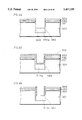
In recent semiconductor devices, miniaturized or fine isolation of elements have been desired, as higher integration of elements is in greater demand. The LOCOS (Local Oxidation of Silicon) method has been widely used as a method for element isolation. However, in element isolation by LOCOS method, bird's beaks are formed, which prevents provision of small width of isolation.
Consequently, a so called trench isolation technique using a narrow and deep trench has come to attract attention as a method of element isolating allowing fine element isolation. One example of the trench isolation technique is disclosed in Japanese Patent Laying Open-No. 63-170937.The element isolating structure disclosed in this Article will be described with reference to FIG. 70.
In the structure for isolation of a semiconductor device, a trench 31 is formed from a surface of p type semiconductor substrate 30 to a depth of about 1-2 μm. A side surface of trench 31 is covered with an oxide film 34, and a P+ type semiconductor layer 35 of a concentration of 1020 -1022 cm3 is formed with oxide film 34 interposed. In P type semiconductor substrate 30 contacting a bottom surface of trench 31, P+ type diffusion layer 36 of a concentration of 1020 -1022 cm3 for preventing formation of an inversion layer in the surface of p type semiconductor substrate 30 is formed and serves as a channel stopper. P+ type diffusion layer 36 also serves to prevent a punch through phenomenon. On an upper surface of P+ type semiconductor layer 35, an oxide film 38 is formed in a thickness of about 1000-2000Å. A gate oxide film 39 is formed on a surface of P type semiconductor substrate 30 except an area where oxide film 38 is formed.
A structure of a MOS transistor to which the structure for isolation is applied will be described hereinafter.
A gate electrode 40 is formed on gate oxide film 39 of the structure for isolation described above. Source/drain regions 41 of N+ type impurity region are formed to a predetermined depth on both sides of gate electrode 40.
Gate electrode 40 is covered with interlayer insulating film 42. A metallic interconnection 43 electrically connected to gate electrode 40 is formed to extend beneath interlayer insulating layer 42 above trench 31.
A manufacturing method of the structure for isolation will be described hereinbelow with reference to FIGS. 71 through 75.
Referring to FIG. 71, a thin thermal oxide film 32 having a thickness of about 300Å is formed on P type semiconductor substrate 30. A nitride film 33 is grown by a CVD method, and regions of nitride film 33, oxide film 32 and semiconductor substrate 30 which are to be regions for isolation are etched to a depth of about 1-2 μm to form trench 31.
Referring to FIG. 72, after a thermal oxide film 34 is formed relatively thick on a sidewall portion of trench 31, thermal oxide film 34 in the bottom portion of trench 31 is etched away by anisotropic etching to expose semiconductor substrate 30. Since a transistor forming region is covered with nitride film 33 which serves as a mask, etching of the region is prevented. Thereafter, a polycrystalline silicon 35 is grown to about 1-2 μm on the entire surface of the substrate including trench 31.
Referring to FIG. 73, impurities of a p type conductivity which is the same as that of the substrate are introduced into polycrystalline silicon 35 at a high concentration by an ion implantation or a gas phase doping, and diffused so deeply as to reach semiconductor substrate 30 contacting polycrystalline silicon 35 at the bottom surface portion of trench 31 in heat treatment. P+ type diffusion layer 36 is then formed as a channel stopper in semiconductor substrate 30 under the bottom portion of trench 31. Since the transistor forming region is covered with nitride film 33, impurities are not diffused into the region. Also, the side surface of trench 31 is covered with thermal oxide film 34, and therefore impurities are not diffused thereto. A photoresist film 37 is formed to flatten the surface of polycrystalline silicon 35.
Photoresist film 37 and polycrystalline silicon 35 having diffused impurities are etched back by anisotropic etching until the surface of nitride film 33 is exposed. As shown in FIG. 74, a structure in which polycrystalline silicon 35 fills trench 31 is thus finished. Thereafter, semiconductor substrate 30 is thermally oxidized and a relatively thin oxide film 38 is formed in a thickness of about 1000Å-2000Å on a surface of polycrystalline silicon 35 embedded in trench 31. Nitride film 33 and thermal oxide film 32 are removed, and a gate oxide film 39 is formed (FIG. 75). The structure for isolation is thus finished.
After the structure for isolation shown in FIG. 75 is formed, gate electrode 40 is patterned to a predetermined shape and source/drain regions 41 are formed. Interlayer insulating film 42 is grown, a contact hole is opened at a predetermined position and metallic interconnection 43 is provided. AMOS transistor as shown in FIG. 70 is then finished.
A manufacturing method of a CMOS transistor having the structure for isolation of a semiconductor device will be described hereinbelow with reference to FIGS. 76 through 87.
Referring to FIG. 76, after a right half surface of a p type semiconductor substrate 51 is covered with a resist film 52, phosphorus (P) is implanted to a predetermined depth in a left half region of p type semiconductor substrate 51 under conditions of 500 KeV-1.5 MeV and 1×10¹² -1×1015 cm-2. Heat treatment is carried out for 20 minutes to 10 hours at temperature of 800°-1200° C. to form an n type impurity diffusion region 53.
Referring to FIG. 77, after resist film 52 is removed, a surface of n+ impurity diffusion region 53 of p type semiconductor substrate 51 is covered with a resist film 54. Boron (B) is implanted into a right half region of p type semiconductor substrate 51 under conditions of 200 KeV-1 MeV and 1×10¹² -1×1015 cm-2. Heat treatment is carried out for 20 minutes-10 hours at temperature of 800°-1200° C. to form a p type impurity diffusion region 55.
Referring to FIG. 78, after resist film 54 is removed, a thin thermal oxide film 56 of a thickness of about 300Å is formed on surfaces of n type impurity diffusion region 53 and p type impurity diffusion region 55 and a nitride film 57 is grown on oxide film 56 using the CVD method. Thereafter, a resist film 58 is formed on nitride film 57 and is patterned. Using resist film 58 as a mask, regions of nitride film 57, oxide film 56, n type impurity diffusion region 53 and p type impurity diffusion region 55 which are to be an isolation region are etched to a depth of about 1-2 μm, so that trenches 59, 60 are formed as shown in FIG. 79.
Referring to FIG. 80, after resist film 58 is removed, thermal oxide films 61, 62 are formed relatively thick in trenches 59, 60. Thermal oxide films 61, 62 on bottom surfaces of trenches 59, 60 are removed by anisotropic etching to expose semiconductor substrate 51. At this time, n type impurity diffusion region 53 and p type impurity diffusion region 55 are not etched, since they are covered with nitride film 57 which serves as a mask. Thereafter, referring to FIG. 81, a polycrystalline silicon 70 is grown to about 1-2 μm on the entire surface of semiconductor substrate 51 including trenches 59, 60.
Referring to FIG. 82, a surface of polycrystalline silicon 70 above p type impurity diffusion region 55 is again covered with resist film 63, and phosphorus (P) is implanted into polycrystalline silicon 70 above n type impurity diffusion region 53 under conditions of 100 KeV and 1×10¹² -1×1016 cm-2.
After resist film 63 is removed, referring to FIG. 83, a resist film 64 is formed on n+ type impurity diffusion region 70a of a high concentration. Boron (B) is implanted into polycrystalline silicon 70 above p type impurity diffusion region 55 under conditions of 50 KeV and 1×10¹² -1×1016 cm-2 in the same manner as is described above.
After resist film 64 is removed, referring to FIG. 84, photoresist film 65 is provided on surfaces of p+ type impurity diffusion region 70a and n+ type impurity diffusion region 70b to flatten these surfaces. Referring to FIG. 85, photoresist film 65, n+ type impurity diffusion region 70a and p+ type impurity diffusion region 70b are etched back, and nitride film 57 is exposed. Heat treatment is carried out under conditions of temperature of 800° C.-1200° C. and a time of 20 minutes-10 hours. Impurities in n type impurity diffusion region 70a and p+ type impurity diffusion region 70b are diffused from bottom portions of trenches 59, 60, respectively to substrate 51. As a result, a structure is formed, in which n+ type impurity diffusion region 70a and p+ type impurity diffusion region 70b are embedded in trenches 59 and 60, respectively, and n diffusion layer 53a and p+ diffusion layer 55a serving as channel stoppers exist in the bottom portions of these trenches.
Referring to FIG. 86, a semiconductor substrate 51 is thermally oxidized, and relatively thin oxide films 66, 67 (about 1000-2000Å) are formed on the surfaces of n+ type impurity diffusion region 70a and p+ type impurity diffusion region 70b embedded in trenches 59, 60. Thereafter, nitride film 57 and thermal oxide film 56 are removed and a gate oxide film 68 is formed.
A structure for isolation used for a CMOS is thus finished.
Thereafter a gate oxide film 80 is deposited and a gate electrode 81 is formed. Gate electrode 81 is etched to have a predetermined shape using photolithography. Source/ drain regions 82, 83 are each formed in the substrate. An interlayer oxide film 84 is deposited on the entire surface of the substrate. Contact holes 85 reaching source/ drain regions 82, 83 are opened using photolithography. Aluminum 86 is deposited by sputtering and aluminum 86 is etched using photolithography. A CMOS transistor as shown in FIG. 87 is thus finished.
However, the structure of the semiconductor for element isolation described above has the following problem.
First, referring to FIG. 88, a first problem will be described. The p+ semiconductor layer 35 has high impurity concentration in the range of 1×10²⁰ to 1×1022 cm3. Therefore, when a gate electrode is formed on the oxide film 38 as shown in the figure, a capacitor C1 having a large parasitic capacitance is formed by the gate electrode 40, the oxide film 38 and the p+ semiconductor layer 35.
The existence of the capacitor C1 represented in an equivalent circuit is as shown in FIG. 89. As the capacitor C1 exists, electrons are charged/discharged to and from the capacitor C1 on the output side (OUT) of the circuit, which causes delay in signals. Therefore, as shown in the graph of FIG. 90, the speed of the device becomes slower.
When the impurity concentration of the semiconductor layer 35 is decreased to solve the above described problem, the semiconductor layer 35 comes to have a nature near an insulator. Therefore, as shown in FIG. 91, the electric field E from the gate electrode 4 inverts the sidewalls of the trench 31 directly, causing degradation of isolation.
Secondly, as shown in FIG. 92, in heat treatment necessary to form a channel stopper region in a bottom portion of a trench, since the impurity concentration is as high as 1020 -1022 cm3, impurities are widely diffused into a substrate to raise an impurity concentration in the vicinity of a surface of the substrate, so that a threshold voltage is increased. As shown in FIGS. 93(a), 93(b), when an isolation width is small, impurity diffusion regions from both isolation regions overlap each other and the concentration is liable to rise. This phenomenon appears more remarkably in a narrow channel. Since atomic radii of silicon and boron are different, defects are liable to be caused in the substrate, resulting in generation of leakage current.
Thirdly, when the above described structure of a semiconductor device is used for a CMOS structure, the number of manufacturing steps is extremely large and reliability must be secured in every step. Therefore, improvement of reliability of products, reduction of the cost and increase of a yield are hindered.
SUMMARY OF THE INVENTION
An object of the present invention is to provide a semiconductor device for element isolation having a structure for isolation in a form of a trench without a need of a channel stopper region.
Another object of the present invention is to provide a manufacturing method of a semiconductor device for element isolation in which impurities are implanted and diffused into a substrate such that a band of maximum impurity concentration is positioned at a predetermined depth in the substrate.
A still further object of the present invention is to provide a semiconductor device for element isolation superior in element isolation and having highly reliable element isolating structure and to provide a manufacturing method thereof.
In order to attain the above described objects, in the semiconductor device for element isolation according to one aspect of the present invention, the semiconductor substrate has a main surface. The semiconductor substrate has a band of maximum impurity concentration of impurities of a first conductivity type at a prescribed depth from and approximately parallel to the main surface. The semiconductor substrate has lower impurity concentration between the main surface and the band of the maximum impurity concentration. A trench for isolation has a sidewall extending from the main surface to the band of the maximum impurity concentration, which trench for isolation is filled with an isolating material.
In this semiconductor device for element isolation, a uniform p+ high concentration region is substantially formed in the bottom portion of the isolation region, so that an isolation threshold value is not affected. Also, as to isolation breakdown voltage and anti-punch through property, a depletion layer from source/drain regions do not join because of the existence of the uniform p+ high concentration region, and therefore a punch through phenomenon can be effectively suppressed.
A semiconductor device for element isolation, according to another aspect of the present invention, for achieving the above-stated objects includes a semiconductor substrate having a first conductivity type impurity region whose impurity concentration attains the maximum at a predetermined depth from a surface in the depth direction; a trench formed from the surface of the semiconductor substrate to a predetermined depth in the impurity region of the first conductivity type; an impurity diffusion region of the first conductivity type provided in the trench with a space from the sidewall, having only its bottom portion in contact with the above-mentioned impurity region of the first conductivity type in the semiconductor substrate and having almost the same impurity concentration as the aforementioned impurity region of the first conductivity type; an oxide film covering an upper surface of the impurity diffusion region and the surface of the semiconductor substrate as well as filling the space between the internal sidewall of the trench and the impurity diffusion region.
According to the semiconductor device for element isolation, at first oxide films are provided on the sidewall portions of the trench as the isolating material provided in the trench. A semiconductor layer is provided inside the oxide films provided on the sidewalls of the trench. Thus the difference in the coefficient of thermal expansion of the isolating material and of the semiconductor substrate can be released. This prevents generation of cracks into the isolating materials, and hence generation of leak current can be avoided. Further, since a high impurity region of p+ is substantially formed approximately uniform at the bottom portion of the isolating region, the isolation threshold value is not affected. In addition, depletion layer from the source/drain regions do no extend because of the high impurity region of p+ uniformly with respect to the isolation breakdown voltage, that is, punch through immunity, and accordingly generation of punch through can be effectively suppressed.
In order to attain the above described aspect, according to one aspect of the method of manufacturing a semiconductor device for element isolation of the present invention, a trench is formed from a the main surface to a prescribed depth of a semiconductor substrate. An isolating material is provided in the trench. Impurities are introduced to the semiconductor substrate such that a band of a maximum impurity concentration exists approximately parallel to the main surface and at a prescribed depth from the main surface. Lower impurity concentration exists between the band of the maximum impurity concentration and the main surface, and the depth of the trench extends to the band of the maximum impurity concentration.
A manufacturing method of a semiconductor device for element isolation, according to another aspect of the present invention, for achieving the above-stated objects includes the steps of forming a trench having a predetermined depth in a semiconductor substrate; forming an oxide film on an internal surface except a bottom surface of the trench; depositing a semiconductor layer in the trench; implanting and diffusing impurities of a first conductivity type into the semiconductor substrate and the semiconductor layer such that impurity concentration attains the maximum at a depth of the bottom of the trench in the depth direction.
According to the manufacturing method, the number of impurity implantation steps can be decreased, whereby the number of steps of forming resist films is also decreased. Thus, a manufacturing process of a semiconductor device can be shortened.
Further, according to a still further aspect, the semiconductor device for element isolation of the present invention includes, in order to attain the above described objects, a semiconductor substrate having a main surface, a trench formed to a prescribed depth from the main surface, a pair of sidewall insulating films provided on the sidewalls of the trench, a buried layer having a prescribed impurity concentration buried in the trench surrounded by the pair of sidewall insulating films, an upper insulating film formed to cover the opening portion of the trench at the main surface, and a pair of conductive layers having higher impurity concentration than the buried layer formed at the side portions of the buried layer and in contact with the lower surface of the upper insulating film and in contact with inner surface of each of the sidewall insulating films.
In order to attain the above described objects, according to a still further aspect, the method of manufacturing a semiconductor device for element isolation of the present invention includes the following steps.
First, a trench having a prescribed depth is formed at the semiconductor substrate. Then, sidewall insulating films are formed on the sidewalls of the trench.
Then, a conductive layer having a prescribed impurity concentration is formed in contact with the inner walls of the sidewall insulating films, from the main surface of the semiconductor substrate to a prescribed depth in the trench. Thereafter, a buried layer having impurity concentration lower than the conductive layer is formed in the trench surrounded by the conductive layer and by the sidewall insulating films.
Thereafter, an upper insulating film having a prescribed thickness covering the opening portion of the trench is formed at the surface of the buried layer.
In accordance with the semiconductor device for element isolation and manufacturing method thereof of the present invention, a pair of conductive layers in contact with inner surfaces of the sidewall insulating films and in contact with the lower surface of the upper insulating film, provided near the side portions of the buried layer and having higher impurity concentration than the buried layer are provided. Consequently, impurity concentration of the buried layer as a whole can be set lower, which suppresses increase of parasitic capacitance. Since the conductive layer for the electric field from the gate electrode is provided, formation of inverted layer at the sidewall portions of the trench can be suppressed with the electric field suppressed by the conductive layer.
The foregoing and other objects, features, aspects and advantages of the present invention will become more apparent from the following detailed description of the present invention when taken in conjunction with the accompanying drawings.
BRIEF DESCRIPTION OF THE DRAWINGS
FIG. 1 is a cross section showing a structure of a semiconductor device for element isolation in accordance with a first embodiment of the present invention.
FIG. 2 is a cross sectional view showing another structure of the semiconductor device for element isolation in accordance with the first embodiment of present invention.
FIG. 3 (a) is a schematic diagram showing the separation threshold value, and FIG. 3 (b) shows relation between voltage and current.
FIG. 4 (a) is a schematic diagram showing separation breakdown voltage, and FIG. 4 (b) shows relation between the voltage and the current.
FIG. 5 is a diagram for comparing the separation threshold value in (a) LOCOS structure, (b) conventional structure and (c) the present embodiment.
FIG. 6 is a diagram for comparing separation breakdown voltage in (a) LOCOS structure, (b) conventional structure and (c) in the present embodiment.
FIG. 7 is a graph for obtaining set mixing ratio for making the each rate of silicon equal to the etch rate of resist.
FIGS. 8 to 18 are cross sections showing the first to eleventh steps of manufacturing in accordance with the first embodiment of the present invention.
FIG. 19 shows concentration distribution in the substrate when boron is implanted to the substrate at a prescribed energy and a prescribed concentration.
FIGS. 20 through 34 are cross sections showing the first to fifteenth steps of manufacturing a CMOS transistor in accordance with the present invention.
FIG. 35 is cross section showing a structure of a semiconductor device in accordance with a second embodiment of the present invention.
FIG. 36 is a schematic diagram showing operation principal of the structure shown in FIG. 35.
FIG. 37 shows relation between time and voltage showing the effect provided by the structure of FIG. 35.
FIG. 38 is a schematic diagram showing another effect provided by the structure shown in FIG. 35.
FIG. 39 shows relation between the gate voltage and the drain current showing the effect provided by the structure of FIG. 35.
FIGS. 40 to 50 are cross sections showing the first to eleventh steps of manufacturing in accordance with the second embodiment of the present invention.
FIG. 51 is a cross section showing a structure of a semiconductor device in accordance with a third embodiment of the present invention.
FIGS. 52 to 59 are cross sections showing the first to eighth steps of manufacturing in accordance with the third embodiment of the present invention.
FIG. 60 is a cross section showing another structure of the semiconductor device in accordance with the third embodiment of the present invention.
FIG. 61 is a cross section showing a structure of a semiconductor device in accordance with a fourth embodiment of the present invention.
FIGS. 62 to 69 are cross sections showing the first to eighth steps of manufacturing in accordance with the first embodiment of the present invention.
FIG. 70 is a cross section of a conventional semiconductor device.
FIGS. 71 to 75 are cross sections showing the first to fifth steeps of manufacturing the conventional semiconductor device.
FIGS. 76 to 87 show the first to twelfth steps of manufacturing a conventional CMOS transistor.
FIG. 88 is a cross section of a conventional semiconductor device.
FIG. 89 is an equivalent circuit diagram showing problems of a conventional element isolating structure.
FIG. 90 shows relation between time and voltage in the conventional structure.
FIG. 91 is a first schematic diagram showing a problem of the element isolating structure of the prior art.
FIG. 92 is a schematic diagram showing impurity diffusion during thermal processing in the conventional semiconductor device structure.
FIG. 93(a) is a schematic diagram showing impurity diffusion when the channel is wide in the structure of a conventional semiconductor device and FIG. 93(b) is a schematic diagram showing increase of concentration because of overlapped impurities when the channel is narrow in the structure of the conventional semiconductor device.
DESCRIPTION OF THE PREFERRED EMBODIMENTS
A semiconductor device and a manufacturing method according to a first embodiment of the present invention will be described hereinbelow with reference to FIGS. 1 through 18.
Referring to FIG. 1, a structure of the semiconductor device includes a semiconductor substrate 1 including an impurity region 1a of a first conductivity type, for example, a p type whose impurity concentration attains the maximum at a predetermined depth from the surface, and a trench 6 formed from a surface of p type impurity region 1a of semiconductor substrate 1 to a predetermined depth in p type impurity region 1a. A p type impurity diffusion region 8 is provided with a space from an internal sidewall, having only its bottom surface in contact with semiconductor substrate 1 and having almost the same concentration as impurity region 1a. An oxide film 11 is formed to fill the space between the internal sidewall of trench 6 and p type impurity diffusion region 8 and to cover an upper surface of impurity diffusion region 8 and the surface of semiconductor substrate 1.
Referring to FIG. 2, another structure will be described. In this structure, the inside of the trench 6 is entirely filled by an oxide film. However, in this structure, cracks are generated in the oxide film during the step of thermal processing, since the difference of the coefficient of thermal expansion between the semiconductor substrate 1 and the oxide film 11 is large. If a crack is generated in the oxide film, a leak current is generated in the semiconductor substrate, degrading the capability of element isolation. Therefore, a structure relaxing the difference of the coefficient of thermal expansion by the provision of the semiconductor layer in the trench such as shown in FIG. 1 is preferred. The structure shown in FIG. 1 is described in the following.
In a transistor forming region, a gate electrode 7 is formed on an upper surface of oxide film 11 and source/ drain regions 9, 10 of n+ type impurity regions are formed to a predetermined depth in impurity region 1a on both sides of gate electrode 7.
An isolation capability will be described hereinbelow. As to the isolation capability, both "an isolation threshold value" and "an isolation breakdown voltage" should be considered.
Referring to FIGS. 3 (a), and 3 (b), "an isolation threshold value" means a value of a gate voltage Vg at which left and right source/ drain regions 100, 101 are rendered conductive.
Referring to FIGS. 4 (a), "an isolation breakdown voltage" is a voltage applied to one of source/ drain regions 100, 101 when source/ drain regions 100, 101 are rendered conductive or a junction breakdown occurs. FIG. 4 (b) shows in the relationship between voltage Vd and current Id.
Isolation threshold values and isolation breakdown voltages of an LOCOS structure, a conventional structure and the structure of the present embodiment are compared for isolation capability.
When respective isolation threshold values are compared, referring to FIGS. 5(a), 5(b) and 5(c), in the LOCOS structure, a path L between elements 100, 101 is short, and also there is possibility for inversion in regions marked with X in path L, and therefore, it can be seen that it is easily rendered conductive.
In the conventional structure, a path between elements 100, 101 is long and inversion in regions marked with X in the sidewall portion of the trench does not occur and therefore it is not easily rendered conductive.
In the structure of the present embodiment, a path between elements 100, 101 is long, as in the conventional structure, inversion in regions marked with X in the sidewall portion of the trench does not occur and therefore it is not easily rendered conductive. Also, since p+ layer 103 of a high concentration is provided in the bottom portion of the trench, even if an inversion layer is formed, it is impossible to be rendered conductive and therefore isolation capability can be fully enhanced.
When isolation breakdown voltages are compared, referring to FIGS. 6(a), 6(b) and 6(c), since in the LOCOS structure, path L between element 100, 101 is short as described above, a punch through phenomenon is likely to occur.
In the conventional structure, since there is only one high concentration layer 102, a depletion layer is rendered conductive at a deep portion of the substrate, resulting in possibility of a punch through phenomenon.
However, in the structure of the present embodiment, by selecting impurity implantation energy to attain the maximum impurity concentration in the bottom portion of the trench, p+ layer 103 can be substantially formed in the bottom portion of the substrate. As a result, since depletion layers from the source/drain regions are not joined because of the existence of p+ layer 110, a punch through phenomenon can be effectively suppressed.
By using the above structure in an NMOS transistor, isolation can be achieved without providing a channel stopper region in a bottom portion of an isolation region.
In a manufacturing method of a semiconductor device having the above structure, referring to FIG. 8, a first oxide film 2 of SiO2 is formed in a thickness of about 300Å on a surface of a semiconductor substrate 1 using a thermal oxidation method. A first semiconductor layer 3 of polysilicon is formed in a thickness of about 500-2000Å on a surface of first oxide film 2 using the CVD method, and thereafter, a second oxide film 4 of SiO2 is formed in a thickness of about 300Å on a surface of first semiconductor layer 3 using a thermal oxidation method.
Referring to FIG. 9, a resist film 5 having a predetermined pattern is formed on a surface of second oxide film 4. Referring to FIG. 10, a trench 6 having a depth of about 0.3-1.0 μm is formed by anisotropic etching, using resist film 5 as a mask.
After trench 6 is formed, referring to FIG. 11, resist film 5 is removed and an oxide film is formed in an internal surface of trench 6 by a thermal oxidation method. At this time, first semiconductor layer 3 is further oxidized and second oxide film 4 is thickened. In a side surface portion of trench 6, second oxide film 4 and first oxide film 2 are united. The oxide film thus formed is hereinafter referred to as an oxide film 11 hereinafter.
Referring to FIG. 12, oxide film 11 in a bottom surface portion of trench 6 is etched away by anisotropic etching, so that semiconductor substrate 1 is exposed. Referring to FIG. 13, a second semiconductor layer 8 is epitaxially grown at a growth rate of 0.2-1.4 μm/min and at growth temperatures in a range of about 700° C. to 1200° C., using a gas such as SiCl4, SiHCl3, SiH2 Cl2, SiH4 in trench 6 and on a surface of oxide film 11.
Referring to FIGS. 14 and 15, to flatten a surface of semiconductor layer 8, a resist film 91 is formed flat on the surface of semiconductor layer 8 and etched back to a predetermined depth. In this etching, as shown in FIG. 7, CCl4 and O2 are mixed such that an etch rate for silicon and an etch rate for resist are equal.
Referring to FIG. 16, semiconductor layer 8 is thermally oxidized more deeply than the surface of semiconductor substrate 1, and oxide film 12 is formed.
Oxide film 11 and oxide film 12 are etched until a surface of semiconductor layer 3 is exposed. Referring to FIG. 17, only the exposed semiconductor layer 3 is etched away.
Referring to FIG. 18, impurities of one conductivity type, for example, boron (B) are simultaneously implanted and activated in semiconductor substrate 1 and second semiconductor layer 8 at a constant energy value in a range of 200 KeV-1 MeV and at a constant implantation amount in a range of 1×10¹² -1×1015 cm-2. When, for example, boron is implanted into the substrate under conditions of an implantation amount of 2×1013 cm-2 and energies of 1 MeV, 2 MeV, and 3 MeV, impurity concentration attains the maximum at depths of about 1.7 (μm), 2.8 (μm) and 4.0 (μm), respectively, as shown in FIG. 19. As a result, it is possible to maximize impurity concentration in a bottom portion of the substrate. Semiconductor layer 8 forms an impurity diffusion region 8a. An isolation region of the semiconductor device in this embodiment is then finished.
The number of implantation steps of impurity regions is decreased by employing the isolation structure without a channel stopper as described above. Therefore, the number of steps of forming resist films can be decreased and thus the manufacturing process can be shortened.
A manufacturing method of a CMOS transistor having the isolation regions of a semiconductor device will be described with reference to FIGS. 20 through 34. Referring to FIG. 20, a first oxide film 14 of SiO2 is formed at a thickness of about 30Å on a surface of a semiconductor substrate 13 using a thermal oxidation method. A first semiconductor layer 15 of polysilicon is formed in a thickness of about 500-2000Å on a surface of first oxide film 14 using a CVD method. Thereafter, a second oxide film 16 of SiO2 is formed in a thickness of about 300Å on a surface of first semiconductor layer 15.
Referring to FIG. 21, a resist film 17 having a pattern for formation of an isolation trench is formed on a surface of second oxide film 16. Referring to FIG. 22, using resist film 17 as a mask, trenches 18, 19 having a depth of about 0.3-1.0 μm are formed using anisotropic etching.
Referring to FIGS. 23 and 24, after resist film 17 is removed, oxide films are formed on internal surfaces of trenches 18, 19. At this time, first semiconductor layer 15 is further oxidized and a second oxide film 16 is thickened. In side surface portions of trenches 18, 19, second oxide film 16 and first oxide film 14 are united. An oxide film thus formed is hereinafter referred to as an oxide film 20.
Referring to FIG. 25, oxide film 20 in a bottom surface portions of trenches 18, 19 is etched by anisotropic etching and semiconductor substrate 13 is exposed. Referring to FIG. 26, a second semiconductor layer 21 is formed in a thickness of about 0.1 μm by epitaxial growth, in trenches 18, 19 and on a surface of oxide film 20 using a gas such as SiCl4, SiHCl3, SiH2 Cl2 and SiH4 at a growth rate of about 0.2-1.5 μm/min and grown temperatures in a range of 700° C. to 1200° C.
To flatten the surface of semiconductor layer 21, referring to FIGS. 27 and 28, a resist film 22 is formed flat on a surface of semiconductor layer 21 and etched back to a predetermined depth. In this etching, CCl4 for etching semiconductor layer 21 is mixed with O2 for etching resist film 22 such that both etching rates are equal. Referring to FIG. 29, impurities are thermally diffused more deeply than a surface of semiconductor substrate 1 in semiconductor layer 21, and an oxide film 23 is formed.
Oxide film 20 and oxide film 23 are etched until a surface of semiconductor layer 15 is exposed. Referring to FIG. 30, only the exposed semiconductor layer 15 is etched away.
Referring to FIG. 31, a resist film 25 is formed on a right half surface of oxide film 20. Using resist film 25 as a mask, phosphorus (P) is implanted at a constant energy values in a range of 500 KeV-1.5 MeV and at a constant implantation amount in a range of 1×10¹² -1×1015 cm-2. Thermal diffusion is carried out at a temperature of 800°-1200° C. for 20 minutes-10 hours to form an n type diffusion impurity region 26 whose impurity concentration attains the maximum in a bottom portion of the substrate. At this time, phosphorus (P) is simultaneously implanted and diffused in second semiconductor layer 21 formed in trench 18, and an n type impurity diffusion layer 21a is formed.
Referring to FIG. 32, a resist film 27 is formed on a left half surface of oxide film 20 in the same manner as is described above. Using resist film 27 as a mask, boron (B) is implanted and diffused to a predetermined depth in a right half of semiconductor substrate 13, and a p type impurity diffusion region 28 is formed. Simultaneously, boron (B) is also implanted into a second semiconductor device 21 formed in trench 19 under conditions of respective constant values in a range of 200 KeV-1 MeV and 1×10¹² -1×1015 cm-2. Thermal diffusion is carried out at a temperature of 800°-1200° C. for 20 minutes-10 hours and p type impurity diffusion layer 21b is then formed whose impurity concentration attains the maximum in a bottom portion of the substrate.
Resist film 27 is removed, so that an isolation region used for a CMOS transistor as shown in FIG. 33 is finished.
Thereafter, gate oxide film 11 is deposited and gate electrode 7 is formed. Gate electrode 7 is etched to a predetermined shape using photolithography. Source/ drain regions 9, 10 are formed in respective wells. An interlayer oxide film 24 is deposited on the whole surface of the substrate. Contact holes 24a reaching source/ drain regions 9, 10 are opened using photolithography. Aluminum 29 is deposited by sputtering and etched by photolithography. An CMOS transistor as shown in FIG. 34 is then finished.
Although, in the above embodiment, an epitaxial layer is formed to form the p type impurity diffusion region in the second semiconductor layer formed in the trench, metallic material of tungsten (W) may be deposited instead. In this case, a mixed gas of Wf6 and SiH4, or Wf6 and H2 is used at temperatures in range of about 400°-1000° C. in the CVD method. When the second semiconductor layer is formed of tungsten (W), impurities are not diffused into the layer but only into the semiconductor substrate.
For the CMOS transistor having the isolation structure without a channel stopper, as described above, the number of implantation steps of impurities is decreased, the number of steps of forming resist films is decreased to a half, so that the number of manufacturing steps can be decreased.
In the embodiments according to the present invention, since a channel stopper region needed in a bottom portion of a trench in a conventional case is not provided, it is possible to shorten the manufacturing process. Particularly, when a semiconductor device of the structure according to the present embodiment is used in a CMOS transistor, it is possible to greatly shorten the manufacturing process, to increase reliability of products and to reduce the cost.
A second embodiment of the present invention will be described.
The element isolating structure of the embodiment will be described with reference to FIG. 35.
A trench 506 is formed to have the depth of about 1 to 2μ from the main surface of a p type semiconductor substrate 501. A pair of sidewall insulating films 562 and 562 of oxide films are formed on the sidewalls of the trench 506. In the trench 506 surrounded by the pair of sidewall insulating films 562 a buried layer 510 having the impurity concentration in the range of 1×10¹⁴ to 1×1017 cm-3 is provided. In this embodiment, the buried layer 510 has a two layered structure including a lower buried layer 510a and an upper buried layer 510b. The upper opening portion of the trench 506 is covered by an upper insulating film 503 of an oxide film. In the region of the buried layer 510, a pair of conductive layers 520 and 520 having the impurity concentration of about 1×10¹⁸ to 1×1021 cm-3 are provided in contact with the lower surface of the upper insulating film 503 and inner surfaces of the sidewall insulating films 562 and near the side portions of the buried layer are provided.
A case in which a gate electrode 530 is provided on the above described element isolating structure will be described with reference to FIG. 36.
In the structure of the above embodiment, since the buried layer 510 having low impurity concentration is positioned at the lower surface of the upper insulating film 503, the depletion layer 540 is formed entirely over the upper region of the buried layer 510. Therefore, the parasitic capacitance of the capacitor formed by the gate electrode 530, the upper electrode 503 and the buried layer 510 can be reduced. Consequently, speed of operation of the device isolated by this element isolating structure can be improved as shown in FIG. 37. In addition, with respect to the electric field E from the gate electrode 530, the electric field E can be shielded by the conductive layers 520, as shown in FIG. 38. Therefore, the conductive layer 520 prevents inversion of the semiconductor substrate 501 at the edge portion of the trench 506. Thus the parasitic component of the transistor is cut, and a phenomenon in which the channel is not completely turned OFF can be prevented as shown in FIG. 39, allowing reduction of power.
The method of manufacturing the above described element isolation will be described with reference to FIGS. 40 to 50. FIGS. 40 to 50 are cross sections in accordance with the cross sectional structure shown in FIG. 35.
Referring to FIG. 40, a first oxide film 551 of SiO2 is formed to have the thickness of about 300Å by thermal oxidation on the surface of the semiconductor substrate 501. A silicon nitride film 552 is formed by the CVD method to the thickness of about 2000Å on the surface of the first oxide film 551. Thereafter, a second oxide film 553 of SiO2 is formed to the thickness of about 2000Å by thermal oxidation on the silicon nitride film 512.
Thereafter, a resist film having a prescribed pattern (not shown) is formed on the second oxide film 513. Thereafter, by using the resist film as a mask, a trench 506 having the depth of about 0.3 to 1.0μ is formed by an isotropic etching.
Then, referring to FIG. 41, the resist film is removed, and an oxide film 562 having the thickness of about 300Å is formed on the inner surface of the trench 506 by thermal oxidation. Thereafter, referring to FIG. 42, the oxide film 562 formed at the bottom portion of the trench 506 only is removed by anisotropic etching.
Thereafter, referring to FIG. 43, a polysilicon having the low impurity concentration of about 1×1014 cm-3 is deposited by the CVD method on the entire surface of the substrate. Then, referring to FIG. 44, the polysilicon layer 55 is etched back to lead the polysilicon layer 554 at a prescribed region at the bottom of the trench 506 only, to form the lower buried layer 510a.
Then, referring to FIG. 45, a high concentration polysilicon 512 having the impurity concentration of 1× 1018 cm-3 or higher is formed on the entire surface of the substrate by the CVD method, to the thickness of about 200 to 3000Å. The high concentration polysilicon layer 512 has the same conductivity as the substrate, and in this embodiment, it has p type conductivity.
Then, referring to FIG. 46, the polysilicon layer 512 formed at the upper portion of the lower buried layer 510a is removed by anisotropic etching.
Then, referring to FIG. 48, the polysilicon layer 522 is etched back. Thus an upper buried layer 510b is formed in the trench 506.
Then, referring to FIG. 49, the second oxide film 553 shown in FIG. 48 is removed by etching. Thereafter, as shown in FIG. 50, an upper insulating film 503 is formed by using the silicon nitride film 553 as a mask by a method similar to the conventional LOCOS method, by thermal oxidation. Thereafter, the silicon nitride film 553 is removed by wet etching using phosphoric acid, and the element isolation structure shown in FIG. 35 is thus completed.
As described above, by this embodiment, a pair of conductive layers having higher impurity concentration than the buried layer are provided near the side portions of the buried layer and in contact with the lower surface of the upper insulating film and in contact with the inner surfaces of the sidewall insulating films. Thus the impurity concentration of the buried layer as a whole can be set lower, suppressing parasitic resistance. In addition, as to the electric field from the gate electrode, the electric field is suppressed by the conductive layers and thus formation of inverted layer at the sidewall portions of the trench can be prevented.
A third embodiment of the present invention will be described.
Referring to FIG. 51, the element isolating structure of this embodiment will be described.
The element isolating structure of the third embodiment differs from the structure of the second embodiment described above in the following points.
First, the conductive layers 520 and 520 are formed to the bottom of the trench 506. At the bottom of the trench 506, a bottom conductive layer 522 is formed. The buried layer 510 is entirely formed of polysilicon layer of low impurity concentration.
As to the impurity concentration of the buried layer 510 as a whole, it should preferably be low in view of parasitic capacitance. Therefore, the ratio of the buried layer 510 occupied by the conductive layer 522 should be as small as possible. However, in the structure of the second embodiment, during the steps of manufacturing, there may possibly be a natural oxide film 555 formed between the semiconductor substrate 501 and the lower buried layer 510b and between the lower buried layer 510b and the upper buried layer 510a. Because of the natural oxide film 555, conductivity between the buried layer 510 and the semiconductor substrate 510 cannot be ensured, causing potential difference between the buried layer 510 and the semiconductor substrate 501.
The third embodiment is made to solve the above described the problem of the second embodiment.
As shown in FIG. 51, by providing the bottom portion conductive layer 522 at the bottom of the trench 506, conductivity between the semiconductor substrate 501 and the buried layer 510 can be ensured, and therefore the potentials of the semiconductor layer 501 and of the buried layer 510 can be surely kept at the same potential.
Manufacturing steps of the element isolating structure described above will be described with reference to FIGS. 52 to 59. FIGS. 52 to 59 are cross sections in accordance with the cross sectional structure shown in FIG. 51.
Referring to FIG. 52, a first oxide film 551 of SiO2 is formed to the thickness of 300Å by thermal oxidation on the surface of the semiconductor substrate 501. A silicon nitride film 552 having the thickness of about 2000Å is formed on the surface of the first oxide film 551. Further, a second oxide film 553 is formed to the thickness of about 2000Å by thermal oxidation on the silicon nitride film 552.
Then, a resist film having a prescribed pattern (not shown) is formed on the second oxide film 553. Thereafter, by using the resist film as a mask, a trench 506 having the depth of about 0.3 to 1.5μ is formed by anisotropic etching.
Then, referring to FIG. 53, after the resist film is formed, sidewall oxide films 562 are formed on the sidewalls of the trench 506 by thermal oxidation. Thereafter, the sidewall oxide film 562 formed at the bottom of the trench 506 only is removed by anisotropic etching.
Then, referring to FIG. 55, a polysilicon 512 of high concentration having the impurity concentration of 1×1018 cm-3 or higher is deposited to the thickness of about 200 to 3000Å by the CVD method on the entire surface of the substrate. The same conductivity as the substrate is selected as the conductivity of the impurities, and in this embodiment, it has p type conductivity.
Then, as shown in FIG. 56, a polysilicon not doped with impurities is deposited on the entire surface of the substrate. At this time, the sum of the thickness of the high concentration polysilicon layer 512 and the thickness of the polysilicon layer 522 should be about 1.5 times that of the width of the trench 506.
Then, referring to FIG. 57, the polysilicon layer 522 is removed by etchback to leave the polysilicon layer only in the trench 506 and to form the buried layer 510. Then, referring to FIG. 58, the second oxide film 553 is removed by wet etching.
Then, referring to FIG. 59, the upper insulating film 503 is formed by using the silicon nitride film 553 as a mask by a similar method as the common LOCOS method, by thermal oxidation. Thereafter, by removing the silicon nitride film 553 by wet etching, the element isolating structure in accordance with the third embodiment shown in FIG. 51 is completed.
In the step of FIG. 59, by controlling the process time for forming the upper insulating film 3, the thickness of the upper insulating film 503 can be made thick as shown in FIG. 60, and therefore it is also possible to locate the lower surface of the upper insulating film 3 below the main surface of the semiconductor substrate 1. By the structure shown in FIG. 60, even if the gate electrode is arranged on the upper insulating film, the parasitic capacitance can be further reduced since the gate electrode is sufficiently distant from the buried layer 510. In addition, since the upper insulating film is thick, even if the upper insulating film is etched to some extent in the succeeding process steps, possibility of short circuit between the buried layer 510 and the upper interconnections, caused by possible exposure of the buried layer 510, can be prevented.
The same effects as the second embodiments can be obtained by the third embodiment.
A fourth embodiment of the present invention will be described.
The element isolating structure in this embodiment will be described with reference to FIG. 61. The element isolating structure of the fourth embodiment differs from the third embodiment above in the following points.
Different from the third embodiment, a high concentration impurity layer 566 is formed on the bottom surface of and on the side surfaces on the side of the semiconductor substrate 501 of the trench 506. This layer is formed to prevent a so called inverse narrow effect generated in a semiconductor element such as a MOS transistor, formed in the element isolating region when space between adjacent element isolating regions become narrow as the semiconductor device is miniaturized.
The inverse narrow effect refers to a phenomenon such as shown in FIG. 38, in which electric field E from the gate electrode 530 on the upper insulating film 503 goes to the side of the active region to invert the side surface with low impurity concentration at a low threshold voltage. The inverted layer having low threshold exists in any transistor having an arbitrary channel width. Especially in a transistor having small channel width, the ratio occupied by the side surface becomes large, lowering threshold value of the transistor. This phenomenon, in which threshold becomes lower as the channel width becomes narrower is called the inverse narrow effect.
The manufacturing steps of the element isolating structure of the fourth embodiment will be described with reference to FIGS. 62 to 69. FIGS. 62 to 69 are cross sections in accordance with the cross sectional structure of FIG. 61.
First, referring to FIG. 62, a first oxide film 511 of SiO2 or the like is formed to the thickness of about 300Å by thermal oxidation on the surface of the semiconductor substrate 501. Thereafter, a silicon nitride film is formed to the thickness of 2000Å by the CVD method on the first oxide film 2. Thereafter, a second oxide film 553 of SiO2 or the like is again formed to about 2000Å on the silicon nitride film 552. Thereafter, a resist film having a prescribed pattern (not shown) is formed on the surface of the second oxide film 553. Then, a trench 506 having the depth of about 0.3 to 1.0μ is formed by anisotropic etching, using the resist film as a mask.
Then, an oxide film 562 is formed by thermal oxidation entirely over the surface of the substrate. Thereafter, referring to FIG. 54, the oxide film 562 formed at the bottom of the trench 506 only is removed by an isotropic etching.
Thereafter, as shown in FIG. 64, impurities are introduced to the sidewalls and at the bottom surface of the trench 506 with the dosage of the 1×1013 cm-2 and at the energy of 50 KeV by oblique rotary ion implantation, to form a high concentration impurity layer 566 having the impurity concentration of 1×1018 cm-3.
And, referring to FIG. 65, a high concentration polysilicon layer 521 having the impurity concentration of 1×1018 cm-3 or higher is formed to the thickness of 200 to 3000Å by the CVD method on the entire surface of the substrate.
Then, referring to FIG. 66, a polysilicon layer 522 not doped with impurities is deposited on the entire surface of the substrate. Then, referring to FIG. 67, the polysilicon layer 522 is etched back to form a buried layer 510 in the trench 506.
Then, the second oxide film 552 is removed by wet etching.
Then, referring to FIG. 69, an upper insulating film 503 is formed by using the silicon nitride film 553 as a mask by a similar method as the common LOCOS method, by thermal oxidation. Thereafter, the silicon nitride film 553 is removed by wet etching using phosphoric acid, and thus the element isolating structure shown in FIG. 61 is completed.
In the fourth embodiment described above, the same effect as the second embodiment can be provided. In addition, the inverse narrow effect can be suppressed.
Although the present invention has been described and illustrated in detail, it is clearly understood that the same is by way of illustration and example only and is not to be taken by way of limitation, the spirit and scope of the present invention being limited only by the terms of the appended claims.

Claims (19)

What is claimed is:
1. A semiconductor device for element isolation, comprising:
a semiconductor substrate having a main surface, said substrate comprising an impurity region of a first conductivity type having a band of maximum impurity concentration substantially parallel to said surface and at a predetermined depth therefrom, said substrate having a smaller impurity concentration of said first conductivity type between said band and said main surface; and
an isolation trench having sidewalls and a bottom extending from the main surface to said band, said trench filled with an isolation material and wherein said band extends laterally from a portion of said trench sidewalls and said bottom in contact with said band and wherein said substrate, said impurity region of said substrate, said band of maximum impurity concentration and said small impurity concentration are of the same conductivity type.
2. The semiconductor device for element isolation according to claim 1, wherein
said isolation material is silicon oxide.
3. The semiconductor device for element isolation according to claim 1, wherein said isolation material has a thermal expansion coefficient similar to the thermal expansion coefficient of the substrate.
4. The semiconductor device for element isolation according to claim 1, wherein
said isolation material comprises an oxide film.
5. The semiconductor device for element isolation according to claim 1, wherein
said maximum impurity concentration is of a value of at least 1×10¹⁶ ions/cm3.
6. The semiconductor device for element isolation according to claim 3, wherein
said substrate is a silicon substrate and said isolation material comprises polysilicon in contact with said substrate at said band.
7. The semiconductor device for element isolation according to claim 3, wherein
said substrate is a silicon substrate and said isolation material comprises single crystal silicon in contact with said substrate at said band.
8. The semiconductor device for element isolation according to claim 6, wherein
said trench further comprises an oxide film extending between each of said sidewalls and said polysilicon and covering an upper surface of said polysilicon.
9. The semiconductor device for element isolation according to claim 6, wherein
said polysilicon contains impurities of said first conductivity type.
10. The semiconductor device for element isolation according to claim 7, wherein
said trench further comprises an oxide film extending between each of said sidewalls and said single crystal silicon and covering an upper surface of said single crystal silicon.
11. The semiconductor device for element isolation according to claim 7, wherein
said single crystal silicon contains impurities of said first conductivity type.
12. A semiconductor device for element isolation, comprising:
a semiconductor substrate having an impurity region of a first conductivity type having impurity concentration reaching a maximum value at a predetermined depth from a surface in the depth direction;
a trench formed to a predetermined depth from the surface of said semiconductor substrate in said impurity region of a first conductivity type wherein said impurity concentration of maximum value extends laterally in a band from a bottom of said trench;
an impurity diffusion region of said first conductivity type provided with a space from an internal sidewall of the trench in said trench, having only its bottom portion connected to said impurity region of the first conductivity type of said semiconductor substrate and having almost the same impurity concentration as said impurity region of the first conductivity type; and
an oxide film filling the space between the internal sidewall of said trench and said impurity diffusion region, and covering an upper surface of said impurity diffusion region and a surface of said semiconductor substrate; wherein said substrate, said impurity region of said semiconductor substrate, said impurity concentration of maximum valve and said impurity diffusion region are of the same conductivity type.
13. The semiconductor device for element isolation according to claim 12, wherein the maximum value of an impurity concentration in said impurity region of the first conductivity type is 1×10¹⁶ ions/cm3.
14. A semiconductor device, comprising: a semiconductor substrate of a first conductivity type having a main surface;
a trench formed at a prescribed depth from said main surface;
a pair of sidewall insulating films extending along sidewalls of said trench to said prescribed depth;
a buried layer having a prescribed impurity concentration of said first conductivity type, buried in said trench surrounded by said pair of sidewall insulating films;
an upper insulating film formed to substantially cover the trench at said main surface; and
a pair of conductive layers of said first conductivity type and having higher impurity concentration than said buried layer which are in contact with a lower surface of said upper insulating film and with inner surfaces of sidewall insulating films in the region of said buried layer and provided near a side portion of said buried layer, said pair of conductive layers extending in said trench at a depth less than said prescribed depth and being the only region of higher impurity concentration of the first conductivity type in said trench.
15. The semiconductor device for element isolation according to claim 14, wherein
said pair of conductive layers include a bottom conductive layer having a prescribed impurity concentration for coupling the respective conductive layers.
16. The semiconductor device for element isolation according to claim 15, wherein
said pair of conductive layers and said bottom conductive layer have the same impurity concentration.
17. The semiconductor device for element isolation according to claim 15, comprising:
an external conductive layer having a prescribed impurity concentration formed to be in contact with an outer side of said pair of internal insulating films from the surface of said semiconductor substrate, and to cover the pair of internal insulating films and said bottom conductive layer.
18. The semiconductor device for element isolation according to claim 17, wherein
said pair of conductive layers, said bottom conductive layer and said external conductive layer have the same impurity concentration.
19. The semiconductor device for element isolation according to claim 14, wherein
a part of the lower surface of said upper insulating film is positioned lower than the position of the main surface of said semiconductor substrate.
US08/252,629 1992-01-17 1994-06-02 Semiconductor device for element isolation and manufacturing method thereof Expired - Lifetime US5457339A (en)

Priority Applications (1)

Application Number Priority Date Filing Date Title
US08/252,629 US5457339A (en) 1992-01-17 1994-06-02 Semiconductor device for element isolation and manufacturing method thereof

Applications Claiming Priority (6)

Application Number Priority Date Filing Date Title
JP4-006567 1992-01-17
JP656792 1992-01-17
JP04326457A JP3092834B2 (en) 1992-01-17 1992-12-07 Semiconductor device for element isolation and method of manufacturing the same
JP4-326457 1992-12-07
US283693A 1993-01-14 1993-01-14
US08/252,629 US5457339A (en) 1992-01-17 1994-06-02 Semiconductor device for element isolation and manufacturing method thereof

Related Parent Applications (1)

Application Number Title Priority Date Filing Date
US283693A Continuation 1992-01-17 1993-01-14

Publications (1)

Publication Number Publication Date
US5457339A true US5457339A (en) 1995-10-10

Family

ID=26340748

Family Applications (1)

Application Number Title Priority Date Filing Date
US08/252,629 Expired - Lifetime US5457339A (en) 1992-01-17 1994-06-02 Semiconductor device for element isolation and manufacturing method thereof

Country Status (2)

Country Link
US (1) US5457339A (en)
DE (1) DE4300986C2 (en)

Cited By (21)

* Cited by examiner, † Cited by third party
Publication number Priority date Publication date Assignee Title
US5541440A (en) * 1993-07-28 1996-07-30 Mitsubishi Denki Kabushiki Kaisha Isolation structure for semiconductor device
US5604159A (en) * 1994-01-31 1997-02-18 Motorola, Inc. Method of making a contact structure
US5646063A (en) * 1996-03-28 1997-07-08 Advanced Micro Devices, Inc. Hybrid of local oxidation of silicon isolation and trench isolation for a semiconductor device
US5742090A (en) * 1996-04-04 1998-04-21 Advanced Micro Devices, Inc. Narrow width trenches for field isolation in integrated circuits
US5763932A (en) * 1996-11-12 1998-06-09 Micron Technology, Inc. Isolation regions and methods of forming isolation regions
US5777370A (en) * 1996-06-12 1998-07-07 Advanced Micro Devices, Inc. Trench isolation of field effect transistors
US5780353A (en) * 1996-03-28 1998-07-14 Advanced Micro Devices, Inc. Method of doping trench sidewalls before trench etching
US5859466A (en) * 1995-06-07 1999-01-12 Nippon Steel Semiconductor Corporation Semiconductor device having a field-shield device isolation structure and method for making thereof
US5861104A (en) * 1996-03-28 1999-01-19 Advanced Micro Devices Trench isolation with rounded top and bottom corners and edges
US5874317A (en) * 1996-06-12 1999-02-23 Advanced Micro Devices, Inc. Trench isolation for integrated circuits
US5904543A (en) * 1996-03-28 1999-05-18 Advanced Micro Devices, Inc Method for formation of offset trench isolation by the use of disposable spacer and trench oxidation
US5960297A (en) * 1997-07-02 1999-09-28 Kabushiki Kaisha Toshiba Shallow trench isolation structure and method of forming the same
US6057243A (en) * 1998-02-23 2000-05-02 Sony Corporation Method for producing semiconductor device
US6097072A (en) * 1996-03-28 2000-08-01 Advanced Micro Devices Trench isolation with suppressed parasitic edge transistors
US6097069A (en) * 1998-06-22 2000-08-01 International Business Machines Corporation Method and structure for increasing the threshold voltage of a corner device
US6184105B1 (en) 1997-05-22 2001-02-06 Advanced Micro Devices Method for post transistor isolation
US6214696B1 (en) * 1998-04-22 2001-04-10 Texas Instruments - Acer Incorporated Method of fabricating deep-shallow trench isolation
US20010014511A1 (en) * 1997-01-27 2001-08-16 Pai Hung Pan Technique for forming shallow trench isolation structure without corner exposure and resulting structure
US6353253B2 (en) * 1996-05-02 2002-03-05 Advanced Micro Devices, Inc. Semiconductor isolation region bounded by a trench and covered with an oxide to improve planarization
US20030209767A1 (en) * 2002-05-10 2003-11-13 Fujitsu Limited Nonvolatile semiconductor memory device and method for fabricating the same
US6674134B2 (en) * 1998-10-15 2004-01-06 International Business Machines Corporation Structure and method for dual gate oxidation for CMOS technology

Citations (13)

* Cited by examiner, † Cited by third party
Publication number Priority date Publication date Assignee Title
US4309716A (en) * 1979-10-22 1982-01-05 International Business Machines Corporation Bipolar dynamic memory cell
US4473598A (en) * 1982-06-30 1984-09-25 International Business Machines Corporation Method of filling trenches with silicon and structures
US4520552A (en) * 1980-04-14 1985-06-04 Thomson-Csf Semiconductor device with deep grip accessible via the surface and process for manufacturing same
US4556585A (en) * 1985-01-28 1985-12-03 International Business Machines Corporation Vertically isolated complementary transistors
US4729964A (en) * 1985-04-15 1988-03-08 Hitachi, Ltd. Method of forming twin doped regions of the same depth by high energy implant
JPS63151070A (en) * 1986-12-16 1988-06-23 Matsushita Electric Ind Co Ltd Semiconductor device
JPS63170937A (en) * 1987-01-08 1988-07-14 Nec Corp Semiconductor device
JPS6431434A (en) * 1987-07-27 1989-02-01 Nec Corp Semiconductor integrated circuit
US4884117A (en) * 1986-08-13 1989-11-28 Siemens Aktiengesellschaft Circuit containing integrated bipolar and complementary MOS transistors on a common substrate
JPH01319969A (en) * 1988-06-21 1989-12-26 Matsushita Electric Ind Co Ltd Manufacture of semiconductor device
US4980747A (en) * 1986-12-22 1990-12-25 Texas Instruments Inc. Deep trench isolation with surface contact to substrate
DE4143209A1 (en) * 1991-12-30 1993-07-01 Hoefflinger Bernd Prof Dr INTEGRATED CIRCUIT
US5250837A (en) * 1991-05-17 1993-10-05 Delco Electronics Corporation Method for dielectrically isolating integrated circuits using doped oxide sidewalls

Patent Citations (13)

* Cited by examiner, † Cited by third party
Publication number Priority date Publication date Assignee Title
US4309716A (en) * 1979-10-22 1982-01-05 International Business Machines Corporation Bipolar dynamic memory cell
US4520552A (en) * 1980-04-14 1985-06-04 Thomson-Csf Semiconductor device with deep grip accessible via the surface and process for manufacturing same
US4473598A (en) * 1982-06-30 1984-09-25 International Business Machines Corporation Method of filling trenches with silicon and structures
US4556585A (en) * 1985-01-28 1985-12-03 International Business Machines Corporation Vertically isolated complementary transistors
US4729964A (en) * 1985-04-15 1988-03-08 Hitachi, Ltd. Method of forming twin doped regions of the same depth by high energy implant
US4884117A (en) * 1986-08-13 1989-11-28 Siemens Aktiengesellschaft Circuit containing integrated bipolar and complementary MOS transistors on a common substrate
JPS63151070A (en) * 1986-12-16 1988-06-23 Matsushita Electric Ind Co Ltd Semiconductor device
US4980747A (en) * 1986-12-22 1990-12-25 Texas Instruments Inc. Deep trench isolation with surface contact to substrate
JPS63170937A (en) * 1987-01-08 1988-07-14 Nec Corp Semiconductor device
JPS6431434A (en) * 1987-07-27 1989-02-01 Nec Corp Semiconductor integrated circuit
JPH01319969A (en) * 1988-06-21 1989-12-26 Matsushita Electric Ind Co Ltd Manufacture of semiconductor device
US5250837A (en) * 1991-05-17 1993-10-05 Delco Electronics Corporation Method for dielectrically isolating integrated circuits using doped oxide sidewalls
DE4143209A1 (en) * 1991-12-30 1993-07-01 Hoefflinger Bernd Prof Dr INTEGRATED CIRCUIT

Non-Patent Citations (10)

* Cited by examiner, † Cited by third party
Title
A. S. Grove, Physics and Technology of Semiconductor Devices, John Wiley & Sons, New York (1967) pp. 78 83. *
A. S. Grove, Physics and Technology of Semiconductor Devices, John Wiley & Sons, New York (1967) pp. 78-83.
B. El Kareh et al., Field Shielded Trench Fill , U.S. Mag.: IBM Technical Disclosure Bulletin, vol. 27, No. 8, Jan. 1985, pp. 4851 4854. *
B. El-Kareh et al., "Field-Shielded Trench Fill", U.S. Mag.: IBM Technical Disclosure Bulletin, vol. 27, No. 8, Jan. 1985, pp. 4851-4854.
C. G. Jambotkar, "Improved Polysilicon-Filled Trench Isolation" U.S. Mag.: IBM Technical Disclosure Bulletin, vol. 27, No. 3, Aug. 1984, pp. 1481 to 1482.
C. G. Jambotkar, Improved Polysilicon Filled Trench Isolation U.S. Mag.: IBM Technical Disclosure Bulletin, vol. 27, No. 3, Aug. 1984, pp. 1481 to 1482. *
K. D. Beyer et al., "Borosilicate Glass Trench Fill", U.S. Mag.: IBM Technical Disclosure Bulletin, vol. 27, No. 2, Jul. 1984, pp. 1245 to 1247.
K. D. Beyer et al., Borosilicate Glass Trench Fill , U.S. Mag.: IBM Technical Disclosure Bulletin, vol. 27, No. 2, Jul. 1984, pp. 1245 to 1247. *
S. D. Malaviya, "Deep Trench Isolation for Bipolar Processes", U.S. Mag.: IBM Technical Disclosure Bulletin, vol. 24, No. 11A, Apr. 1982, pp. 5578 to 5580.
S. D. Malaviya, Deep Trench Isolation for Bipolar Processes , U.S. Mag.: IBM Technical Disclosure Bulletin, vol. 24, No. 11A, Apr. 1982, pp. 5578 to 5580. *

Cited By (32)

* Cited by examiner, † Cited by third party
Publication number Priority date Publication date Assignee Title
US5541440A (en) * 1993-07-28 1996-07-30 Mitsubishi Denki Kabushiki Kaisha Isolation structure for semiconductor device
US5604159A (en) * 1994-01-31 1997-02-18 Motorola, Inc. Method of making a contact structure
US6285073B1 (en) 1994-01-31 2001-09-04 Kent J. Cooper Contact structure and method of formation
US5859466A (en) * 1995-06-07 1999-01-12 Nippon Steel Semiconductor Corporation Semiconductor device having a field-shield device isolation structure and method for making thereof
US6274919B1 (en) * 1995-06-07 2001-08-14 Nippon Steel Semiconductor Corporation Semiconductor device having a field-shield device isolation structure
US5904543A (en) * 1996-03-28 1999-05-18 Advanced Micro Devices, Inc Method for formation of offset trench isolation by the use of disposable spacer and trench oxidation
US6097072A (en) * 1996-03-28 2000-08-01 Advanced Micro Devices Trench isolation with suppressed parasitic edge transistors
US5780353A (en) * 1996-03-28 1998-07-14 Advanced Micro Devices, Inc. Method of doping trench sidewalls before trench etching
US5646063A (en) * 1996-03-28 1997-07-08 Advanced Micro Devices, Inc. Hybrid of local oxidation of silicon isolation and trench isolation for a semiconductor device
US5861104A (en) * 1996-03-28 1999-01-19 Advanced Micro Devices Trench isolation with rounded top and bottom corners and edges
US5742090A (en) * 1996-04-04 1998-04-21 Advanced Micro Devices, Inc. Narrow width trenches for field isolation in integrated circuits
US5877066A (en) * 1996-04-04 1999-03-02 Advanced Micro Devices, Inc. Narrow width trenches for field isolation in integrated circuits
US6353253B2 (en) * 1996-05-02 2002-03-05 Advanced Micro Devices, Inc. Semiconductor isolation region bounded by a trench and covered with an oxide to improve planarization
US6274419B1 (en) 1996-06-12 2001-08-14 Advanced Micro Devices, Inc. Trench isolation of field effect transistors
US5874317A (en) * 1996-06-12 1999-02-23 Advanced Micro Devices, Inc. Trench isolation for integrated circuits
US5777370A (en) * 1996-06-12 1998-07-07 Advanced Micro Devices, Inc. Trench isolation of field effect transistors
US6066544A (en) * 1996-11-12 2000-05-23 Micron Technology, Inc. Isolation regions and methods of forming isolation regions
US6093953A (en) * 1996-11-12 2000-07-25 Micron Technology, Inc. Isolation regions and methods of forming isolation regions
US5834358A (en) * 1996-11-12 1998-11-10 Micron Technology, Inc. Isolation regions and methods of forming isolation regions
US5763932A (en) * 1996-11-12 1998-06-09 Micron Technology, Inc. Isolation regions and methods of forming isolation regions
US8637956B2 (en) 1997-01-27 2014-01-28 Micron Technology, Inc. Semiconductor devices structures including an isolation structure
US20010014511A1 (en) * 1997-01-27 2001-08-16 Pai Hung Pan Technique for forming shallow trench isolation structure without corner exposure and resulting structure
US7892941B2 (en) * 1997-01-27 2011-02-22 Micron Technology, Inc. Technique for forming shallow trench isolation structure without corner exposure
US20110129985A1 (en) * 1997-01-27 2011-06-02 Micron Technology, Inc. Methods for forming isolation structures for semiconductor devices
US8338264B2 (en) 1997-01-27 2012-12-25 Micron Technology, Inc. Methods for forming isolation structures for semiconductor devices
US6184105B1 (en) 1997-05-22 2001-02-06 Advanced Micro Devices Method for post transistor isolation
US5960297A (en) * 1997-07-02 1999-09-28 Kabushiki Kaisha Toshiba Shallow trench isolation structure and method of forming the same
US6057243A (en) * 1998-02-23 2000-05-02 Sony Corporation Method for producing semiconductor device
US6214696B1 (en) * 1998-04-22 2001-04-10 Texas Instruments - Acer Incorporated Method of fabricating deep-shallow trench isolation
US6097069A (en) * 1998-06-22 2000-08-01 International Business Machines Corporation Method and structure for increasing the threshold voltage of a corner device
US6674134B2 (en) * 1998-10-15 2004-01-06 International Business Machines Corporation Structure and method for dual gate oxidation for CMOS technology
US20030209767A1 (en) * 2002-05-10 2003-11-13 Fujitsu Limited Nonvolatile semiconductor memory device and method for fabricating the same

Also Published As

Publication number Publication date
DE4300986A1 (en) 1993-07-22
DE4300986C2 (en) 1999-08-26

Similar Documents

Publication Publication Date Title
US5457339A (en) Semiconductor device for element isolation and manufacturing method thereof
US5578508A (en) Vertical power MOSFET and process of fabricating the same
US4980306A (en) Method of making a CMOS device with trench isolation device
US6933569B2 (en) Soi mosfet
US5571738A (en) Method of making poly LDD self-aligned channel transistors
US6465842B2 (en) MIS semiconductor device and method of fabricating the same
US4980747A (en) Deep trench isolation with surface contact to substrate
US6248645B1 (en) Semiconductor device having buried-type element isolation structure and method of manufacturing the same
KR100227766B1 (en) Semiconductor device and the manufacturing method thereof
JP3965064B2 (en) Method for forming an integrated circuit having a body contact
JP2965783B2 (en) Semiconductor device and manufacturing method thereof
JPH0513566A (en) Manufacture of semiconductor device
JPH05102296A (en) Manufacture of shallow trench separation flattened in integrated circuit and constitution body that is fabricated therewith
JPS62205659A (en) Manufacture of buried type diffused device
US5854509A (en) Method of fabricating semiconductor device and semiconductor device
US6373119B1 (en) Semiconductor device and method of manufacturing the same
US5547903A (en) Method of elimination of junction punchthrough leakage via buried sidewall isolation
US20020135024A1 (en) Method and structure to reduce CMOS inter-well leakage
KR970000552B1 (en) Deep trench isolation with surface contact to substrate and the manufacturing method
US4942448A (en) Structure for isolating semiconductor components on an integrated circuit and a method of manufacturing therefor
US6727569B1 (en) Method of making enhanced trench oxide with low temperature nitrogen integration
JP4288925B2 (en) Semiconductor device and manufacturing method thereof
US6225188B1 (en) Self aligned method for differential oxidation rate at shallow trench isolation edge
US5705440A (en) Methods of fabricating integrated circuit field effect transistors having reduced-area device isolation regions
KR19980081139A (en) Method of forming a CMOS circuit device

Legal Events

Date Code Title Description
STCF Information on status: patent grant

Free format text: PATENTED CASE

FEPP Fee payment procedure

Free format text: PAYOR NUMBER ASSIGNED (ORIGINAL EVENT CODE: ASPN); ENTITY STATUS OF PATENT OWNER: LARGE ENTITY

FEPP Fee payment procedure

Free format text: PAYER NUMBER DE-ASSIGNED (ORIGINAL EVENT CODE: RMPN); ENTITY STATUS OF PATENT OWNER: LARGE ENTITY

Free format text: PAYOR NUMBER ASSIGNED (ORIGINAL EVENT CODE: ASPN); ENTITY STATUS OF PATENT OWNER: LARGE ENTITY

FPAY Fee payment

Year of fee payment: 4

FPAY Fee payment

Year of fee payment: 8

FPAY Fee payment

Year of fee payment: 12

AS Assignment

Owner name: RENESAS ELECTRONICS CORPORATION, JAPAN

Free format text: ASSIGNMENT OF ASSIGNORS INTEREST;ASSIGNOR:MITSUBISHI DENKI KABUSHIKI KAISHA;REEL/FRAME:025980/0219

Effective date: 20110307