US5479121A - Compensating circuit for MOSFET analog switches - Google Patents

Compensating circuit for MOSFET analog switches Download PDF

Info

Publication number
US5479121A
US5479121A US08/394,771 US39477195A US5479121A US 5479121 A US5479121 A US 5479121A US 39477195 A US39477195 A US 39477195A US 5479121 A US5479121 A US 5479121A
Authority
US
United States
Prior art keywords
node
terminal
capacitor
metal oxide
oxide semiconductor
Prior art date
Legal status (The legal status is an assumption and is not a legal conclusion. Google has not performed a legal analysis and makes no representation as to the accuracy of the status listed.)
Expired - Lifetime
Application number
US08/394,771
Inventor
Wei-Chen Shen
Yen-Bin Gu
Chu-Chang Lin
Ming-Jer Chen
Po-Chin Hsu
Tien-Yu Wu
Current Assignee (The listed assignees may be inaccurate. Google has not performed a legal analysis and makes no representation or warranty as to the accuracy of the list.)
Industrial Technology Research Institute ITRI
Original Assignee
Industrial Technology Research Institute ITRI
Priority date (The priority date is an assumption and is not a legal conclusion. Google has not performed a legal analysis and makes no representation as to the accuracy of the date listed.)
Filing date
Publication date
Application filed by Industrial Technology Research Institute ITRI filed Critical Industrial Technology Research Institute ITRI
Priority to US08/394,771 priority Critical patent/US5479121A/en
Assigned to INDUSTRIAL TECHNOLOGY RESEARCH INSTITUTE reassignment INDUSTRIAL TECHNOLOGY RESEARCH INSTITUTE ASSIGNMENT OF ASSIGNORS INTEREST (SEE DOCUMENT FOR DETAILS). Assignors: CHEN, MING-JER, CHU, PO-CHIN, GU, YEN-BIN, LIN, CHU-CHANG, SHEN, WEI-CHEN, WU, TIEN-YU
Application granted granted Critical
Publication of US5479121A publication Critical patent/US5479121A/en
Anticipated expiration legal-status Critical
Expired - Lifetime legal-status Critical Current

Links

Images

Classifications

    • GPHYSICS
    • G11INFORMATION STORAGE
    • G11CSTATIC STORES
    • G11C27/00Electric analogue stores, e.g. for storing instantaneous values
    • G11C27/02Sample-and-hold arrangements
    • G11C27/024Sample-and-hold arrangements using a capacitive memory element
    • G11C27/026Sample-and-hold arrangements using a capacitive memory element associated with an amplifier

Abstract

This invention deals with the problem of an error voltage in a MOSFET analog switch sample and hold circuit caused by the turn off charge in the MOSFET analog switch. The invention provides a compensating circuit which can be adjusted to exactly compensate for the turn off charge which causes the error so that the error can be reduced to zero or nearly zero. The compensating circuit can be used in both open loop and closed loop sample and hold circuits. The compensating circuit can be used in combination with a Miller feedback circuit for eliminating the error voltage.

Description

BACKGROUND OF THE INVENTION
(1) Field of the Invention
This invention relates to the problem of error voltage in a metal oxide semiconductor field effect transistor, or MOSFET, analog switch in a sample and hold circuit for an analog to digital converter caused by the turn off charge in the MOSFET analog switch. This invention provides a compensating circuit which reduces the error voltage to zero or nearly zero.
(2) Description of Related Art
Increasing demands on the quality of signal processing have made requirements for high speed, high precision analog to digital converter circuits more stringent. The MOSFET analog switch in a sample and hold circuit is a key part of analog to digital converters but the turn off charge in the MOSFET analog switch has a detrimental effect on precision. The turn off charge is the charge that flows from the MOSFET analog switch to the holding capacitor of the equivalent after the MOSFET analog switch has been turned off.
A number of articles deal with the problem of this turn off charge error including the following: "Switch-Induced Error Voltage on a Switched Capacitor," by Sheu and Hu, IEEE JOURNAL OF SOLID-STATE CIRCUITS, Vol. SC-19, No. 4, August 1984, pages 519-525; "Measurement and Modeling of Charge Feedthrough in n-Channel MOS Analog Switches," by Wilson et al, IEEE JOURNAL OF SOLID-STATE CIRCUITS, Vol. SC-20, No. 6, December 1985, pages 1206-1213; "Measurement and Analysis of Charge Injection in MOS Analog Switches," by Shieh et al, IEEE JOURNAL OF SOLID-STATE CIRCUITS, Vol. SC-22, No. 2, April 1987, pages 277-281; "Charge Injection in Analog MOS Switches," by Wegmann et al, IEEE JOURNAL OF SOLID-STATE CIRCUITS, Vol. SC-22, No. 6, December 1987, pages 1091-1097; "New Observation of Charge Injection in MOS Analogue Switches," by Chen et al, ELECTRONICS LETTERS, Vol. 30, No. 3, Feb. 3, 1994, pages 213-214; " All-MOS Charge Redistribution Analog-to-Digital Conversion Techniques-Part I," by McCreary and Gray, IEEE JOURNAL OF SOLID-STATE CIRCUITS, Vol. SC-10, No. 6, December 1975, pages 371-379; and "An 8-bit 50-MHz CMOS Subranging A/D Converter with Pipelined Wide-Band S/H," by Ishikawa and Tsukahara, IEEE JOURNAL OF SOLID-STATE CIRCUITS, Vol. 24, No. 6, December 1989, pages 1485-1491. The problem of turn off charge in a MOSFET analog switch and a feedback circuit to reduce the error are discussed in "A High-Speed Sample-and-Hold Technique Using a Miller Hold Capacitance," by Lim and Wooley, IEEE JOURNAL OF SOLID-STATE CIRCUITS, Vol. 26, No. 4, April 1991, pages 643-651. Turn off charge in a MOSFET analog switch and the use of a dummy transistor to reduce the error are discussed in "Dummy Transistor Compensation of Analog MOS Switches," by Eichenberger and Guggenbuhl, IEEE JOURNAL OF SOLID-STATE CIRCUITS, Vol. 24, No. 4, August 1989, pages 1143-1145 and "On Charge Injection in Analog MOS Switches and Dummy Switch Compensation Techniques," by Eichenberger and Guggenbuhl, IEEE TRANSACTIONS ON CIRCUITS AND SYSTEMS, Vol. 37, No. 2, February 1990, pages 256-264.
The use of a feedback circuit to control the error voltage due to the turn off charge in the MOSFET analog switch can reduce the error voltage but does not reduce the error voltage to zero. The use of the dummy transistor uses both a clock signal and an inverted clock signal and suffers from the variation in delay between the clock signal and the inverted clock signal. This invention uses only the clock signal and can reduce the error voltage to zero or nearly zero.
SUMMARY OF THE INVENTION
The metal oxide semiconductor, or MOS, analog switch for a sample and hold circuit is of key importance in high speed, high precision analog to digital converters. The charges injected during the turn off of the MOS analog switch has a significant effect on the precision of analog to digital converters in which they are used.
FIG. 1 shows a circuit schematic of a conventional open loop sample and hold circuit with an analog MOS switch. The circuit is comprised of a metal oxide semiconductor field effect transistor 11, or MOSFET, with the drain connected to the input voltage 10, the gate connected to the clock voltage 16, and the source connected to the first terminal of a holding capacitor 13 and the input of an operational amplifier connected for unity gain 12. The second terminal of the holding capacitor 13 is connected to ground. The output 14 of the operational amplifier 12 is the output of the sample and hold circuit. When the MOSFET 11 is on the holding capacitor 13 charges to the input voltage. When the clock voltage turns the MOSFET 11 off, however, a quantity of charge flows from the MOSFET 11 to the holding capacitor 13 causing an error in the voltage stored on the holding capacitor 13.
FIG. 2 shows a circuit schematic of a conventional closed loop sample and hold circuit with an analog MOS switch. The circuit is comprised of a MOSFET 20 with the drain connected to the first terminal of an input resistor 22 and the first terminal of an input capacitor 23, the gate connected to the clock voltage 16, and the source connected to the first terminal of a holding capacitor 25 and the negative input of ah operational amplifier connected for unity gain 26. The second terminal of the input resistor 22 and the second terminal of the input capacitor 23 are connected to the input voltage 21. The output 27 of the operational amplifier 26 is connected to the second terminal of the holding capacitor 25 and to the first terminal of a feedback resistor 24. The second terminal of the feedback resistor 24 is connected to the drain of the MOSFET. When the MOSFET 20 is on the holding capacitor 25 charges to the input voltage. When the clock voltage turns the MOSFET 20 off, however, a quantity of charge flows from the MOSFET 20 to the holding capacitor 25 causing an error in the voltage stored on the holding capacitor 25. The closed loop sample and hold circuit is slower than the open loop sample and hold circuit making the open loop sample and hold circuit preferred.
FIG. 3 shows a schematic of a conventional means to correct for the error voltage in the open loop sample and hold circuit due to the turn off charge of the MOSFET analog switch 11. This means uses a feedback circuit to replace the holding capacitor 13 of FIG. 1. The feedback circuit, often referred to as a Miller effect feedback circuit, comprises a second MOSFET 31, a second operational amplifier 35 and two capacitors 33 and 36. The two capacitors each have a parasitic capacitance to ground 34 and 37 shown in FIG. 3. The feedback circuit increases the holding capacitance and reduces the error caused by the turn off charge of the MOSFET analog switch 11 but does not eliminate the error.
FIG. 4 shows a schematic of another conventional means to Correct for the error voltage in the open loop sample and hold circuit due to the turn off charge of the MOSFET analog switch 11. This means uses a dummy MOSFET 45 connected in series between the source of the MOSFET analog switch 11 and the input of the operational amplifier connected for unity gain 12. The gate of the dummy MOSFET 45 is connected to the inverse of the clock voltage 42. The source and drain of the dummy MOSFET 45 are connected together. Connected in this manner the dummy MOSFET should exactly compensate for the turn off charge of the MOSFET analog switch 11 since the dummy MOSFET 45 turns on as the MOSFET analog switch 11 turns off and turns off as the MOSFET analog switch 11 turns on. However, there is frequently a variation an delay between the Clock signal and the inverted clock signal which results in an error voltage due to the turn off charge of the MOSFET analog switch 11.
FIG. 5 shows a schematic of another conventional means to correct for the error voltage in the open loop sample and hold circuit due to the turn off charge of the MOSFET analog switch 11. This means uses a circuit which combines the dummy MOSFET with the feedback circuit shown in FIG. 3. Although reduced the error voltage remains due to the previously described problems.
FIG. 6 shows another conventional means to correct for the error voltage in the closed loop sample and hold circuit due to the turn off charge of the MOSFET analog switch 11. This means uses a dummy MOSFET 62 connected in series between the source of the MOSFET analog switch 20 and the input of the operational amplifier connected for unity gain 26. The gate of the dummy MOSFET 62 is connected to the inverse of the clock voltage 61. The source and drain of the dummy MOSFET 62 are connected together. The effectiveness of this method is also limited by the variation in delay between the clock signal and the inverted clock signal.
It is an object of this invention to provide a compensating circuit for use with MOS analog switch sample and hold circuits which provides superior reduction of the error voltage caused by the turn off of the MOSFET analog switch over that achieved by conventional means.
It is a further object of this invention to provide a compensating circuit in an open loop MOSFET analog switch sample and hold circuit which provides superior reduction of the error voltage caused by the turn off of the MOSFET analog switch over that achieved by conventional means.
It is a further object of this invention to provide a compensating circuit in a MOSFET analog switch sample and hold circuit with a feedback compensation cell which provides superior reduction of the error voltage caused by the turn off of the MOSFET analog switch over that achieved by conventional means.
It is a further object of this invention to provide a compensating circuit in a closed loop MOSFET analog switch sample and hold circuit which provides superior reduction of the error voltage caused by the turn off of the MOSFET analog switch over that achieved by conventional means.
These objectives are achieved with the compensating circuit shown in FIG. 7. The compensating circuit comprises a MOSFET 79; a first capacitor, C1, 76; a second capacitor, C2, 74; a third capacitor, C3, 71; and a complimentary metal oxide semiconductor, or CMOS, inverting amplifier formed from two CMOS transistors 72 and 73. The capacitors have parasitic capacitances associated with them C1B, 80; C2B, 82; and C3B, 81. For a CMOS inverting amplifier with a gain significantly larger than one, the parasitic capacitors play no role in the operation in the compensating circuit and will not be shown hereinafter.
FIG. 8 Shows a schematic diagram of the compensating circuit without the parasitic capacitors. The compensating circuit is a first node 75, a second node 77, and a third node 78. The voltage, Vx, at the third node 78 due to the turn off charge, Q2, of the MOSFET 79 injected into the first node 75 and the turn off charge, Q1, of another MOSFET, not shown in FIG. 8, injected into the third node 78 is proportional to Q2 multiplied by C 1 76 subtracted from Q1 multiplied by C3 71 When the gain of the CMOS inverting amplifier is significantly greater than one. The capacitances C1 and C3 can be chosen to make Vx zero or very nearly zero.
BRIEF DESCRIPTION OF THE DRAWINGS
FIG. 1 is a circuit schematic of a conventional open loop MOSFET analog switch sample and hold circuit.
FIG. 2 is a circuit schematic of a conventional closed loop MOSFET analog switch sample and hold circuit.
FIG. 3 is a circuit schematic of a conventional open loop MOSFET analog switch sample and hold circuit using a feedback circuit to compensate for the error voltage.
FIG. 4 sa circuit schematic of a conventional open loop MOSFET analog switch sample and hold circuit using a dummy MOSFET to compensate for the error voltage.
FIG. 5 is a circuit schematic of a conventional open loop MOSFET analog switch sample and hold circuit using a feedback circuit and a dummy MOSFET to compensate for the error voltage.
FIG. 6 is a circuit schematic of a conventional closed loop MOSFET analog switch sample and hold circuit using a dummy MOSFET to compensate for the error voltage.
FIG. 7 is a circuit schematic of the compensating circuit of this invention including parasitic capacitances.
FIG. 8 is a circuit schematic of the compensating circuit of this invention without parasitic capacitances.
FIG. 9 is a circuit schematic of an open loop MOSFET analog switch sample and hold circuit using the compensating circuit of this invention to compensate for the error voltage.
FIG. 10 is a circuit schematic of an open loop MOSFET analog switch sample and hold circuit using a feedback circuit and the compensating circuit of this invention to compensate for the error voltage.
FIG. 11 is a circuit schematic of a closed loop MOSFET analog switch sample and hold circuit using the compensating circuit of this invention to compensate for the error voltage.
FIG. 12 is a computer simulation of the output voltage of the conventional open loop MOSFET analog switch sample and hold circuit of FIG. 1 with a constant voltage input.
FIG. 13 is a computer simulation of the output voltage of the open loop MOSFET analog switch sample and hold circuit using the compensating circuit of this invention as shown in FIG. 9 with a constant voltage input.
FIG. 14 is a computer simulation of the output voltage of the conventional open loop MOSFET analog switch sample and hold circuit using a feedback circuit for error compensation as shown in FIG. 3 with a sinusoidal voltage input.
FIG. 15 is a computer simulation of the output voltage of the open loop MOSFET analog switch sample and hold circuit using a feedback circuit and the compensating circuit of this invention as shown in FIG. 10 with a sinusoidal voltage input.
12
FIG. 16 is a computer simulation of the output voltage of conventional closed loop MOSFET analog switch sample and hold circuit as shown in FIG. 2 with a sinusoidal voltage input.
FIG. 17 is a computer simulation of the output voltage of a closed loop MOSFET analog switch sample and hold circuit using the compensating circuit of this invention for error compensation as shown in FIG. 11 with a sinusoidal voltage input.
DESCRIPTION OF PREFERRED EMBODIMENTS
Refer now to FIG. 7 and FIG. 8, there is shown a preferred embodiment of the compensating circuit for a metal oxide semiconductor field effect transistor, or MOSFET, analog switch sample and hold circuit used in an analog to digital converter. FIG. 7 is a schematic diagram of the compensating circuit including the parasitic capacitances. The circuit comprises a first node 75, a second node 77, a third node 78, a MOSFET analog switch 79, a first capacitor 76, a second capacitor 74, a third capacitor 71, and a complimentary metal oxide semiconductor, or CMOS, inverting amplifier formed from a first CMOS transistor 72 and a second CMOS transistor 73. In this embodiment the first, second, and third capacitors each have a capacitance of at least 0.2 picofarads and the inverting amplifier has a gain of at least 30 dB. The gate of the MOSFET analog switch 79 is connected to the clock voltage 70. The source of the MOSFET analog switch 79, the first terminal of the third capacitor 71, the second terminal of the second capacitor 74 and the input of the CMOS inverting amplifier are connected to the first node 75. The drain of the MOSFET analog switch 79, the second terminal of the third Capacitor 71, the second terminal of the first capacitor 76, and the output of the CMOS inverting amplifier are connected to the second node 77. The first terminal of the first capacitor 76 and the first terminal of the second capacitor 74 are connected to the third node 78. A parasitic capacitance of the second capacitor 82 is shown between the first node 75 and ground. Parasitic capacitances of the first capacitor 80 and third capacitor 81 are shown between the second node 77 and ground.
Since the gain of the CMOS inverting amplifier is significantly greater than one, the parasitic capacitances have no effect on the error compensating characteristics of the compensating circuit and they will be omitted hereinafter. FIG. 8 shows a schematic diagram of the compensating circuit of this invention without the parasitic capacitances. In operation node three 78 is connected at the point in the circuit being compensated where the turn off charge causing the error is injected. There is a turn off charge, Q2, from the MOSFET analog switch 79 in the compensating circuit of FIG. 8 injected into node one 75 and another turn off charge, Q1, from the circuit being compensated, not shown in FIG. 8, injected into node three 78. The voltage at node three 78 due to these charges is proportional to Q2 multiplied by the capacitance, C1, of first capacitor 76 subtracted from Q1 multiplied by the capacitance, C3, of the third capacitor 71. By properly choosing the values of C1 and C3 the voltage at node three 78 due to turn off charges can be made zero or nearly zero. Often Q1 and Q2 are equal so that C1 and C3 are chosen to be equal.
Refer now to FIG. 9, FIG. 12, and FIG. 13, there is shown another embodiment of this invention. FIG. 9 shows a schematic diagram of the compensating circuit described in the previous embodiment used to compensate the turn off charge of the MOSFET analog switch 11 of the open loop sample and hold circuit of FIG. 1. The compensating circuit comprises a first node 75, a second node 77, a third node 78, a first MOSFET analog switch 79, a first capacitor 76, a second capacitor 74, a third capacitor 71, and a complimentary metal oxide semiconductor, or CMOS, inverting amplifier formed from a first CMOS transistor 72 and a second CMOS transistor 73. In this embodiment the first, second, and third capacitors each have a capacitance of at least 0.2 picofarads and the inverting amplifier has a gain of at least 30 dB. The gate of the first MOSFET analog switch 79 is connected to the clock voltage 91. The source of the first MOSFET analog switch 79, the first terminal of the third capacitor 71, the second terminal of the second capacitor 74, and the input of the CMOS inverting amplifier are connected to the first node 75. The drain of the first MOSFET analog switch 79, the second terminal of the third capacitor 71, the second terminal of the first capacitor 76, and the output of the CMOS inverting amplifier are connected to the second node 77. The first terminal of the first capacitor 76 and the first terminal of the second capacitor 74 are connected to the third node 78. The open loop sample and hold circuit comprises a second MOSFET analog switch 11, a holding capacitor 13, and an operational amplifier 12 connected for unity gain. The source of the second MOSFET analog switch 11 is connected to the first terminal of the holding capacitor 13, the input of the operational amplifier 12, and to node three 78 of the compensating circuit. The compensating circuit then keeps the error voltage very small.
FIG. 12 shows computer simulation results of the conventional open loop sample and hold circuit of FIG. 1. The voltage at the input 10 is held constant and the clock voltage turns the MOSFET analog switch 11 on and off at the clock switch points 101. As shown in FIG. 12 the output voltage 102 shifts about 70 millivolts at each clock switch point 101. FIG. 13 shows computer simulation results of the open loop sample and hold circuit compensated with the compensating circuit of this invention as shown in FIG. 9. The voltage at the input 10 is held constant at the same value as for the open loop sample and hold circuit without compensation. As shown in FIG. 13 the output voltage 104 is very nearly constant as the clock voltage turns the first MOSFET analog switch 79 and second MOSFET analog switch 11 on and off at the switch points 101.
Refer now to FIG. 10, FIG. 14. and FIG. 15, there is shown another embodiment of the compensating circuit of this invention. This embodiment, shown in FIG. 10, uses the compensating circuit of this invention in an open loop sample and hold circuit using a feedback circuit. The feedback circuit, often referred to as a Miller effect feedback circuit, is used with the open loop sample and hold circuit of the previous embodiment which comprises a first MOSFET analog switch 11 and a first operational amplifier 12. The feedback circuit comprises a third MOSFET analog switch 31, a second operational amplifier 35 and two capacitors 33 and 36. The two capacitors each have a parasitic capacitance to ground 34 and 37. The compensating circuit of this invention is the same as described in the two previous embodiments. Node three 78 of the compensating circuit is connected to the source of the third MOSFET analog switch 31, or can be connected to the source of the first MOSFET analog switch 11.
FIG. 14 shows computer simulation results of a conventional open loop sample and hold circuit using a feedback circuit, shown in FIG. 3, with a sinusoidal voltage at the input 10. FIG. 14 shows the simulated input voltage 124 and output voltage 122 sampled at the clock switching points 125. FIG. 15 shows computer simulation results of an open loop sample and held circuit using a feedback circuit and the compensating circuit of this embodiment, shown in FIG. 10, with the same input voltage and switching conditions as for the simulation results shown in FIG. 14. FIG. 15 shows the simulated input voltage 128 and output voltage 126 sampled at the clock switching points 125. The error of the sampled output voltage can be seen to be much smaller in FIG. 15 than in FIG. 14.
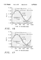
Refer now to FIG. 11, FIG. 16, and FIG. 17, there is shown another embodiment of this invention. This embodiment, as shown in FIG. 11, uses the compensating circuit of this invention in the closed loop sample and hold circuit. The closed loop sample and hold circuit is comprised of a first MOSFET 20 with the drain connected to the first terminal of an input resistor 22 and the first terminal of an input capacitor 23, the gate connected to the clock voltage 29, and the source connected to the first terminal of a holding capacitor 25 and the negative input of an operational amplifier connected for unity gain 26. The second terminal of the input resistor 22 and the second terminal of the input capacitor 23 are connected to the input voltage 21. The output 27 of the operational amplifier 26 is connected to the second terminal of the holding capacitor 25 and to the first terminal of a feedback resistor 24. The second terminal of the feedback resistor 24 is connected to the drain of the first MOSFET 20. The compensating circuit of this embodiment is the same as described in the previous embodiments. The third node 78 of the compensating circuit is connected to the source of the first MOSFET 20.
FIG. 16 shows computer simulation results of the conventional closed loop sample and hold circuit shown in FIG. 2 for a sinusoidal input voltage. FIG. 16 shows the input voltage 132 and output voltage 130 sampled at the switching points 127. FIG. 17 shows computer simulation results of the closed loop sample and hold circuit with the compensating circuit of this embodiment, shown in FIG. 11, using the same input and switching conditions as in the simulation results of the conventional closed loop sample and hold circuit. FIG. 17 shows the input voltage 136 and output voltage 134 sampled at the switching points 127. The error of the sampled output voltage can be seen to be much smaller in FIG. 17 than in FIG. 16.
While the invention has been particularly shown and described with reference to the preferred embodiments thereof, it will be understood by those skilled in the art that various changes in form and details may be made without departing from the spirit and scope of the invention.

Claims (20)

What is claimed is:
1. A circuit for compensating metal oxide semiconductor analog switches, comprising:
a first node;
a second node;
a third node;
a clock voltage signal;
a metal oxide semiconductor field effect transistor having a source, a drain, and a gate wherein said gate is connected to said clock voltage signal, said source is connected to said first node, and said drain is connected to said second node;
a complimentary metal oxide semiconductor field effect transistor inverting amplifier having an input and an output wherein said input of said complimentary metal oxide semiconductor field effect transistor inverting amplifier is connected to said first node and said output of said complimentary metal oxide semiconductor field effect transistor inverting amplifier is connected to said second node;
a first capacitor having a first terminal and a second terminal wherein said second terminal of said first capacitor is connected to said second node and said first terminal of said first capacitor is connected to said third node;
a second capacitor having a first terminal and a second terminal wherein said second terminal of said second capacitor is connected to said first node and said first terminal of said second capacitor is connected to said third node; and
a third capacitor having a first terminal and a second terminal wherein said first terminal of said third capacitor is connected to said first node and said second terminal of said third capacitor is connected to said second node.
2. The circuit of claim 1 wherein said first capacitor has a capacitance of at least 0.2 picofarads.
3. The circuit of claim 1 wherein said second capacitor has a capacitance of at least 0.2 picofarads.
4. The circuit of claim 1 wherein said third capacitor has a capacitance of at least 0.2 picofarads.
5. The circuit of claim 1 wherein said complimentary metal oxide semiconductor field effect transistor inverting amplifier has a gain of at least 30 dB.
6. A circuit having Compensation for a metal oxide semiconductor analog switch, comprising:
a first node;
a second node;
a third node;
a clock voltage signal;
a ground node;
an input node;
an output node;
a first metal oxide; semiconductor field effect transistor having a source, a drain, and a gate wherein said gate of said first metal oxide semiconductor field effect transistor is connected to said clock voltage signal, said source of said first metal oxide semiconductor field effect transistor is connected to said first node, and said drain of said first metal oxide semiconductor field effect transistor is connected to said second node;
a complimentary metal oxide semiconductor field effect transistor inverting amplifier having an input and an output wherein said input of said complimentary metal oxide semiconductor field effect transistor inverting amplifier is connected to said first node and said output of said complimentary metal oxide semiconductor field effect transistor inverting amplifier is connected to said second node;
a first capacitor having a first terminal and a second terminal wherein said second terminal of said first capacitor is connected to said second node and said first terminal of said first capacitor is connected to said third node;
a second capacitor having a first terminal and a second terminal wherein said second terminal of said second capacitor is connected to said first node and said first terminal of said second capacitor is connected to said third node;
a third capacitor having a first terminal and a second terminal wherein said first terminal of said third capacitor is connected to said first node and said second terminal of said third capacitor is connected to said second node;
a second metal oxide semiconductor field effect transistor having a source, a drain, and a gate wherein said gate of said second metal oxide semiconductor field effect transistor is connected to said clock voltage signal, said drain of said second metal oxide semiconductor field effect transistor is connected to said input node, and said source of said second metal oxide semiconductor field effect transistor is connected to said third node;
a holding capacitor having a first terminal and a second terminal wherein said first terminal of said holding capacitor is connected to said third node and said second terminal of said holding capacitor is connected to said ground node; and
an operational amplifier having a positive input, a negative input, and an amplifier output wherein said positive input of said operational amplifier is connected to said third node, said negative input of said operational amplifier is connected to said output node and said amplifier output of said operational amplifier is connected to said output node.
7. The circuit of claim 6 wherein said first capacitor has a capacitance of at least 0.2 picofarads.
8. The circuit of claim 6 wherein said second capacitor has a capacitance of at least 0.2 picofarads.
9. The circuit of claim 6 wherein said third capacitor has a capacitance of at least 0.2 picofarads.
10. The circuit of claim 6 wherein said complimentary metal oxide semiconductor field effect transistor inverting amplifier has a gain of at least 30 dB.
11. A circuit having compensation for a metal oxide semiconductor analog switch, comprising:
a first node;
a second node;
a third node;
a fourth node;
a fifth node;
a clock voltage signal;
a ground node;
an input node;
an output node;
a first metal oxide semiconductor field effect transistor having a source, a drain, and a gate wherein said gate of said first metal oxide semiconductor field effect transistor is connected to salad clock voltage signal, said source of said first metal oxide semiconductor field effect transistor is connected to said first node, and said drain of said first metal oxide semiconductor field effect transistor is connected to said second node;
a complimentary metal oxide semiconductor field effect transistor inverting amplifier having an input and an output wherein said input of said complimentary metal oxide semiconductor field effect transistor inverting amplifier is connected to said first node and said output of said complimentary metal oxide semiconductor field effect transistor inverting amplifier is connected to said second node;
a first capacitor having a first terminal and a second terminal wherein said second terminal of said first capacitor is connected to said second node and said first terminal of said first capacitor is connected to said third node;
a second capacitor having a first terminal and a second terminal wherein said second terminal of said second capacitor is connected to said first node and said first terminal of said second capacitor is connected to said third node;
a third capacitor having a first terminal and a second terminal wherein said first terminal of said third capacitor is connected to said first node and said second terminal of said third capacitor is connected to said second node;
a second metal oxide semiconductor field effect transistor having a source, a drain, and a gate wherein said gate of said second metal oxide semiconductor field effect transistor is connected to said clock voltage signal, said drain of said second metal oxide semiconductor field effect transistor is connected to said input node, and said source of said second metal oxide semiconductor field effect transistor is connected to said fifth node;
a third metal oxide semiconductor field effect transistor having a source, a drain, and a gate wherein said gate of said third metal oxide semiconductor field effect transistor is connected to said clock voltage signal, said drain of said third metal oxide semiconductor field effect transistor is connected to said fourth node, and said source of said third metal oxide semiconductor field effect transistor is connected to said third node;
a first operational amplifier having a positive input, a negative input, and a first amplifier output wherein said positive input of said first operational amplifier is connected to said ground node, said negative input of said first operational amplifier is connected to said third node and said first amplifier output of said first operational amplifier is connected to said fourth node;
a fourth capacitor having a first terminal and a second terminal wherein said first terminal of said fourth capacitor is connected to said fifth node and said second terminal of said fourth capacitor is connected to said fourth node;
a fifth capacitor having a first terminal and a second terminal wherein said first terminal of said fifth capacitor is connected to said fifth node and said second terminal of said fifth capacitor is connected to said third node; and
a second operational amplifier having a positive input, a negative input, and a second amplifier output wherein said positive input of said first operational amplifier is connected to said fifth node, said negative input of said second operational amplifier is connected to said output node and said second amplifier output of said second operational amplifier is connected to said output node.
12. The circuit of claim 11 wherein said first capacitor has a capacitance of at least 0.2 picofarads.
13. The circuit of claim 11 wherein said second capacitor has a capacitance of at least 0.2 picofarads.
14. The circuit of claim 11 wherein said third capacitor has a capacitance of at least 0.2 picofarads.
15. The circuit of claim 11 wherein said complimentary metal oxide semiconductor field effect transistor inverting amplifier has a gain of at least 30 dB.
16. A circuit having compensation for a metal oxide semiconductor analog switch, comprising:
a first node;
a second node;
a third node;
a fourth node;
a clock voltage signal;
a ground node;
an input node;
an output node;
a first metal oxide semiconductor field effect transistor having a source, a drain, and a gate wherein said gate of said first metal oxide semiconductor field effect transistor is connected to said clock voltage signal, said source of said first metal oxide semiconductor field effect transistor is connected to said first node, and said drain of said first metal oxide semiconductor field effect transistor is connected to said second node;
a complimentary metal oxide semiconductor field effect transistor inverting amplifier having an input and an output wherein said input of said complimentary metal oxide semiconductor field effect transistor inverting amplifier is connected to said first node and said output of said complimentary metal oxide semiconductor field effect transistor inverting amplifier is connected to said second node;
a first capacitor having a first terminal and a second terminal wherein said second terminal of said first capacitor is connected to said second node and said first terminal of said first capacitor is connected to said third node;
a second capacitor having a first terminal and a second terminal wherein said second terminal of said second capacitor is connected to said first node and said first terminal of said second capacitor is connected to said third node;
a third capacitor having a first terminal and a second terminal wherein said first terminal of said third capacitor is connected to said first node and said second terminal of said third capacitor i$ connected to said second node;
a second metal oxide semiconductor field effect transistor having a source, a drain, and a gate wherein said gate of said second metal oxide semiconductor field effect transistor is connected to said clock voltage signal, said drain of said second metal oxide semiconductor field effect transistor is connected to said fourth node, and said source of said second metal oxide semiconductor field effect transistor is connected to said third node;
a first resistor having a first terminal and a second terminal wherein said first terminal of said first resistor is connected to said input node and said second terminal of said first resistor is connected to said fourth node;
a shunt capacitor having a first terminal and a second terminal wherein said first terminal of said shunt capacitor is connected to said input node and said second terminal of said shunt capacitor is connected to said fourth node;
a feedback resistor having a first terminal and a second terminal wherein said first terminal of said feedback resistor is connected to said fourth node and said second terminal of said feedback resistor is connected to said output node;
an operational amplifier having a positive input, a negative input, and an amplifier output wherein said positive input of said operational amplifier is connected to said ground node, said negative input of said operational amplifier is connected to said output node and said amplifier output of said operational amplifier is connected to said output node; and
a holding capacitor having a first terminal and a second terminal wherein said first terminal of said holding capacitor is connected to said third node and said second terminal of said holding capacitor is connected to said output node.
17. The circuit of claim 16 wherein said first capacitor has a capacitance of at least 0.2 picofarads.
18. The circuit of claim 16 wherein said second capacitor has a capacitance of at least 0.2 picofarads.
19. The circuit of claim 16 wherein said third capacitor has a capacitance of at least 0.2 picofarads.
20. The circuit of claim 16 wherein said complimentary metal oxide semiconductor field effect transistor inverting amplifier has a gain of 7 at least 30 dB.
US08/394,771 1995-02-27 1995-02-27 Compensating circuit for MOSFET analog switches Expired - Lifetime US5479121A (en)

Priority Applications (1)

Application Number Priority Date Filing Date Title
US08/394,771 US5479121A (en) 1995-02-27 1995-02-27 Compensating circuit for MOSFET analog switches

Applications Claiming Priority (1)

Application Number Priority Date Filing Date Title
US08/394,771 US5479121A (en) 1995-02-27 1995-02-27 Compensating circuit for MOSFET analog switches

Publications (1)

Publication Number Publication Date
US5479121A true US5479121A (en) 1995-12-26

Family

ID=23560363

Family Applications (1)

Application Number Title Priority Date Filing Date
US08/394,771 Expired - Lifetime US5479121A (en) 1995-02-27 1995-02-27 Compensating circuit for MOSFET analog switches

Country Status (1)

Country Link
US (1) US5479121A (en)

Cited By (15)

* Cited by examiner, † Cited by third party
Publication number Priority date Publication date Assignee Title
US5838176A (en) * 1996-07-11 1998-11-17 Foveonics, Inc. Correlated double sampling circuit
WO1999039353A1 (en) * 1998-01-30 1999-08-05 Litef Gmbh Blanking circuit
US5977892A (en) * 1995-05-31 1999-11-02 Motorola, Inc. Offset cancellation circuit
WO2000014877A2 (en) * 1998-09-08 2000-03-16 Maxim Integrated Products, Inc. Constant gate drive mos analog switch
US6052000A (en) * 1997-04-30 2000-04-18 Texas Instruments Incorporated MOS sample and hold circuit
US6069502A (en) * 1998-04-06 2000-05-30 Intersil Corporation Sample-and-hold circuit having reduced subthreshold conduction effects and related methods
US20030020530A1 (en) * 2001-07-27 2003-01-30 Lee Wing Foon Method for nulling charge injection in switched networks
US6566934B1 (en) 2001-12-31 2003-05-20 International Business Machines Corporation Charge cancellation circuit for switched capacitor applications
WO2004001763A1 (en) * 2002-06-25 2003-12-31 Zarlink Semiconductor (U.S.) Inc. Sample and hold circuit
US6781434B2 (en) 2000-12-28 2004-08-24 Intel Corporation Low charge-dump transistor switch
US6970031B1 (en) * 2004-05-28 2005-11-29 Hewlett-Packard Development Company, L.P. Method and apparatus for reducing charge injection in control of MEMS electrostatic actuator array
US20080252358A1 (en) * 2007-04-11 2008-10-16 Texas Instruments Incorporated Circuit and method for reducing charge injection and clock feed-through in switched capacitor circuits
US7612586B1 (en) * 2007-10-24 2009-11-03 Advasense Technologies (2004) Ltd. Low noise analog sampling circuit and a method for low noise sampling of an analog signal
US20110181334A1 (en) * 2010-01-28 2011-07-28 Hung-Chieh Tsai Track and hold circuit and related receiving device with track and hold circuit employed therein
EP3806334A1 (en) 2019-10-07 2021-04-14 IniVation AG Switched capacitor circuit

Citations (11)

* Cited by examiner, † Cited by third party
Publication number Priority date Publication date Assignee Title
US3969636A (en) * 1975-06-30 1976-07-13 General Electric Company Charge sensing circuit for charge transfer devices
SU739549A1 (en) * 1977-10-25 1980-06-05 Харьковский авиационный институт Operational amplifier with compensation of zero level drift
EP0046549A1 (en) * 1980-08-27 1982-03-03 Siemens Aktiengesellschaft Output stage of a monolithic integrated charge-transfer device
JPS5760593A (en) * 1980-09-26 1982-04-12 Hitachi Ltd Sample holding circuit
JPS58169396A (en) * 1982-03-31 1983-10-05 Hitachi Ltd Sampling holding circuit
JPS5996599A (en) * 1982-11-22 1984-06-04 Sanyo Electric Co Ltd Sample hold circuit
US4604584A (en) * 1985-06-10 1986-08-05 Motorola, Inc. Switched capacitor precision difference amplifier
JPS6396800A (en) * 1986-10-13 1988-04-27 Sony Corp Cmos sample/hold circuit
US4894620A (en) * 1988-04-11 1990-01-16 At&T Bell Laboratories Switched-capacitor circuit with large time constant
WO1990003034A1 (en) * 1988-09-09 1990-03-22 Analog Devices, Inc. Sample-hold amplifier circuit
US5343089A (en) * 1990-01-26 1994-08-30 Kabushiki Kaisha Toshiba Sample-and-hold circuit device

Patent Citations (11)

* Cited by examiner, † Cited by third party
Publication number Priority date Publication date Assignee Title
US3969636A (en) * 1975-06-30 1976-07-13 General Electric Company Charge sensing circuit for charge transfer devices
SU739549A1 (en) * 1977-10-25 1980-06-05 Харьковский авиационный институт Operational amplifier with compensation of zero level drift
EP0046549A1 (en) * 1980-08-27 1982-03-03 Siemens Aktiengesellschaft Output stage of a monolithic integrated charge-transfer device
JPS5760593A (en) * 1980-09-26 1982-04-12 Hitachi Ltd Sample holding circuit
JPS58169396A (en) * 1982-03-31 1983-10-05 Hitachi Ltd Sampling holding circuit
JPS5996599A (en) * 1982-11-22 1984-06-04 Sanyo Electric Co Ltd Sample hold circuit
US4604584A (en) * 1985-06-10 1986-08-05 Motorola, Inc. Switched capacitor precision difference amplifier
JPS6396800A (en) * 1986-10-13 1988-04-27 Sony Corp Cmos sample/hold circuit
US4894620A (en) * 1988-04-11 1990-01-16 At&T Bell Laboratories Switched-capacitor circuit with large time constant
WO1990003034A1 (en) * 1988-09-09 1990-03-22 Analog Devices, Inc. Sample-hold amplifier circuit
US5343089A (en) * 1990-01-26 1994-08-30 Kabushiki Kaisha Toshiba Sample-and-hold circuit device

Non-Patent Citations (20)

* Cited by examiner, † Cited by third party
Title
"A High Speed Sample-and-Hold Technique Using A Miller Hold Capacitance," by Lim & Wooley, IEEE Journal of Solid State Circuits, vol. 26, No. 4, Apr. 1991, pp. 643-651.
"All-MOS Charge Redistribution Analog-to-Digital Conversion Techniques-Part I" by McCreary & Gray, IEEE Journal of Solid State Circuits, vol. SC-10, No. 6, Dec. 1975, pp. 371-379.
"An 8-Bit 50-MHz CMOS Subranging A/D converter with Pipelines Wide-Band S/H" by Ishikawa & Tosukahara, IEEE Journal of Solid State Circuits, vol. 24, No. 6, Dec. 1989, pp. 1485-1491.
"Charge Injection in Analog MOS Switches" by Wegmann et al, IEEE Journal of Solid State Circuits, vol. SC-22, No. 6, Dec. 1987, pp. 1091-1097.
"Dummy Transistor Compensation of Analog MOS Switches" by Eichenberger & Guggenbuhl, IEEE Journal of Solid State Circuits, vol. 24, No. 4, Aug. 1989, pp. 1143-1145.
"Measurement & Analysis of Charge Injection in MOS Analog Switches" by Shieh et al, IEEE Journal of Solid State Circuits, vol. SC-22, No. 2, Apr. 1987, pp. 277-281.
"Measurement & Modeling of Charge Feed Through in n-Channel MOS Analog Switches" by Wilson et al, IEEE Journal of Solid State Circuits, vol. SC-20, No. 6, Dec. 1985 pp. 1206-1212.
"New Observation of Charge Injection in MOS Analogue Switches" by Chen et al, Electronics Letters, vol. 30, No. 3, Feb. 3, 1994, pp. 213-214.
"On Charge Injection in Analog MOS Switches & Dummy Switch Compensation Techniques" by Eichenberger & Guggenbuhl, IEEE Transactions on Circuits And Systems, vol. 37, No. 2, Feb. 1990, pp. 256-264.
"Switch Induced Error Voltage on a Switched Capacitor" by Sheutthe, IEEE Journal of Solid State Circuits, vol. SC-19, No. 4, Aug. 1984, pp. 519-525.
A High Speed Sample and Hold Technique Using A Miller Hold Capacitance, by Lim & Wooley, IEEE Journal of Solid State Circuits, vol. 26, No. 4, Apr. 1991, pp. 643 651. *
All MOS Charge Redistribution Analog to Digital Conversion Techniques Part I by McCreary & Gray, IEEE Journal of Solid State Circuits, vol. SC 10, No. 6, Dec. 1975, pp. 371 379. *
An 8 Bit 50 MHz CMOS Subranging A/D converter with Pipelines Wide Band S/H by Ishikawa & Tosukahara, IEEE Journal of Solid State Circuits, vol. 24, No. 6, Dec. 1989, pp. 1485 1491. *
Charge Injection in Analog MOS Switches by Wegmann et al, IEEE Journal of Solid State Circuits, vol. SC 22, No. 6, Dec. 1987, pp. 1091 1097. *
Dummy Transistor Compensation of Analog MOS Switches by Eichenberger & Guggenbuhl, IEEE Journal of Solid State Circuits, vol. 24, No. 4, Aug. 1989, pp. 1143 1145. *
Measurement & Analysis of Charge Injection in MOS Analog Switches by Shieh et al, IEEE Journal of Solid State Circuits, vol. SC 22, No. 2, Apr. 1987, pp. 277 281. *
Measurement & Modeling of Charge Feed Through in n Channel MOS Analog Switches by Wilson et al, IEEE Journal of Solid State Circuits, vol. SC 20, No. 6, Dec. 1985 pp. 1206 1212. *
New Observation of Charge Injection in MOS Analogue Switches by Chen et al, Electronics Letters, vol. 30, No. 3, Feb. 3, 1994, pp. 213 214. *
On Charge Injection in Analog MOS Switches & Dummy Switch Compensation Techniques by Eichenberger & Guggenbuhl, IEEE Transactions on Circuits And Systems, vol. 37, No. 2, Feb. 1990, pp. 256 264. *
Switch Induced Error Voltage on a Switched Capacitor by Sheutthe, IEEE Journal of Solid State Circuits, vol. SC 19, No. 4, Aug. 1984, pp. 519 525. *

Cited By (22)

* Cited by examiner, † Cited by third party
Publication number Priority date Publication date Assignee Title
US5977892A (en) * 1995-05-31 1999-11-02 Motorola, Inc. Offset cancellation circuit
US5838176A (en) * 1996-07-11 1998-11-17 Foveonics, Inc. Correlated double sampling circuit
US6052000A (en) * 1997-04-30 2000-04-18 Texas Instruments Incorporated MOS sample and hold circuit
WO1999039353A1 (en) * 1998-01-30 1999-08-05 Litef Gmbh Blanking circuit
US6191639B1 (en) 1998-01-30 2001-02-20 Litef Gmbh Gating circuit for analog values
US6069502A (en) * 1998-04-06 2000-05-30 Intersil Corporation Sample-and-hold circuit having reduced subthreshold conduction effects and related methods
WO2000014877A2 (en) * 1998-09-08 2000-03-16 Maxim Integrated Products, Inc. Constant gate drive mos analog switch
WO2000014877A3 (en) * 1998-09-08 2000-06-08 Maxim Integrated Products Constant gate drive mos analog switch
US6781434B2 (en) 2000-12-28 2004-08-24 Intel Corporation Low charge-dump transistor switch
US6850098B2 (en) 2001-07-27 2005-02-01 Nanyang Technological University Method for nulling charge injection in switched networks
US20030020530A1 (en) * 2001-07-27 2003-01-30 Lee Wing Foon Method for nulling charge injection in switched networks
US6566934B1 (en) 2001-12-31 2003-05-20 International Business Machines Corporation Charge cancellation circuit for switched capacitor applications
WO2004001763A1 (en) * 2002-06-25 2003-12-31 Zarlink Semiconductor (U.S.) Inc. Sample and hold circuit
US6970031B1 (en) * 2004-05-28 2005-11-29 Hewlett-Packard Development Company, L.P. Method and apparatus for reducing charge injection in control of MEMS electrostatic actuator array
US20050264340A1 (en) * 2004-05-28 2005-12-01 Hewlett-Packard Development Company, L.P. Method and apparatus for reducing charge injection in control of mems electrostatic actuator array
US20080252358A1 (en) * 2007-04-11 2008-10-16 Texas Instruments Incorporated Circuit and method for reducing charge injection and clock feed-through in switched capacitor circuits
US7663424B2 (en) 2007-04-11 2010-02-16 Texas Instruments Incorporated Circuit and method for reducing charge injection and clock feed-through in switched capacitor circuits
US7612586B1 (en) * 2007-10-24 2009-11-03 Advasense Technologies (2004) Ltd. Low noise analog sampling circuit and a method for low noise sampling of an analog signal
US20110181334A1 (en) * 2010-01-28 2011-07-28 Hung-Chieh Tsai Track and hold circuit and related receiving device with track and hold circuit employed therein
US8575970B2 (en) * 2010-01-28 2013-11-05 Mediatek Inc. Track and hold circuit and related receiving device with track and hold circuit employed therein
EP3806334A1 (en) 2019-10-07 2021-04-14 IniVation AG Switched capacitor circuit
WO2021069278A1 (en) 2019-10-07 2021-04-15 Inivation Ag Switched capacitor circuit

Similar Documents

Publication Publication Date Title
US5479121A (en) Compensating circuit for MOSFET analog switches
EP0976198B1 (en) A method and device to convert an analog current to a digital signal
Lim et al. A high-speed sample-and-hold technique using a Miller hold capacitance
US4568917A (en) Capacitive digital to analog converter which can be trimmed up and down
Macq et al. A 10-bit pipelined switched-current A/D converter
US7532042B2 (en) Precision sampling circuit
US6724236B1 (en) Buffered bootstrapped input switch with cancelled charge sharing for use in high performance sample and hold switched capacitor circuits
JPH10312698A (en) Mos sample-and-hold circuit
US4779012A (en) Track-and-hold amplifier
US6850098B2 (en) Method for nulling charge injection in switched networks
US5384570A (en) Voltage storage circuits
Wu et al. A CMOS transistor-only 8-b 4.5-Ms/s pipelined analog-to-digital converter using fully-differential current-mode circuit techniques
JP2975378B2 (en) Track and hold circuit
US7173558B2 (en) Charge comparator with low input offset
EP0746093B1 (en) Operational amplifier
KR930007719B1 (en) Analog to digital converter circuit
US5812023A (en) Voltage offset compensation circuit
Gatti et al. An accurate CMOS sample-and-hold circuit
US6480065B1 (en) CMOS folding amplifier having high resolution and low power consumption
WO1992009990A1 (en) Method for clockfeedthrough error compensation in switched capacitor circuits
Huang et al. A high-accuracy CMOS oversampling switched-current sample/hold (S/H) circuit using feedforward approach
Xu et al. A CMOS Miller hold capacitance sample-and-hold circuit to reduce charge sharing effect and clock feedthrough
Pierce et al. Low-distortion correlated level shifting sample-and-hold stage
Caiulo et al. On the design of high-speed high-resolution track and holds
CN109936368B (en) Low-noise current mode open-loop sampling hold circuit and circuit module

Legal Events

Date Code Title Description
AS Assignment

Owner name: INDUSTRIAL TECHNOLOGY RESEARCH INSTITUTE, TAIWAN

Free format text: ASSIGNMENT OF ASSIGNORS INTEREST;ASSIGNORS:SHEN, WEI-CHEN;GU, YEN-BIN;LIN, CHU-CHANG;AND OTHERS;REEL/FRAME:007370/0126

Effective date: 19941230

STCF Information on status: patent grant

Free format text: PATENTED CASE

FPAY Fee payment

Year of fee payment: 4

FEPP Fee payment procedure

Free format text: PAYOR NUMBER ASSIGNED (ORIGINAL EVENT CODE: ASPN); ENTITY STATUS OF PATENT OWNER: LARGE ENTITY

Free format text: PAYER NUMBER DE-ASSIGNED (ORIGINAL EVENT CODE: RMPN); ENTITY STATUS OF PATENT OWNER: LARGE ENTITY

FPAY Fee payment

Year of fee payment: 8

FPAY Fee payment

Year of fee payment: 12