US5499248A - Test vector generator comprising a decompression control unit and a conditional vector processing unit and method for generating a test vector - Google Patents
Test vector generator comprising a decompression control unit and a conditional vector processing unit and method for generating a test vector Download PDFInfo
- Publication number
- US5499248A US5499248A US08/189,200 US18920094A US5499248A US 5499248 A US5499248 A US 5499248A US 18920094 A US18920094 A US 18920094A US 5499248 A US5499248 A US 5499248A
- Authority
- US
- United States
- Prior art keywords
- sequence
- memory
- pin
- terminals
- counter
- Prior art date
- Legal status (The legal status is an assumption and is not a legal conclusion. Google has not performed a legal analysis and makes no representation as to the accuracy of the status listed.)
- Expired - Lifetime
Links
Images


Classifications
-
- G—PHYSICS
- G11—INFORMATION STORAGE
- G11C—STATIC STORES
- G11C29/00—Checking stores for correct operation ; Subsequent repair; Testing stores during standby or offline operation
- G11C29/56—External testing equipment for static stores, e.g. automatic test equipment [ATE]; Interfaces therefor
-
- G—PHYSICS
- G01—MEASURING; TESTING
- G01R—MEASURING ELECTRIC VARIABLES; MEASURING MAGNETIC VARIABLES
- G01R31/00—Arrangements for testing electric properties; Arrangements for locating electric faults; Arrangements for electrical testing characterised by what is being tested not provided for elsewhere
- G01R31/28—Testing of electronic circuits, e.g. by signal tracer
- G01R31/317—Testing of digital circuits
- G01R31/3181—Functional testing
- G01R31/319—Tester hardware, i.e. output processing circuits
- G01R31/31917—Stimuli generation or application of test patterns to the device under test [DUT]
- G01R31/31919—Storing and outputting test patterns
- G01R31/31921—Storing and outputting test patterns using compression techniques, e.g. patterns sequencer
-
- G—PHYSICS
- G01—MEASURING; TESTING
- G01R—MEASURING ELECTRIC VARIABLES; MEASURING MAGNETIC VARIABLES
- G01R31/00—Arrangements for testing electric properties; Arrangements for locating electric faults; Arrangements for electrical testing characterised by what is being tested not provided for elsewhere
- G01R31/28—Testing of electronic circuits, e.g. by signal tracer
- G01R31/317—Testing of digital circuits
- G01R31/3181—Functional testing
- G01R31/31813—Test pattern generators
-
- G—PHYSICS
- G01—MEASURING; TESTING
- G01R—MEASURING ELECTRIC VARIABLES; MEASURING MAGNETIC VARIABLES
- G01R31/00—Arrangements for testing electric properties; Arrangements for locating electric faults; Arrangements for electrical testing characterised by what is being tested not provided for elsewhere
- G01R31/28—Testing of electronic circuits, e.g. by signal tracer
- G01R31/317—Testing of digital circuits
- G01R31/3181—Functional testing
- G01R31/319—Tester hardware, i.e. output processing circuits
- G01R31/31917—Stimuli generation or application of test patterns to the device under test [DUT]
- G01R31/31926—Routing signals to or from the device under test [DUT], e.g. switch matrix, pin multiplexing
Definitions
- the present invention relates to an apparatus for testing an electronic device having at least one terminal, said apparatus including at least one terminal channel assigned to said terminal, or to a specific set of terminals.
- the invention relates to the structural concept used in an integrated circuit tester (IC tester), in a board tester, or like tester circuitry.
- IC tester integrated circuit tester
- the invention deals particularly with those designed to test memories, or integrated components with logic and memory functions, such as ASICs.
- Integrated circuit testers are, in general, provided to test the functionality of IC's prior to their insertion or installation in an assembly, such as soldering on a printed circuit board. If any malfunction of an IC were only detectable on the board level (e.g., by a board tester), there would be a need to throw away the complete board, or at least the need for costly measures would arise, such as removal of the defective IC. Thus, integrated circuit testers ensure that defective IC's are detected in an early stage of assembly. This aspect is becoming more and more important with increasing integration, i.e., increasing package density of semiconductor chips.
- integrated circuit testers comprise logic circuitry which is dedicated to a specific terminal (pin) of the device to be tested (the so-called “Device under Test” or "DUT").
- DUT Device under Test
- the same kind of logic circuitry exists multiple times in an IC tester, once for every pin of the DUT. If the IC tester is set up to test DUT's with a given maximum n of pins, this means that the pin circuitry has to be provided n times: n can approximate several hundred or even exceed some thousand, in view of state-of-the-art semiconductor chips and the related packaging technology.
- the pin circuitry commonly comprises driver circuits for the assigned pin, and mostly also formatter and comparator circuits.
- the latter are circuits which combine data and timing information (formatter), or test a signal received from the assigned terminal for its timing and correct logic state (comparator).
- EP-B-329 798 and European Patent Application . . . application number: 91119190.6 which disclose formatters of the kind discussed herein, and to DE-C-33 46 942, EP-B-325 670 and European Patent Application . . . (application number: 91119165.8), as far as comparators are concerned.
- Shared resource in this context means that the control circuitry, or part thereof, is shared between multiple pins.
- the control circuitry may be provided only once, and communicate with the pin channels (terminal channels) via a common bus. This eliminates the need to replicate the control circuit for every pin of the DUT.
- it implies several design constraints, particularly speed constraints.
- the "per pin resource” approach provides control circuitry, or at least the speed-critical part thereof, for every pin channel. This approach may overcome the above speed restrictions; however, it may be very expensive as the control circuitry has to be provided n times. Sometimes even the speed of a "per pin” resource does not fit the requirements of a particular application.
- APG central algorithmic pattern generator
- the controller of such a prior art APG includes a programmable memory which contains the sequences to be generated, or a program which generates such sequences.
- a tester designed essentially according to the "shared resource” approach is, for example, disclosed in U.S. Pat. No 4,450,560.
- LSI testers logic testers
- a so-called sequencer (basically a counter with some additional control circuitry, such that it can perform jumps, subroutines etc.) generates addresses which are fed to a memory.
- the formatter processes the data received from the Vector Memory and links them with timing information, usually produced by edge generators.
- the comparator checks data produced by the DUT for their accuracy in timing, as well as their correct logic state. Both the formatter and the comparator are connected with a single pin of the device under test.
- Board testers are provided either to test blank boards--i.e., unloaded boards wherein only the electrical connections are of interest--, or loaded boards. Whereas the first case is trivial, the second requires extensive testing circuitry, as the components on the boards may fulfil a variety of functions. It will be appreciated that a board tester in this sense may be even more complex than an integrated circuit tester, as a board may be loaded with components of different technology, e.g., digital logic circuitry, memories, analog circuitry and the like. Thus, there is also a need for a board tester which is sufficiently fast and can test all the functions on the board, at a reasonable price.
- a sequence controller for generating a first sequence of vectors
- At least one decompression control unit which is controlled by the sequence controller, generates decompressed signals and feeds them to the sequence controller,
- sequence controller further includes conditional vector processing means for generating a second sequence of vectors in dependence of the first sequence of vectors, and independence of the decompressed signals received from the decompression control unit.
- a sequencer is a relatively cheap component which can easily be provided multiple times.
- the APG required for memory testing is extremely complex and expensive, such that a tester incorporating several hundreds of conventional APG's could hardly be commercialized.
- This is partially due to the fact that a sequencer generates single addresses only which are useful for all the "per pin” Vector Memories in a logic tester, whereas an APG generates x and y addresses for all cells of a memory, although in a "per pin” architecture, only a single bit would be required. In other words, a "per pin APG" structure would result in an enormous overhead.
- a sequence controller for generating a first sequence of vectors.
- This sequence controllers may be of conventional design; i.e., it is a relatively straight forward and cheap component.
- the decompression control unit receives control signals, or control patterns, from the sequence controller. These control signals are processed by the decompression control unit, preferably basically independent of the sequence controller.
- the decompression Control unit runs with its own clock, such that the sequence controller, once it has loaded the decompression control unit with the start-up parameters, has not to perform any supervisory tasks relating to the decompression control unit.
- the decompression control unit thus prepares signals (the meaning of which will be discussed below) and relieves the sequence controller from the related operations.
- the sequence controller further includes conditional vector processing means.
- the first sequence of vectors generated by the sequence controller is fed to this conditional vector processing means, as well as the decompressed signals received from the decompression control unit.
- the conditional vector processing means now generates a second sequence of vectors, in dependence of the signals fed to it, namely the first sequence of vectors, as well as the decompressed signals.
- a typical example of this kind of operation is when the first sequence of vectors consists of two or more different sub-sequences which are generated simultaneously.
- the decompressed signal determines which of said sub-sequences is fed to the output of the sequence controller. Formally, this corresponds to an instruction like "move A or B to output dependent on C", wherein A and B are the sub-sequences, and C is the decompressed signal.
- the conditional vector processing means may also perform other or related functions, such as gating the first sequence of vectors, performing any kind of logic combination between the first sequence of vectors and the decompressed signal, and the like.
- the basic advantage of this structure is a considerable increase in speed, at virtually no additional costs other than those for the decompression control unit (which may be of quite simple design).
- a sequence controller of basically the same or similar structure as known sequencers may be used.
- the decompression control unit relieves the sequence controller from some time-consuming tasks such as address generation (see discussion below).
- the sequence controller has to provide only the necessary startup conditions, and may further, from time to time, feed additional control information to the decompression control unit, in order to influence its operation.
- operation of the decompression control unit consumes basically no computational or logic power of the sequencer.
- the decompression control unit is basically self-operating and needs only some control information which defines the boundary conditions.
- the decompression control unit may be a separate component, it can also be integrated with the sequence controller, e.g., on the same chip.
- the decompression control unit expands control signals received from the sequence controller to decompressed signals.
- the conditional vector processing means may execute instructions with a conditional operand, wherein the condition of said conditional operand is set by the decompressed signals received from the decompression control unit.
- the invention is particularly suited for application in an integrated circuit tester.
- the integrated circuit contains at least a memory section and has a multiplicity of terminals or pins, wherein at least a first subset of said pins is at least temporarily operative as address pins, and at least a second subset of said pins is at least temporarily operative as data pins.
- This wording includes integrated circuits which are mixed logic/memory circuits, as well as pure memories, or pure logic.
- a terminal channel of the kind discussed at the outset may preferably be provided for essentially all pins of the second subset of pins, i.e., for the address pins.
- a sequence controller including the associated decompression control unit, is provided essentially for all address pins.
- terminal channels of the kind discussed above may also be provided for other pins, such as data pins, control pins, logic pins, analog pins and the like.
- the decompression control unit uses the startup and boundary conditions set by the sequencer to generate a train of complete (i.e., expanded) signals such as addresses.
- decompression control units are address generators, data generators, control byte generators, status byte generators and the like. Some of these, in particular the address generator, will be discussed in more detail below.
- the decompression control unit feeds the decompressed signals back to the sequencer, thus relieving the sequencer from the basically simple, but very time-consuming task of generating the vectors required to operate on the assigned pin of the DUT.
- the sequencer is able to control the assigned pin in real time even at very high testing speed. It is just this very concept which makes the inventive "multiple sequencer" structure suited for memory testing.
- the unique sequencer/decompression control unit combination according to this invention constitutes, in effect, a partial APG, namely an APG adapted to a specific pin of the DUT.
- the decompression control unit according to the invention generates preferably 1-bit information, in particular a 1-bit address, which is fed back to the sequencer (although the invention is not limited to this aspect).
- the sequencer operates preferably also in 1-bit mode, as it has to control a single pin only. This makes its operation very fast, particularly as signal decompression (e.g., address generation) is performed by fast hardware and thus requires no extra computational time to be spent by the sequencer.
- the invention establishes a new kind of memory tester. In fact, it is suited to test integrated circuit devices which contain only memories at very high speed. It does not need a multiplicity of expensive hardware, like the above discussed switch matrix or an APG per pin, such that it may be sold at attractive pricing.
- the various sequencers all execute different programs, in dependence of their assigned pin. However, in logic test mode, they may all execute the same program (as in prior art logic testers), although this is not a necessary condition for practicing the present invention.
- a Vector Memory decoder memory
- all sequencers may execute the same program, provided their respective Vector Memories have been loaded with data specific to the assigned pin.
- This embodiment has the advantage that the Vector memories may be easily reloaded in case a pin changes its definition, either during operation of an IC, or between different IC's.
- the invention also features a second memory (the Waveform memory), as disclosed in European Patent Application . . . (application no. 91119189.8), with the advantages described in this document.
- formatter/comparator circuits of the kind described above are interconnected between the sequence controller and the assigned pin of the DUT, or a buffer (preferably a first-in-first-out memory) is provided between the sequence controller and the decoder memory.
- pin channels pin circuits
- the pin channels may not only be used to drive the address pins (in memory testing mode, or if set up for pure memory testing), or the logic pins (in logic testing mode) of the device under test.
- it may be used to drive data pins (in memory test mode), control pins (in either mode) and basically any other kind of pin of the DUT as well!
- an integrated circuit tester may be set up such that it drives basically all pins of the DUT, regardless of their functionality, with the same circuitry, namely with pin driver circuits according to this invention. It will be appreciated that this makes hardware configuration, storage keeping etc. particularly easy (and inexpensive), as only one kind of pin driver has to be provided. However, it will be understood that the present invention covers also cases wherein only a specific subset of the pins, e.g. only the data pins, of a DUT are driven by the inventive pin circuitry.
- a central controller which is connected with essentially all of the sequence controllers, said central controller controlling the contents of an instruction memory which is part of every sequencer.
- the controller may be set up to synchronize the various pin channels, provide control information to the "per pin" sequencers, collect test results etc.; however, it will not be actually involved in the time-critical test sequences which are performed locally.
- the central controller may be adapted to load each sequence controller's instruction memory with instructions specifically dedicated to its assigned pin. This is an important feature to increase the variability of the tester.
- the central controller may easily exchange, i.e., download, the instruction sets in the memories of the various sequencers in case a pin definition changes.
- the central controller may also be programmed to generate different instructions from an overall test procedure for every assigned pin. That is, the "overall" test pattern is only known to the central controller, which transforms it into a multiplicity of simpler, pin-dedicated test programs which are then downloaded to and executed by the sequencers.
- a sequence controller is assigned to basically every pin of the DUT, at least to those pins which may permanently or from time to time, be operated as address pins.
- the sequence controllers may be basically of the same or similar structure as known sequencers. This is a novel approach for a memory or logic/memory tester, although already known in pure logic testers. It is also surprising because nobody skilled in the art would have expected that a sequencer, although designed to generate addresses for logic testing, could be useful for memory testing as well.
- the decompression control unit may be, or include, an address generator (in particular a 1-bit address generator).
- address generators may, for example, feature a frequency divider (e.g., flip-flops with a feedback loop), shift registers and the like.
- a frequency divider e.g., flip-flops with a feedback loop
- shift registers e.g., shift registers and the like.
- at least one counter or a chain of counters
- N-pattern One of the most simple test patterns used in memory testing is the so-called "N-pattern".
- N address generation cycles wherein N is the total number of memory cells.
- N address generation cycles wherein N is the total number of memory cells.
- other N address generation cycles that is, we have a total number of 2N address generation cycles.
- N 2 -pattern Another, more sophisticated way of memory testing is the so-called “N 2 -pattern”. It uses a concept of "home cells” and “away cells”. For example, the content of one cell in the memory (the home cell) is held constant, whereas all other cells in the memory (the away cells) are varied, in order to check whether the contents of the home cell are influenced by any transition in the away cells. This process is continued until all cells of the memory have operated as "home cells” once.
- a decompression control unit particularly suited for this kind of memory testing includes
- a first counter set up to generate at least the address bit of the assigned terminal of the address of at least one first memory cell the content of which is held constant during a test cycle
- a second counter set up to generate at least the address bit of the assigned terminal of the address of at least one second memory cell the content of which is varied during a test cycle.
- the first counter generates the address of the home cell(s), whereas the second counter generates the address of the away cell(s). If we take the first example with a single home cell, the first counter (which points to the home cell) will thus have a long period, and the second counter (which points to the away cells) will have a short period. The first counter will be held at a constant value, whereas the second counter counts through all cells of the memory. As soon as the second counter approaches the last cell in the memory, it is reset, whereas the first counter is increased by one thus defining the next home cell, and so on.
- the whole process runs under control of the sequencer, which may start, stop and control the two counters, e.g. by controlling the "HOLD/RUN" inputs of the counters, their preset inputs or their clock inputs.
- the counters may (at least partially) also control each other; in the above-described example, the second counter could e.g. provide a carry bit which would increment the first counter.
- This embodiment incorporating two counters is particularly effective upon memory testing, because the counters remove most of the time-consuming "standard” work (multiple address generation) from the sequencer and thus increase its operating speed considerably.
- the third counter may provide the necessary information therefore; that is, as soon as it has reached its final state, the sequencer will disregard one address generated by the second counter (preferably, by simple not advancing the corresponding vector to a buffer). It will be understood that this is functionality which could also be provided by the sequencer; however, use of a third counter is more effective and illustrates once more the outstanding advantages of the present invention.
- N 2 -pattern is quite effective in testing; however, it may lead to considerable test times (sometimes exceeding one hour per memory). Thus, other patterns--which need less time for processing--should be regarded as well.
- One important groups of these patterns is the so-called "N 3/2 -pattern". It is based on the finding that it may be sufficient (without considerable loss of performance) to keep to the "home cell” approach, but use only cells in the same row or column as away cells. A specific example of this group, the butterfly pattern, will now be discussed in greater detail.
- the first away cells tested are--by definition--the memory cells closest to the home cell and in the same row or column as the home cell. These are four cells.
- the distance to the home cell is increased by 1, resulting in four further away cells, and so on.
- This pattern is usually processed in clockwise or counter-clockwise direction and requires to test 2 ⁇ ( ⁇ N-1) away cells (assuming a "square" memory).
- N times for N home cells
- a counter structure of the decompression control unit is also suited to produce the addresses of such a butterfly pattern (and any other kind of N 3/2 -pattern).
- one counter can be used as a row counter, and the other as a column counter, if they are set to different periods (because each row/column has another assigned weighting).
- a slightly modified counter structure may advantageously be used.
- one counter is set up as "home counter” which points to the home cell.
- Two away counters operate in “increment” and “decrement” mode for the assigned row, i.e., they represent an offset with regard to the home cell. Their contents may be fed to the sequencer, in order to calculate the actual address of the away cells in the same row as the home cell.
- speed may further be increased by the provision of external adders which add the contents of the "home” counter and the "away” counters, respectively.
- the same structure (two away counters, adders) may be repeated for the column assigned to the home cell.
- the present invention also relates to a method for testing an electronic device.
- FIG. 1 is a structural diagram of a prior art memory tester
- FIG. 2 depicts the structure of a prior art logic tester using the "shared resource” approach
- FIG. 3 shows another prior art logic tester based on the "per pin" architecture
- FIG. 4 depicts the overall embodiment of a tester according to the present invention
- FIG. 5 shows a pin circuitry according to the invention in greater detail
- FIGS. 6 and 7 are diagrams illustrating operation when a memory is tested with an N 2 -pattern
- FIG. 8 depicts an N 3/2 -pattern, namely the butterfly pattern
- FIG. 9 shows a pin circuitry specifically adapted to perform an N 3/2 -pattern.
- the prior art memory tester shown in FIG. 1 includes an algorithmic pattern generator (APG) 1 which serves as a common resource for a multiplicity of pin circuits.
- APG 1 consists basically of four functional units. One is an x address generator 2, the second is a y address generator 3, block 4 represents the data generator, and block 5 the controller. Address generators 2 and. 3 are provided for addressing a certain cell of the memory under test, whereas data generator 4 produces the data to be stored under the addressed memory cell.
- Functional block 5 controls operation of the address generators and the data generator.
- the output signals of APG 1 are fed to a common bus 6.
- the bus is connected with a multiplicity of pin channels or pin circuits, represented in FIG. 1 by pin boards 7a, 7b and 7c. It will be understood that three pin boards have been drawn for purposes of illustration only, whereas a real memory tester would include several hundred, or even several thousands of pin boards.
- DUT device under test
- pin boards 7a to 7c The major purpose of pin boards 7a to 7c is to link the information received via common bus 6 with timing signals usually received from edge generators, as indicated by arrows 10a, 10b and 10c.
- the pin boards include circuitry to link information received from APG 1 with timing information (formatter circuits), as well as circuitry designed to test the correct timing, and the correct logic state, of signals received from DUT 8 (comparator circuits).
- Algorithmic pattern generator 1 is a very complex and expensive unit. This is the reason why a single APG is provided for all of the pin boards (shared resource approach). This limits testing speed considerably. It will further be noted that the pin boards 7a to 7c may be different, dependent on the functionality of the assigned pin of DUT 8 (i.e., whether this pin is an address pin, a data pin or a control pin). Thus, a complex and time-consuming rearrangement of the pin boards and their interconnection is necessary as soon as the pin definition of DUT 8 is changed. This is the reason why the structure shown in FIG. 1 is mainly suited to test memories of the same kind.
- FIG. 2 depicts another approach of a prior art IC tester, namely a logic tester. This logic tester is also based on the "shared resource approach”.
- a sequencer 11 generates vector addresses which are fed, via a common bus 12, to the various pin channels or pin boards.
- Sequencer 11 is, in functional terms, a counter; however, it comprises additional circuitry such that it is able to perform jumps, subroutines and the like.
- sequencer 11 may also include a memory which defines some kind of program to be executed by the sequencer.
- sequencer 11 is of essentially simpler structure than the APG used in memory testing.
- the output signals of sequencer 11 are fed, via bus 12, to vector memories 13a, 13b and 13c assigned to the pin channels (again, it will be noted that an actual logic tester will contain hundreds or even thousands of such pin channels).
- the vector memory decodes basically the address received from sequencer 11 into a status information, or actions, to be performed by the assigned pin of DUT 16 (in this case, a logic circuit).
- vector memories 13a to 13c are fed to formatter/comparator circuitry 14a to 14c. These receive timing signals (arrows 15a to 15c).
- a more sophisticated approach is the additional provision of a waveform memory between every vector memory and the assigned formatter/comparator circuit.
- Such a waveform memory as disclosed in European patent application . . . (application number 91119189.8) allows to decode a variety of possible actions and thus increases the test spectrum.
- the logic tester shown in FIG. 2 is less complex than the memory tester discussed in the preceding figure. This does not only apply to the sequencer which is not as complex as the APG of a memory tester; it will also be noted that a logic device under test (DUT 16) does not comprise address pins and data pins, such that a complex rearrangement of the pin boards is not necessary.
- vector memory 13a will usually be incorporated on the same pin board as formatter/comparator circuitry 14a, as is the case for all other vector memory-formatter/comparator combinations.
- the design shown in FIG. 2 is subject to the same or similar constraints in timing as the memory tester shown in FIG. 1.
- the sequencer required for logic testing is of less complicated design, it is possible--at reasonable cost--to provide a single sequencer for every pin of the device under test.
- FIG. 3 This approach, also called “per pin approach”, is depicted in FIG. 3.
- the logic tester shown in this figure includes a multiplicity of sequencers 11a, 11b and 11c, all assigned to a specific pin channel.
- the remaining components of the tester shown in FIG. 3 are basically identical to the tester of FIG. 2 and have thus been assigned the same reference numbers.
- each pin channel includes a sequencer 17a, 17b, 17c; a decompression control unit 18a, 18b, 18c; a vector memory 19a, 19b, 19c; and formatter/comparator circuitry 20a, 20b, and 20c.
- the DUT 21 may be a memory, or an integrated circuit incorporating logic and memory functions, such as an ASIC. DUT 21 may basically have any arbitrary pin configuration; in particular, there is no need to adapt a pin channel to an address pin, data pin or control pin. In other words, no hardware reconfiguration is necessary if the pin definition changes between various DUTs, or even if the pin channel definition changes during operation.
- Every sequencer or sequence controller 17a, 17b and 17c also includes an instruction memory 172', 17b' and 17c', as well as a buffer (first-in-first-out memories 17a", 17b" and 17c").
- a central controller 22 is connected with the various pin channels, either directly or via a common bus 23.
- sequencers 17a to 17c feed control instructions to decompression control units 18a to 18c via lines 25a to 25c.
- the expanded or decompressed signals (which were generated by decompression control units 18a to 18c) are fed back to the sequencers via lines 26a to 26c.
- pins 27a and 27b of DUT 21 are defined as address pins, whereas pin 27c is defined as a logic pin.
- DUT 21 includes a memory as well as additional logic circuitry.
- DUT 21 will also include data pins, and that further pins, like analog pins, may be provided as well.
- These pins may be controlled by similar pin circuitry as shown in FIG. 4; however, for graphical purposes, only two address pins, and a logic pin, are shown in the example of FIG. 4.
- Central controller 22 will now use the overall test program for the memory portion of DUT 21 to generate pin-designated subprograms which are fed, via common bus 23, to the instruction memories 17a' and 17b' of sequence controllers 17a and 17b, respectively. That is, the instructions fed to instruction memory 17a' are different from the instructions fed to instruction memory 17b', dependent on the weighting of the assigned address pin.
- Sequence controllers 17a and 17b will provide suitable control information to decompression control units 18a and 18b (via lines 25a and 25b). The control information will cause decompression control units 18a and 18b to generate pin-specific decompressed signals, e.g. addresses, in sequence and feed them, via lines 26a and 26b, to sequence controllers 17a and 17b.
- the sequence controllers generate internally a first sequence of vectors.
- the shown example depicts sequence controllers which even generate two subsequences which together constitute said first sequence.
- sequence controller 17a two boxes 28a and 28a' illustrate the generation of the two sub-sequences of said first sequence of vectors.
- the signal fed back from decompression control unit 18a on line 26a moves either sub-sequence to an internal buffer 29a, by operating a (hardware or software) multiplexer 30a.
- This structure has been chosen for illustrative purposes only and shows the operation of a "conditional operand". That is, either of the two sub-sequences generated in boxes 28a and 28a' is moved to box 29a, dependent on the condition set by decompression control unit 18a.
- conditional vector processing means need not necessarily be in the form of a multiplexer as illustrated by multiplexers 30a to 30c.
- conditional vector processing means may basically be any logic circuitry which connects the first sequence of vectors with the output signals of the decompression control unit, in order to generate a second sequence of vectors.
- a multiplexer or equivalent means may be provided with a multiplicity of inputs, instead of the two inputs per multiplexer shown in FIG. 4.
- sequence controllers 17a and 17b generate a train of signals which are fed to vector memories 19a and 19b.
- the vector memories may also be loaded by central controller with pin-specific data, as indicated by lines 31a, 31b and 31c.
- the address patterns are fed back to the sequence controller and, from buffers 17a" and 17b" via formatter/comparator circuits 20a and 20b, to pins 27a and 27b of DUT 21.
- sequence controller 17c generates logic signals.
- Decompression control unit 18c runs idle, or may be used to generate specific vector trains required for logic testing. For example, decompression control unit 18c may generate a train of address signals required in the process of addressing vector memory 19c.
- DUT 21 changes its pin definition during test in that pin 27a is redefined from an address pin to a data pin.
- central controller 22 will simply switch between program modules already downloaded in advance in instruction memory 17a' of sequence controller 17a, such that it can serve as a data pin controller, and operation can immediately continue.
- This is a reconfiguration of the pin definition "on the fly", i.e., without the necessity to download new instructions.
- the same procedure is followed if another DUT with a different pin definition is inserted. (Of course, one may also download new instructions into instruction memory 17a' to obtain the same result, but this requires additional time and is therefore the less preferred approach.)
- Central controller 22 may not only provide instruction codes to memories 17a' to 17c', or to vector memories 19a to 19c. Instead, it may also control the overall timing of the tester, e.g., ensure that the sequence controllers assigned to address pins start their operation at the same point in time when data pin channels become active.
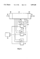
- FIG. 5 depicts part of a pin circuitry in greater detail. In particular, it shows one preferred embodiment of a decompression control unit.
- Sequencer 32 and its instruction memory 32' as well as its buffer 32" correspond basically to the sequence controllers shown in FIG. 4. Information from the central controller is received via line 33; the vector output is labelled as 34. The components succeeding sequence controller 32 in a pin channel are not drawn in FIG. 5.
- the decompression control unit consists, in the embodiment of FIG. 5, basically of three counters 35, 36 and 37. Their operation is controlled by the sequence controller 32; for example, sequence controller 32 controls the "HOLD/RUN” input (line 38) and the "PRESET” input (line 37) of counter 35. The other counters are controlled accordingly.
- counters 35 to 37 In particular, control of the start-up and boundary conditions, the counters are themselves free-running. That is, once they have received the necessary startup control codes, they will continue their operation on their own. Usually, they will receive a separate clock signal therefor, see clock generator 39 in FIG. 5. In certain cases, it may also be advisable to have some clock cycles directly controlled from the sequencer 32; in this case, the clock output of the sequencer, as well as the clock output of clock generator 39, will be fed to the inputs of a multiplexer, the output of which will be fed to the corresponding clock input of one of the counters.
- the addresses generated by counters 35 to 37 are fed, via lines 40, 41 and 42, to sequence controller 32.
- the sequence controller may link these addresses (which will usually be 1-bit addresses) with other control information, as explained above, or feed them directly to line 34.
- FIG. 6 depicts schematically a memory 43, in this case--for the sake of simplicity--consisting of 7 ⁇ 7 memory cells.
- the test is performed in that the content of one cell 44 is held constant, whereas the contents of all other cells are variable, as indicated by the character "v".
- the test reveals whether any transition in any cell of the memory except cell 44 influences the contents of the latter cell.
- cell 44 is designated as "home cell”, whereas the other cells are denominated as "away cells”.
- a complete test cycle consists of defining every cell of the memory as home cell, and of varying all away cells for every specific home cell. Thus, the number of test cycles necessary is proportional to N 2 , such that this kind of test is also known as "N 2 -test".
- the decompression control unit shown in FIG. 5 is perfectly suited to produce the addresses required for such an N 2 -test.
- counter 35 may point to the home cell, and counter 36 to a specific away cell.
- Counter 35 holds its value for a specific home cell, whereas counter 36 runs through all cells of the memory.
- counter 36 When counter 36 has reached its final state, it will be reset, and counter 35 will be incremented by one, thus pointing to the next home cell. This increment can be done by control logic incorporated in sequence controller 32, or even directly by feeding a carry bit of counter 36 to counter 35, as indicated by dotted line 45.
- the away counter 36 runs then again from 0 to its final state (or vice versa). The whole process is continued until all cells in the memory have acted as home cells.
- counter 37 Additional address information is provided by counter 37.
- away counter 36 should, during one cycle, point to all cells of memory 43 except the home cell 44 itself (as it would otherwise destroy the contents of the home cell). Thus, there is a need to skip one address in the memory.
- this task could be performed by internal control logic in sequence controller 32, it is easier to use an additional counter (namely counter 37) which causes sequence controller 32 to remove an address vector whenever the away counter points to the home cell. If that happens, sequence controller 32 simply does not advance the related address vector to buffer memory 32".
- counter 37 will run with a period of (N+1), wherein N is the total number of memory cells. In the example of FIG. 6, the period will be 50.
- FIG. 7 shows another N 2 -pattern which is somewhat the reverse of the pattern shown in FIG. 6.
- all cells in memory 61 are held constant with the exception of a cell 46 the contents of which are varied (character "v").
- the pattern in FIG. 7 includes (N-1) home cells, and a single away cell. It is evident that the three-counter structure of FIG. 5 is also suited to fit the needs of the test illustrated in FIG. 7.
- FIG. 8 depicts the example of a clockwise test. That is, the first array cell is the cell just above the home cell, as indicated by character "A”. Cells B, C and D are the next cells to be varied. The distance to the home cell is then increased by one, as indicated by cell E, and so on.
- the resulting pattern looks somewhat like a butterfly.
- the butterfly pattern is one specific example of the so-called "N 3/2 -tests", as the number of required test cycles is proportional to N 3/2 .
- FIG. 9 depicts a somewhat modified counter structure of the decompression control unit adapted to support N3/2-test patterns.
- Sequence controller 32, its instruction memory 32' and buffer 32" are the same as in the embodiment of FIG. 5.
- Counter 49 points to the home cell (see reference number 47 in FIG. 8). Counter counts an offset increment with respect to the row in which the home cell is located. Similarly, counter 51 counts down (decrements) in the row of the home cell.
- the output of home cell counter 49 is fed, together with the output of row increment counter 50, to an adder 52.
- the output of this adder is, in turn, fed back to the sequence controller.
- the vector such received by the sequence controller points subsequently to all cells right of the home cell (e.g., cell B in FIG. 8).
- adder 53 adds the contents of home cell counter 49 and of row decrement counter 51, such that all away cells left from the home cell (such as cell D in FIG. 8) are addressed.
- counter 54 is a column increment counter, such that adder 55 produces an address which points to all away cells above the home cell (cells A, E in FIG. 8).
- Column decrement counter 56 feeds its output to adder 57, which produces a vector pointing to all memory cells below the home cell (cell C in FIG. 8).
- adders 52, 53, 55 and 57 are not a necessary prerequisite for practicing the present invention.
- the adding function is something which could also be provided by sequence controller 32. However, the adders increase processing speed further.
- the architecture shown in FIG. 9 may be used to support the above-described N 2 -test as well.
- counters 49, 50 and 54 could be used to provide the three addresses necessary therefor.
- they have also a direct feedback to sequence controller 32, as shown by lines 58, 59 and 60.
- counters 49, 50 and 51 operate as row and column increment/decrement counters, respectively. This can easily be done by reprogramming them, and saves hardware components; thus, it is in fact the presently preferred approach.
- counters 49, 50 and 51 would have a direct feedback, i.e., a duplex connection, with sequence controller 32, in order to support the N 2 -test as well (this is different from FIG. 9 which depicts no direct feedback from counter 51 to sequence controller 32).
- This alternative structure is thus quite similar to the embodiment of FIG. 5, but includes additional adders 52 and 53.
Abstract
Description
Claims (33)
Applications Claiming Priority (2)
| Application Number | Priority Date | Filing Date | Title |
|---|---|---|---|
| DE4305442.0 | 1993-02-23 | ||
| DE4305442A DE4305442C2 (en) | 1993-02-23 | 1993-02-23 | Method and device for generating a test vector |
Publications (1)
| Publication Number | Publication Date |
|---|---|
| US5499248A true US5499248A (en) | 1996-03-12 |
Family
ID=6481067
Family Applications (1)
| Application Number | Title | Priority Date | Filing Date |
|---|---|---|---|
| US08/189,200 Expired - Lifetime US5499248A (en) | 1993-02-23 | 1994-01-31 | Test vector generator comprising a decompression control unit and a conditional vector processing unit and method for generating a test vector |
Country Status (3)
| Country | Link |
|---|---|
| US (1) | US5499248A (en) |
| JP (1) | JP3577332B2 (en) |
| DE (1) | DE4305442C2 (en) |
Cited By (53)
| Publication number | Priority date | Publication date | Assignee | Title |
|---|---|---|---|---|
| US5696772A (en) * | 1994-05-06 | 1997-12-09 | Credence Systems Corporation | Test vector compression/decompression system for parallel processing integrated circuit tester |
| US5737512A (en) * | 1996-05-22 | 1998-04-07 | Teradyne, Inc. | Fast vector loading for automatic test equipment |
| WO1998029898A2 (en) * | 1996-12-19 | 1998-07-09 | Simd Solutions, Inc. | Scalable tester architecture with i-cached simd technology |
| US5805610A (en) * | 1997-04-28 | 1998-09-08 | Credence Systems Corporation | Virtual channel data distribution system for integrated circuit tester |
| US5825787A (en) * | 1997-11-25 | 1998-10-20 | Xilinx, Inc. | System and method for accessing a test vector memory |
| US5872797A (en) * | 1996-12-02 | 1999-02-16 | International Business Machines Corporation | Burn-in signal pattern generator |
| US5883905A (en) * | 1997-02-18 | 1999-03-16 | Schlumberger Technologies, Inc. | Pattern generator with extended register programming |
| US5883906A (en) * | 1997-08-15 | 1999-03-16 | Advantest Corp. | Pattern data compression and decompression for semiconductor test system |
| US5894484A (en) * | 1997-04-28 | 1999-04-13 | Credence Systems Corporation | Integrated circuit tester with distributed instruction processing |
| US5899961A (en) * | 1996-04-30 | 1999-05-04 | Hewlett-Packard Company | Electronic circuit or board tester with compressed data-sequences |
| WO1999023501A1 (en) * | 1997-10-31 | 1999-05-14 | Credence Systems Corporation | Integrated circuit tester having pattern generator controlled data bus |
| WO1999053330A1 (en) * | 1998-04-15 | 1999-10-21 | Teradyne, Inc. | High speed, real-time, state interconnect for automatic test equipment |
| US6018814A (en) * | 1997-03-26 | 2000-01-25 | Simd Solutions, Inc. | Star-I: scalable tester architecture with I-cached SIMD technology |
| US6067651A (en) * | 1998-02-20 | 2000-05-23 | Hewlett-Packard Company | Test pattern generator having improved test sequence compaction |
| US6131172A (en) * | 1998-02-20 | 2000-10-10 | Micron Electronics, Inc. | Method for classifying electronic devices |
| US6182262B1 (en) * | 1997-02-04 | 2001-01-30 | Micron Technology, Inc. | Multi bank test mode for memory devices |
| US6181616B1 (en) | 1998-09-03 | 2001-01-30 | Micron Technology, Inc. | Circuits and systems for realigning data output by semiconductor testers to packet-based devices under test |
| US6202179B1 (en) | 1997-05-09 | 2001-03-13 | Micron Technology, Inc. | Method and apparatus for testing cells in a memory device with compressed data and for replacing defective cells |
| EP1095287A1 (en) * | 1998-06-12 | 2001-05-02 | Credence Systems Corporation | Integrated circuit tester with amorphous logic |
| EP1125140A1 (en) * | 1998-10-28 | 2001-08-22 | Credence Systems Corporation | Integrated circuit tester with disk-based data streaming |
| EP1149294A1 (en) * | 1999-01-29 | 2001-10-31 | Credence Systems Corporation | Algorithmic pattern generator for integrated circuit tester |
| US6363022B2 (en) * | 2000-08-03 | 2002-03-26 | Advantest Corporation | Semiconductor memory device tester |
| US6374376B1 (en) | 1998-09-03 | 2002-04-16 | Micron Technology, Inc. | Circuit, system and method for arranging data output by semiconductor testers to packet-based devices under test |
| US6412087B1 (en) * | 1998-07-30 | 2002-06-25 | Ando Electric Co., Ltd. | Pattern data transfer circuit |
| US6560756B1 (en) * | 2001-07-02 | 2003-05-06 | Ltx Corporation | Method and apparatus for distributed test pattern decompression |
| US20030110427A1 (en) * | 2000-04-12 | 2003-06-12 | Advantest Corporation | Semiconductor test system storing pin calibration data in non-volatile memory |
| DE10159165A1 (en) * | 2001-12-03 | 2003-06-26 | Agilent Technologies Inc | Device for measuring and / or calibrating a test head |
| US6624646B2 (en) | 1999-08-23 | 2003-09-23 | Agilent Technologies, Inc. | Modular interface between test and application equipment |
| US6734759B2 (en) | 2001-12-05 | 2004-05-11 | Agilent Technologies, Inc. | Droop compensation filter having high pass characteristic |
| US20040255215A1 (en) * | 2003-06-12 | 2004-12-16 | Hildebrant Andrew S. | Systems and methods for adaptively compressing test data |
| US20050007266A1 (en) * | 2003-06-17 | 2005-01-13 | Jochen Rivoir | Sigma-delta modulator with PWM output |
| US20050025274A1 (en) * | 2003-02-25 | 2005-02-03 | Jochen Rivoir | Transition tracking |
| US20050097413A1 (en) * | 2003-10-17 | 2005-05-05 | Srivaths Ravi | System-level test architecture for delivery of compressed tests |
| EP1584937A1 (en) * | 2004-04-05 | 2005-10-12 | AGILENT TECHNOLOGIES, INC. (n. d. Gesetzen d. Staates Delaware) | Systems and methods for processing automatically generated test patterns |
| US20050246603A1 (en) * | 2004-05-03 | 2005-11-03 | Markus Rottacker | Pin coupler for an integrated circuit tester |
| US20050264278A1 (en) * | 2004-04-05 | 2005-12-01 | Agilent Technologies, Inc. | Device for releasable connecting an interface with a test equipment |
| US20060028364A1 (en) * | 2004-08-06 | 2006-02-09 | Jochen Rivoir | Analog signal generation using a delta-sigma modulator |
| EP1701173A1 (en) | 2005-03-11 | 2006-09-13 | Agilent Technologies, Inc. | Error detection in compressed data |
| US20070022349A1 (en) * | 2005-07-07 | 2007-01-25 | Agilent Technologies, Inc. | Test apparatus with tester channel availability identification |
| US20070126414A1 (en) * | 2004-06-24 | 2007-06-07 | Agilent Technologies, Inc. | Jitter generation |
| US20070150224A1 (en) * | 2004-07-07 | 2007-06-28 | Agilent Technologies, Inc. | Evaluation of an output signal of a device under test |
| US7279887B1 (en) * | 2004-08-06 | 2007-10-09 | Nvidia Corporation | In-process system level test before surface mount |
| EP1901472A2 (en) | 2005-04-29 | 2008-03-19 | Verigy (Singapore) Pte. Ltd. | Communication circuit for a bi-directional data transmission |
| US20080128695A1 (en) * | 2004-02-27 | 2008-06-05 | Schieck Brian S | Flip chip semiconductor die internal signal access system and method |
| US20090125290A1 (en) * | 2007-11-08 | 2009-05-14 | Prosenjit Chatterjee | Automatic verification of device models |
| US20090210759A1 (en) * | 2008-02-14 | 2009-08-20 | Nvidia Corporation | Scalable Scan-Based Test Architecture With Reduced Test Time And Test Power |
| US20090282143A1 (en) * | 2008-05-06 | 2009-11-12 | Nvidia Corporation | Testing operation of processors setup to operate in different modes |
| US7672804B2 (en) | 2005-03-02 | 2010-03-02 | Agilent Technologies, Inc. | Analog signal test using a-priori information |
| US20100131910A1 (en) * | 2008-11-24 | 2010-05-27 | Nvidia Corporation | Simulating Scan Tests with Reduced Resources |
| TWI384235B (en) * | 2008-04-01 | 2013-02-01 | Universal Scient Ind Shanghai | Testing apparatus |
| US8838406B2 (en) | 2008-11-11 | 2014-09-16 | Advantest (Singapore) Pte Ltd | Re-configurable test circuit, method for operating an automated test equipment, apparatus, method and computer program for setting up an automated test equipment |
| US9488674B2 (en) | 2014-07-09 | 2016-11-08 | Infineon Technologies Ag | Testing device and a circuit arrangement |
| CN109143045A (en) * | 2018-10-24 | 2019-01-04 | 武汉精鸿电子技术有限公司 | A kind of timing and waveform generating and method |
Families Citing this family (4)
| Publication number | Priority date | Publication date | Assignee | Title |
|---|---|---|---|---|
| US5748642A (en) * | 1995-09-25 | 1998-05-05 | Credence Systems Corporation | Parallel processing integrated circuit tester |
| TWI395276B (en) * | 2008-10-27 | 2013-05-01 | King Yuan Electronics Co Ltd | Chip can be expanded to control the number of signal burner |
| US9152520B2 (en) * | 2013-09-26 | 2015-10-06 | Texas Instruments Incorporated | Programmable interface-based validation and debug |
| CN112100954A (en) * | 2020-08-31 | 2020-12-18 | 北京百度网讯科技有限公司 | Method and device for verifying chip and computer storage medium |
Citations (11)
| Publication number | Priority date | Publication date | Assignee | Title |
|---|---|---|---|---|
| US4517661A (en) * | 1981-07-16 | 1985-05-14 | International Business Machines Corporation | Programmable chip tester having plural pin unit buffers which each store sufficient test data for independent operations by each pin unit |
| US4583223A (en) * | 1982-03-17 | 1986-04-15 | Hitachi, Ltd. | Testing system |
| US4639919A (en) * | 1983-12-19 | 1987-01-27 | International Business Machines Corporation | Distributed pattern generator |
| US4931723A (en) * | 1985-12-18 | 1990-06-05 | Schlumberger Technologies, Inc. | Automatic test system having a "true tester-per-pin" architecture |
| US4989209A (en) * | 1989-03-24 | 1991-01-29 | Motorola, Inc. | Method and apparatus for testing high pin count integrated circuits |
| US5001418A (en) * | 1989-12-06 | 1991-03-19 | Posse Kenneth E | Method for compressing data-vectors for a circuit board testing machine |
| US5025205A (en) * | 1989-06-22 | 1991-06-18 | Texas Instruments Incorporated | Reconfigurable architecture for logic test system |
| US5072178A (en) * | 1989-06-09 | 1991-12-10 | Hitachi, Ltd. | Method and apparatus for testing logic circuitry by applying a logical test pattern |
| EP0474275A2 (en) * | 1990-09-05 | 1992-03-11 | Schlumberger Technologies, Inc. | Automatic test equipment system using pin slice architecture |
| EP0474274A2 (en) * | 1990-09-05 | 1992-03-11 | Schlumberger Technologies, Inc. | Event sequencer for automatic test equipment |
| US5127011A (en) * | 1990-01-12 | 1992-06-30 | International Business Machines Corporation | Per-pin integrated circuit test system having n-bit interface |
Family Cites Families (4)
| Publication number | Priority date | Publication date | Assignee | Title |
|---|---|---|---|---|
| US4450560A (en) * | 1981-10-09 | 1984-05-22 | Teradyne, Inc. | Tester for LSI devices and memory devices |
| DE3346942C1 (en) * | 1983-12-24 | 1985-01-24 | Hewlett-Packard GmbH, 7030 Böblingen | Comparator circuit for binary signals |
| EP0325670B1 (en) * | 1988-01-28 | 1990-09-26 | Hewlett-Packard GmbH | Binary signal state change detector circuit |
| DE3861319D1 (en) * | 1988-01-28 | 1991-01-31 | Hewlett Packard Gmbh | PULSE SHIFTING. |
-
1993
- 1993-02-23 DE DE4305442A patent/DE4305442C2/en not_active Expired - Fee Related
-
1994
- 1994-01-31 US US08/189,200 patent/US5499248A/en not_active Expired - Lifetime
- 1994-02-23 JP JP02525794A patent/JP3577332B2/en not_active Expired - Fee Related
Patent Citations (12)
| Publication number | Priority date | Publication date | Assignee | Title |
|---|---|---|---|---|
| US4517661A (en) * | 1981-07-16 | 1985-05-14 | International Business Machines Corporation | Programmable chip tester having plural pin unit buffers which each store sufficient test data for independent operations by each pin unit |
| US4583223A (en) * | 1982-03-17 | 1986-04-15 | Hitachi, Ltd. | Testing system |
| US4639919A (en) * | 1983-12-19 | 1987-01-27 | International Business Machines Corporation | Distributed pattern generator |
| US4931723A (en) * | 1985-12-18 | 1990-06-05 | Schlumberger Technologies, Inc. | Automatic test system having a "true tester-per-pin" architecture |
| US4989209A (en) * | 1989-03-24 | 1991-01-29 | Motorola, Inc. | Method and apparatus for testing high pin count integrated circuits |
| US5072178A (en) * | 1989-06-09 | 1991-12-10 | Hitachi, Ltd. | Method and apparatus for testing logic circuitry by applying a logical test pattern |
| US5025205A (en) * | 1989-06-22 | 1991-06-18 | Texas Instruments Incorporated | Reconfigurable architecture for logic test system |
| US5001418A (en) * | 1989-12-06 | 1991-03-19 | Posse Kenneth E | Method for compressing data-vectors for a circuit board testing machine |
| US5127011A (en) * | 1990-01-12 | 1992-06-30 | International Business Machines Corporation | Per-pin integrated circuit test system having n-bit interface |
| EP0474275A2 (en) * | 1990-09-05 | 1992-03-11 | Schlumberger Technologies, Inc. | Automatic test equipment system using pin slice architecture |
| EP0474274A2 (en) * | 1990-09-05 | 1992-03-11 | Schlumberger Technologies, Inc. | Event sequencer for automatic test equipment |
| US5212443A (en) * | 1990-09-05 | 1993-05-18 | Schlumberger Technologies, Inc. | Event sequencer for automatic test equipment |
Non-Patent Citations (2)
| Title |
|---|
| German Search Report of corresponding application No. P 43 05 442.0 35, dated Nov. 26, 1993. * |
| German Search Report of corresponding application No. P 43 05 442.0-35, dated Nov. 26, 1993. |
Cited By (92)
| Publication number | Priority date | Publication date | Assignee | Title |
|---|---|---|---|---|
| US5696772A (en) * | 1994-05-06 | 1997-12-09 | Credence Systems Corporation | Test vector compression/decompression system for parallel processing integrated circuit tester |
| US5899961A (en) * | 1996-04-30 | 1999-05-04 | Hewlett-Packard Company | Electronic circuit or board tester with compressed data-sequences |
| US5737512A (en) * | 1996-05-22 | 1998-04-07 | Teradyne, Inc. | Fast vector loading for automatic test equipment |
| US5872797A (en) * | 1996-12-02 | 1999-02-16 | International Business Machines Corporation | Burn-in signal pattern generator |
| WO1998029898A2 (en) * | 1996-12-19 | 1998-07-09 | Simd Solutions, Inc. | Scalable tester architecture with i-cached simd technology |
| US5978942A (en) * | 1996-12-19 | 1999-11-02 | Simd Solutions, Inc. | STAR-I: scalable tester architecture with I-cached SIMD technology |
| WO1998029898A3 (en) * | 1996-12-19 | 1998-10-22 | Simd Solutions Inc | Scalable tester architecture with i-cached simd technology |
| US6182262B1 (en) * | 1997-02-04 | 2001-01-30 | Micron Technology, Inc. | Multi bank test mode for memory devices |
| US5883905A (en) * | 1997-02-18 | 1999-03-16 | Schlumberger Technologies, Inc. | Pattern generator with extended register programming |
| US6018814A (en) * | 1997-03-26 | 2000-01-25 | Simd Solutions, Inc. | Star-I: scalable tester architecture with I-cached SIMD technology |
| US5894484A (en) * | 1997-04-28 | 1999-04-13 | Credence Systems Corporation | Integrated circuit tester with distributed instruction processing |
| EP0990165A1 (en) * | 1997-04-28 | 2000-04-05 | Credence Systems Corporation | Virtual channel data distribution system for integrated circuit tester |
| EP0990165A4 (en) * | 1997-04-28 | 2003-09-17 | Credence Systems Corp | Virtual channel data distribution system for integrated circuit tester |
| WO1998049573A1 (en) * | 1997-04-28 | 1998-11-05 | Credence Systems Corporation | Virtual channel data distribution system for integrated circuit tester |
| US5805610A (en) * | 1997-04-28 | 1998-09-08 | Credence Systems Corporation | Virtual channel data distribution system for integrated circuit tester |
| US6202179B1 (en) | 1997-05-09 | 2001-03-13 | Micron Technology, Inc. | Method and apparatus for testing cells in a memory device with compressed data and for replacing defective cells |
| US5883906A (en) * | 1997-08-15 | 1999-03-16 | Advantest Corp. | Pattern data compression and decompression for semiconductor test system |
| WO1999023501A1 (en) * | 1997-10-31 | 1999-05-14 | Credence Systems Corporation | Integrated circuit tester having pattern generator controlled data bus |
| EP1032845A1 (en) * | 1997-10-31 | 2000-09-06 | Credence Systems Corporation | Integrated circuit tester having pattern generator controlled data bus |
| EP1032845A4 (en) * | 1997-10-31 | 2005-07-20 | Credence Systems Corp | Integrated circuit tester having pattern generator controlled data bus |
| US5951705A (en) * | 1997-10-31 | 1999-09-14 | Credence Systems Corporation | Integrated circuit tester having pattern generator controlled data bus |
| US5825787A (en) * | 1997-11-25 | 1998-10-20 | Xilinx, Inc. | System and method for accessing a test vector memory |
| US6067651A (en) * | 1998-02-20 | 2000-05-23 | Hewlett-Packard Company | Test pattern generator having improved test sequence compaction |
| US6131172A (en) * | 1998-02-20 | 2000-10-10 | Micron Electronics, Inc. | Method for classifying electronic devices |
| US6107818A (en) * | 1998-04-15 | 2000-08-22 | Teradyne, Inc. | High speed, real-time, state interconnect for automatic test equipment |
| WO1999053330A1 (en) * | 1998-04-15 | 1999-10-21 | Teradyne, Inc. | High speed, real-time, state interconnect for automatic test equipment |
| EP1095287A1 (en) * | 1998-06-12 | 2001-05-02 | Credence Systems Corporation | Integrated circuit tester with amorphous logic |
| EP1095287A4 (en) * | 1998-06-12 | 2004-12-29 | Credence Systems Corp | Integrated circuit tester with amorphous logic |
| US6412087B1 (en) * | 1998-07-30 | 2002-06-25 | Ando Electric Co., Ltd. | Pattern data transfer circuit |
| US6760871B2 (en) | 1998-09-03 | 2004-07-06 | Micron Technology, Inc. | Circuit, system and method for arranging data output by semiconductor testers to packet-based devices under test |
| US6181616B1 (en) | 1998-09-03 | 2001-01-30 | Micron Technology, Inc. | Circuits and systems for realigning data output by semiconductor testers to packet-based devices under test |
| US6374376B1 (en) | 1998-09-03 | 2002-04-16 | Micron Technology, Inc. | Circuit, system and method for arranging data output by semiconductor testers to packet-based devices under test |
| US6981199B2 (en) | 1998-09-03 | 2005-12-27 | Micron Technology, Inc. | Method for arranging data output by semiconductor testers to packet-based devices under test |
| EP1125140A4 (en) * | 1998-10-28 | 2004-12-29 | Credence Systems Corp | Integrated circuit tester with disk-based data streaming |
| EP1125140A1 (en) * | 1998-10-28 | 2001-08-22 | Credence Systems Corporation | Integrated circuit tester with disk-based data streaming |
| EP1149294A4 (en) * | 1999-01-29 | 2004-12-29 | Credence Systems Corp | Algorithmic pattern generator for integrated circuit tester |
| EP1149294A1 (en) * | 1999-01-29 | 2001-10-31 | Credence Systems Corporation | Algorithmic pattern generator for integrated circuit tester |
| US6624646B2 (en) | 1999-08-23 | 2003-09-23 | Agilent Technologies, Inc. | Modular interface between test and application equipment |
| US20030110427A1 (en) * | 2000-04-12 | 2003-06-12 | Advantest Corporation | Semiconductor test system storing pin calibration data in non-volatile memory |
| US6363022B2 (en) * | 2000-08-03 | 2002-03-26 | Advantest Corporation | Semiconductor memory device tester |
| US6560756B1 (en) * | 2001-07-02 | 2003-05-06 | Ltx Corporation | Method and apparatus for distributed test pattern decompression |
| US6756778B2 (en) | 2001-12-03 | 2004-06-29 | Agilent Technologies, Inc. | Measuring and/or calibrating a test head |
| DE10159165A1 (en) * | 2001-12-03 | 2003-06-26 | Agilent Technologies Inc | Device for measuring and / or calibrating a test head |
| DE10159165B4 (en) * | 2001-12-03 | 2007-02-08 | Agilent Technologies, Inc. (n.d.Ges.d.Staates Delaware), Palo Alto | Device for measuring and / or calibrating a test head |
| US6734759B2 (en) | 2001-12-05 | 2004-05-11 | Agilent Technologies, Inc. | Droop compensation filter having high pass characteristic |
| US7248660B2 (en) | 2003-02-25 | 2007-07-24 | Verigy (Singapore) Pte, Ltd. | Transition tracking |
| US20050025274A1 (en) * | 2003-02-25 | 2005-02-03 | Jochen Rivoir | Transition tracking |
| US20040255215A1 (en) * | 2003-06-12 | 2004-12-16 | Hildebrant Andrew S. | Systems and methods for adaptively compressing test data |
| US7404109B2 (en) * | 2003-06-12 | 2008-07-22 | Verigy (Singapore) Pte. Ltd. | Systems and methods for adaptively compressing test data |
| US6972704B2 (en) | 2003-06-17 | 2005-12-06 | Agilent Technologies, Inc. | Sigma-delta modulator with PWM output |
| US20050007266A1 (en) * | 2003-06-17 | 2005-01-13 | Jochen Rivoir | Sigma-delta modulator with PWM output |
| US20050097413A1 (en) * | 2003-10-17 | 2005-05-05 | Srivaths Ravi | System-level test architecture for delivery of compressed tests |
| US7278123B2 (en) * | 2003-10-17 | 2007-10-02 | Nec Laboratories America, Inc. | System-level test architecture for delivery of compressed tests |
| US8951814B2 (en) | 2004-02-27 | 2015-02-10 | Nvidia Corporation | Method of fabricating a flip chip semiconductor die with internal signal access |
| US8357931B2 (en) | 2004-02-27 | 2013-01-22 | Nvidia Corporation | Flip chip semiconductor die internal signal access system and method |
| US20080128695A1 (en) * | 2004-02-27 | 2008-06-05 | Schieck Brian S | Flip chip semiconductor die internal signal access system and method |
| US20050264278A1 (en) * | 2004-04-05 | 2005-12-01 | Agilent Technologies, Inc. | Device for releasable connecting an interface with a test equipment |
| US7164278B2 (en) | 2004-04-05 | 2007-01-16 | Agilent Technologies, Inc. | Device for releasable connecting an interface with a test equipment |
| EP1584937A1 (en) * | 2004-04-05 | 2005-10-12 | AGILENT TECHNOLOGIES, INC. (n. d. Gesetzen d. Staates Delaware) | Systems and methods for processing automatically generated test patterns |
| US7386777B2 (en) | 2004-04-05 | 2008-06-10 | Verigy (Singapore) Pte. Ltd. | Systems and methods for processing automatically generated test patterns |
| US20050229062A1 (en) * | 2004-04-05 | 2005-10-13 | Volkerink Erik H | Systems and methods for processing automatically generated test patterns |
| US20050246603A1 (en) * | 2004-05-03 | 2005-11-03 | Markus Rottacker | Pin coupler for an integrated circuit tester |
| US7240259B2 (en) | 2004-05-03 | 2007-07-03 | Verigy (Singapore) Pte. Ltd. | Pin coupler for an integrated circuit tester |
| US20070126414A1 (en) * | 2004-06-24 | 2007-06-07 | Agilent Technologies, Inc. | Jitter generation |
| US8378707B2 (en) | 2004-07-07 | 2013-02-19 | Advantest (Singapore) Pte Ltd | Evaluation of an output signal of a device under test |
| US20070150224A1 (en) * | 2004-07-07 | 2007-06-28 | Agilent Technologies, Inc. | Evaluation of an output signal of a device under test |
| US20080001618A1 (en) * | 2004-08-06 | 2008-01-03 | King Marc E | In-process system level test before surface mount |
| US20060028364A1 (en) * | 2004-08-06 | 2006-02-09 | Jochen Rivoir | Analog signal generation using a delta-sigma modulator |
| US7230556B2 (en) | 2004-08-06 | 2007-06-12 | Jochen Rivoir | Analog signal generation using a delta-sigma modulator |
| US8368416B2 (en) | 2004-08-06 | 2013-02-05 | Nvidia Corporation | In-process system level test before surface mount |
| US7279887B1 (en) * | 2004-08-06 | 2007-10-09 | Nvidia Corporation | In-process system level test before surface mount |
| US7672804B2 (en) | 2005-03-02 | 2010-03-02 | Agilent Technologies, Inc. | Analog signal test using a-priori information |
| US8473796B2 (en) | 2005-03-11 | 2013-06-25 | Advantest (Singapore) Pte Ltd | Error detection in compressed data |
| EP1701173A1 (en) | 2005-03-11 | 2006-09-13 | Agilent Technologies, Inc. | Error detection in compressed data |
| US20060212770A1 (en) * | 2005-03-11 | 2006-09-21 | Agilent Technologies, Inc. | Error detection in compressed data |
| US8068537B2 (en) | 2005-04-29 | 2011-11-29 | Verigy (Singapore) Pte. Ltd. | Communication circuit for a bi-directional data transmission |
| US20090316764A1 (en) * | 2005-04-29 | 2009-12-24 | Verigy(Singapore) Pte Ltd. | Communication circuit for a bi-directional data transmission |
| EP1901472A2 (en) | 2005-04-29 | 2008-03-19 | Verigy (Singapore) Pte. Ltd. | Communication circuit for a bi-directional data transmission |
| US20070022349A1 (en) * | 2005-07-07 | 2007-01-25 | Agilent Technologies, Inc. | Test apparatus with tester channel availability identification |
| US20090125290A1 (en) * | 2007-11-08 | 2009-05-14 | Prosenjit Chatterjee | Automatic verification of device models |
| US8271252B2 (en) | 2007-11-08 | 2012-09-18 | Nvidia Corporation | Automatic verification of device models |
| US8510616B2 (en) | 2008-02-14 | 2013-08-13 | Nvidia Corporation | Scalable scan-based test architecture with reduced test time and test power |
| US20090210759A1 (en) * | 2008-02-14 | 2009-08-20 | Nvidia Corporation | Scalable Scan-Based Test Architecture With Reduced Test Time And Test Power |
| TWI384235B (en) * | 2008-04-01 | 2013-02-01 | Universal Scient Ind Shanghai | Testing apparatus |
| US8745200B2 (en) | 2008-05-06 | 2014-06-03 | Nvidia Corporation | Testing operation of processors setup to operate in different modes |
| US20090282143A1 (en) * | 2008-05-06 | 2009-11-12 | Nvidia Corporation | Testing operation of processors setup to operate in different modes |
| US8838406B2 (en) | 2008-11-11 | 2014-09-16 | Advantest (Singapore) Pte Ltd | Re-configurable test circuit, method for operating an automated test equipment, apparatus, method and computer program for setting up an automated test equipment |
| US20100131910A1 (en) * | 2008-11-24 | 2010-05-27 | Nvidia Corporation | Simulating Scan Tests with Reduced Resources |
| US8943457B2 (en) | 2008-11-24 | 2015-01-27 | Nvidia Corporation | Simulating scan tests with reduced resources |
| US9488674B2 (en) | 2014-07-09 | 2016-11-08 | Infineon Technologies Ag | Testing device and a circuit arrangement |
| CN109143045A (en) * | 2018-10-24 | 2019-01-04 | 武汉精鸿电子技术有限公司 | A kind of timing and waveform generating and method |
| CN109143045B (en) * | 2018-10-24 | 2024-02-13 | 武汉精鸿电子技术有限公司 | Time sequence and waveform generation device and method |
Also Published As
| Publication number | Publication date |
|---|---|
| DE4305442A1 (en) | 1994-09-01 |
| DE4305442C2 (en) | 1999-08-05 |
| JPH06342036A (en) | 1994-12-13 |
| JP3577332B2 (en) | 2004-10-13 |
Similar Documents
| Publication | Publication Date | Title |
|---|---|---|
| US5499248A (en) | Test vector generator comprising a decompression control unit and a conditional vector processing unit and method for generating a test vector | |
| US5453995A (en) | Apparatus for generating test signals | |
| US6434735B1 (en) | Method for programming an FPGA and implementing an FPGA interconnect | |
| KR100538404B1 (en) | Test system for integrated circuits using a single memory for both the parallel and scan modes of testing | |
| US5051997A (en) | Semiconductor integrated circuit with self-test function | |
| US4994732A (en) | Automatic test system having a "true tester-per-pin" architecture | |
| US4493045A (en) | Test vector indexing method and apparatus | |
| EP0180196B1 (en) | Programmable counter/timer device | |
| US4736375A (en) | Apparatus for fast generation of large quantities of test data words in a test facility | |
| US5796750A (en) | Method for programming a programmable logic device in an automatic tester | |
| US20160377681A1 (en) | Scan response reuse method and apparatus | |
| US20030005359A1 (en) | Apparatus having pattern scrambler for testing a semiconductor device and method for operating same | |
| US5673274A (en) | Test method for semiconductor device | |
| US4888715A (en) | Semiconductor test system | |
| EP0204130B1 (en) | Apparatus for reducing test data storage requirements for high speed vlsi circuit testing | |
| EP0589662A2 (en) | Digital signal processing system | |
| CN111103959B (en) | Register resetting system and chip | |
| GB2121997A (en) | Testing modular data processing systems | |
| KR100634992B1 (en) | Instruction processing pattern generator controlling an integrated circuit tester | |
| JPS60120269A (en) | Semiconductor testing apparatus | |
| JPH1173440A (en) | Emulation device | |
| JP3022017B2 (en) | Integrated circuit | |
| US20030074623A1 (en) | Algorithmic test pattern generator | |
| JPH10319096A (en) | Semiconductor testing device | |
| US6522126B1 (en) | Semiconductor tester, and method of testing semiconductor using the same |
Legal Events
| Date | Code | Title | Description |
|---|---|---|---|
| AS | Assignment |
Owner name: HEWLETT-PACKARD COMPANY, CALIFORNIA Free format text: ASSIGNMENT OF ASSIGNORS INTEREST;ASSIGNOR:HEWLETT-PACKARD GMBH;REEL/FRAME:006860/0699 Effective date: 19940118 |
|
| STCF | Information on status: patent grant |
Free format text: PATENTED CASE |
|
| FPAY | Fee payment |
Year of fee payment: 4 |
|
| AS | Assignment |
Owner name: HEWLETT-PACKARD COMPANY, A DELAWARE CORPORATION, C Free format text: MERGER;ASSIGNOR:HEWLETT-PACKARD COMPANY, A CALIFORNIA CORPORATION;REEL/FRAME:010841/0649 Effective date: 19980520 |
|
| AS | Assignment |
Owner name: AGILENT TECHNOLOGIES INC, CALIFORNIA Free format text: ASSIGNMENT OF ASSIGNORS INTEREST;ASSIGNOR:HEWLETT-PACKARD COMPANY;REEL/FRAME:010977/0540 Effective date: 19991101 |
|
| FPAY | Fee payment |
Year of fee payment: 8 |
|
| FPAY | Fee payment |
Year of fee payment: 12 |
|
| AS | Assignment |
Owner name: VERIGY (SINGAPORE) PTE. LTD., SINGAPORE Free format text: ASSIGNMENT OF ASSIGNORS INTEREST;ASSIGNOR:AGILENT TECHNOLOGIES, INC.;REEL/FRAME:019990/0760 Effective date: 20070405 |
|
| AS | Assignment |
Owner name: ADVANTEST (SINGAPORE) PTE LTD, SINGAPORE Free format text: ASSIGNMENT OF ASSIGNORS INTEREST;ASSIGNOR:VERIGY (SINGAPORE) PTE LTD;REEL/FRAME:027896/0018 Effective date: 20120302 |