US5504375A - Asymmetric studs and connecting lines to minimize stress - Google Patents
Asymmetric studs and connecting lines to minimize stress Download PDFInfo
- Publication number
- US5504375A US5504375A US08/155,492 US15549293A US5504375A US 5504375 A US5504375 A US 5504375A US 15549293 A US15549293 A US 15549293A US 5504375 A US5504375 A US 5504375A
- Authority
- US
- United States
- Prior art keywords
- stud
- contact area
- axis
- predetermined distance
- conducting line
- Prior art date
- Legal status (The legal status is an assumption and is not a legal conclusion. Google has not performed a legal analysis and makes no representation as to the accuracy of the status listed.)
- Expired - Fee Related
Links
Images


Classifications
-
- H—ELECTRICITY
- H01—ELECTRIC ELEMENTS
- H01L—SEMICONDUCTOR DEVICES NOT COVERED BY CLASS H10
- H01L23/00—Details of semiconductor or other solid state devices
- H01L23/52—Arrangements for conducting electric current within the device in operation from one component to another, i.e. interconnections, e.g. wires, lead frames
- H01L23/522—Arrangements for conducting electric current within the device in operation from one component to another, i.e. interconnections, e.g. wires, lead frames including external interconnections consisting of a multilayer structure of conductive and insulating layers inseparably formed on the semiconductor body
- H01L23/5226—Via connections in a multilevel interconnection structure
-
- H—ELECTRICITY
- H01—ELECTRIC ELEMENTS
- H01L—SEMICONDUCTOR DEVICES NOT COVERED BY CLASS H10
- H01L23/00—Details of semiconductor or other solid state devices
- H01L23/52—Arrangements for conducting electric current within the device in operation from one component to another, i.e. interconnections, e.g. wires, lead frames
- H01L23/538—Arrangements for conducting electric current within the device in operation from one component to another, i.e. interconnections, e.g. wires, lead frames the interconnection structure between a plurality of semiconductor chips being formed on, or in, insulating substrates
- H01L23/5384—Conductive vias through the substrate with or without pins, e.g. buried coaxial conductors
-
- H—ELECTRICITY
- H01—ELECTRIC ELEMENTS
- H01L—SEMICONDUCTOR DEVICES NOT COVERED BY CLASS H10
- H01L2924/00—Indexing scheme for arrangements or methods for connecting or disconnecting semiconductor or solid-state bodies as covered by H01L24/00
- H01L2924/0001—Technical content checked by a classifier
- H01L2924/0002—Not covered by any one of groups H01L24/00, H01L24/00 and H01L2224/00
Definitions
- the present invention relates to the design of studs and connecting line joints in multilayer electrical circuits and particularly, to the extending of the connecting line beyond an asymmetric stud in the length direction of the line without significant overhang of the line in the width direction of the line for minimizing induced stresses in order to reduce voids and crack growth in the region where the connecting line is joined to the stud.
- the reduction of the thermal stress is one of the most important factors in improving reliability. It has been discovered that most stud failures occur at the studs located in the vicinity of the end of the metal conducting line. Finite-element calculation performed by the inventors shows that the stress in the studs at the end of the metal conducting lines are approximately 20 to 40 percent higher than the stress in the studs located in the middle of the line. Therefore, reduction of the stresses in the studs at the end of the metal conducting lines is of utmost importance.
- Finite-element modeling results and SEM micrographs also show that the voids formed in the studs are primarily caused by tensile normal or hydrostatic stresses. Moreover, the location for voids to grow depends on the range of the temperature excursion and the duration at a particular temperature to which the circuit is exposed.
- the present invention provides for reduced stud failure by optimizing the design of the stud and metal conducting line joint.
- a principal object of the present invention is therefore, the provision of a stud and connecting line joint design which minimizes stress at the joint region.
- a further object of the invention is the provision of a stud and conducting line joint design where the conducting line extends beyond the stud in the length direction of the line.
- Another object of the invention is the provision of a stud and conducting line joint design where the conducting line extends beyond the stud in the length direction of the line but without significant overhang in the width direction of the line.
- FIG. 1 is a schematic diagram of a 2-D model of a multilayer circuit with studs located at the ends of a conducting line;
- FIG. 2 is a schematic diagram of a 2-D model of a multilayer circuit showing the extension of the conducting line in the length direction of the line;
- FIG. 3 is a schematic diagram of a multilayer circuit showing the portion of the conducting line width beyond the stud;
- FIG. 4 is a graphical representation of the stress as a function of the length of a conducting line extension beyond a S-type stud in the direction of the line length;
- FIG. 5 is a graphical representation of the stress as a function of the length of a conducting line extension beyond L-type stud in the direction of the line length;
- FIG. 6 is a graphical representation of the stress as a function of the length of a conducting line extension beyond the S-type stud in the direction of the line width;
- FIG. 7a is a schematic diagram of a side elevation view of a S-type stud connected to a conducting line where the conducting line extends beyond the stud in the length direction of the line;
- FIG. 7b is a schematic diagram of a plan view of the connection shown in FIG. 7a;
- FIG. 7c is a schematic diagram of an end view of the connection shown in FIG. 7a;
- FIG. 8 is a schematic diagram of a side direction view of a L-type stud connected to a conducting line when the conducting line extends beyond the stud in the length direction of the line;
- FIG. 8b is a schematic diagram of a plan view of the connection shown in FIG. 8a.
- FIG. 8c is a schematic diagram of an end view of the connection shown in FIG. 8a.
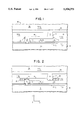
- FIG. 1 in particular there is shown a schematic drawing of a 2-D model of a multilayer circuit 10 with asymmetric trapezoidal shaped studs 12, 14 located at the ends of a metal conducting line 16.
- Stud 12 referred to as a S-type stud, connects a silicon substrate layer 18 to one end of metal conducting line 16.
- the conducting line is preferably Al/Cu, but may be any conventional conductor material used in multilayer circuit fabrication.
- a layer of quartz 20 (SiO 2 ) is deposited on the surface of silicon substrate 18.
- a layer of silicon nitride 22 (Si 3 N 4 ) is then deposited on the quartz layer 20.
- the stud 12 extends through the silicon nitrite and quartz layers to the silicon substrate.
- Stud 14 referred to as a L-type stud, connects the other end of the metal conducting line 16 to a metal conducting line 24 in the next layer.
- the metal conducting line 24 is preferably Al/Cu, but may be any conventional conductor material used in multilayer circuit fabrication.
- quartz 26 is used for passivation and embedding of the metal conducting lines and the studs.
- other passivation material such as glass, polyimide and the like can also be used.
- FIGS. 2 and 3 schematically show a modification of the multilayer circuit shown in FIG. 1.
- overhang extensions of the metal conducting lines in the length direction (x-axis) of the conducting line 16 have been added as extension 28 in the vicinity of stud 12 and as extension 30 in the vicinity of stud 14.
- FIG. 3 shows an extension 32 of the metal conducting line in the width direction (z-axis) of the conducting line in the vicinity of stud 12.
- Each stud has a contact dimension in the length direction of the conducting line 16.
- the stud 12 has a dimension at the top of stud where a joint is to be formed with the conducting line 16 in the length direction, parallel to the x-axis as shown, of L S .
- stud 14 has a dimension at the bottom of the stud where a joint is to be formed with the conducting line 16 in the length direction of L L .
- Each stud also has a contact dimension where a joint is to be formed with the conducting line 16 in the width direction of the conducting line, parallel to the z-axis as shown in FIG. 3 and in the case of the stud 12 of dimension W S .
- FIGS. 4 and 5 graphically illustrate the maximum stress components ⁇ x , ⁇ y and ⁇ xy as a function of the ratio of the length of the extension (x) of the conducting line beyond the stud and the dimension of the stud in the length dimension, L S and L L for stud 12 and stud 14 respectively.
- the values ⁇ x and ⁇ y are the stress concentration components along the x-axis and y-axis respectively.
- the value ⁇ xy is the shear stress.
- FIGS. 4 and 5 show that ⁇ y and ⁇ xy monotonically decrease as the length of the extension increases and reaches a minimum value when the length of the extension is approximately one and one-half times the stud dimension.
- the stud stiffness in the x-axis direction is much higher than the stud stiffness in the y-axis direction.
- the x-axis direction stiffness is in the range of approximately 2 to 26 times greater than the y-axis direction stiffness.
- the x-axis direction stiffness is in the range of approximately 2 to 5 times greater than the y-axis direction stiffness.
- the y-axis direction stress, ⁇ y is the more critical stress component to control than the x-axis direction stress, ⁇ x .
- Calculations and examination of failed components confirm that the prominent failure modes are related to the y-axis direction stress component ⁇ y and the shear stress ⁇ xy .
- significant stress reduction is manifest when the extension of the conducting line length is in the range of approximately one-quarter to one-half of the stud dimension for both S-type and L-type studs.
- the length of the line extension in the length direction of the line can be made up to approximately one and one-half to two times the stud dimension in order to take maximum advantage of the stress reduction afforded by practicing the present invention.
- FIG. 6 graphically illustrates the maximum stress components of the stress applied to the stud as a function of the ratio of the width of an extension (z) of the conducting line beyond a S-type stud in the direction of the line width and the stud width dimension W S .
- the stress actually increases when a short extension is added to the conducting line. Therefore, it is preferably to have no significant extension of the conducting line in the direction of the conducting line width.
- FIGS. 7a, 7b, and 7c schematically illustrate the preferred design of a S-type stud 12 and metal connecting line 16 with line extension 28 only in the direction of the line length (x-axis) and substantially without any extension in the direction of the line width (z-axis).
- FIGS. 8a, 8b and 8c schematically illustrate the preferred design of the L-type stud 14 and metal connecting line 16 with an extension 30 in the direction of the line length (x-axis) and substantially without an extension in the direction of the line width (z-axis).
Abstract
In the design of stud and conducting line joints, the conducting line is extended beyond the stud without any significant overhang of the line in the width direction for minimizing induced stress in order to reduce voids and crack growth in the region where the connecting line is joined to the stud. The preferred length of the extension is in the range approximately between one-quarter and twice the stud dimension. The design is applicable, but not limited to, multilevel integrated circuits used in computers and other electrical devices.
Description
This application is a continuation of application Ser. No. 07/844,349, filed Mar. 2, 1992 now abandoned.
The present invention relates to the design of studs and connecting line joints in multilayer electrical circuits and particularly, to the extending of the connecting line beyond an asymmetric stud in the length direction of the line without significant overhang of the line in the width direction of the line for minimizing induced stresses in order to reduce voids and crack growth in the region where the connecting line is joined to the stud.
In the manufacture of multilevel integrated circuits used in computers and other electrical devices, reliability is a constant concern. Poor reliability adversely impacts yield and results in a high incidence of field failures and product returns. Although there are a number of causes for such failures including contamination, corrosion, misalignment and so forth, experience has shown that in many instances the failure is due to the fracture of studs which connect metal conducting lines between circuit containing conductor levels of multilayer circuit structures. The fracture of the studs is a result of stress resulting from thermal mismatch between the conducting layer and the passivation layer during temperature excursion and from thermally activated voiding processes.
Thus, the reduction of the thermal stress is one of the most important factors in improving reliability. It has been discovered that most stud failures occur at the studs located in the vicinity of the end of the metal conducting line. Finite-element calculation performed by the inventors shows that the stress in the studs at the end of the metal conducting lines are approximately 20 to 40 percent higher than the stress in the studs located in the middle of the line. Therefore, reduction of the stresses in the studs at the end of the metal conducting lines is of utmost importance.
Finite-element modeling results and SEM micrographs also show that the voids formed in the studs are primarily caused by tensile normal or hydrostatic stresses. Moreover, the location for voids to grow depends on the range of the temperature excursion and the duration at a particular temperature to which the circuit is exposed. In addition to reducing stud failures by optimizing the thermal cycling of the fabrication process, which optimization tends to be process limited, the present invention provides for reduced stud failure by optimizing the design of the stud and metal conducting line joint.
It has been derived that the exact location where any voids grow is dependent upon the range of temperature excursion and the time spent at a particular temperature. It has also been discovered that enlarging the contact area of the stud does not reduce, but rather significantly increases the stresses. Furthermore, it has been found that an extension or overhang of the conducting line in the length direction of the line only, beyond the stud at the end of the line, results in a significant thermal stress reduction without causing an appreciable decrease in circuit density.
Significant stress reduction occurs in the conducting line when the overhang extension is approximately one-quarter to one-half of the stud dimension without significantly affecting the circuit density. Maximum stress reduction occurs when the line extension is up to one and one-half to two times the stud dimension.
When high circuit density is critical, for instance in memory arrays, a shorter length extension is preferred. On the other hand, when circuit density is not as critical a factor, a larger length extension is preferred.
A principal object of the present invention is therefore, the provision of a stud and connecting line joint design which minimizes stress at the joint region.
A further object of the invention is the provision of a stud and conducting line joint design where the conducting line extends beyond the stud in the length direction of the line.
Another object of the invention is the provision of a stud and conducting line joint design where the conducting line extends beyond the stud in the length direction of the line but without significant overhang in the width direction of the line.
Further and still other objects of the present invention will become more clearly apparent when the following description is read in conjunction with the accompanying drawing.
FIG. 1 is a schematic diagram of a 2-D model of a multilayer circuit with studs located at the ends of a conducting line;
FIG. 2 is a schematic diagram of a 2-D model of a multilayer circuit showing the extension of the conducting line in the length direction of the line;
FIG. 3 is a schematic diagram of a multilayer circuit showing the portion of the conducting line width beyond the stud;
FIG. 4 is a graphical representation of the stress as a function of the length of a conducting line extension beyond a S-type stud in the direction of the line length;
FIG. 5 is a graphical representation of the stress as a function of the length of a conducting line extension beyond L-type stud in the direction of the line length;
FIG. 6 is a graphical representation of the stress as a function of the length of a conducting line extension beyond the S-type stud in the direction of the line width;
FIG. 7a is a schematic diagram of a side elevation view of a S-type stud connected to a conducting line where the conducting line extends beyond the stud in the length direction of the line;
FIG. 7b is a schematic diagram of a plan view of the connection shown in FIG. 7a;
FIG. 7c is a schematic diagram of an end view of the connection shown in FIG. 7a;
FIG. 8 is a schematic diagram of a side direction view of a L-type stud connected to a conducting line when the conducting line extends beyond the stud in the length direction of the line;
FIG. 8b is a schematic diagram of a plan view of the connection shown in FIG. 8a; and
FIG. 8c is a schematic diagram of an end view of the connection shown in FIG. 8a.
While the invention is most applicable to multilayer circuits used in bi-polar chips in mainframe computers, the broad concepts and applicability of the invention applies to any electrical component where a conducting line is connected to a stud and both the connecting line and stud are contained in a passivation layer.
Referring now to the figures and to FIG. 1 in particular there is shown a schematic drawing of a 2-D model of a multilayer circuit 10 with asymmetric trapezoidal shaped studs 12, 14 located at the ends of a metal conducting line 16.
In conventional multilayer circuits, quartz 26 is used for passivation and embedding of the metal conducting lines and the studs. However, other passivation material such as glass, polyimide and the like can also be used.
FIGS. 2 and 3 schematically show a modification of the multilayer circuit shown in FIG. 1. In FIG. 2 overhang extensions of the metal conducting lines in the length direction (x-axis) of the conducting line 16 have been added as extension 28 in the vicinity of stud 12 and as extension 30 in the vicinity of stud 14. FIG. 3 shows an extension 32 of the metal conducting line in the width direction (z-axis) of the conducting line in the vicinity of stud 12.
Each stud has a contact dimension in the length direction of the conducting line 16. In FIG. 2, the stud 12 has a dimension at the top of stud where a joint is to be formed with the conducting line 16 in the length direction, parallel to the x-axis as shown, of LS. Similarly, stud 14 has a dimension at the bottom of the stud where a joint is to be formed with the conducting line 16 in the length direction of LL. Each stud also has a contact dimension where a joint is to be formed with the conducting line 16 in the width direction of the conducting line, parallel to the z-axis as shown in FIG. 3 and in the case of the stud 12 of dimension WS.
FIGS. 4 and 5 graphically illustrate the maximum stress components σx,σy and τxy as a function of the ratio of the length of the extension (x) of the conducting line beyond the stud and the dimension of the stud in the length dimension, LS and LL for stud 12 and stud 14 respectively. The values σx and σy are the stress concentration components along the x-axis and y-axis respectively. The value τxy is the shear stress.
FIGS. 4 and 5 show that σy and τxy monotonically decrease as the length of the extension increases and reaches a minimum value when the length of the extension is approximately one and one-half times the stud dimension. Based upon the stud geometry shown, the stud stiffness in the x-axis direction is much higher than the stud stiffness in the y-axis direction. In the case of S-type studs, according to calculations, the x-axis direction stiffness is in the range of approximately 2 to 26 times greater than the y-axis direction stiffness. In the case of the L-type stud, calculations show that the x-axis direction stiffness is in the range of approximately 2 to 5 times greater than the y-axis direction stiffness. Therefore, the y-axis direction stress, σy, is the more critical stress component to control than the x-axis direction stress, σx. Calculations and examination of failed components confirm that the prominent failure modes are related to the y-axis direction stress component σy and the shear stress τxy. It should also be noted from FIGS. 4 and 5 that significant stress reduction is manifest when the extension of the conducting line length is in the range of approximately one-quarter to one-half of the stud dimension for both S-type and L-type studs. Thus, even a relatively short extension of the conducting line in the length direction of the line can provide a significant improvement in reliability with only a minimal impact or decrease in circuit density. This result is particularly significant in the manufacture of memory arrays. However, when designing multilayer circuits where circuit density is a less important consideration, the length of the line extension in the length direction of the line can be made up to approximately one and one-half to two times the stud dimension in order to take maximum advantage of the stress reduction afforded by practicing the present invention.
FIG. 6 graphically illustrates the maximum stress components of the stress applied to the stud as a function of the ratio of the width of an extension (z) of the conducting line beyond a S-type stud in the direction of the line width and the stud width dimension WS. The stress actually increases when a short extension is added to the conducting line. Therefore, it is preferably to have no significant extension of the conducting line in the direction of the conducting line width.
FIGS. 7a, 7b, and 7c schematically illustrate the preferred design of a S-type stud 12 and metal connecting line 16 with line extension 28 only in the direction of the line length (x-axis) and substantially without any extension in the direction of the line width (z-axis). Similarly, FIGS. 8a, 8b and 8c schematically illustrate the preferred design of the L-type stud 14 and metal connecting line 16 with an extension 30 in the direction of the line length (x-axis) and substantially without an extension in the direction of the line width (z-axis).
While there has been described and illustrated a preferred embodiment of the present invention, it will be apparent to those skilled in the art that variations and modifications are possible without deviating from the broad scope of the present invention which shall be limited solely by the scope of the claims appended hereto.
Claims (8)
1. An interconnection structure for reducing thermal stress in a multilayer circuit comprising:
a first electrically conductive stud having a first contact area;
a second electrically conductive stud
having a second contact area;
a conducting line extending lengthwise along a first axis, said conducting line forming at a first end thereof a first joint with the first contact area of said first stud and forming at a second end thereof a second joint with the second contact area of said second stud;
passivation layer means disposed for embedding said first stud and said first joint, said second stud and said second joint, and said conducting line, said first and second studs being disposed in corresponding first and second vias in said passivation layer means;
the first end of said conducting line extending a first predetermined distance beyond said first contact area along said first axis, and the second end of said conducting line extending a second predetermined distance beyond said second contact area along said first axis, said first and second predetermined distances being chosen so as to reduce thermal stress at said first and second joints, respectively, while accommodating desired circuit density;
said first contact area having a first length dimension along said first axis, said second contact area having a second length dimension along said first axis, and said first predetermined distance being in the range of one-quarter to twice the first length dimension, and said second predetermined distance being in the range of one-quarter to twice the second length dimension; and
said first contact area has a first width dimension along a second axis orthogonal to said first axis, said second contact area has a second width dimension along said second axis, and said conducting line has a width at said first joint substantially equal to said first width dimension and a width at said second joint substantially equal to said second width dimension.
2. The interconnection structure of claim 1 wherein said first predetermined distance is chosen to be in the range of one-quarter to one-half the first length dimension and said second predetermined distance is chosen to be in the range of one-quarter to one-half the second length dimension in order to accommodate high circuit density.
3. The interconnection structure of claim 1 wherein said first predetermined distance is chosen to be in the range of one and one-half to twice the first length dimension, and the second predetermined distance is chosen to be in the range of one and one-half to twice the second length dimension in order to maximize stress reduction at the first and second joints, respectively.
4. The multilayer circuit interconnection structure of claim 1 wherein said first stud comprises an S-type stud.
5. The multilayer circuit interconnection structure of claim 4 wherein said second stud comprises an L-type stud.
6. In an electrical component in which an end of a conducting line is connected to a contact area of a stud, the conducting line extending lengthwise along a first axis, and both the conducting line and stud are contained in a passivation layer, the improvement comprising:
an overhang of the connecting line end extending along the first axis a predetermined distance beyond the contact area, said predetermined distance being chosen so as to reduce thermal stress at the contact area while accommodating desired circuit density, said predetermined distance being in the range of one-quarter to twice a length dimension of said contact area, said length dimension being measured along said first axis; and wherein said conducting line end does not overhang said contact area in a width direction orthogonal to said first axis, whereby thermal stress at said contact area is reduced.
7. The improved electrical component of claim 6 wherein said predetermined distance is chosen to be in the range of one-quarter to one-half said length dimension in order to accommodate high circuit density.
8. The improved electrical component of claim 6 wherein said predetermined distance is chosen to be in the range of one and one-half to two times said length dimension in order to maximize stress reduction.
Priority Applications (1)
| Application Number | Priority Date | Filing Date | Title |
|---|---|---|---|
| US08/155,492 US5504375A (en) | 1992-03-02 | 1993-11-18 | Asymmetric studs and connecting lines to minimize stress |
Applications Claiming Priority (2)
| Application Number | Priority Date | Filing Date | Title |
|---|---|---|---|
| US84434992A | 1992-03-02 | 1992-03-02 | |
| US08/155,492 US5504375A (en) | 1992-03-02 | 1993-11-18 | Asymmetric studs and connecting lines to minimize stress |
Related Parent Applications (1)
| Application Number | Title | Priority Date | Filing Date |
|---|---|---|---|
| US84434992A Continuation | 1992-03-02 | 1992-03-02 |
Publications (1)
| Publication Number | Publication Date |
|---|---|
| US5504375A true US5504375A (en) | 1996-04-02 |
Family
ID=25292476
Family Applications (1)
| Application Number | Title | Priority Date | Filing Date |
|---|---|---|---|
| US08/155,492 Expired - Fee Related US5504375A (en) | 1992-03-02 | 1993-11-18 | Asymmetric studs and connecting lines to minimize stress |
Country Status (1)
| Country | Link |
|---|---|
| US (1) | US5504375A (en) |
Cited By (5)
| Publication number | Priority date | Publication date | Assignee | Title |
|---|---|---|---|---|
| US5747857A (en) * | 1991-03-13 | 1998-05-05 | Matsushita Electric Industrial Co., Ltd. | Electronic components having high-frequency elements and methods of manufacture therefor |
| US5905307A (en) * | 1995-05-01 | 1999-05-18 | Oki Electric Industry Co., Ltd. | Semiconductor device incorporating multilayer wiring structure |
| WO2002056364A2 (en) * | 2001-01-11 | 2002-07-18 | Advanced Micro Devices, Inc. | Conductor reservoir volume for integrated circuit interconnects |
| WO2003049178A2 (en) * | 2001-11-30 | 2003-06-12 | Motorola, Inc. | Semiconductor power device metal structure and method of formation |
| CN116525766A (en) * | 2023-06-27 | 2023-08-01 | 宁德时代新能源科技股份有限公司 | Secondary battery and electricity utilization device |
Citations (11)
| Publication number | Priority date | Publication date | Assignee | Title |
|---|---|---|---|---|
| US3874072A (en) * | 1972-03-27 | 1975-04-01 | Signetics Corp | Semiconductor structure with bumps and method for making the same |
| US4582563A (en) * | 1983-11-28 | 1986-04-15 | Kabushiki Kaisha Toshiba | Process for forming multi-layer interconnections |
| US4614021A (en) * | 1985-03-29 | 1986-09-30 | Motorola, Inc. | Pillar via process |
| JPS61287138A (en) * | 1985-06-13 | 1986-12-17 | Matsushita Electric Ind Co Ltd | Semiconductor device |
| US4905068A (en) * | 1987-03-10 | 1990-02-27 | Mitsubishi Denki Kabushiki Kaisha | Semiconductor device having interconnection layers of T-shape cross section |
| US4908690A (en) * | 1986-10-29 | 1990-03-13 | Mitsubishi Denki Kabushiki Kaisha | Semiconductor integrated circuit device with high reliability wiring layers |
| US4914056A (en) * | 1985-05-13 | 1990-04-03 | Kabushiki Kaisha Toshiba | Method of manufacturing a semiconductor device having tapered pillars |
| US4960489A (en) * | 1988-12-16 | 1990-10-02 | Siemens Aktiengesellschaft | Method for self-aligned manufacture of contacts between interconnects contained in wiring levels arranged above one another in an integrated circuit |
| US5025303A (en) * | 1988-02-26 | 1991-06-18 | Texas Instruments Incorporated | Product of pillar alignment and formation process |
| US5034799A (en) * | 1989-02-22 | 1991-07-23 | Kabushiki Kaisha Toshiba | Semiconductor integrated circuit device having a hollow multi-layered lead structure |
| US5063175A (en) * | 1986-09-30 | 1991-11-05 | North American Philips Corp., Signetics Division | Method for manufacturing a planar electrical interconnection utilizing isotropic deposition of conductive material |
-
1993
- 1993-11-18 US US08/155,492 patent/US5504375A/en not_active Expired - Fee Related
Patent Citations (11)
| Publication number | Priority date | Publication date | Assignee | Title |
|---|---|---|---|---|
| US3874072A (en) * | 1972-03-27 | 1975-04-01 | Signetics Corp | Semiconductor structure with bumps and method for making the same |
| US4582563A (en) * | 1983-11-28 | 1986-04-15 | Kabushiki Kaisha Toshiba | Process for forming multi-layer interconnections |
| US4614021A (en) * | 1985-03-29 | 1986-09-30 | Motorola, Inc. | Pillar via process |
| US4914056A (en) * | 1985-05-13 | 1990-04-03 | Kabushiki Kaisha Toshiba | Method of manufacturing a semiconductor device having tapered pillars |
| JPS61287138A (en) * | 1985-06-13 | 1986-12-17 | Matsushita Electric Ind Co Ltd | Semiconductor device |
| US5063175A (en) * | 1986-09-30 | 1991-11-05 | North American Philips Corp., Signetics Division | Method for manufacturing a planar electrical interconnection utilizing isotropic deposition of conductive material |
| US4908690A (en) * | 1986-10-29 | 1990-03-13 | Mitsubishi Denki Kabushiki Kaisha | Semiconductor integrated circuit device with high reliability wiring layers |
| US4905068A (en) * | 1987-03-10 | 1990-02-27 | Mitsubishi Denki Kabushiki Kaisha | Semiconductor device having interconnection layers of T-shape cross section |
| US5025303A (en) * | 1988-02-26 | 1991-06-18 | Texas Instruments Incorporated | Product of pillar alignment and formation process |
| US4960489A (en) * | 1988-12-16 | 1990-10-02 | Siemens Aktiengesellschaft | Method for self-aligned manufacture of contacts between interconnects contained in wiring levels arranged above one another in an integrated circuit |
| US5034799A (en) * | 1989-02-22 | 1991-07-23 | Kabushiki Kaisha Toshiba | Semiconductor integrated circuit device having a hollow multi-layered lead structure |
Non-Patent Citations (14)
| Title |
|---|
| C. Y. Li et al "Analysis of thermal stress-induced grain boundary cavitation and notching in narrow Al-Si metallization", Appl. Phys. Lett. 53(1) 31 (1988). |
| C. Y. Li et al Analysis of thermal stress induced grain boundary cavitation and notching in narrow Al Si metallization , Appl. Phys. Lett. 53(1) 31 (1988). * |
| J. W. McPherson et al "A model for stress-induced metal notching and voiding in very large-scale-integrated Al-Si (1%) metallization", J. Vac. Sci. Technol. B5(5), 1321 (1987). |
| J. W. McPherson et al A model for stress induced metal notching and voiding in very large scale integrated Al Si (1%) metallization , J. Vac. Sci. Technol. B5(5), 1321 (1987). * |
| K. Hinode et al, "Stree-Induced grain boundary fractures in Al-Si interconnects", J. Vac. Sci. Technol. B5(2), 518 (1987). |
| K. Hinode et al, Stree Induced grain boundary fractures in Al Si interconnects , J. Vac. Sci. Technol. B5(2), 518 (1987). * |
| P. A. Flinn et al, "Measurement and Interpretation of Stress in Aluminum-Based Metalliztaion as a Function of Thermal History", IEEE Trans. on Electron Devices, vol. ED-34, No. 3, 689 (1987). |
| P. A. Flinn et al, Measurement and Interpretation of Stress in Aluminum Based Metalliztaion as a Function of Thermal History , IEEE Trans. on Electron Devices, vol. ED 34, No. 3, 689 (1987). * |
| Q. Guo, et al "A stress induced diffusion model for failure of interconnects in microelectronic devices", Northwest University Research Report (1990). |
| Q. Guo, et al A stress induced diffusion model for failure of interconnects in microelectronic devices , Northwest University Research Report (1990). * |
| S. Mayumi, et al, "The Effect of Cu Addition to Al-Si Interconnects on Stress Induced Open-Circuit Failures", 1987 IEEE/IRPS, pp. 15-21. |
| S. Mayumi, et al, The Effect of Cu Addition to Al Si Interconnects on Stress Induced Open Circuit Failures , 1987 IEEE/IRPS, pp. 15 21. * |
| T. Sullivan "Thermal dependence of voiding in narrow aluminum microelectronic interconnects", Appl. Phys. Lett. 55(23) 2399 (1989). |
| T. Sullivan Thermal dependence of voiding in narrow aluminum microelectronic interconnects , Appl. Phys. Lett. 55(23) 2399 (1989). * |
Cited By (13)
| Publication number | Priority date | Publication date | Assignee | Title |
|---|---|---|---|---|
| US5747857A (en) * | 1991-03-13 | 1998-05-05 | Matsushita Electric Industrial Co., Ltd. | Electronic components having high-frequency elements and methods of manufacture therefor |
| US5905307A (en) * | 1995-05-01 | 1999-05-18 | Oki Electric Industry Co., Ltd. | Semiconductor device incorporating multilayer wiring structure |
| WO2002056364A2 (en) * | 2001-01-11 | 2002-07-18 | Advanced Micro Devices, Inc. | Conductor reservoir volume for integrated circuit interconnects |
| US20020195714A1 (en) * | 2001-01-11 | 2002-12-26 | Marathe Amit P. | Method for forming conductor reservoir volume for integrated circuit interconnects |
| WO2002056364A3 (en) * | 2001-01-11 | 2003-01-23 | Advanced Micro Devices Inc | Conductor reservoir volume for integrated circuit interconnects |
| US6939803B2 (en) | 2001-01-11 | 2005-09-06 | Advanced Micro Devices, Inc. | Method for forming conductor reservoir volume for integrated circuit interconnects |
| WO2003049178A3 (en) * | 2001-11-30 | 2004-05-27 | Motorola Inc | Semiconductor power device metal structure and method of formation |
| US6888246B2 (en) | 2001-11-30 | 2005-05-03 | Freescale Semiconductor, Inc. | Semiconductor power device with shear stress compensation |
| WO2003049178A2 (en) * | 2001-11-30 | 2003-06-12 | Motorola, Inc. | Semiconductor power device metal structure and method of formation |
| CN1326221C (en) * | 2001-11-30 | 2007-07-11 | 自由度半导体公司 | Semiconductor power device and forming method |
| KR100922704B1 (en) * | 2001-11-30 | 2009-10-22 | 프리스케일 세미컨덕터, 인크. | Semiconductor power device |
| CN116525766A (en) * | 2023-06-27 | 2023-08-01 | 宁德时代新能源科技股份有限公司 | Secondary battery and electricity utilization device |
| CN116525766B (en) * | 2023-06-27 | 2023-09-26 | 宁德时代新能源科技股份有限公司 | Secondary battery and electricity utilization device |
Similar Documents
| Publication | Publication Date | Title |
|---|---|---|
| US5900675A (en) | Organic controlled collapse chip connector (C4) ball grid array (BGA) chip carrier with dual thermal expansion rates | |
| US6635960B2 (en) | Angled edge connections for multichip structures | |
| US7595222B2 (en) | Semiconductor device and manufacturing method thereof | |
| US4754371A (en) | Large scale integrated circuit package | |
| JP3210547B2 (en) | Electroplating solder terminal and method of manufacturing the same | |
| US9543261B2 (en) | Designs and methods for conductive bumps | |
| US7741207B2 (en) | Semiconductor device with multilayered metal pattern | |
| US20150011086A1 (en) | Novel conductor layout technique to reduce stress-induced void formations | |
| US4970570A (en) | Use of tapered head pin design to improve the stress distribution in the braze joint | |
| US7294909B2 (en) | Electronic package repair process | |
| EP0908951B1 (en) | Improved air isolated crossovers | |
| US6756666B2 (en) | Surface mount package including terminal on its side | |
| US20080029888A1 (en) | Solder Interconnect Joints For A Semiconductor Package | |
| US5504375A (en) | Asymmetric studs and connecting lines to minimize stress | |
| US6829149B1 (en) | Placement of sacrificial solder balls underneath the PBGA substrate | |
| EP0581712A2 (en) | MLC conductor pattern off-set design to eliminate line to via cracking | |
| JP3221383B2 (en) | Multilayer wiring structure of semiconductor device | |
| US20080157359A1 (en) | Crack-resistant solder joint, electronic component such as circuit substrate having the solder joint, semiconductor device, and manufacturing method of electronic component | |
| US20050263883A1 (en) | Asymmetric bump structure | |
| US6255599B1 (en) | Relocating the neutral plane in a PBGA substrate to eliminate chip crack and interfacial delamination | |
| JPH07118340B2 (en) | Connector assembly | |
| US7129581B2 (en) | Semiconductor device, method of manufacturing thereof, circuit board and electronic apparatus | |
| JPH0582937A (en) | Semiconductor device | |
| JPH0219978B2 (en) | ||
| JPS63278343A (en) | Solid state electronic device |
Legal Events
| Date | Code | Title | Description |
|---|---|---|---|
| FEPP | Fee payment procedure |
Free format text: PAYOR NUMBER ASSIGNED (ORIGINAL EVENT CODE: ASPN); ENTITY STATUS OF PATENT OWNER: LARGE ENTITY |
|
| FPAY | Fee payment |
Year of fee payment: 4 |
|
| REMI | Maintenance fee reminder mailed | ||
| LAPS | Lapse for failure to pay maintenance fees | ||
| FP | Lapsed due to failure to pay maintenance fee |
Effective date: 20040402 |
|
| STCH | Information on status: patent discontinuation |
Free format text: PATENT EXPIRED DUE TO NONPAYMENT OF MAINTENANCE FEES UNDER 37 CFR 1.362 |