US5506756A - Tape BGA package die-up/die down - Google Patents
Tape BGA package die-up/die down Download PDFInfo
- Publication number
- US5506756A US5506756A US08/391,253 US39125395A US5506756A US 5506756 A US5506756 A US 5506756A US 39125395 A US39125395 A US 39125395A US 5506756 A US5506756 A US 5506756A
- Authority
- US
- United States
- Prior art keywords
- die
- circuit board
- integrated circuit
- package
- solder
- Prior art date
- Legal status (The legal status is an assumption and is not a legal conclusion. Google has not performed a legal analysis and makes no representation as to the accuracy of the status listed.)
- Expired - Lifetime
Links
Images


Classifications
-
- H—ELECTRICITY
- H01—ELECTRIC ELEMENTS
- H01L—SEMICONDUCTOR DEVICES NOT COVERED BY CLASS H10
- H01L23/00—Details of semiconductor or other solid state devices
- H01L23/28—Encapsulations, e.g. encapsulating layers, coatings, e.g. for protection
- H01L23/31—Encapsulations, e.g. encapsulating layers, coatings, e.g. for protection characterised by the arrangement or shape
- H01L23/3107—Encapsulations, e.g. encapsulating layers, coatings, e.g. for protection characterised by the arrangement or shape the device being completely enclosed
- H01L23/3121—Encapsulations, e.g. encapsulating layers, coatings, e.g. for protection characterised by the arrangement or shape the device being completely enclosed a substrate forming part of the encapsulation
- H01L23/3128—Encapsulations, e.g. encapsulating layers, coatings, e.g. for protection characterised by the arrangement or shape the device being completely enclosed a substrate forming part of the encapsulation the substrate having spherical bumps for external connection
-
- H—ELECTRICITY
- H01—ELECTRIC ELEMENTS
- H01L—SEMICONDUCTOR DEVICES NOT COVERED BY CLASS H10
- H01L23/00—Details of semiconductor or other solid state devices
- H01L23/48—Arrangements for conducting electric current to or from the solid state body in operation, e.g. leads, terminal arrangements ; Selection of materials therefor
- H01L23/488—Arrangements for conducting electric current to or from the solid state body in operation, e.g. leads, terminal arrangements ; Selection of materials therefor consisting of soldered or bonded constructions
- H01L23/498—Leads, i.e. metallisations or lead-frames on insulating substrates, e.g. chip carriers
- H01L23/49811—Additional leads joined to the metallisation on the insulating substrate, e.g. pins, bumps, wires, flat leads
- H01L23/49816—Spherical bumps on the substrate for external connection, e.g. ball grid arrays [BGA]
-
- H—ELECTRICITY
- H01—ELECTRIC ELEMENTS
- H01L—SEMICONDUCTOR DEVICES NOT COVERED BY CLASS H10
- H01L2224/00—Indexing scheme for arrangements for connecting or disconnecting semiconductor or solid-state bodies and methods related thereto as covered by H01L24/00
- H01L2224/01—Means for bonding being attached to, or being formed on, the surface to be connected, e.g. chip-to-package, die-attach, "first-level" interconnects; Manufacturing methods related thereto
- H01L2224/42—Wire connectors; Manufacturing methods related thereto
- H01L2224/47—Structure, shape, material or disposition of the wire connectors after the connecting process
- H01L2224/48—Structure, shape, material or disposition of the wire connectors after the connecting process of an individual wire connector
- H01L2224/481—Disposition
- H01L2224/48151—Connecting between a semiconductor or solid-state body and an item not being a semiconductor or solid-state body, e.g. chip-to-substrate, chip-to-passive
- H01L2224/48221—Connecting between a semiconductor or solid-state body and an item not being a semiconductor or solid-state body, e.g. chip-to-substrate, chip-to-passive the body and the item being stacked
- H01L2224/48225—Connecting between a semiconductor or solid-state body and an item not being a semiconductor or solid-state body, e.g. chip-to-substrate, chip-to-passive the body and the item being stacked the item being non-metallic, e.g. insulating substrate with or without metallisation
- H01L2224/48227—Connecting between a semiconductor or solid-state body and an item not being a semiconductor or solid-state body, e.g. chip-to-substrate, chip-to-passive the body and the item being stacked the item being non-metallic, e.g. insulating substrate with or without metallisation connecting the wire to a bond pad of the item
-
- H—ELECTRICITY
- H01—ELECTRIC ELEMENTS
- H01L—SEMICONDUCTOR DEVICES NOT COVERED BY CLASS H10
- H01L2224/00—Indexing scheme for arrangements for connecting or disconnecting semiconductor or solid-state bodies and methods related thereto as covered by H01L24/00
- H01L2224/73—Means for bonding being of different types provided for in two or more of groups H01L2224/10, H01L2224/18, H01L2224/26, H01L2224/34, H01L2224/42, H01L2224/50, H01L2224/63, H01L2224/71
- H01L2224/732—Location after the connecting process
- H01L2224/73251—Location after the connecting process on different surfaces
- H01L2224/73257—Bump and wire connectors
-
- H—ELECTRICITY
- H01—ELECTRIC ELEMENTS
- H01L—SEMICONDUCTOR DEVICES NOT COVERED BY CLASS H10
- H01L2924/00—Indexing scheme for arrangements or methods for connecting or disconnecting semiconductor or solid-state bodies as covered by H01L24/00
- H01L2924/15—Details of package parts other than the semiconductor or other solid state devices to be connected
- H01L2924/151—Die mounting substrate
- H01L2924/1515—Shape
- H01L2924/15151—Shape the die mounting substrate comprising an aperture, e.g. for underfilling, outgassing, window type wire connections
-
- H—ELECTRICITY
- H01—ELECTRIC ELEMENTS
- H01L—SEMICONDUCTOR DEVICES NOT COVERED BY CLASS H10
- H01L2924/00—Indexing scheme for arrangements or methods for connecting or disconnecting semiconductor or solid-state bodies as covered by H01L24/00
- H01L2924/15—Details of package parts other than the semiconductor or other solid state devices to be connected
- H01L2924/151—Die mounting substrate
- H01L2924/153—Connection portion
- H01L2924/1531—Connection portion the connection portion being formed only on the surface of the substrate opposite to the die mounting surface
- H01L2924/15311—Connection portion the connection portion being formed only on the surface of the substrate opposite to the die mounting surface being a ball array, e.g. BGA
-
- H—ELECTRICITY
- H01—ELECTRIC ELEMENTS
- H01L—SEMICONDUCTOR DEVICES NOT COVERED BY CLASS H10
- H01L2924/00—Indexing scheme for arrangements or methods for connecting or disconnecting semiconductor or solid-state bodies as covered by H01L24/00
- H01L2924/15—Details of package parts other than the semiconductor or other solid state devices to be connected
- H01L2924/181—Encapsulation
- H01L2924/1815—Shape
- H01L2924/1816—Exposing the passive side of the semiconductor or solid-state body
- H01L2924/18165—Exposing the passive side of the semiconductor or solid-state body of a wire bonded chip
Landscapes
- Engineering & Computer Science (AREA)
- Microelectronics & Electronic Packaging (AREA)
- Physics & Mathematics (AREA)
- Condensed Matter Physics & Semiconductors (AREA)
- General Physics & Mathematics (AREA)
- Computer Hardware Design (AREA)
- Power Engineering (AREA)
- Cooling Or The Like Of Semiconductors Or Solid State Devices (AREA)
Abstract
A ball grid array (BGA) package which contains an integrated circuit die that is directly mounted to either a heat sink or a printed circuit board. In one embodiment, the package has an integrated circuit with surface pads that are coupled to a flexible circuit board. Solder balls are attached to the flexible circuit board and solder the BGA package to a printed circuit board. The flexible circuit has an opening that exposes the integrated circuit and allows the IC to be soldered to the printed circuit board by solder balls attached directly to the surface pads of the IC die. The direct attachment between the die and printed circuit board increases the number of IC output pins. The flexible circuit board and die are covered by a protective injection molded plastic housing. In a second embodiment, the integrated circuit die is flipped upside down and a surface of the die is exposed through the plastic housing. A heat sink can be attached to the exposed die surface to improve the thermal performance of the package.
Description
This is a continuation of patent application Ser. No. 08/187,627 filed Jan. 25 1994, now abandoned.
1. Field of the Invention
The present invention relates to a package for an integrated circuit.
2. Description of Related Art
Integrated circuits are typically housed within a package that is mounted to a printed circuit board. The package has conductive leads or pins that are soldered to the printed circuit board and coupled to the integrated circuit by a lead frame. One type of conventional IC package is a quad flat pack (QFP), which has a plurality of gull wing shaped leads that extend from each side of the package housing. The outward extension of the gull wing leads, allows the leads to be readily soldered and inspected after assembly to the printed circuit board. The gull wing shape of the leads also compensates for any deviation in flatness between the printed circuit board and the package.
Another common type of package is a pin grid array (PGA) which has a matrix of output pins across the bottom surface of the package. The pin grid array increases the I/O of the package. PGA packages are difficult to inspect and may result in poor solder joints, if there is a discrepancy in the length of the pins and/or the flatness in the package or printed circuit board.
U.S. Pat. Nos. 5,045,921 and 5,216,278 issued to Lin et al., disclose an integrated circuit package which has a plurality of solder balls that interconnect the package to a printed circuit board. The Lin package is commonly referred to as a ball grid array (BGA). The solder balls are attached to a polyimide based flexible circuit board which has a number of conductive traces and accompanying solder pads. The IC die is connected to the solder pads of the flexible circuit by wire bonds, and electrically coupled to the solder balls through conductive traces routed across the flexible circuit. Vias are formed in the polyimide to interconnect each side of the flexible circuit.
The integrated circuit die of the Lin packages are mounted to a substrate and enclosed by a rigid housing or lid, typically constructed from a molded plastic material. The solder balls are relatively flexible and can thus compensate for any lack of flatness in the printed circuit board or package. Additionally, the solder balls are assembled in a an array on the bottom of the package, and thus provide a relatively high throughput.
Newly developed integrated circuits are continually designed with larger I/O and power requirements than existing ICs. These requirements necessitate packages that are more thermally efficient and have a larger number of output pins. It would be desirable to have BGA packages which are thermally efficient and provide more I/O, than packages in the prior art.
The present invention is a ball grid array (BGA) package which contains an integrated circuit die that is directly mounted to either a heat sink or a printed circuit board. In one embodiment, the package has an integrated circuit with surface pads that are coupled to a flexible circuit board. Solder balls are attached to the flexible circuit board and the integrated circuit. The center balls solder the BGA package to a printed circuit board. The flexible circuit has an opening that exposes the integrated circuit and allows the IC to be soldered to the printed circuit board by solder balls attached directly to the surface pads of the IC die. The direct attachment between the die and printed circuit board increases the number of IC output pins. The flexible circuit board and die are covered by a protective injection molded plastic housing. In a second embodiment, the integrated circuit die is flipped upside down and a surface of the die is exposed through the plastic housing. A heat sink can be attached to the exposed die surface to improve the thermal performance of the package.
The objects and advantages of the present invention will become more readily apparent to those ordinarily skilled in the art after reviewing the following detailed description and accompanying drawings, wherein:
FIG. 1 is a cross-sectional view of an integrated circuit package of the present invention;
FIG. 2 is a top view of a flexible circuit board of the package;
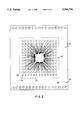
FIG. 3 is a bottom view of the package of FIG. 1;
FIG. 4 is a perspective view showing the package being assembled;
FIG. 5 is cross-sectional view showing an alternate embodiment of the package of FIG. 1;
FIG. 6 is a bottom view an alternate embodiment of the package in FIG. 5.
Referring to the drawings more particularly by reference numbers, FIG. 1 shows an integrated circuit package 10 of the present invention. The package 10 contains an integrated circuit die 12 within a housing 14. The integrated circuit 12 may be a microprocessor, a memory device, etc. The housing is constructed from a plastic material preferably injection molded into the configuration shown. The package 10 is typically mounted to a printed circuit board (not shown) which can couple the integrated circuit to other electrical components, as is known in the art.
The package 10 has a flexible circuit board 16 that is coupled to the integrated circuit 12 by bonded wires 18. As shown in FIG. 2, the circuit board 16 is typically constructed and cut from a flexible polyimide tape material 20. The flexible circuit board 16 has a plurality of conductive lines 22 on a first surface 24 of the tape 20. The lines 22 terminate at Vias 26 which extend through the tape 20 to surface pads 28 located on the second surface 30 of the flexible circuit board 16.
As shown in FIG. 3, attached to each surface pad 28 is a solder ball 32. The solder balls 32 are typically soldered to the surface pads of a printed circuit board (not shown), by mounting the package 10 to the circuit board and reflowing the solder. The solder balls 32 are preferably constructed from a relatively resilient material such as a 60:40 lead-tin composition, 62:36:2 lead-tin-silver composition or an indium alloy. The resilient nature of the solder balls 32 allows the solder joints to withstand the stresses created within the joints. Stresses are created when the package and printed circuit board have different coefficients of thermal expansion and the overall assembly is exposed to varying temperatures. The thermal cycling of the assembly causes the printed circuit board and package to expand and contract at different rates, thereby creating stress in the solder joint.
As shown in FIG. 1, the wires 18 are bonded to the traces 22 of the tape 16 and first surface output pads 34 located on a first surface 36 of the IC die 12. Alternatively the surface pads 34 of the die 12 can be coupled to the tape 16 by conventional TAB (tape automated bonding) tape. The die 12 also has a plurality of second surface output pads 38 located on a second opposite surface 40 of the integrated circuit 12. As shown in FIG. 3, the flexible circuit board 16 has an opening 42 that exposes the second surface 40 of the die 12. The opening 42 allows solder balls 32 to be attached to the second surface pads 38 of the integrated circuit 12. The solder balls 32 located on the die 12 directly couple the integrated circuit 12 to the printed circuit board (not shown) and increase the I/O of the IC. A solder mask 44 preferably covers the portion of the second surface 40 around the solder balls 32. The solder mask 44 environmentally protects the integrated circuit, strengthens the solder joints, and prevents solder from cross-flowing and creating a short circuit between solder joints.
The solder balls 32 and second surface output pads 38 not only increase the number of pins of the package 10, but also increase the number of output pins on the integrated circuit itself. The additional pins can be dedicated to ground or power thereby increasing the number of data signals that can be routed to the IC through the top surface pads 34 of the die 12.
FIG. 4 shows a method for assembling the package 10. The integrated circuit 12 is first wire bonded to the flexible circuit board 16. The die 12 and flexible circuit 16 are then placed in a mold 48, such that the flexible circuit 16 and second surface 40 of the integrated circuit 12 are lying on the surface of the mold 48. The mold 48 is then filled with a plastic material, which cures and forms the housing 14. The solder mask 44 is applied to the second surface 40 of the die in a manner that only exposes the second surface pads 38. The solder balls 34 are then attached to the second solder pads 28 of the flexible circuit 16 and the second surface pads 38 of the integrated circuit 12. The flexible circuit board 16 is then trimmed to the edge of the housing 14 to finish the package 10. The cured housing material 14 provides enough stiffness to structurally support the integrated circuit 12, there is no need to mount the die 12 to a substrate as required in packages in the prior art.
FIGS. 5 and 6 show an alternate embodiment of the package, wherein the integrated circuit 12 is rotated so that the first die surface 36 is facing in the same direction as the solder balls 32. The second die surface 40 is exposed through the top surface 50 of the housing 14. The exposed second surface 40 can be readily cooled through either natural or forced convection means. A heat sink 52 can be mounted directly to the second surface 40 to increase the thermal performance of the package.
The package shown in FIGS. 5 and 6 can be constructed similar to the package shown in FIG. 4. The second die surface 40 is placed onto the mold 48. The mold 48 has a feature that would support the flexible circuit 16 above the die 12. The mold 48 is filled with a plastic material, which cures to form the housing 14. A solder mask 44 may be applied to the die 12 to cover the second surface 40. The solder mask 44 can also be applied to the second surface of the flexible circuit board 16 to protect the surface pads 28 and solder balls 32.
What is thus provided are BGA packages that are more thermally efficient and have a greater throughput than BGA packages in the prior art.
While certain exemplary embodiments have been described and shown in the accompanying drawings, it is to be understood that such embodiments are merely illustrative of and not restrictive on the broad invention, and that this invention not be limited to the specific constructions and arrangements shown and described, since various other modifications may occur to those ordinarily skilled in the art.
Claims (4)
1. An electronic package, comprising:
an integrated circuit which has a first surface that has a plurality of first surface pads and an opposite second surface that has a plurality of second surface pads;
a housing which extends around said integrated circuit such that said second surface of said integrated circuit is exposed, said housing having a first surface and an opposite second surface that is essentially coplanar with said exposed second surface of said integrated circuit;
a tape attached to said second surface of said housing, said tape having a plurality of conductive traces that are coupled to said first surface pads of said integrated circuit, said tape further having an opening that exposes said second surface of said integrated circuit; and,
a plurality of solder balls coupled to said conductive traces of said tape and said second surface pads of said exposed second surface of said integrated circuit.
2. The electronic package as recited in claim 1, wherein said housing is constructed from a molded plastic material.
3. The electronic package as recited in claim 1, further comprising a solder mask on said second surface of said integrated circuit.
4. The electronic package as recited in claim 1, further comprising a plurality of wires that couple said integrated circuit to said conductive traces of said tape.
Priority Applications (1)
| Application Number | Priority Date | Filing Date | Title |
|---|---|---|---|
| US08/391,253 US5506756A (en) | 1994-01-25 | 1995-02-17 | Tape BGA package die-up/die down |
Applications Claiming Priority (2)
| Application Number | Priority Date | Filing Date | Title |
|---|---|---|---|
| US18762794A | 1994-01-25 | 1994-01-25 | |
| US08/391,253 US5506756A (en) | 1994-01-25 | 1995-02-17 | Tape BGA package die-up/die down |
Related Parent Applications (1)
| Application Number | Title | Priority Date | Filing Date |
|---|---|---|---|
| US18762794A Continuation | 1994-01-25 | 1994-01-25 |
Publications (1)
| Publication Number | Publication Date |
|---|---|
| US5506756A true US5506756A (en) | 1996-04-09 |
Family
ID=22689769
Family Applications (1)
| Application Number | Title | Priority Date | Filing Date |
|---|---|---|---|
| US08/391,253 Expired - Lifetime US5506756A (en) | 1994-01-25 | 1995-02-17 | Tape BGA package die-up/die down |
Country Status (1)
| Country | Link |
|---|---|
| US (1) | US5506756A (en) |
Cited By (47)
| Publication number | Priority date | Publication date | Assignee | Title |
|---|---|---|---|---|
| WO1997037383A1 (en) * | 1996-04-02 | 1997-10-09 | Micron Technology, Inc. | Standardized bonding location process and apparatus |
| US5729051A (en) * | 1994-09-22 | 1998-03-17 | Nec Corporation | Tape automated bonding type semiconductor device |
| US5736780A (en) * | 1995-11-07 | 1998-04-07 | Shinko Electric Industries Co., Ltd. | Semiconductor device having circuit pattern along outer periphery of sealing resin and related processes |
| US5768774A (en) * | 1995-06-07 | 1998-06-23 | International Business Machines | Thermally enhanced ball grid array package |
| US5835355A (en) * | 1997-09-22 | 1998-11-10 | Lsi Logic Corporation | Tape ball grid array package with perforated metal stiffener |
| US5841198A (en) * | 1997-04-21 | 1998-11-24 | Lsi Logic Corporation | Ball grid array package employing solid core solder balls |
| US5874784A (en) * | 1995-10-25 | 1999-02-23 | Sharp Kabushiki Kaisha | Semiconductor device having external connection terminals provided on an interconnection plate and fabrication process therefor |
| US5892290A (en) * | 1995-10-28 | 1999-04-06 | Institute Of Microelectronics | Highly reliable and planar ball grid array package |
| US5894166A (en) * | 1997-09-17 | 1999-04-13 | Northern Telecom Limited | Chip mounting scheme |
| US5900312A (en) * | 1996-11-08 | 1999-05-04 | W. L. Gore & Associates, Inc. | Integrated circuit chip package assembly |
| US5923959A (en) * | 1997-07-23 | 1999-07-13 | Micron Technology, Inc. | Ball grid array (BGA) encapsulation mold |
| US5985695A (en) * | 1996-04-24 | 1999-11-16 | Amkor Technology, Inc. | Method of making a molded flex circuit ball grid array |
| US5994166A (en) * | 1997-03-10 | 1999-11-30 | Micron Technology, Inc. | Method of constructing stacked packages |
| US6008543A (en) * | 1995-03-09 | 1999-12-28 | Sony Corporation | Conductive bumps on pads for flip chip application |
| US6020626A (en) * | 1997-09-19 | 2000-02-01 | Sony Corporation | Semiconductor device |
| US6028356A (en) * | 1996-01-30 | 2000-02-22 | Nec Corporation | Plastic-packaged semiconductor integrated circuit |
| US6078104A (en) * | 1997-02-17 | 2000-06-20 | Seiko Epson Corporation | Carrier film and integrated circuit device using the same and method of making the same |
| US6143401A (en) * | 1996-11-08 | 2000-11-07 | W. L. Gore & Associates, Inc. | Electronic chip package |
| US6167948B1 (en) | 1996-11-18 | 2001-01-02 | Novel Concepts, Inc. | Thin, planar heat spreader |
| US6228687B1 (en) | 1999-06-28 | 2001-05-08 | Micron Technology, Inc. | Wafer-level package and methods of fabricating |
| US6355199B1 (en) | 1999-02-12 | 2002-03-12 | St. Assembly Test Services Pte Ltd | Method of molding flexible circuit with molded stiffener |
| US6365980B1 (en) * | 1999-02-26 | 2002-04-02 | Texas Instruments Incorporated | Thermally enhanced semiconductor ball grid array device and method of fabrication |
| US20020047216A1 (en) * | 2000-08-25 | 2002-04-25 | Tongbi Jiang | Ball grid array |
| US20020057558A1 (en) * | 1996-03-28 | 2002-05-16 | Michael Barrow | Perimeter matrix ball grid array circuit package with a populated center |
| US6392887B1 (en) | 1999-12-14 | 2002-05-21 | Intel Corporation | PLGA-BGA socket using elastomer connectors |
| US6406934B1 (en) | 2000-09-05 | 2002-06-18 | Amkor Technology, Inc. | Wafer level production of chip size semiconductor packages |
| US6425179B1 (en) * | 1999-10-12 | 2002-07-30 | Lsi Logic Corporation | Method for assembling tape ball grid arrays |
| US6472252B2 (en) | 1997-07-23 | 2002-10-29 | Micron Technology, Inc. | Methods for ball grid array (BGA) encapsulation mold |
| US6476472B1 (en) | 2000-08-18 | 2002-11-05 | Agere Systems Inc. | Integrated circuit package with improved ESD protection for no-connect pins |
| US6483195B1 (en) * | 1999-03-16 | 2002-11-19 | Sumitomo Bakelite Company Limited | Transfer bump street, semiconductor flip chip and method of producing same |
| US6489557B2 (en) | 1999-08-30 | 2002-12-03 | Intel Corporation | Implementing micro BGA™ assembly techniques for small die |
| US20030179548A1 (en) * | 2002-03-21 | 2003-09-25 | General Electric Company | Flexible interconnect structures for electrical devices and light sources incorporating the same |
| US20030189256A1 (en) * | 2002-04-08 | 2003-10-09 | Corisis David J. | Bond pad rerouting element, rerouted semiconductor devices including the rerouting element, stacked chip assemblies including the rerouted semiconductor devices, and methods |
| US20030201525A1 (en) * | 2002-04-25 | 2003-10-30 | Micron Technology, Inc. | Standoffs for centralizing internals in packaging process |
| US6655022B1 (en) | 1998-09-24 | 2003-12-02 | Intel Corporation | Implementing micro BGA assembly techniques for small die |
| US6674163B1 (en) * | 1998-08-18 | 2004-01-06 | Oki Electric Industry Co., Ltd. | Package structure for a semiconductor device |
| US20040033673A1 (en) * | 2002-08-15 | 2004-02-19 | Cobbley Chad A. | Method of packaging semiconductor dice employing at least one redistribution layer |
| US20040046262A1 (en) * | 2002-03-08 | 2004-03-11 | Kabushiki Kaisha Toshiba | Chip mounting substrate, first level assembly, and second level assembly |
| US20040262778A1 (en) * | 2003-06-30 | 2004-12-30 | Fay Hua | Electromigration barrier layers for solder joints |
| US6867506B2 (en) * | 1997-12-05 | 2005-03-15 | Intel Corporation | Plastic ball grid array assembly |
| US20060043569A1 (en) * | 2004-08-27 | 2006-03-02 | Benson Peter A | Low temperature methods of forming back side redistribution layers in association with through wafer interconnects, semiconductor devices including same, and assemblies |
| US7123480B1 (en) * | 1998-08-18 | 2006-10-17 | Oki Electric Industry Co., Ltd. | Package structure for a semiconductor device |
| US20060250139A1 (en) * | 2001-08-10 | 2006-11-09 | Micron Technology, Inc. | Bond pad structure comprising multiple bond pads with metal overlap |
| EP1914803A1 (en) * | 2006-10-20 | 2008-04-23 | Broadcom Corporation | Low profile ball grid array (BGA) package witth exposed die and method of making same |
| US20080145971A1 (en) * | 2004-12-10 | 2008-06-19 | Gwang-Man Lim | Semiconductor package, manufacturing method thereof and IC chip |
| US20090051031A1 (en) * | 2007-08-21 | 2009-02-26 | Advanced Semiconductor Engineering, Inc. | Package structure and manufacturing method thereof |
| US20160315059A1 (en) * | 2015-04-24 | 2016-10-27 | Stmicroelectronics S.R.L. | Method of producing bumps in electronic components, corresponding component and computer program product |
Citations (6)
| Publication number | Priority date | Publication date | Assignee | Title |
|---|---|---|---|---|
| US5065921A (en) * | 1989-11-14 | 1991-11-19 | Mobley Mark H | Bicycle rack for mounting on a van |
| US5216278A (en) * | 1990-12-04 | 1993-06-01 | Motorola, Inc. | Semiconductor device having a pad array carrier package |
| US5222014A (en) * | 1992-03-02 | 1993-06-22 | Motorola, Inc. | Three-dimensional multi-chip pad array carrier |
| US5239198A (en) * | 1989-09-06 | 1993-08-24 | Motorola, Inc. | Overmolded semiconductor device having solder ball and edge lead connective structure |
| US5249101A (en) * | 1992-07-06 | 1993-09-28 | International Business Machines Corporation | Chip carrier with protective coating for circuitized surface |
| US5311402A (en) * | 1992-02-14 | 1994-05-10 | Nec Corporation | Semiconductor device package having locating mechanism for properly positioning semiconductor device within package |
-
1995
- 1995-02-17 US US08/391,253 patent/US5506756A/en not_active Expired - Lifetime
Patent Citations (6)
| Publication number | Priority date | Publication date | Assignee | Title |
|---|---|---|---|---|
| US5239198A (en) * | 1989-09-06 | 1993-08-24 | Motorola, Inc. | Overmolded semiconductor device having solder ball and edge lead connective structure |
| US5065921A (en) * | 1989-11-14 | 1991-11-19 | Mobley Mark H | Bicycle rack for mounting on a van |
| US5216278A (en) * | 1990-12-04 | 1993-06-01 | Motorola, Inc. | Semiconductor device having a pad array carrier package |
| US5311402A (en) * | 1992-02-14 | 1994-05-10 | Nec Corporation | Semiconductor device package having locating mechanism for properly positioning semiconductor device within package |
| US5222014A (en) * | 1992-03-02 | 1993-06-22 | Motorola, Inc. | Three-dimensional multi-chip pad array carrier |
| US5249101A (en) * | 1992-07-06 | 1993-09-28 | International Business Machines Corporation | Chip carrier with protective coating for circuitized surface |
Cited By (116)
| Publication number | Priority date | Publication date | Assignee | Title |
|---|---|---|---|---|
| US5729051A (en) * | 1994-09-22 | 1998-03-17 | Nec Corporation | Tape automated bonding type semiconductor device |
| US6008543A (en) * | 1995-03-09 | 1999-12-28 | Sony Corporation | Conductive bumps on pads for flip chip application |
| US6030890A (en) * | 1995-03-09 | 2000-02-29 | Sony Corporation | Method of manufacturing a semiconductor device |
| US5768774A (en) * | 1995-06-07 | 1998-06-23 | International Business Machines | Thermally enhanced ball grid array package |
| US5874784A (en) * | 1995-10-25 | 1999-02-23 | Sharp Kabushiki Kaisha | Semiconductor device having external connection terminals provided on an interconnection plate and fabrication process therefor |
| US5892290A (en) * | 1995-10-28 | 1999-04-06 | Institute Of Microelectronics | Highly reliable and planar ball grid array package |
| US5736780A (en) * | 1995-11-07 | 1998-04-07 | Shinko Electric Industries Co., Ltd. | Semiconductor device having circuit pattern along outer periphery of sealing resin and related processes |
| US6028356A (en) * | 1996-01-30 | 2000-02-22 | Nec Corporation | Plastic-packaged semiconductor integrated circuit |
| US7543377B2 (en) * | 1996-03-28 | 2009-06-09 | Intel Corporation | Perimeter matrix ball grid array circuit package with a populated center |
| US20080064138A1 (en) * | 1996-03-28 | 2008-03-13 | Intel Corporation | Perimeter matrix ball grid array circuit package with a populated center |
| US20020057558A1 (en) * | 1996-03-28 | 2002-05-16 | Michael Barrow | Perimeter matrix ball grid array circuit package with a populated center |
| US6747362B2 (en) | 1996-03-28 | 2004-06-08 | Intel Corporation | Perimeter matrix ball grid array circuit package with a populated center |
| WO1997037383A1 (en) * | 1996-04-02 | 1997-10-09 | Micron Technology, Inc. | Standardized bonding location process and apparatus |
| US6169329B1 (en) | 1996-04-02 | 2001-01-02 | Micron Technology, Inc. | Semiconductor devices having interconnections using standardized bonding locations and methods of designing |
| US6048753A (en) * | 1996-04-02 | 2000-04-11 | Micron Technology, Inc. | Standardized bonding location process and apparatus |
| US6124637A (en) * | 1996-04-24 | 2000-09-26 | Amkor Technology, Inc. | Carrier strip and molded flex circuit ball grid array and method of making |
| US5985695A (en) * | 1996-04-24 | 1999-11-16 | Amkor Technology, Inc. | Method of making a molded flex circuit ball grid array |
| US6143401A (en) * | 1996-11-08 | 2000-11-07 | W. L. Gore & Associates, Inc. | Electronic chip package |
| US5900312A (en) * | 1996-11-08 | 1999-05-04 | W. L. Gore & Associates, Inc. | Integrated circuit chip package assembly |
| US6544638B2 (en) | 1996-11-08 | 2003-04-08 | Gore Enterprise Holdings, Inc. | Electronic chip package |
| US6248959B1 (en) | 1996-11-08 | 2001-06-19 | W. L. Gore & Associates, Inc. | Substrate with die area having same CTE as IC |
| US6167948B1 (en) | 1996-11-18 | 2001-01-02 | Novel Concepts, Inc. | Thin, planar heat spreader |
| US6078104A (en) * | 1997-02-17 | 2000-06-20 | Seiko Epson Corporation | Carrier film and integrated circuit device using the same and method of making the same |
| US5994166A (en) * | 1997-03-10 | 1999-11-30 | Micron Technology, Inc. | Method of constructing stacked packages |
| US20040053442A1 (en) * | 1997-03-10 | 2004-03-18 | Salman Akram | Semiconductor package with stacked substrates and multiple semiconductor dice |
| US6222265B1 (en) | 1997-03-10 | 2001-04-24 | Micron Technology, Inc. | Method of constructing stacked packages |
| US6404044B2 (en) | 1997-03-10 | 2002-06-11 | Micron Technology, Inc. | Semiconductor package with stacked substrates and multiple semiconductor dice |
| US6583503B2 (en) | 1997-03-10 | 2003-06-24 | Micron Technology, Inc. | Semiconductor package with stacked substrates and multiple semiconductor dice |
| US6979895B2 (en) | 1997-03-10 | 2005-12-27 | Micron Technology, Inc. | Semiconductor assembly of stacked substrates and multiple semiconductor dice |
| US6051878A (en) * | 1997-03-10 | 2000-04-18 | Micron Technology, Inc. | Method of constructing stacked packages |
| US5841198A (en) * | 1997-04-21 | 1998-11-24 | Lsi Logic Corporation | Ball grid array package employing solid core solder balls |
| US5923959A (en) * | 1997-07-23 | 1999-07-13 | Micron Technology, Inc. | Ball grid array (BGA) encapsulation mold |
| US6472252B2 (en) | 1997-07-23 | 2002-10-29 | Micron Technology, Inc. | Methods for ball grid array (BGA) encapsulation mold |
| US6007317A (en) * | 1997-07-23 | 1999-12-28 | Micron Technology, Inc. | Ball grid array (BGA) encapsulation mold |
| US6335221B1 (en) | 1997-07-23 | 2002-01-01 | Micron Technology, Inc. | Ball grid array (BGA) encapsulation mold |
| US20030003631A1 (en) * | 1997-07-23 | 2003-01-02 | Mess Leonard E. | Ball grid array (BGA) encapsulation mold |
| US6815261B2 (en) | 1997-07-23 | 2004-11-09 | Micron Technology, Inc. | Encapsulation method in a molding machine for an electronic device |
| US6164946A (en) * | 1997-07-23 | 2000-12-26 | Micron Technology, Inc. | Ball grid array (BGA) encapsulation mold |
| US5894166A (en) * | 1997-09-17 | 1999-04-13 | Northern Telecom Limited | Chip mounting scheme |
| US6020626A (en) * | 1997-09-19 | 2000-02-01 | Sony Corporation | Semiconductor device |
| US5835355A (en) * | 1997-09-22 | 1998-11-10 | Lsi Logic Corporation | Tape ball grid array package with perforated metal stiffener |
| US6867506B2 (en) * | 1997-12-05 | 2005-03-15 | Intel Corporation | Plastic ball grid array assembly |
| US6674163B1 (en) * | 1998-08-18 | 2004-01-06 | Oki Electric Industry Co., Ltd. | Package structure for a semiconductor device |
| US20070008704A1 (en) * | 1998-08-18 | 2007-01-11 | Oki Electric Industry Co., Ltd. | Package structure for a semiconductor device |
| US7514768B2 (en) * | 1998-08-18 | 2009-04-07 | Oki Electric Industry Co., Ltd. | Package structure for a semiconductor device incorporating enhanced solder bump structure |
| US7123480B1 (en) * | 1998-08-18 | 2006-10-17 | Oki Electric Industry Co., Ltd. | Package structure for a semiconductor device |
| US6655022B1 (en) | 1998-09-24 | 2003-12-02 | Intel Corporation | Implementing micro BGA assembly techniques for small die |
| US6617525B2 (en) | 1999-02-12 | 2003-09-09 | St. Assembly Test Services Ltd. | Molded stiffener for flexible circuit molding |
| US6355199B1 (en) | 1999-02-12 | 2002-03-12 | St. Assembly Test Services Pte Ltd | Method of molding flexible circuit with molded stiffener |
| US6365980B1 (en) * | 1999-02-26 | 2002-04-02 | Texas Instruments Incorporated | Thermally enhanced semiconductor ball grid array device and method of fabrication |
| US6483195B1 (en) * | 1999-03-16 | 2002-11-19 | Sumitomo Bakelite Company Limited | Transfer bump street, semiconductor flip chip and method of producing same |
| US6228687B1 (en) | 1999-06-28 | 2001-05-08 | Micron Technology, Inc. | Wafer-level package and methods of fabricating |
| US20030085466A1 (en) * | 1999-06-28 | 2003-05-08 | Salman Akram | Chip-scale package and carrier for use therewith |
| US6873046B2 (en) | 1999-06-28 | 2005-03-29 | Micron Technology, Inc. | Chip-scale package and carrier for use therewith |
| US20010021541A1 (en) * | 1999-06-28 | 2001-09-13 | Salman Akram | Wafer-level package and methods of fabricating |
| US7256069B2 (en) | 1999-06-28 | 2007-08-14 | Micron Technology, Inc. | Wafer-level package and methods of fabricating |
| US6521995B1 (en) | 1999-06-28 | 2003-02-18 | Micron Technology, Inc. | Wafer-level package |
| US6489557B2 (en) | 1999-08-30 | 2002-12-03 | Intel Corporation | Implementing micro BGA™ assembly techniques for small die |
| US6425179B1 (en) * | 1999-10-12 | 2002-07-30 | Lsi Logic Corporation | Method for assembling tape ball grid arrays |
| US6392887B1 (en) | 1999-12-14 | 2002-05-21 | Intel Corporation | PLGA-BGA socket using elastomer connectors |
| US6476472B1 (en) | 2000-08-18 | 2002-11-05 | Agere Systems Inc. | Integrated circuit package with improved ESD protection for no-connect pins |
| US20020047216A1 (en) * | 2000-08-25 | 2002-04-25 | Tongbi Jiang | Ball grid array |
| US20030119299A1 (en) * | 2000-08-25 | 2003-06-26 | Tongbi Jiang | Methods of ball grid array |
| US6906417B2 (en) | 2000-08-25 | 2005-06-14 | Micron Technology, Inc. | Ball grid array utilizing solder balls having a core material covered by a metal layer |
| US6893952B2 (en) | 2000-08-25 | 2005-05-17 | Micron Technology, Inc. | Methods of forming a ball grid array including a non-conductive polymer core and a silver or silver alloy outer layer |
| US6406934B1 (en) | 2000-09-05 | 2002-06-18 | Amkor Technology, Inc. | Wafer level production of chip size semiconductor packages |
| US20060250139A1 (en) * | 2001-08-10 | 2006-11-09 | Micron Technology, Inc. | Bond pad structure comprising multiple bond pads with metal overlap |
| US20040046262A1 (en) * | 2002-03-08 | 2004-03-11 | Kabushiki Kaisha Toshiba | Chip mounting substrate, first level assembly, and second level assembly |
| US6791193B2 (en) * | 2002-03-08 | 2004-09-14 | Kabushiki Kaisha Toshiba | Chip mounting substrate, first level assembly, and second level assembly |
| US20050006747A1 (en) * | 2002-03-08 | 2005-01-13 | Kabushiki Kaisha Toshiba | Chip mounting substrate, first level assembly, and second level assembly |
| US20060292722A1 (en) * | 2002-03-21 | 2006-12-28 | Becker Charles A | Flexible interconnect structures for electrical devices and light sources incorporating the same |
| US7273987B2 (en) * | 2002-03-21 | 2007-09-25 | General Electric Company | Flexible interconnect structures for electrical devices and light sources incorporating the same |
| US20030179548A1 (en) * | 2002-03-21 | 2003-09-25 | General Electric Company | Flexible interconnect structures for electrical devices and light sources incorporating the same |
| US20060113650A1 (en) * | 2002-04-08 | 2006-06-01 | Corisis David J | Bond pad rerouting element and stacked semiconductor device assemblies including the rerouting element |
| US20030189256A1 (en) * | 2002-04-08 | 2003-10-09 | Corisis David J. | Bond pad rerouting element, rerouted semiconductor devices including the rerouting element, stacked chip assemblies including the rerouted semiconductor devices, and methods |
| US20100078792A1 (en) * | 2002-04-08 | 2010-04-01 | Micron Technology, Inc. | Bond pad rerouting element, rerouted semiconductor devices including the rerouting element, and assemblies including the rerouted semiconductor devices |
| US7851922B2 (en) | 2002-04-08 | 2010-12-14 | Round Rock Research, Llc | Bond pad rerouting element, rerouted semiconductor devices including the rerouting element, and assemblies including the rerouted semiconductor devices |
| US20060166404A1 (en) * | 2002-04-08 | 2006-07-27 | Corisis David J | Methods for designing bond pad rerouting elements for use in stacked semiconductor device assemblies and for assembling semiconductor devices |
| US7094631B2 (en) | 2002-04-08 | 2006-08-22 | Micron Technology, Inc. | Methods for designing bond pad rerouting elements for use in stacked semiconductor device assemblies and for assembling semiconductor devices |
| US20040142506A1 (en) * | 2002-04-08 | 2004-07-22 | Corisis David J. | Methods for designing bond pad rerouting elements for use in stacked semiconductor device assemblies and for assembling semiconductor devices |
| US6987325B2 (en) | 2002-04-08 | 2006-01-17 | Micron Technology, Inc. | Bond pad rerouting element and stacked semiconductor device assemblies including the rerouting element |
| US20090008797A1 (en) * | 2002-04-08 | 2009-01-08 | Micron Technology, Inc. | Bond pad rerouting element, rerouted semiconductor devices including the rerouting element, and assemblies including the rerouted semiconductor devices |
| US20040036182A1 (en) * | 2002-04-08 | 2004-02-26 | Corisis David J. | Bond pad rerouting element and stacked semiconductor device assemblies including the rerouting element |
| US7423336B2 (en) | 2002-04-08 | 2008-09-09 | Micron Technology, Inc. | Bond pad rerouting element, rerouted semiconductor devices including the rerouting element, and assemblies including the rerouted semiconductor devices |
| US7944057B2 (en) | 2002-04-08 | 2011-05-17 | Round Rock Research, Llc | Bond pad rerouting element, rerouted semiconductor devices including the rerouting element, and assemblies including the rerouted semiconductor devices |
| US7282397B2 (en) | 2002-04-08 | 2007-10-16 | Micron Technology, Inc. | Methods for designing bond pad rerouting elements for use in stacked semiconductor device assemblies and for assembling semiconductor devices |
| US7282805B2 (en) | 2002-04-08 | 2007-10-16 | Micron Technology, Inc. | Bond pad rerouting element and stacked semiconductor device assemblies including the rerouting element |
| US7323767B2 (en) | 2002-04-25 | 2008-01-29 | Micron Technology, Inc. | Standoffs for centralizing internals in packaging process |
| US20060292750A1 (en) * | 2002-04-25 | 2006-12-28 | Micron Technology, Inc. | Standoffs for centralizing internals in packaging process |
| US7501309B2 (en) | 2002-04-25 | 2009-03-10 | Micron Technology, Inc. | Standoffs for centralizing internals in packaging process |
| US20060237832A1 (en) * | 2002-04-25 | 2006-10-26 | Micron Technology, Inc. | Standoffs for centralizing internals in packaging process |
| US7462510B2 (en) | 2002-04-25 | 2008-12-09 | Micron Technology, Inc. | Standoffs for centralizing internals in packaging process |
| US20050023562A1 (en) * | 2002-04-25 | 2005-02-03 | Micron Technology, Inc. | Standoffs for centralizing internals in packaging process |
| US20030201525A1 (en) * | 2002-04-25 | 2003-10-30 | Micron Technology, Inc. | Standoffs for centralizing internals in packaging process |
| US7459797B2 (en) | 2002-04-25 | 2008-12-02 | Micron Technology, Inc. | Standoffs for centralizing internals in packaging process |
| US6965160B2 (en) | 2002-08-15 | 2005-11-15 | Micron Technology, Inc. | Semiconductor dice packages employing at least one redistribution layer |
| US20040032013A1 (en) * | 2002-08-15 | 2004-02-19 | Cobbley Chad A. | Semiconductor dice packages employing at least one redistribution layer and methods of fabrication |
| US6897096B2 (en) | 2002-08-15 | 2005-05-24 | Micron Technology, Inc. | Method of packaging semiconductor dice employing at least one redistribution layer |
| US20040033673A1 (en) * | 2002-08-15 | 2004-02-19 | Cobbley Chad A. | Method of packaging semiconductor dice employing at least one redistribution layer |
| US20040262778A1 (en) * | 2003-06-30 | 2004-12-30 | Fay Hua | Electromigration barrier layers for solder joints |
| US7242097B2 (en) | 2003-06-30 | 2007-07-10 | Intel Corporation | Electromigration barrier layers for solder joints |
| US7122460B2 (en) | 2003-06-30 | 2006-10-17 | Intel Corporation | Electromigration barrier layers for solder joints |
| US20060043569A1 (en) * | 2004-08-27 | 2006-03-02 | Benson Peter A | Low temperature methods of forming back side redistribution layers in association with through wafer interconnects, semiconductor devices including same, and assemblies |
| US20080277799A1 (en) * | 2004-08-27 | 2008-11-13 | Micron Technology, Inc. | Low temperature methods of forming back side redistribution layers in association with through wafer interconnects, semiconductor devices including same, and assemblies |
| US7994547B2 (en) | 2004-08-27 | 2011-08-09 | Micron Technology, Inc. | Semiconductor devices and assemblies including back side redistribution layers in association with through wafer interconnects |
| US20070259517A1 (en) * | 2004-08-27 | 2007-11-08 | Micron Technology, Inc. | Low temperature methods of forming back side redistribution layers in association with through wafer interconnects |
| US7435620B2 (en) | 2004-08-27 | 2008-10-14 | Micron Technology, Inc. | Low temperature methods of forming back side redistribution layers in association with through wafer interconnects |
| US7419852B2 (en) | 2004-08-27 | 2008-09-02 | Micron Technology, Inc. | Low temperature methods of forming back side redistribution layers in association with through wafer interconnects, semiconductor devices including same, and assemblies |
| US20080164596A1 (en) * | 2004-12-10 | 2008-07-10 | Gwang-Man Lim | Semiconductor package, manufacturing method thereof and IC chip |
| US20100164088A1 (en) * | 2004-12-10 | 2010-07-01 | Gwang-Man Lim | Semiconductor package, manufacturing method thereof and ic chip |
| US20080145971A1 (en) * | 2004-12-10 | 2008-06-19 | Gwang-Man Lim | Semiconductor package, manufacturing method thereof and IC chip |
| US20080096312A1 (en) * | 2006-10-20 | 2008-04-24 | Broadcom Corporation | Low profile ball grid array (BGA) package with exposed die and method of making same |
| EP1914803A1 (en) * | 2006-10-20 | 2008-04-23 | Broadcom Corporation | Low profile ball grid array (BGA) package witth exposed die and method of making same |
| US8169067B2 (en) | 2006-10-20 | 2012-05-01 | Broadcom Corporation | Low profile ball grid array (BGA) package with exposed die and method of making same |
| US20090051031A1 (en) * | 2007-08-21 | 2009-02-26 | Advanced Semiconductor Engineering, Inc. | Package structure and manufacturing method thereof |
| US20160315059A1 (en) * | 2015-04-24 | 2016-10-27 | Stmicroelectronics S.R.L. | Method of producing bumps in electronic components, corresponding component and computer program product |
Similar Documents
| Publication | Publication Date | Title |
|---|---|---|
| US5506756A (en) | Tape BGA package die-up/die down | |
| US6146921A (en) | Cavity mold cap BGA package with post mold thermally conductive epoxy attach heat sink | |
| US6545351B1 (en) | Underside heat slug for ball grid array packages | |
| US6110762A (en) | Method of manufacturing a custom corner attach heat sink design for a plastic ball grid array integrated circuit package | |
| KR100694739B1 (en) | Ball grid array package with multiple power/ground planes | |
| US5157480A (en) | Semiconductor device having dual electrical contact sites | |
| US5598031A (en) | Electrically and thermally enhanced package using a separate silicon substrate | |
| US6282094B1 (en) | Ball-grid array integrated circuit package with an embedded type of heat-dissipation structure and method of manufacturing the same | |
| US5620928A (en) | Ultra thin ball grid array using a flex tape or printed wiring board substrate and method | |
| US5639695A (en) | Low-profile ball-grid array semiconductor package and method | |
| US5693572A (en) | Ball grid array integrated circuit package with high thermal conductivity | |
| US6414381B1 (en) | Interposer for separating stacked semiconductor chips mounted on a multi-layer printed circuit board | |
| EP0729180B1 (en) | Packaging multi-chip modules without wirebond interconnection | |
| US7279797B2 (en) | Module assembly and method for stacked BGA packages | |
| US5590462A (en) | Process for dissipating heat from a semiconductor package | |
| US5835355A (en) | Tape ball grid array package with perforated metal stiffener | |
| KR0134902B1 (en) | Moisture relief for chip carriers | |
| US6347037B2 (en) | Semiconductor device and method of forming the same | |
| US5701032A (en) | Integrated circuit package | |
| US5498902A (en) | Semiconductor device and its manufacturing method | |
| US5598321A (en) | Ball grid array with heat sink | |
| US4964019A (en) | Multilayer bonding and cooling of integrated circuit devices | |
| US6396699B1 (en) | Heat sink with chip die EMC ground interconnect | |
| US5917702A (en) | Corner heat sink which encloses an integrated circuit of a ball grid array integrated circuit package | |
| US6037656A (en) | Semiconductor integrated circuit device having short signal paths to terminals and process of fabrication thereof |
Legal Events
| Date | Code | Title | Description |
|---|---|---|---|
| STCF | Information on status: patent grant |
Free format text: PATENTED CASE |
|
| FEPP | Fee payment procedure |
Free format text: PAYOR NUMBER ASSIGNED (ORIGINAL EVENT CODE: ASPN); ENTITY STATUS OF PATENT OWNER: LARGE ENTITY |
|
| FPAY | Fee payment |
Year of fee payment: 4 |
|
| FPAY | Fee payment |
Year of fee payment: 8 |
|
| FEPP | Fee payment procedure |
Free format text: PAYOR NUMBER ASSIGNED (ORIGINAL EVENT CODE: ASPN); ENTITY STATUS OF PATENT OWNER: LARGE ENTITY Free format text: PAYER NUMBER DE-ASSIGNED (ORIGINAL EVENT CODE: RMPN); ENTITY STATUS OF PATENT OWNER: LARGE ENTITY |
|
| FPAY | Fee payment |
Year of fee payment: 12 |