US5525941A - Magnetic and electromagnetic circuit components having embedded magnetic material in a high density interconnect structure - Google Patents
Magnetic and electromagnetic circuit components having embedded magnetic material in a high density interconnect structure Download PDFInfo
- Publication number
- US5525941A US5525941A US08/043,166 US4316693A US5525941A US 5525941 A US5525941 A US 5525941A US 4316693 A US4316693 A US 4316693A US 5525941 A US5525941 A US 5525941A
- Authority
- US
- United States
- Prior art keywords
- circuit component
- magnetic
- hdi circuit
- hdi
- metal layers
- Prior art date
- Legal status (The legal status is an assumption and is not a legal conclusion. Google has not performed a legal analysis and makes no representation as to the accuracy of the status listed.)
- Expired - Lifetime
Links
- 230000005291 magnetic effect Effects 0.000 title claims abstract description 47
- 239000000696 magnetic material Substances 0.000 title abstract description 4
- 229910052751 metal Inorganic materials 0.000 claims abstract description 59
- 239000002184 metal Substances 0.000 claims abstract description 59
- 238000004804 winding Methods 0.000 claims abstract description 46
- 239000000758 substrate Substances 0.000 claims abstract description 19
- 239000000919 ceramic Substances 0.000 claims abstract description 6
- 239000003302 ferromagnetic material Substances 0.000 claims abstract description 5
- 229920003223 poly(pyromellitimide-1,4-diphenyl ether) Polymers 0.000 claims description 8
- 229920001721 polyimide Polymers 0.000 claims description 8
- RYGMFSIKBFXOCR-UHFFFAOYSA-N Copper Chemical compound [Cu] RYGMFSIKBFXOCR-UHFFFAOYSA-N 0.000 claims description 6
- 229910052802 copper Inorganic materials 0.000 claims description 6
- 239000010949 copper Substances 0.000 claims description 6
- 239000000463 material Substances 0.000 claims description 4
- RTAQQCXQSZGOHL-UHFFFAOYSA-N Titanium Chemical compound [Ti] RTAQQCXQSZGOHL-UHFFFAOYSA-N 0.000 claims description 3
- 239000010936 titanium Substances 0.000 claims description 3
- 229910052719 titanium Inorganic materials 0.000 claims description 3
- 241000206607 Porphyra umbilicalis Species 0.000 claims 2
- 238000000034 method Methods 0.000 abstract description 17
- 238000007747 plating Methods 0.000 abstract description 17
- 230000005294 ferromagnetic effect Effects 0.000 abstract description 14
- 238000005516 engineering process Methods 0.000 abstract description 8
- 239000000853 adhesive Substances 0.000 abstract description 5
- 230000001070 adhesive effect Effects 0.000 abstract description 5
- 238000009713 electroplating Methods 0.000 abstract description 4
- 238000000608 laser ablation Methods 0.000 abstract description 3
- 238000003780 insertion Methods 0.000 abstract description 2
- 230000037431 insertion Effects 0.000 abstract description 2
- 239000010410 layer Substances 0.000 description 77
- 239000004020 conductor Substances 0.000 description 7
- 239000003990 capacitor Substances 0.000 description 5
- 229910000859 α-Fe Inorganic materials 0.000 description 4
- 229920002120 photoresistant polymer Polymers 0.000 description 3
- LTPBRCUWZOMYOC-UHFFFAOYSA-N Beryllium oxide Chemical compound O=[Be] LTPBRCUWZOMYOC-UHFFFAOYSA-N 0.000 description 2
- 239000004593 Epoxy Substances 0.000 description 2
- 239000000654 additive Substances 0.000 description 2
- 230000000996 additive effect Effects 0.000 description 2
- 238000010276 construction Methods 0.000 description 2
- 230000008878 coupling Effects 0.000 description 2
- 238000010168 coupling process Methods 0.000 description 2
- 238000005859 coupling reaction Methods 0.000 description 2
- 238000010586 diagram Methods 0.000 description 2
- 238000007772 electroless plating Methods 0.000 description 2
- 239000003292 glue Substances 0.000 description 2
- 239000011229 interlayer Substances 0.000 description 2
- 230000000873 masking effect Effects 0.000 description 2
- 230000005405 multipole Effects 0.000 description 2
- 230000003071 parasitic effect Effects 0.000 description 2
- 238000000059 patterning Methods 0.000 description 2
- 238000001020 plasma etching Methods 0.000 description 2
- 229910003962 NiZn Inorganic materials 0.000 description 1
- 229920004738 ULTEM® Polymers 0.000 description 1
- 229920004747 ULTEM® 1000 Polymers 0.000 description 1
- PNEYBMLMFCGWSK-UHFFFAOYSA-N aluminium oxide Inorganic materials [O-2].[O-2].[O-2].[Al+3].[Al+3] PNEYBMLMFCGWSK-UHFFFAOYSA-N 0.000 description 1
- 230000015572 biosynthetic process Effects 0.000 description 1
- PMHQVHHXPFUNSP-UHFFFAOYSA-M copper(1+);methylsulfanylmethane;bromide Chemical compound Br[Cu].CSC PMHQVHHXPFUNSP-UHFFFAOYSA-M 0.000 description 1
- 238000000151 deposition Methods 0.000 description 1
- 230000008021 deposition Effects 0.000 description 1
- 229910003460 diamond Inorganic materials 0.000 description 1
- 239000010432 diamond Substances 0.000 description 1
- 238000005553 drilling Methods 0.000 description 1
- 230000000694 effects Effects 0.000 description 1
- 230000005672 electromagnetic field Effects 0.000 description 1
- 238000005530 etching Methods 0.000 description 1
- 230000001747 exhibiting effect Effects 0.000 description 1
- 238000000605 extraction Methods 0.000 description 1
- 238000009413 insulation Methods 0.000 description 1
- 230000010354 integration Effects 0.000 description 1
- 238000003475 lamination Methods 0.000 description 1
- 238000003754 machining Methods 0.000 description 1
- 238000004519 manufacturing process Methods 0.000 description 1
- 238000001465 metallisation Methods 0.000 description 1
- 238000003801 milling Methods 0.000 description 1
- 238000002161 passivation Methods 0.000 description 1
- 229920000642 polymer Polymers 0.000 description 1
- 238000004382 potting Methods 0.000 description 1
- 229910052709 silver Inorganic materials 0.000 description 1
- 239000004332 silver Substances 0.000 description 1
- 239000002356 single layer Substances 0.000 description 1
- 238000006467 substitution reaction Methods 0.000 description 1
- 229920001187 thermosetting polymer Polymers 0.000 description 1
- 238000001039 wet etching Methods 0.000 description 1
Images


Classifications
-
- H—ELECTRICITY
- H01—ELECTRIC ELEMENTS
- H01L—SEMICONDUCTOR DEVICES NOT COVERED BY CLASS H10
- H01L23/00—Details of semiconductor or other solid state devices
- H01L23/52—Arrangements for conducting electric current within the device in operation from one component to another, i.e. interconnections, e.g. wires, lead frames
- H01L23/538—Arrangements for conducting electric current within the device in operation from one component to another, i.e. interconnections, e.g. wires, lead frames the interconnection structure between a plurality of semiconductor chips being formed on, or in, insulating substrates
- H01L23/5389—Arrangements for conducting electric current within the device in operation from one component to another, i.e. interconnections, e.g. wires, lead frames the interconnection structure between a plurality of semiconductor chips being formed on, or in, insulating substrates the chips being integrally enclosed by the interconnect and support structures
-
- H—ELECTRICITY
- H01—ELECTRIC ELEMENTS
- H01F—MAGNETS; INDUCTANCES; TRANSFORMERS; SELECTION OF MATERIALS FOR THEIR MAGNETIC PROPERTIES
- H01F17/00—Fixed inductances of the signal type
- H01F17/0006—Printed inductances
-
- H—ELECTRICITY
- H01—ELECTRIC ELEMENTS
- H01F—MAGNETS; INDUCTANCES; TRANSFORMERS; SELECTION OF MATERIALS FOR THEIR MAGNETIC PROPERTIES
- H01F19/00—Fixed transformers or mutual inductances of the signal type
- H01F19/04—Transformers or mutual inductances suitable for handling frequencies considerably beyond the audio range
-
- H—ELECTRICITY
- H01—ELECTRIC ELEMENTS
- H01F—MAGNETS; INDUCTANCES; TRANSFORMERS; SELECTION OF MATERIALS FOR THEIR MAGNETIC PROPERTIES
- H01F41/00—Apparatus or processes specially adapted for manufacturing or assembling magnets, inductances or transformers; Apparatus or processes specially adapted for manufacturing materials characterised by their magnetic properties
- H01F41/02—Apparatus or processes specially adapted for manufacturing or assembling magnets, inductances or transformers; Apparatus or processes specially adapted for manufacturing materials characterised by their magnetic properties for manufacturing cores, coils, or magnets
- H01F41/04—Apparatus or processes specially adapted for manufacturing or assembling magnets, inductances or transformers; Apparatus or processes specially adapted for manufacturing materials characterised by their magnetic properties for manufacturing cores, coils, or magnets for manufacturing coils
- H01F41/041—Printed circuit coils
- H01F41/042—Printed circuit coils by thin film techniques
-
- H—ELECTRICITY
- H01—ELECTRIC ELEMENTS
- H01L—SEMICONDUCTOR DEVICES NOT COVERED BY CLASS H10
- H01L23/00—Details of semiconductor or other solid state devices
- H01L23/58—Structural electrical arrangements for semiconductor devices not otherwise provided for, e.g. in combination with batteries
- H01L23/64—Impedance arrangements
- H01L23/66—High-frequency adaptations
-
- H—ELECTRICITY
- H01—ELECTRIC ELEMENTS
- H01L—SEMICONDUCTOR DEVICES NOT COVERED BY CLASS H10
- H01L24/00—Arrangements for connecting or disconnecting semiconductor or solid-state bodies; Methods or apparatus related thereto
- H01L24/01—Means for bonding being attached to, or being formed on, the surface to be connected, e.g. chip-to-package, die-attach, "first-level" interconnects; Manufacturing methods related thereto
- H01L24/18—High density interconnect [HDI] connectors; Manufacturing methods related thereto
- H01L24/23—Structure, shape, material or disposition of the high density interconnect connectors after the connecting process
- H01L24/24—Structure, shape, material or disposition of the high density interconnect connectors after the connecting process of an individual high density interconnect connector
-
- H—ELECTRICITY
- H01—ELECTRIC ELEMENTS
- H01L—SEMICONDUCTOR DEVICES NOT COVERED BY CLASS H10
- H01L24/00—Arrangements for connecting or disconnecting semiconductor or solid-state bodies; Methods or apparatus related thereto
- H01L24/80—Methods for connecting semiconductor or other solid state bodies using means for bonding being attached to, or being formed on, the surface to be connected
- H01L24/82—Methods for connecting semiconductor or other solid state bodies using means for bonding being attached to, or being formed on, the surface to be connected by forming build-up interconnects at chip-level, e.g. for high density interconnects [HDI]
-
- H—ELECTRICITY
- H01—ELECTRIC ELEMENTS
- H01L—SEMICONDUCTOR DEVICES NOT COVERED BY CLASS H10
- H01L2224/00—Indexing scheme for arrangements for connecting or disconnecting semiconductor or solid-state bodies and methods related thereto as covered by H01L24/00
- H01L2224/01—Means for bonding being attached to, or being formed on, the surface to be connected, e.g. chip-to-package, die-attach, "first-level" interconnects; Manufacturing methods related thereto
- H01L2224/18—High density interconnect [HDI] connectors; Manufacturing methods related thereto
- H01L2224/23—Structure, shape, material or disposition of the high density interconnect connectors after the connecting process
- H01L2224/24—Structure, shape, material or disposition of the high density interconnect connectors after the connecting process of an individual high density interconnect connector
- H01L2224/2401—Structure
- H01L2224/2402—Laminated, e.g. MCM-L type
-
- H—ELECTRICITY
- H01—ELECTRIC ELEMENTS
- H01L—SEMICONDUCTOR DEVICES NOT COVERED BY CLASS H10
- H01L2224/00—Indexing scheme for arrangements for connecting or disconnecting semiconductor or solid-state bodies and methods related thereto as covered by H01L24/00
- H01L2224/01—Means for bonding being attached to, or being formed on, the surface to be connected, e.g. chip-to-package, die-attach, "first-level" interconnects; Manufacturing methods related thereto
- H01L2224/18—High density interconnect [HDI] connectors; Manufacturing methods related thereto
- H01L2224/23—Structure, shape, material or disposition of the high density interconnect connectors after the connecting process
- H01L2224/24—Structure, shape, material or disposition of the high density interconnect connectors after the connecting process of an individual high density interconnect connector
- H01L2224/241—Disposition
- H01L2224/24151—Connecting between a semiconductor or solid-state body and an item not being a semiconductor or solid-state body, e.g. chip-to-substrate, chip-to-passive
- H01L2224/24221—Connecting between a semiconductor or solid-state body and an item not being a semiconductor or solid-state body, e.g. chip-to-substrate, chip-to-passive the body and the item being stacked
- H01L2224/24225—Connecting between a semiconductor or solid-state body and an item not being a semiconductor or solid-state body, e.g. chip-to-substrate, chip-to-passive the body and the item being stacked the item being non-metallic, e.g. insulating substrate with or without metallisation
- H01L2224/24227—Connecting between a semiconductor or solid-state body and an item not being a semiconductor or solid-state body, e.g. chip-to-substrate, chip-to-passive the body and the item being stacked the item being non-metallic, e.g. insulating substrate with or without metallisation the HDI interconnect not connecting to the same level of the item at which the semiconductor or solid-state body is mounted, e.g. the semiconductor or solid-state body being mounted in a cavity or on a protrusion of the item
-
- H—ELECTRICITY
- H01—ELECTRIC ELEMENTS
- H01L—SEMICONDUCTOR DEVICES NOT COVERED BY CLASS H10
- H01L2924/00—Indexing scheme for arrangements or methods for connecting or disconnecting semiconductor or solid-state bodies as covered by H01L24/00
- H01L2924/01—Chemical elements
- H01L2924/01005—Boron [B]
-
- H—ELECTRICITY
- H01—ELECTRIC ELEMENTS
- H01L—SEMICONDUCTOR DEVICES NOT COVERED BY CLASS H10
- H01L2924/00—Indexing scheme for arrangements or methods for connecting or disconnecting semiconductor or solid-state bodies as covered by H01L24/00
- H01L2924/01—Chemical elements
- H01L2924/01006—Carbon [C]
-
- H—ELECTRICITY
- H01—ELECTRIC ELEMENTS
- H01L—SEMICONDUCTOR DEVICES NOT COVERED BY CLASS H10
- H01L2924/00—Indexing scheme for arrangements or methods for connecting or disconnecting semiconductor or solid-state bodies as covered by H01L24/00
- H01L2924/01—Chemical elements
- H01L2924/01013—Aluminum [Al]
-
- H—ELECTRICITY
- H01—ELECTRIC ELEMENTS
- H01L—SEMICONDUCTOR DEVICES NOT COVERED BY CLASS H10
- H01L2924/00—Indexing scheme for arrangements or methods for connecting or disconnecting semiconductor or solid-state bodies as covered by H01L24/00
- H01L2924/01—Chemical elements
- H01L2924/01019—Potassium [K]
-
- H—ELECTRICITY
- H01—ELECTRIC ELEMENTS
- H01L—SEMICONDUCTOR DEVICES NOT COVERED BY CLASS H10
- H01L2924/00—Indexing scheme for arrangements or methods for connecting or disconnecting semiconductor or solid-state bodies as covered by H01L24/00
- H01L2924/01—Chemical elements
- H01L2924/01023—Vanadium [V]
-
- H—ELECTRICITY
- H01—ELECTRIC ELEMENTS
- H01L—SEMICONDUCTOR DEVICES NOT COVERED BY CLASS H10
- H01L2924/00—Indexing scheme for arrangements or methods for connecting or disconnecting semiconductor or solid-state bodies as covered by H01L24/00
- H01L2924/01—Chemical elements
- H01L2924/01024—Chromium [Cr]
-
- H—ELECTRICITY
- H01—ELECTRIC ELEMENTS
- H01L—SEMICONDUCTOR DEVICES NOT COVERED BY CLASS H10
- H01L2924/00—Indexing scheme for arrangements or methods for connecting or disconnecting semiconductor or solid-state bodies as covered by H01L24/00
- H01L2924/01—Chemical elements
- H01L2924/01027—Cobalt [Co]
-
- H—ELECTRICITY
- H01—ELECTRIC ELEMENTS
- H01L—SEMICONDUCTOR DEVICES NOT COVERED BY CLASS H10
- H01L2924/00—Indexing scheme for arrangements or methods for connecting or disconnecting semiconductor or solid-state bodies as covered by H01L24/00
- H01L2924/01—Chemical elements
- H01L2924/01029—Copper [Cu]
-
- H—ELECTRICITY
- H01—ELECTRIC ELEMENTS
- H01L—SEMICONDUCTOR DEVICES NOT COVERED BY CLASS H10
- H01L2924/00—Indexing scheme for arrangements or methods for connecting or disconnecting semiconductor or solid-state bodies as covered by H01L24/00
- H01L2924/01—Chemical elements
- H01L2924/01033—Arsenic [As]
-
- H—ELECTRICITY
- H01—ELECTRIC ELEMENTS
- H01L—SEMICONDUCTOR DEVICES NOT COVERED BY CLASS H10
- H01L2924/00—Indexing scheme for arrangements or methods for connecting or disconnecting semiconductor or solid-state bodies as covered by H01L24/00
- H01L2924/01—Chemical elements
- H01L2924/01044—Ruthenium [Ru]
-
- H—ELECTRICITY
- H01—ELECTRIC ELEMENTS
- H01L—SEMICONDUCTOR DEVICES NOT COVERED BY CLASS H10
- H01L2924/00—Indexing scheme for arrangements or methods for connecting or disconnecting semiconductor or solid-state bodies as covered by H01L24/00
- H01L2924/01—Chemical elements
- H01L2924/01047—Silver [Ag]
-
- H—ELECTRICITY
- H01—ELECTRIC ELEMENTS
- H01L—SEMICONDUCTOR DEVICES NOT COVERED BY CLASS H10
- H01L2924/00—Indexing scheme for arrangements or methods for connecting or disconnecting semiconductor or solid-state bodies as covered by H01L24/00
- H01L2924/01—Chemical elements
- H01L2924/01052—Tellurium [Te]
-
- H—ELECTRICITY
- H01—ELECTRIC ELEMENTS
- H01L—SEMICONDUCTOR DEVICES NOT COVERED BY CLASS H10
- H01L2924/00—Indexing scheme for arrangements or methods for connecting or disconnecting semiconductor or solid-state bodies as covered by H01L24/00
- H01L2924/01—Chemical elements
- H01L2924/01057—Lanthanum [La]
-
- H—ELECTRICITY
- H01—ELECTRIC ELEMENTS
- H01L—SEMICONDUCTOR DEVICES NOT COVERED BY CLASS H10
- H01L2924/00—Indexing scheme for arrangements or methods for connecting or disconnecting semiconductor or solid-state bodies as covered by H01L24/00
- H01L2924/01—Chemical elements
- H01L2924/01074—Tungsten [W]
-
- H—ELECTRICITY
- H01—ELECTRIC ELEMENTS
- H01L—SEMICONDUCTOR DEVICES NOT COVERED BY CLASS H10
- H01L2924/00—Indexing scheme for arrangements or methods for connecting or disconnecting semiconductor or solid-state bodies as covered by H01L24/00
- H01L2924/01—Chemical elements
- H01L2924/01075—Rhenium [Re]
-
- H—ELECTRICITY
- H01—ELECTRIC ELEMENTS
- H01L—SEMICONDUCTOR DEVICES NOT COVERED BY CLASS H10
- H01L2924/00—Indexing scheme for arrangements or methods for connecting or disconnecting semiconductor or solid-state bodies as covered by H01L24/00
- H01L2924/01—Chemical elements
- H01L2924/01077—Iridium [Ir]
-
- H—ELECTRICITY
- H01—ELECTRIC ELEMENTS
- H01L—SEMICONDUCTOR DEVICES NOT COVERED BY CLASS H10
- H01L2924/00—Indexing scheme for arrangements or methods for connecting or disconnecting semiconductor or solid-state bodies as covered by H01L24/00
- H01L2924/01—Chemical elements
- H01L2924/01078—Platinum [Pt]
-
- H—ELECTRICITY
- H01—ELECTRIC ELEMENTS
- H01L—SEMICONDUCTOR DEVICES NOT COVERED BY CLASS H10
- H01L2924/00—Indexing scheme for arrangements or methods for connecting or disconnecting semiconductor or solid-state bodies as covered by H01L24/00
- H01L2924/01—Chemical elements
- H01L2924/01079—Gold [Au]
-
- H—ELECTRICITY
- H01—ELECTRIC ELEMENTS
- H01L—SEMICONDUCTOR DEVICES NOT COVERED BY CLASS H10
- H01L2924/00—Indexing scheme for arrangements or methods for connecting or disconnecting semiconductor or solid-state bodies as covered by H01L24/00
- H01L2924/10—Details of semiconductor or other solid state devices to be connected
- H01L2924/11—Device type
- H01L2924/12—Passive devices, e.g. 2 terminal devices
- H01L2924/1204—Optical Diode
- H01L2924/12042—LASER
-
- H—ELECTRICITY
- H01—ELECTRIC ELEMENTS
- H01L—SEMICONDUCTOR DEVICES NOT COVERED BY CLASS H10
- H01L2924/00—Indexing scheme for arrangements or methods for connecting or disconnecting semiconductor or solid-state bodies as covered by H01L24/00
- H01L2924/10—Details of semiconductor or other solid state devices to be connected
- H01L2924/11—Device type
- H01L2924/14—Integrated circuits
-
- H—ELECTRICITY
- H01—ELECTRIC ELEMENTS
- H01L—SEMICONDUCTOR DEVICES NOT COVERED BY CLASS H10
- H01L2924/00—Indexing scheme for arrangements or methods for connecting or disconnecting semiconductor or solid-state bodies as covered by H01L24/00
- H01L2924/15—Details of package parts other than the semiconductor or other solid state devices to be connected
- H01L2924/151—Die mounting substrate
- H01L2924/1515—Shape
- H01L2924/15153—Shape the die mounting substrate comprising a recess for hosting the device
-
- H—ELECTRICITY
- H01—ELECTRIC ELEMENTS
- H01L—SEMICONDUCTOR DEVICES NOT COVERED BY CLASS H10
- H01L2924/00—Indexing scheme for arrangements or methods for connecting or disconnecting semiconductor or solid-state bodies as covered by H01L24/00
- H01L2924/15—Details of package parts other than the semiconductor or other solid state devices to be connected
- H01L2924/151—Die mounting substrate
- H01L2924/156—Material
- H01L2924/15786—Material with a principal constituent of the material being a non metallic, non metalloid inorganic material
- H01L2924/15787—Ceramics, e.g. crystalline carbides, nitrides or oxides
-
- H—ELECTRICITY
- H01—ELECTRIC ELEMENTS
- H01L—SEMICONDUCTOR DEVICES NOT COVERED BY CLASS H10
- H01L2924/00—Indexing scheme for arrangements or methods for connecting or disconnecting semiconductor or solid-state bodies as covered by H01L24/00
- H01L2924/19—Details of hybrid assemblies other than the semiconductor or other solid state devices to be connected
- H01L2924/1901—Structure
- H01L2924/1904—Component type
- H01L2924/19041—Component type being a capacitor
-
- H—ELECTRICITY
- H01—ELECTRIC ELEMENTS
- H01L—SEMICONDUCTOR DEVICES NOT COVERED BY CLASS H10
- H01L2924/00—Indexing scheme for arrangements or methods for connecting or disconnecting semiconductor or solid-state bodies as covered by H01L24/00
- H01L2924/19—Details of hybrid assemblies other than the semiconductor or other solid state devices to be connected
- H01L2924/1901—Structure
- H01L2924/1904—Component type
- H01L2924/19042—Component type being an inductor
-
- H—ELECTRICITY
- H01—ELECTRIC ELEMENTS
- H01L—SEMICONDUCTOR DEVICES NOT COVERED BY CLASS H10
- H01L2924/00—Indexing scheme for arrangements or methods for connecting or disconnecting semiconductor or solid-state bodies as covered by H01L24/00
- H01L2924/19—Details of hybrid assemblies other than the semiconductor or other solid state devices to be connected
- H01L2924/1901—Structure
- H01L2924/1904—Component type
- H01L2924/19043—Component type being a resistor
-
- H—ELECTRICITY
- H01—ELECTRIC ELEMENTS
- H01L—SEMICONDUCTOR DEVICES NOT COVERED BY CLASS H10
- H01L2924/00—Indexing scheme for arrangements or methods for connecting or disconnecting semiconductor or solid-state bodies as covered by H01L24/00
- H01L2924/30—Technical effects
- H01L2924/301—Electrical effects
- H01L2924/30105—Capacitance
-
- H—ELECTRICITY
- H01—ELECTRIC ELEMENTS
- H01L—SEMICONDUCTOR DEVICES NOT COVERED BY CLASS H10
- H01L2924/00—Indexing scheme for arrangements or methods for connecting or disconnecting semiconductor or solid-state bodies as covered by H01L24/00
- H01L2924/30—Technical effects
- H01L2924/301—Electrical effects
- H01L2924/30107—Inductance
-
- Y—GENERAL TAGGING OF NEW TECHNOLOGICAL DEVELOPMENTS; GENERAL TAGGING OF CROSS-SECTIONAL TECHNOLOGIES SPANNING OVER SEVERAL SECTIONS OF THE IPC; TECHNICAL SUBJECTS COVERED BY FORMER USPC CROSS-REFERENCE ART COLLECTIONS [XRACs] AND DIGESTS
- Y10—TECHNICAL SUBJECTS COVERED BY FORMER USPC
- Y10T—TECHNICAL SUBJECTS COVERED BY FORMER US CLASSIFICATION
- Y10T29/00—Metal working
- Y10T29/49—Method of mechanical manufacture
- Y10T29/49002—Electrical device making
- Y10T29/4902—Electromagnet, transformer or inductor
- Y10T29/49075—Electromagnet, transformer or inductor including permanent magnet or core
Definitions
- the present invention relates generally to magnetic circuit components (e.g., transformers, inductors, and coupled inductors) and electromagnetic circuit components (e.g., directional couplers, isolators, waveguides, phase-shifters and circulators) employing embedded magnetic material and electroplated or differentially electroplated metal layers or windings in high density interconnect (HDI) structures.
- magnetic circuit components e.g., transformers, inductors, and coupled inductors
- electromagnetic circuit components e.g., directional couplers, isolators, waveguides, phase-shifters and circulators
- HDI high density interconnect
- HDI technology has been extended to microwave systems. Furthermore, HDI technology has been extended to support the building of power circuits, as described in commonly assigned U.S. patent application Ser. No. 08/002,374 of Neugebauer et al., filed Jan. 8, 1993, now abandoned U.S. Pat. No. 5,384,691 issued Jun. 24, 1995.
- the Neugebauer et al. application describes how HDI may be used to integrate diverse power components, with the magnetic elements being treated as discrete elements.
- the power supply including magnetic components, using the same technology, i.e., HDI.
- the height of the magnetic component must be very small, e.g., less than about 0.1 inch.
- Such thin magnetic components generally require multi-pole core structures, such as described in commonly assigned U.S. Pat. No. 5,126,715 of Yerman and Roshen, issued Jun. 30, 1992 and incorporated by reference herein.
- a magnetic or electromagnetic circuit component comprises an embedded magnetic material (e.g., ferromagnetic) in an HDI structure with alternating dielectric and metal or winding layers.
- the ferromagnetic material is situated in a substrate well, or cavity, with or without an adhesive.
- the ferromagnetic material is co-fired with the ceramic substrate and then machined to achieve a required core shape.
- An electroplating process is employed to construct the metal layers, such process including differential plating for varying the thickness of metal layers and/or other portions of the circuit.
- Laser ablation or any other suitable technique is employed to make through-holes for insertion of the posts of a ferromagnetic core plate used to complete a magnetic circuit, if required.
- a magnetic or electromagnetic component built according to the present invention may have a height of less than about 0.1 inch. Furthermore, using magnetic or electromagnetic circuit components constructed according to the present invention allows for very low inductance interconnections between these components and other circuit elements. Moreover, in a power supply, for example, not only can the complete power supply be built using HDI technology, but power density is increased at relatively low cost and at a high level of reproducibility.
- FIG. 1 is an exploded, perspective view of a transformer constructed in accordance with the present invention with first and second winding layers patterned therein;
- FIGS. 2a and 2b are plan views of suitable primary and secondary winding patterns, respectively, for use in the transformer of FIG. 1;
- FIG. 2c is an exploded, perspective view illustrating the primary and secondary winding layers of FIGS. 2a and 2b in a transformer according to the present invention
- FIGS. 3a and 3b are plan views of suitable primary and secondary winding patterns, respectively, for use in the transformer of FIG. 1;
- FIG. 3c is an exploded, perspective view illustrating the primary and secondary winding layers of FIGS. 3a and 3b in a transformer according to the present invention
- FIG. 4a is a plan view illustrating another suitable winding configuration for use in the transformer of FIG. 1;
- FIG. 4b is an exploded, perspective view illustrating the primary and secondary winding layers of FIG. 4a in a transformer according to the present invention
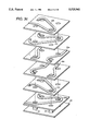
- FIGS. 5a-5f are perspective views illustrating the process of constructing the transformer of FIG. 1 in accordance with the present invention
- FIG. 5a shows machining of a step cavity
- FIG. 5b shows attachment of a ferromagnetic plate to the cavity
- FIG. 5c shows lamination of a dielectric layer over the ferromagnetic plate
- FIG. 5d shows application of a first metal layer to the dielectric layer
- FIGS. 6a and 6b illustrate staggered via interlayer connections and plated-through-hole interconnections, respectively, for making primary and secondary contacts on the surface of the top dielectric layer of a magnetic component according to the present invention
- FIGS. 7a-7f illustrate how an integrated transformer of the present invention may be connected to secondary side circuit elements in, for example, a power supply
- FIG. 7a is a circuit diagram of a simple secondary side circuit
- FIGS. 7b and 7c show a secondary-side interconnection scheme for the circuit of FIG. 9a
- FIGS. 7d-7f show alternative ways of interconnecting the transformer and secondary-side circuit elements.
- FIGS. 8e-8e illustrate differential plating steps according to the present invention
- FIG. 8a shows and HDI substrate with a layer of dielectric deposited thereon
- FIG. 8b shows a mask applied to the primary side circuit
- FIG. 8c shows additional planting
- FIG. 8d shows a portion of the metal layer etched away
- FIG. 8e shows removal of the mask from the primary side circuit and etching of the primary side metal layer to the desired conductor shape
- FIGS. 9a-9c illustrate differential plating steps according to an alternative embodiment of the present invention
- FIG. 9a shows a substrate with a dieletric layer and an etched thin metal layer on both primary and secondary circuits
- FIG. 9b shows application of a mask to the primary circuit
- FIG. 9c shows formation of thicker secondary side metal traces by electroless plating
- FIGS. 10a-10d illustrate differential plating steps according to another alternative embodiment of the present invention.
- FIG. 11 schematically illustrates an electromagnetic circuit component (e.g., a directional coupler) suitable for construction in an HDI structure in accordance with the present invention
- FIG. 10a shows a substrate with a dielectric layer and an etched thin metal layer on both primary and secondary circuits;
- FIG.10b shows masking of the primary side circuit;
- FIG 10c shows use of a shoring bar to apply additional metal to the secondary side circuit; and
- FIG. 10d shows the resulting HDI structure;
- FIG. 12 is an exploded, perspective view of an isolator for a microwave waveguide constructed in accordance with the present invention.
- FIG. 13 is an exploded, perspective view of an alternative embodiment of the isolator of FIG. 12.
- FIG. 1 illustrates a transformer 10 constructed in accordance with the present invention.
- Transformer 10 includes an HDI substrate 12 having a magnetic plate 14 embedded therein and alternating dielectric 16 and winding layers 18.
- magnetic plate 14 is described herein as comprising a ferromagnetic plate.
- Substrate 12 may comprise a ceramic or other suitable material.
- Through-holes 20 are provided for receiving core posts 22 of a top ferrite plate 24 upon completion of the transformer assembly.
- transformer 10 is illustrated as comprising a multi-pole (e.g., four-pole) winding structure.
- a multi-pole winding structure e.g., four-pole
- the present invention applies to single-pole winding structures as well.
- Suitable winding configurations are shown in the plan views of FIGS. 2a and 2b.
- Primary winding 25 of FIG. 2a is shown as having a total of four turns with a single turn around each of the four poles.
- each primary winding layer 25a and 25b has one-half turn around each pole, each turn being connected in series in circuit.
- a via 26 is used for connecting the two primary winding layers.
- FIG. 2b shows a single-layer secondary winding 27 with a single turn around each pole, all secondary turns being connected in parallel (not shown). The result is a transformer turns ratio of 4:1.
- FIG. 2c is an exploded, perspective view illustrating the winding layers of the pattern of FIG. 2a and 2b showing the alternating winding layers in the order as indicated in FIGS. 2a and 2b, i.e., 1st to 3rd.
- FIGS. 3a-3c Another suitable winding configuration is shown in FIGS. 3a-3c Similar suitable winding configurations are described in commonly assigned U.S. patent application Ser. No. 07/838,953 (docket RD-21,008) of Roshen et al. and in commonly assigned U.S. Patent application Ser. No. 07/838,958 (docket RD-21,748) of Yerman et al., both of which are incorporated by reference herein.
- Primary winding 29 of FIG. 3a is shown as having a total of eight turns with two turns around each of the four poles, all turns being connected in series. In each primary winding layer 29a-29d, there is one-half turn around each pole.
- FIG. 3b shows two secondary winding layers 30a and 30b, each having two turns which are connected in parallel. The result is a transformer turns ratio of 8:2 or 4:1, for this example.
- FIG. 3c is an exploded, perspective view of the windings of FIGS. 3a and 3b showing the alternating winding layers in the order as indicated in FIGS. 3a and 3b, i.e., 1st 6th.
- FIGS. 4a and 4b illustrate a spiral-type winding for a two-pole, two metal-layer design.
- multiple turns and current direction about poles 31 and 32 are shown for conductor layers 34 and 36 of FIG. 4b , with numeral 38 indicating the locations of vias for making connections between the winding layers.
- inductors with single windings may be constructed using embedded ferromagnetics in HDI structures according to the present invention.
- FIGS. 5a-5f illustrate the steps in constructing transformer 10 of FIG. 1 with windings 29 and 30 of FIGS. 3a -3c.
- a step cavity 40 is machined (e.g., by diamond milling, potting, stamping or other extraction methods) in ceramic substrate 12.
- ferromagnetic plate 14 which has been machined to fit within cavity 40, is attached to the cavity with a suitable adhesive, such as, for example, ULTEM 6000 glue manufactured by General Electric Company.
- a suitable adhesive such as, for example, ULTEM 6000 glue manufactured by General Electric Company.
- a non-conducting SPAN polymer manufactured by General Electric Company may be used to attach ferromagnetic plate 14 within cavity 40.
- thermosetting epoxy can be used which can be loaded with, for example, alumina or beryllia or aluminum nitride to achieve thermal conduction to the substrate.
- the epoxy could also be loaded with silver to achieve the same effect.
- ferromagnetic plate 14 may be inserted within the cavity without using an adhesive to attach it thereto, if desired.
- Ferromagnetic plate 14 may comprise, for example, a suitable ferrite such as, for example, MnZn or NiZn.
- An exemplary ferrite plate thickness is from approximately 0.02 to 0.03 inch.
- dielectric layer 16 is laminated over ferromagnetic plate 14 with an adhesive such as, for example, ULTEM 1000 glue manufactured by General Electric Company.
- a suitable dielectric comprises, for example, a polyimide film such as that sold under the name Kapton by E.I. du Pont de Nemours and Company.
- a first metal layer 18 is sputtered on the first Kapton polyimide film layer,.
- a suitable metal layer comprises copper or a combination of titanium and copper of thickness in the range, for example, from approximately 1000 to 2500 Angstroms.
- the metal layer is then electroplated to a desired thickness (e.g., approximately 0.001 inch).
- the metal layer is patterned, as shown in FIG. 5e, using photoresist masking and wet etching according to well-known methods.
- Another dielectric layer 16 (e.g., Kapton polyimide film) is laminated over the first winding layer.
- Primary winding vias 46 and secondary winding vias 48 (FIGS. 3a and 3b, respectively) are laser-drilled according to well-known methods to provide the illustrated winding patterns. Then, deposition of the second winding layer 18 occurs, as shown in FIG. 5f. The process continues until all winding layers are deposited and patterned within the HDI cavity.
- well-known meshed-based patterning and drilling methods such as reactive ion etching (RIE), may be used.
- RIE reactive ion etching
- an additional dielectric (Kapton polyimide film) layer may be laminated as a passivation layer. Then, a conformal metal mask is provided for patterning large through-holes 20 (FIG. 1). An excimer laser ablation can be used to drill holes 20 through to bottom ferrite plate 14. Alternatively, holes 20 may extend down only to a specified Kapton polyimide film layer in order to provide for an air gap in the magnetic circuit, as desired. In this way, a predetermined inductance may be achieved. Posts 22 are inserted into through-holes 20, and another Kapton polyimide film layer (not shown) is preferably laminated on top of plate 24 for further support of transformer 10 within cavity 40.
- Kapton polyimide film Kapton polyimide film
- contact pads 39 (FIG. 1) that may be either recessed, as shown, or on the top surface of the last dielectric layer using either staggered via interlayer connections 41, as illustrated in FIG. 6a, or plated-through-hole interconnections 43, as illustrated in FIG. 6b.
- FIGS. 7a-7f illustrate how an integrated transformer according to the present invention can be connected to secondary side circuit elements in, for example, a power supply.
- FIG. 7a is a circuit diagram of a simple secondary side circuit comprising a diode rectifier D and a filter capacitor C with two output terminals, +V and ground.
- FIGS. 7b and 7c show a secondary-side interconnection scheme for an HDI circuit including a transformer 10 having terminations 60 at the top thereof.
- Two metal layers 50 and 52, with dielectric layers 53 used for insulation thereof, are used for connection to diode D (FIG. 7c ) and capacitor C (FIG. 7b ).
- Metal layer 50 is deposited directly on ceramic substrate 12 and forms part of the ground terminal of the power supply.
- Metal layer 50 connects the transformer, the diode and the capacitor through metallized vias 56 to metal layer 52.
- Metal layer 52 also serves as the +V (power) output terminal of the power supply.
- very low inductance connections are thus made to secondary side circuit elements.
- FIGS. 7d, 7e and 7f show alternative ways of interconnecting transformer 10 and secondary side circuit elements (e.g., capacitor C and diode D of FIG. 7a) wherein the terminations 60' of the transformer are recessed below the top surface of the transformer.
- two metal overlayers 50' and 52 are used in combination with vias 56 to make the interconnections and to provide the output terminals (power and ground planes) of the power supply.
- those of FIGS. 7d-7f have very low inductance.
- the secondary side interconnections in a power supply typically carry substantially heavier current than those of the primary side circuit (not shown).
- thicker metallization is needed for the secondary side interconnections and output terminals.
- a process of differential plating is employed to obtain the desired metal thickness on the two metal overlayers 50 (or 50') and 52 shown in FIGS. 7b-7f. Since a thicker metal layer is needed on the secondary side of the circuit to accommodate the higher secondary side circuit, a mask is used on the primary side circuit such that additional metal is deposited only on the secondary portion of the metal layer.
- the purposes of differential plating according to the present invention are: (1) to minimize losses by matching the skin depth of high frequency circuitry to conductor thickness; (2) to optimize the design rules for fabricating the HDI circuits; and (3) to minimize losses for low frequency dc resistances.
- FIGS. 8e-8e illustrate the steps in differential plating of an HDI circuit according to the present invention.
- FIGS. 8e-8e show differential plating of primary and secondary side HDI circuits.
- the differential plating method of the present invention may be employed in the fabrication of a single component by varying the thicknesses of different layers or other portions thereof.
- FIG. 8a shows HDI substrate 12 with a layer of dielectric 16 (e.g., Kapton polyimide film) and a layer of thin metal 18 (e.g., copper or a combination of copper and titanium) deposited thereon.
- a process of subtractive differential plating is employed as follows.
- a mask 80 is applied to the primary side circuit.
- FIG. 8c shows additional plating 18b added to thin metal layer 18a (formerly 18). Together, layers 18a and 18b are represented by the numeral 18'.
- FIG. 8e shows the results after mask 80 is removed from the primary side circuit, and the primary side metal layer is etched to the desired conductor shape.
- FIGS. 9a-9c illustrate differential plating according to an alternative embodiment of the present invention, i.e., involving an additive process.
- Substrate 12 is shown in FIG. 9a with dielectric layer 16 and an etched thin metal layer 18 on both the primary and secondary circuits.
- a mask 80 is applied to the primary side of the circuit, and in FIG. 9c, the secondary side metal traces are made thicker by electroless plating of additional metal thereon to form the thicker layer 18'.
- FIGS. 10a-10d illustrate differential plating according to another alternative embodiment which also involves an additive plating process.
- Substrate 12 is shown in FIG. 10a with dielectric layer 16 and an etched thin metal layer 18 on both the primary and secondary sides of the HDI circuit.
- the secondary side circuit includes a shorting bar 82 of a type used in well-known electroplating processes.
- the primary side circuit is masked.
- the secondary side circuit is electroplated to apply additional metal layer 18b to layer 18a.
- FIG. 10d shows the HDI structure with the mask and the shorting bar removed.
- uniformly plated interconnections may be desirable for many other applications.
- uniform electroplating may be advantageous due to: planarity of the metal layers; lower dc and ac losses; and more compact primary side circuitry as thinner metal traces can be used.
- FIG. 11 schematically illustrates a distributed electromagnetic circuit component (e.g., a directional coupler) suitable for construction using HDI technology in accordance with the present invention.
- the invention is not limited to directional couplers, but applies to any suitable distributed electromagnetic circuit component, such as, for example, isolators, waveguides, phase-shifters and circulators, and so on.
- a distributed electromagnetic circuit component has a distributed electromagnetic field due to both electric and magnetic coupling therein so as to provide distributed wave propagation in either or both a forward and reverse direction.
- the wavelength of propagation in a distributed electromagnetic component is smaller than the effective component size, as opposed to a lumped magnetic component, such as those described hereinabove, which has a wavelength greater than the effective component size.
- FIG. 11 illustrates a directional coupler 110 having a predetermined parasitic capacitance Cp.
- coupler 10 is shown as being coupled to external circuitry, including capacitors C, diodes D and resistors R, for example.
- the coupler of FIG. 11 is constructed in similar manner as the transformer of FIG. 1.
- coupler 110 is constructed to have a predetermined parasitic capacitance Cp.
- differential plating of the metal thickness between primary and secondary winding layers yields a defined point in the coupler transformer at which the capacitive coupling Cp exists, as illustrated in FIG. 11.
- FIG. 12 illustrates another application of an electromagnetic HDI structure according to the present invention comprising an isolator 100 for a microwave waveguide 102.
- magnetic plate 14 is situated within a cavity within HDI substrate 12.
- a dielectric layer 16 is applied to magnetic plate 14.
- the top and bottom of waveguide 102 comprise metal layers 18 which are connected together by vias 104.
- vias 104 are illustrated as comprising trench vias. However, multiple vias (not shown) may be alternatively employed.
- Another dielectric layer 16' is disposed between the top and bottom metal layers and comprises the waveguide cavity.
- a magnetic top plate 24' has sides 108 such that it fits around the microwave waveguide within the HDI cavity in substrate 12.
- FIG. 13 illustrates an alternative embodiment (110) of the isolator of FIG. 12.
- a ferromagnetic insert 112 is employed instead of the magnetic top and bottom plates, 108 and 14, respectively of FIG. 12.
- operation of isolator 100 of FIG. 12 and isolator 110 of FIG. 13 is in a similar manner.
Abstract
Description
Claims (26)
Priority Applications (5)
| Application Number | Priority Date | Filing Date | Title |
|---|---|---|---|
| US08/043,166 US5525941A (en) | 1993-04-01 | 1993-04-01 | Magnetic and electromagnetic circuit components having embedded magnetic material in a high density interconnect structure |
| EP94302198A EP0618595A1 (en) | 1993-04-01 | 1994-03-28 | Magnetic and electromagnetic circuit components having embedded magnetic material in a high density interconnect structure |
| JP6061850A JPH0714714A (en) | 1993-04-01 | 1994-03-31 | Hdi circuit parts |
| CA002120452A CA2120452A1 (en) | 1993-04-01 | 1994-03-31 | Magnetic and electromagnetic circuit components having embedded magnetic material in a high density interconnect structure |
| US08/588,525 US5745981A (en) | 1993-04-01 | 1996-01-18 | Method for making magnetic and electromagnetic circuit components having embedded magnetic materials in a high density interconnect structure |
Applications Claiming Priority (1)
| Application Number | Priority Date | Filing Date | Title |
|---|---|---|---|
| US08/043,166 US5525941A (en) | 1993-04-01 | 1993-04-01 | Magnetic and electromagnetic circuit components having embedded magnetic material in a high density interconnect structure |
Related Child Applications (1)
| Application Number | Title | Priority Date | Filing Date |
|---|---|---|---|
| US08/588,525 Division US5745981A (en) | 1993-04-01 | 1996-01-18 | Method for making magnetic and electromagnetic circuit components having embedded magnetic materials in a high density interconnect structure |
Publications (1)
| Publication Number | Publication Date |
|---|---|
| US5525941A true US5525941A (en) | 1996-06-11 |
Family
ID=21925830
Family Applications (2)
| Application Number | Title | Priority Date | Filing Date |
|---|---|---|---|
| US08/043,166 Expired - Lifetime US5525941A (en) | 1993-04-01 | 1993-04-01 | Magnetic and electromagnetic circuit components having embedded magnetic material in a high density interconnect structure |
| US08/588,525 Expired - Lifetime US5745981A (en) | 1993-04-01 | 1996-01-18 | Method for making magnetic and electromagnetic circuit components having embedded magnetic materials in a high density interconnect structure |
Family Applications After (1)
| Application Number | Title | Priority Date | Filing Date |
|---|---|---|---|
| US08/588,525 Expired - Lifetime US5745981A (en) | 1993-04-01 | 1996-01-18 | Method for making magnetic and electromagnetic circuit components having embedded magnetic materials in a high density interconnect structure |
Country Status (4)
| Country | Link |
|---|---|
| US (2) | US5525941A (en) |
| EP (1) | EP0618595A1 (en) |
| JP (1) | JPH0714714A (en) |
| CA (1) | CA2120452A1 (en) |
Cited By (13)
| Publication number | Priority date | Publication date | Assignee | Title |
|---|---|---|---|---|
| US5783879A (en) * | 1997-06-03 | 1998-07-21 | Eastman Kodak Company | Micromotor in a ceramic substrate |
| US5821846A (en) * | 1995-05-22 | 1998-10-13 | Steward, Inc. | High current ferrite electromagnetic interference suppressor and associated method |
| US6177806B1 (en) * | 1997-09-03 | 2001-01-23 | International Business Machines Corp. | Signal sensor for rf integrated systems |
| US6291272B1 (en) | 1999-12-23 | 2001-09-18 | International Business Machines Corporation | Structure and process for making substrate packages for high frequency application |
| US6466454B1 (en) * | 1999-05-18 | 2002-10-15 | Ascom Energy Systems Ag | Component transformer |
| US6514047B2 (en) | 2001-05-04 | 2003-02-04 | Macrosonix Corporation | Linear resonance pump and methods for compressing fluid |
| US20120249273A1 (en) * | 2008-10-20 | 2012-10-04 | Skyworks Solutions, Inc. | Magnetic-dielectric assembly |
| US20120293150A1 (en) * | 2008-03-28 | 2012-11-22 | Broadcom Corporation | IC Package with Embedded Transformer |
| US20160125997A1 (en) * | 2014-10-31 | 2016-05-05 | Hyundai Mobis Co., Ltd. | Apparatus for dissipating heat of inductor |
| US9601468B2 (en) * | 2013-08-13 | 2017-03-21 | Intel Corporation | Magnetic contacts |
| US9893008B2 (en) * | 2013-08-06 | 2018-02-13 | Texas Instruments Incorporated | High voltage polymer dielectric capacitor isolation device |
| US20190206613A1 (en) * | 2017-12-28 | 2019-07-04 | Realtek Semiconductor Corp. | High isolation integrated inductor and method therof |
| CN114005653A (en) * | 2020-07-28 | 2022-02-01 | 华为技术有限公司 | Transformer, switching power supply and communication equipment |
Families Citing this family (36)
| Publication number | Priority date | Publication date | Assignee | Title |
|---|---|---|---|---|
| US5558091A (en) * | 1993-10-06 | 1996-09-24 | Biosense, Inc. | Magnetic determination of position and orientation |
| US5781091A (en) * | 1995-07-24 | 1998-07-14 | Autosplice Systems Inc. | Electronic inductive device and method for manufacturing |
| US6896826B2 (en) * | 1997-01-09 | 2005-05-24 | Advanced Technology Materials, Inc. | Aqueous cleaning composition containing copper-specific corrosion inhibitor for cleaning inorganic residues on semiconductor substrate |
| US6440750B1 (en) | 1997-06-10 | 2002-08-27 | Agere Systems Guardian Corporation | Method of making integrated circuit having a micromagnetic device |
| US6118351A (en) * | 1997-06-10 | 2000-09-12 | Lucent Technologies Inc. | Micromagnetic device for power processing applications and method of manufacture therefor |
| EP0926689A3 (en) * | 1997-12-18 | 1999-12-01 | National University of Ireland, Cork | Magnetic components and their production |
| US6105236A (en) * | 1998-02-05 | 2000-08-22 | Raytheon Company | Magnetic structure for minimizing AC resistance in planar rectangular conductors |
| FR2779576B1 (en) * | 1998-06-05 | 2001-04-27 | Thomson Csf | MICRO-ELECTRONIC MICRO-ELECTRONIC MODULE COMPRISING TWO DIFFERENT SUBSTRATE MATERIALS AND METHOD FOR MANUFACTURING SUCH A MODULE |
| DE19854234C1 (en) * | 1998-11-24 | 2000-06-21 | Bosch Gmbh Robert | Inductive component with a planar line structure and method for producing the same |
| US6255714B1 (en) | 1999-06-22 | 2001-07-03 | Agere Systems Guardian Corporation | Integrated circuit having a micromagnetic device including a ferromagnetic core and method of manufacture therefor |
| DE19945855A1 (en) * | 1999-09-24 | 2001-03-29 | Bosch Gmbh Robert | High inductance micro-coil constructed on substrate, useful at higher currents is formed using additive- or doping technology with diamond or diamond-like material in insulator |
| US6493861B1 (en) * | 1999-12-28 | 2002-12-10 | Intel Corporation | Interconnected series of plated through hole vias and method of fabrication therefor |
| US7305355B2 (en) * | 2000-06-12 | 2007-12-04 | American Express Travel Related Services Company, Inc. | Universal shopping cart and order injection system |
| JPWO2002075853A1 (en) * | 2001-03-15 | 2004-07-08 | 松下電器産業株式会社 | Antenna device |
| US6704248B1 (en) | 2001-05-25 | 2004-03-09 | Lockheed Martin Corporation | High density power module incorporating passive components distributed in a substrate |
| US6778043B2 (en) * | 2001-12-19 | 2004-08-17 | Maxxan Systems, Inc. | Method and apparatus for adding inductance to printed circuits |
| WO2004010532A1 (en) | 2002-07-15 | 2004-01-29 | Fractus, S.A. | Antenna with one or more holes |
| JP2004128932A (en) | 2002-10-03 | 2004-04-22 | Matsushita Electric Ind Co Ltd | Antenna assembly |
| TWI227502B (en) * | 2003-09-02 | 2005-02-01 | Ind Tech Res Inst | Precise multi-pole magnetic components and manufacturing method thereof |
| WO2006123482A1 (en) * | 2005-05-20 | 2006-11-23 | Murata Manufacturing Co., Ltd. | Multilayer directional coupler |
| WO2011014200A1 (en) * | 2009-07-31 | 2011-02-03 | Radial Electronics, Inc | Embedded magnetic components and methods |
| JP2007123982A (en) | 2005-10-25 | 2007-05-17 | Sony Ericsson Mobilecommunications Japan Inc | Multiband compatible antenna system and communication terminal |
| EP2109867A4 (en) | 2007-01-11 | 2014-12-24 | Keyeye Comm | Wideband planar transformer |
| US8203418B2 (en) * | 2007-01-11 | 2012-06-19 | Planarmag, Inc. | Manufacture and use of planar embedded magnetics as discrete components and in integrated connectors |
| US20090153281A1 (en) * | 2007-12-13 | 2009-06-18 | Ahmadreza Rofougaran | Method and system for an integrated circuit package with ferri/ferromagnetic layers |
| JP5685815B2 (en) * | 2009-03-16 | 2015-03-18 | Tdk株式会社 | Transformer and switching power supply |
| US8089331B2 (en) * | 2009-05-12 | 2012-01-03 | Raytheon Company | Planar magnetic structure |
| US20130119511A1 (en) * | 2011-11-10 | 2013-05-16 | Taiwan Semiconductor Manufacturing Company, Ltd. | Inductor having bond-wire and manufacturing method thereof |
| EP3120360A1 (en) * | 2014-03-19 | 2017-01-25 | Rompower Energy Systems, Inc. | Magnetic structures for low leakage inductance and very high efficiency |
| US9520793B2 (en) | 2014-09-22 | 2016-12-13 | Raytheon Company | Stacked power converter assembly |
| US10050438B2 (en) | 2015-10-16 | 2018-08-14 | Raytheon Company | Stacked power converter assembly |
| US10049810B2 (en) | 2015-11-09 | 2018-08-14 | Raytheon Company | High voltage high frequency transformer |
| US10050533B2 (en) | 2016-07-26 | 2018-08-14 | Raytheon Company | High voltage high frequency transformer |
| US10672553B2 (en) | 2017-05-10 | 2020-06-02 | Raytheon Company | High voltage high frequency transformer |
| US11694832B2 (en) | 2019-02-01 | 2023-07-04 | Raytheon Company | High voltage high frequency transformer |
| CN116612960B (en) * | 2023-07-21 | 2023-12-12 | 深圳平创半导体有限公司 | LLC magnetic integration high-frequency transformer |
Citations (6)
| Publication number | Priority date | Publication date | Assignee | Title |
|---|---|---|---|---|
| US3148356A (en) * | 1959-09-14 | 1964-09-08 | Jr George A Hedden | Printed circuit connector |
| US4626816A (en) * | 1986-03-05 | 1986-12-02 | American Technical Ceramics Corp. | Multilayer series-connected coil assembly on a wafer and method of manufacture |
| US5017894A (en) * | 1989-02-01 | 1991-05-21 | Hitachi Ferrite, Ltd. | Lumped constant non-reciprocal circuit element |
| US5126715A (en) * | 1990-07-02 | 1992-06-30 | General Electric Company | Low-profile multi-pole conductive film transformer |
| US5257000A (en) * | 1992-02-14 | 1993-10-26 | At&T Bell Laboratories | Circuit elements dependent on core inductance and fabrication thereof |
| US5349743A (en) * | 1991-05-02 | 1994-09-27 | At&T Bell Laboratories | Method of making a multilayer monolithic magnet component |
Family Cites Families (3)
| Publication number | Priority date | Publication date | Assignee | Title |
|---|---|---|---|---|
| JPH04206607A (en) * | 1990-11-30 | 1992-07-28 | Hitachi Maxell Ltd | Thin-film transformer/inductor |
| US5126714A (en) * | 1990-12-20 | 1992-06-30 | The United States Of America As Represented By The Secretary Of The Navy | Integrated circuit transformer |
| GB2252208B (en) * | 1991-01-24 | 1995-05-03 | Burr Brown Corp | Hybrid integrated circuit planar transformer |
-
1993
- 1993-04-01 US US08/043,166 patent/US5525941A/en not_active Expired - Lifetime
-
1994
- 1994-03-28 EP EP94302198A patent/EP0618595A1/en not_active Withdrawn
- 1994-03-31 JP JP6061850A patent/JPH0714714A/en not_active Withdrawn
- 1994-03-31 CA CA002120452A patent/CA2120452A1/en not_active Abandoned
-
1996
- 1996-01-18 US US08/588,525 patent/US5745981A/en not_active Expired - Lifetime
Patent Citations (6)
| Publication number | Priority date | Publication date | Assignee | Title |
|---|---|---|---|---|
| US3148356A (en) * | 1959-09-14 | 1964-09-08 | Jr George A Hedden | Printed circuit connector |
| US4626816A (en) * | 1986-03-05 | 1986-12-02 | American Technical Ceramics Corp. | Multilayer series-connected coil assembly on a wafer and method of manufacture |
| US5017894A (en) * | 1989-02-01 | 1991-05-21 | Hitachi Ferrite, Ltd. | Lumped constant non-reciprocal circuit element |
| US5126715A (en) * | 1990-07-02 | 1992-06-30 | General Electric Company | Low-profile multi-pole conductive film transformer |
| US5349743A (en) * | 1991-05-02 | 1994-09-27 | At&T Bell Laboratories | Method of making a multilayer monolithic magnet component |
| US5257000A (en) * | 1992-02-14 | 1993-10-26 | At&T Bell Laboratories | Circuit elements dependent on core inductance and fabrication thereof |
Non-Patent Citations (8)
| Title |
|---|
| A. Yerman et al., "Z-Foldable Secondary Winding for a Low-Profile, Multi-Pole Transformer", Ser. No. 07/838,958, filed Feb. 21, 1992. |
| A. Yerman et al., Z Foldable Secondary Winding for a Low Profile, Multi Pole Transformer , Ser. No. 07/838,958, filed Feb. 21, 1992. * |
| Crawford, D. J. et al; "Etched Transformer"; IBM Technical Disclosure Bulletin; vol. 8, No. 5; Oct. 1965; p. 723. |
| Crawford, D. J. et al; Etched Transformer ; IBM Technical Disclosure Bulletin; vol. 8, No. 5; Oct. 1965; p. 723. * |
| W. Roshen et al., "High-Frequency Low-Profile Inductor", Ser. No. 07/838,656, filed Feb. 20, 1992. |
| W. Roshen et al., "Transfomer with Center-Tapped Secondary", Ser. No. 07/838,953, filed Feb. 21, 1992. |
| W. Roshen et al., High Frequency Low Profile Inductor , Ser. No. 07/838,656, filed Feb. 20, 1992. * |
| W. Roshen et al., Transfomer with Center Tapped Secondary , Ser. No. 07/838,953, filed Feb. 21, 1992. * |
Cited By (19)
| Publication number | Priority date | Publication date | Assignee | Title |
|---|---|---|---|---|
| US5821846A (en) * | 1995-05-22 | 1998-10-13 | Steward, Inc. | High current ferrite electromagnetic interference suppressor and associated method |
| US6107907A (en) * | 1995-05-22 | 2000-08-22 | Steward, Inc. | High current ferrite electromagnetic interference supressor and associated method |
| US5783879A (en) * | 1997-06-03 | 1998-07-21 | Eastman Kodak Company | Micromotor in a ceramic substrate |
| US6177806B1 (en) * | 1997-09-03 | 2001-01-23 | International Business Machines Corp. | Signal sensor for rf integrated systems |
| US6452413B1 (en) | 1997-09-03 | 2002-09-17 | Ibm Corporation | Signal sensor for rf integrated systems |
| US6466454B1 (en) * | 1999-05-18 | 2002-10-15 | Ascom Energy Systems Ag | Component transformer |
| US6291272B1 (en) | 1999-12-23 | 2001-09-18 | International Business Machines Corporation | Structure and process for making substrate packages for high frequency application |
| US6514047B2 (en) | 2001-05-04 | 2003-02-04 | Macrosonix Corporation | Linear resonance pump and methods for compressing fluid |
| US8912639B2 (en) * | 2008-03-28 | 2014-12-16 | Broadcom Corporation | IC package with embedded transformer |
| US20120293150A1 (en) * | 2008-03-28 | 2012-11-22 | Broadcom Corporation | IC Package with Embedded Transformer |
| US20120249273A1 (en) * | 2008-10-20 | 2012-10-04 | Skyworks Solutions, Inc. | Magnetic-dielectric assembly |
| US9893008B2 (en) * | 2013-08-06 | 2018-02-13 | Texas Instruments Incorporated | High voltage polymer dielectric capacitor isolation device |
| US9601468B2 (en) * | 2013-08-13 | 2017-03-21 | Intel Corporation | Magnetic contacts |
| US20160125997A1 (en) * | 2014-10-31 | 2016-05-05 | Hyundai Mobis Co., Ltd. | Apparatus for dissipating heat of inductor |
| US20190206613A1 (en) * | 2017-12-28 | 2019-07-04 | Realtek Semiconductor Corp. | High isolation integrated inductor and method therof |
| CN109979913A (en) * | 2017-12-28 | 2019-07-05 | 瑞昱半导体股份有限公司 | High-isolation integrated inductor and its manufacturing method |
| US11328859B2 (en) * | 2017-12-28 | 2022-05-10 | Realtek Semiconductor Corp. | High isolation integrated inductor and method therof |
| CN114005653A (en) * | 2020-07-28 | 2022-02-01 | 华为技术有限公司 | Transformer, switching power supply and communication equipment |
| CN114005653B (en) * | 2020-07-28 | 2023-11-10 | 华为技术有限公司 | Transformer, switching power supply and communication equipment |
Also Published As
| Publication number | Publication date |
|---|---|
| EP0618595A1 (en) | 1994-10-05 |
| JPH0714714A (en) | 1995-01-17 |
| US5745981A (en) | 1998-05-05 |
| CA2120452A1 (en) | 1994-10-02 |
Similar Documents
| Publication | Publication Date | Title |
|---|---|---|
| US5525941A (en) | Magnetic and electromagnetic circuit components having embedded magnetic material in a high density interconnect structure | |
| US5898991A (en) | Methods of fabrication of coaxial vias and magnetic devices | |
| US7127808B2 (en) | Spiral couplers manufactured by etching and fusion bonding | |
| EP0643403B1 (en) | Inductive structures for semiconductor integrated circuits | |
| US5541567A (en) | Coaxial vias in an electronic substrate | |
| US7280024B2 (en) | Integrated transformer structure and method of fabrication | |
| US5850682A (en) | Method of manufacturing chip-type common mode choke coil | |
| US6501363B1 (en) | Vertical transformer | |
| US5321380A (en) | Low profile printed circuit board | |
| KR100917508B1 (en) | High-frequency module board device | |
| US6073339A (en) | Method of making low profile pin-less planar magnetic devices | |
| US7599190B2 (en) | High-frequency module, and method of producing same | |
| US5576680A (en) | Structure and fabrication process of inductors on semiconductor chip | |
| US5487214A (en) | Method of making a monolithic magnetic device with printed circuit interconnections | |
| US5559363A (en) | Off-chip impedance matching utilizing a dielectric element and high density interconnect technology | |
| KR100949224B1 (en) | Filter circuit apparatus and manufacturing method thereof | |
| US20030148739A1 (en) | High-frequency module device | |
| WO2000074142A1 (en) | Multiple level spiral inductors used to form a filter in a printed circuit board | |
| WO2003100853A1 (en) | Multilayer substrate with built-in coil, semiconductor chip, methods for manufacturing them | |
| US6774743B2 (en) | Multi-layered spiral couplers on a fluropolymer composite substrate | |
| KR20010093792A (en) | Microwave mixer with baluns having rectangular coaxial transmission line | |
| US5812038A (en) | Volume efficient resonator | |
| US5757623A (en) | Low-noise, high-Q stripline inductor | |
| JP2003283284A (en) | Flat filter | |
| JPS62142395A (en) | Multi-function circuit board |
Legal Events
| Date | Code | Title | Description |
|---|---|---|---|
| AS | Assignment |
Owner name: GENERAL ELECTRIC COMPANY, NEW YORK Free format text: ASSIGNMENT OF ASSIGNORS INTEREST.;ASSIGNORS:ROSHEN, WASEEM A.;KORMAN, CHARLES S.;DAUM, WOLFGANG;REEL/FRAME:006521/0210 Effective date: 19930318 |
|
| STPP | Information on status: patent application and granting procedure in general |
Free format text: APPLICATION UNDERGOING PREEXAM PROCESSING |
|
| FEPP | Fee payment procedure |
Free format text: PAYOR NUMBER ASSIGNED (ORIGINAL EVENT CODE: ASPN); ENTITY STATUS OF PATENT OWNER: LARGE ENTITY |
|
| FPAY | Fee payment |
Year of fee payment: 4 |
|
| REMI | Maintenance fee reminder mailed | ||
| REIN | Reinstatement after maintenance fee payment confirmed | ||
| FP | Lapsed due to failure to pay maintenance fee |
Effective date: 20040611 |
|
| FEPP | Fee payment procedure |
Free format text: PETITION RELATED TO MAINTENANCE FEES FILED (ORIGINAL EVENT CODE: PMFP); ENTITY STATUS OF PATENT OWNER: LARGE ENTITY |
|
| FEPP | Fee payment procedure |
Free format text: PETITION RELATED TO MAINTENANCE FEES GRANTED (ORIGINAL EVENT CODE: PMFG); ENTITY STATUS OF PATENT OWNER: LARGE ENTITY |
|
| FPAY | Fee payment |
Year of fee payment: 8 |
|
| SULP | Surcharge for late payment | ||
| PRDP | Patent reinstated due to the acceptance of a late maintenance fee |
Effective date: 20060919 |
|
| REMI | Maintenance fee reminder mailed | ||
| FPAY | Fee payment |
Year of fee payment: 12 |