US5541532A - All MOS single-ended to differential level converter - Google Patents
All MOS single-ended to differential level converter Download PDFInfo
- Publication number
- US5541532A US5541532A US08/516,384 US51638495A US5541532A US 5541532 A US5541532 A US 5541532A US 51638495 A US51638495 A US 51638495A US 5541532 A US5541532 A US 5541532A
- Authority
- US
- United States
- Prior art keywords
- ended
- semiconductors
- pmos
- level converter
- mos
- Prior art date
- Legal status (The legal status is an assumption and is not a legal conclusion. Google has not performed a legal analysis and makes no representation as to the accuracy of the status listed.)
- Expired - Lifetime
Links
Images


Classifications
-
- H—ELECTRICITY
- H03—ELECTRONIC CIRCUITRY
- H03K—PULSE TECHNIQUE
- H03K19/00—Logic circuits, i.e. having at least two inputs acting on one output; Inverting circuits
- H03K19/0175—Coupling arrangements; Interface arrangements
- H03K19/0185—Coupling arrangements; Interface arrangements using field effect transistors only
- H03K19/018507—Interface arrangements
- H03K19/018521—Interface arrangements of complementary type, e.g. CMOS
- H03K19/018528—Interface arrangements of complementary type, e.g. CMOS with at least one differential stage
-
- H—ELECTRICITY
- H03—ELECTRONIC CIRCUITRY
- H03K—PULSE TECHNIQUE
- H03K19/00—Logic circuits, i.e. having at least two inputs acting on one output; Inverting circuits
- H03K19/003—Modifications for increasing the reliability for protection
- H03K19/00369—Modifications for compensating variations of temperature, supply voltage or other physical parameters
- H03K19/00384—Modifications for compensating variations of temperature, supply voltage or other physical parameters in field effect transistor circuits
Definitions
- This invention relates to an improved all MOS single ended to differential level converter with minimum distortion.
- a digital processor receives a digital input from, for example, a microcontroller or a P.C. and provides a single ended digital output to a level converter.
- the level converter then provides an analog differential signal to an analog differential processor such as for example a precision delay line in the write channel of a disc drive.
- the level converter receives the single ended input from the digital processor and transforms it to an analog differential signal compatible with the differential signal processor input.
- the analog differential processor began to be constructed with CMOS technology to reduce cost the level converter too was made using CMOS technology and major distortions occurred in the output signal to the analog differential process. These were not a major inconvenience, however, since the distortion, namely spikes, had time to settle without disrupting the subsequent processing.
- the digital processor, level converter, and analog differential processor are all implemented on CMOS on a single chip and the time scale has accelerated to the point where there is not time for the spikes to settle and so the signal processing is seriously degraded.
- the invention results from the realization that certain signal distortion in an all MOS single ended to differential level converter was the result of the differentially converted NMOS semiconductors being simultaneously off for a period of time each cycle and that this could be avoided and the distortion dramatically reduced by using PMOS semiconductors in combination with or in place of the NMOS semiconductors to overlap the on-time rather than the off-time.
- This invention features an all MOS single-ended to differential level converter including first and second source follower circuits each including first and second PMOS semiconductors each having a drain, a source and a gate electrode. There is a current source commonly connected to the drain electrodes of the first and second PMOS semiconductors and an input circuit provides to one of the gate electrodes a single-ended input signal and to the other an inverted single-ended input signal. There are first and second load impedances connected to the source electrodes of the first and second PMOS semiconductors, respectively, for providing output analog differential signals at a level which is a function of the load impedances and current source magnitude.
- the current source may be an NMOS semiconductor with-its drain electrode connected to the drain electrodes of the first and second semiconductors.
- the input circuit may include two channels one connected to each of the gate electrodes of the first and second PMOS semiconductors, one of the channels including an inverter and the other including a non-inverting transmission gate for propagation delay equalization.
- the first and second load impedances may include third and fourth PMOS semiconductors, respectively. There may also be included a replica bias circuit for biasing the third and fourth PMOS semiconductors.
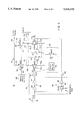
- FIG. 1 is a functional block diagram of an all MOS single-ended to differential level converter of this invention in a disc drive read/write integrated circuit;
- FIG. 2 is a schematic diagram of a prior art all MOS single-ended to differential level converter
- FIG. 3 is an enlarged diagrammatic view of a portion of the switching waveforms showing the cause of the distortions in the prior art level converter circuit of FIG. 2;
- FIG. 4 depicts the input waveforms that drive the prior art level converter of FIG.
- FIG. 5 depicts the output waveterms produced by the level converter of FIG. 2 displaying the substantial distortion which occurs in prior art all MOS level converters;
- FIG. 6 is an all MOS single-ended differential level converter according to this invention.
- FIG. 7 is an enlarged diagrammatic view of a portion of the switching waveforms that operate the level converter of FIG. 6;
- FIG. 8 depicts the input waveforms that drive the level converter of FIG. 6;
- FIG. 9 depicts the output waveforms produced by the level converter of FIG. 6 virtually without distortion.
- FIG. 10 is a schematic diagram of an all MOS implementation of the single-ended to differential level converter according to this invention.
- FIG. 1 a disc drive read/write all MOS integrated circuit 10 including a digital signal processing section 12 which could be an encoder or similar device which receives signals from a microcontroller or PC. Its output, a single-ended large magnitude digital-like signal 14, is provided to the all MOS single-ended differential level converter 16 according to this invention.
- Converter 16 receives the single-ended input 14 and produces a differential analog signal of small or reduced magnitude 18 as input to differential analog signal processing section 20 which may for example be a precision delay line in the write channel of this device.
- Prior art level converter 16a includes differential amplifier 22 which includes two inverters (KJM) which include two NMOS semiconductors 24 and 26 whose source electrodes 28 and 30 are commonly connected to current source 32.
- Current source 32 includes NMOS semiconductor 34 and a current bias circuit 36.
- the drain electrodes 38 and 40 of NMOS semiconductors 24 and 26, respectively, are connected to outputs 42 and 44 and to load impedances 46 and 48.
- Load impedances 46 and 48 are actually replica biased PMOS semiconductors having their drains 50, 52 connected to drains 38 and 40 of NMOS semiconductors 24 and 26, respectively, and their sources 54 and 56 commonly connected to supply voltage 58.
- Replica biasing circuit 59 as is well known in the art is used to bias the gates 60 and 62 of semiconductors 46 and 48.
- Circuit 76 includes a normal channel 78 and an inverting channel 80.
- Normal channel 78 provides input 74 to gate 70 in the normal non-inverted form.
- Channel 80 through the use of inverter 82 provides input signal 84 to gate 70.
- Inverting channel 80 through inverter 82 provides input signal 84 in its inverted form 86, FIG. 3, to gate 72.
- an inverting amplifier 88 corresponding to amplifier 82 is required.
- this inverts input signal 84 so a second inverter amplifier 90 is used so that the signal is twice inverted and is delivered in the positive form 84 that is present at input 74.
- a transmission gate 92 is used to provide propagation equalization corresponding to inverting amplifier 90 without the inversion.
- replica bias circuit 59 provides a bias to gates 60 and 62 so that PMOS semiconductors 46 and 48 act as a load impedance to control the swing below the supply voltage 58 when NMOS semiconductors 24 and 26 are alternately conducting.
- PMOS semiconductors 46 and 48 could in fact be replaced by simple impedances or resistances if the accuracy of those elements were sufficient.
- replica bias circuits are used to drive MOS semiconductors to provide the requisite precision impedance.
- parasitic capacitance 110 is being charge pumped so that drain 38 of semiconductor 24 is driven to a voltage above the supply voltage on line 58. As soon as point 105 is reached and semiconductor 24 begins to conduct, that voltage drops dramatically. This action generates a positive going spike which causes a substantial distortion in the output signal on lines 42 and 44. A similar negative going but somewhat smaller spike is occasioned by the attempt of current source 32 to draw down point 104 toward ground, followed by its abrupt return in the positive direction when semiconductor 24 begins to conduct. Similar distortions are incurred alternately during the corresponding operation of semiconductor 26.
- FIGS. 4 and 5 The substantiality of the distortion can be seen from FIGS. 4 and 5 where in FIG. 4 there is depicted the input signals 84 in solid line and 86 in dashed line, which are relatively clean signals.
- FIG. 5 the distorted outputs 42 in solid and 44 in phantom, are shown.
- the positive-going spike 120 occasioned by the charge pumping of the parasitic capacitor 110 and the negative-going spike 122 which occurs because of the attempt by the current source 32 to pull down point 104 toward ground and then the abrupt positive return of the signal when semiconductor 24 finally conducts at point 104, FIG. 3.
- Similar distortion occurs with respect to semiconductor 26 and parasitic capacitor 111.
- the threshold 100 which establishes points 103 and 105 is referenced to ground 107. Since it is referenced to ground its relative position with respect to the upper rail or supply voltage 58 is dependent upon the area of the device on the integrated circuit wafer and also on the level of the supply voltage which may fluctuate due to external conditions.
- the circuit of FIG. 2 is modified in a simple but elegant fashion to remove or reduce the distortion shown in FIG. 5 by simply replacing the NMOS semiconductors 24 and 26 of prior art system 16a with the PMOS semiconductors 24a and 26a of level converter 16, FIG. 6, according to this invention.
- the gates 70a, 72a of PMOS semiconductors 24a and 26a receive the same signals 84, the normal signal, and 86, the inverted signal, from input 74 as previously.
- the semiconductors 24a and 26a are now PMOS type the drains 38a and 40a are connected commonly to current source 32 while the sources 28a and 30a are connected to low impedances 46 and 48, respectively, and provide the outputs 44a and 42a which have been inverted with respect to FIG. 2.
- output 42 was the N output and 44 was the P output in the prior art converter 16a of FIG. 2, whereas in accordance with this invention in level converter 16, FIG. 6, the P output is 44a and the N output is 42a.
- the PMOS semiconductors 24a and 26a are shown as having totally replaced the NMOS semiconductors 24 and 26, but this is not a necessary limitation of the invention as they can be used in combination with them such as through cross-coupling as shown in phantom in FIG. 6 so that both are still present. However, some experience h as indicated that they are not at all needed once the PMOS semiconductors are installed.
- PMOS semiconductors 24a and 26a operate oppositely to the manner of NMOS semiconductors 24 and 26.
- PMOS semiconductor 24a conducts after it passes through threshold 100a at point 103a.
- threshold 100a Sometime after that when input signal 84 crosses threshold 100 at point 105a, PMOS semiconductor 26a turns off.
- the period of time 102a there is a period of time 102a during which both semiconductors 24a and 26a are on as opposed to the prior art device where the period of time 102 was one in which both semiconductors 24 and 26 were off. Because of this the distortions of the output signals 44a and 42a are eliminated or substantially reduced as can be seen in FIGS.
Abstract
Description
Claims (5)
Priority Applications (1)
| Application Number | Priority Date | Filing Date | Title |
|---|---|---|---|
| US08/516,384 US5541532A (en) | 1995-08-17 | 1995-08-17 | All MOS single-ended to differential level converter |
Applications Claiming Priority (1)
| Application Number | Priority Date | Filing Date | Title |
|---|---|---|---|
| US08/516,384 US5541532A (en) | 1995-08-17 | 1995-08-17 | All MOS single-ended to differential level converter |
Publications (1)
| Publication Number | Publication Date |
|---|---|
| US5541532A true US5541532A (en) | 1996-07-30 |
Family
ID=24055340
Family Applications (1)
| Application Number | Title | Priority Date | Filing Date |
|---|---|---|---|
| US08/516,384 Expired - Lifetime US5541532A (en) | 1995-08-17 | 1995-08-17 | All MOS single-ended to differential level converter |
Country Status (1)
| Country | Link |
|---|---|
| US (1) | US5541532A (en) |
Cited By (15)
| Publication number | Priority date | Publication date | Assignee | Title |
|---|---|---|---|---|
| WO1997028601A1 (en) * | 1996-01-30 | 1997-08-07 | Analog Devices, Inc. (Adi) | Drive circuit and method for controlling the cross point levels of a differential cmos switch drive signal |
| US5656952A (en) * | 1995-11-13 | 1997-08-12 | Analog Devices, Inc. | All-MOS differential high speed output driver for providing positive-ECL levels into a variable load impedance |
| US5977796A (en) * | 1997-06-26 | 1999-11-02 | Lucent Technologies, Inc. | Low voltage differential swing interconnect buffer circuit |
| US6480048B2 (en) * | 2000-07-10 | 2002-11-12 | Koninklijke Philips Electronics N.V. | Circuit for generating an inverse signal of a digital signal with a minimal delay difference between the inverse signal and the digital signal |
| US20030068032A1 (en) * | 2001-10-05 | 2003-04-10 | Intersil Americas Inc. | Ringing subscriber line interface circuit with full differential analog interface |
| US6573802B2 (en) * | 2000-11-30 | 2003-06-03 | Intersil Americas Inc. | Single-ended to differential and differential to single-ended conversion using a common mode shunt |
| US20050017762A1 (en) * | 2001-07-30 | 2005-01-27 | Peter Gregorius | Line driver for transmitting data |
| US20050073336A1 (en) * | 2001-03-08 | 2005-04-07 | Manfred Herz | Circuit arrangement for switching a current of and off without the occurrence of overcurrent |
| US20050148102A1 (en) * | 2003-12-30 | 2005-07-07 | Anders Mark A. | Low-swing bus driver and receiver |
| US20070109022A1 (en) * | 2005-11-16 | 2007-05-17 | Elpida Memory, Inc. | Differential amplifier circuit |
| US20070120600A1 (en) * | 2005-11-15 | 2007-05-31 | Byun Sang J | Replica bias circuit |
| GB2495329A (en) * | 2011-10-07 | 2013-04-10 | Renesas Mobile Corp | An LVDS-SLVS interface circuit for coupling between a baseband IC and an RF IC in a transceiver |
| US8653853B1 (en) * | 2006-12-31 | 2014-02-18 | Altera Corporation | Differential interfaces for power domain crossings |
| US8781432B2 (en) | 2011-10-07 | 2014-07-15 | Broadcom Corporation | Circuit coupling |
| US8791743B1 (en) * | 2013-02-18 | 2014-07-29 | Apple Inc. | Balanced level shifter with wide operation range |
Citations (3)
| Publication number | Priority date | Publication date | Assignee | Title |
|---|---|---|---|---|
| US4029973A (en) * | 1975-04-21 | 1977-06-14 | Hitachi, Ltd. | Voltage booster circuit using level shifter composed of two complementary MIS circuits |
| US4996443A (en) * | 1988-03-07 | 1991-02-26 | Canon Kabushiki Kaisha | Integrated circuit for level shift |
| US5204557A (en) * | 1991-10-15 | 1993-04-20 | National Semiconductor Corporation | Digital signal level translator |
-
1995
- 1995-08-17 US US08/516,384 patent/US5541532A/en not_active Expired - Lifetime
Patent Citations (3)
| Publication number | Priority date | Publication date | Assignee | Title |
|---|---|---|---|---|
| US4029973A (en) * | 1975-04-21 | 1977-06-14 | Hitachi, Ltd. | Voltage booster circuit using level shifter composed of two complementary MIS circuits |
| US4996443A (en) * | 1988-03-07 | 1991-02-26 | Canon Kabushiki Kaisha | Integrated circuit for level shift |
| US5204557A (en) * | 1991-10-15 | 1993-04-20 | National Semiconductor Corporation | Digital signal level translator |
Cited By (21)
| Publication number | Priority date | Publication date | Assignee | Title |
|---|---|---|---|---|
| US5656952A (en) * | 1995-11-13 | 1997-08-12 | Analog Devices, Inc. | All-MOS differential high speed output driver for providing positive-ECL levels into a variable load impedance |
| US5703519A (en) * | 1996-01-30 | 1997-12-30 | Analog Devices, Inc. | Drive circuit and method for controlling the cross point levels of a differential CMOS switch drive signal |
| WO1997028601A1 (en) * | 1996-01-30 | 1997-08-07 | Analog Devices, Inc. (Adi) | Drive circuit and method for controlling the cross point levels of a differential cmos switch drive signal |
| US5977796A (en) * | 1997-06-26 | 1999-11-02 | Lucent Technologies, Inc. | Low voltage differential swing interconnect buffer circuit |
| US6480048B2 (en) * | 2000-07-10 | 2002-11-12 | Koninklijke Philips Electronics N.V. | Circuit for generating an inverse signal of a digital signal with a minimal delay difference between the inverse signal and the digital signal |
| US6573802B2 (en) * | 2000-11-30 | 2003-06-03 | Intersil Americas Inc. | Single-ended to differential and differential to single-ended conversion using a common mode shunt |
| US7138855B2 (en) * | 2001-03-08 | 2006-11-21 | Schott Ag | Circuit arrangement for switching a current of and off without the occurrence of overcurrent |
| US20050073336A1 (en) * | 2001-03-08 | 2005-04-07 | Manfred Herz | Circuit arrangement for switching a current of and off without the occurrence of overcurrent |
| US20050017762A1 (en) * | 2001-07-30 | 2005-01-27 | Peter Gregorius | Line driver for transmitting data |
| US20030068032A1 (en) * | 2001-10-05 | 2003-04-10 | Intersil Americas Inc. | Ringing subscriber line interface circuit with full differential analog interface |
| US20050148102A1 (en) * | 2003-12-30 | 2005-07-07 | Anders Mark A. | Low-swing bus driver and receiver |
| US7196546B2 (en) * | 2003-12-30 | 2007-03-27 | Intel Corporation | Low-swing bus driver and receiver |
| US20070120600A1 (en) * | 2005-11-15 | 2007-05-31 | Byun Sang J | Replica bias circuit |
| US7429874B2 (en) * | 2005-11-15 | 2008-09-30 | Electronics And Telecommunications Research Institute | Replica bias circuit |
| US20070109022A1 (en) * | 2005-11-16 | 2007-05-17 | Elpida Memory, Inc. | Differential amplifier circuit |
| US7471112B2 (en) * | 2005-11-16 | 2008-12-30 | Elpida Memory, Inc. | Differential amplifier circuit |
| US8653853B1 (en) * | 2006-12-31 | 2014-02-18 | Altera Corporation | Differential interfaces for power domain crossings |
| GB2495329A (en) * | 2011-10-07 | 2013-04-10 | Renesas Mobile Corp | An LVDS-SLVS interface circuit for coupling between a baseband IC and an RF IC in a transceiver |
| GB2495329B (en) * | 2011-10-07 | 2013-11-13 | Renesas Mobile Corp | Circuit coupling |
| US8781432B2 (en) | 2011-10-07 | 2014-07-15 | Broadcom Corporation | Circuit coupling |
| US8791743B1 (en) * | 2013-02-18 | 2014-07-29 | Apple Inc. | Balanced level shifter with wide operation range |
Similar Documents
| Publication | Publication Date | Title |
|---|---|---|
| US5541532A (en) | All MOS single-ended to differential level converter | |
| US6172535B1 (en) | High-speed analog comparator structures and methods | |
| US4866301A (en) | Controlled slew peak detector | |
| US4075509A (en) | Cmos comparator circuit and method of manufacture | |
| CA1047602A (en) | Voltage level conversion circuit | |
| EP0308000A1 (en) | Amplifier arrangement | |
| US4642488A (en) | CMOS input buffer accepting TTL level inputs | |
| KR900000993B1 (en) | The comparator circuit with the improved output characteristics | |
| US6879198B2 (en) | Differential input receiver with hysteresis | |
| US4703201A (en) | CMOS Schmitt trigger | |
| US4578601A (en) | High speed TTL clock input buffer circuit which minimizes power and provides CMOS level translation | |
| US4763022A (en) | TTL-to-CMOS buffer | |
| US6781434B2 (en) | Low charge-dump transistor switch | |
| JPH07170163A (en) | Converter circuit | |
| US4307308A (en) | Digital signal conversion circuit | |
| US4264829A (en) | MOS Inverter-buffer circuit having a small input capacitance | |
| US4439694A (en) | Comparator circuit | |
| US5311075A (en) | Level shifting CMOS integrated circuits | |
| US5329185A (en) | CMOS logic circuitry providing improved operating speed | |
| US5587667A (en) | Output buffer circuit for high-speed logic operation | |
| US4147940A (en) | MOS Interface circuit | |
| JPS5899033A (en) | Integrated circuit device | |
| US6181183B1 (en) | Steep edge time-delay relay | |
| JP3265181B2 (en) | Clock distribution circuit | |
| US4978925A (en) | Unity-gain CMOS/SOS zero-offset buffer |
Legal Events
| Date | Code | Title | Description |
|---|---|---|---|
| AS | Assignment |
Owner name: ANALOG DEVICES, INC., MASSACHUSETTS Free format text: ASSIGNMENT OF ASSIGNORS INTEREST;ASSIGNOR:MCCALL, KEVIN JON;REEL/FRAME:007636/0607 Effective date: 19950811 |
|
| STCF | Information on status: patent grant |
Free format text: PATENTED CASE |
|
| FPAY | Fee payment |
Year of fee payment: 4 |
|
| AS | Assignment |
Owner name: STMICROELECTRONICS N.V., SWITZERLAND Free format text: ASSIGNMENT OF ASSIGNORS INTEREST;ASSIGNOR:ADAPTEC, INC.;REEL/FRAME:013169/0788 Effective date: 20020624 |
|
| FPAY | Fee payment |
Year of fee payment: 8 |
|
| REMI | Maintenance fee reminder mailed | ||
| FPAY | Fee payment |
Year of fee payment: 12 |
|
| SULP | Surcharge for late payment |
Year of fee payment: 11 |