US5580800A - Method of patterning aluminum containing group IIIb Element - Google Patents
Method of patterning aluminum containing group IIIb Element Download PDFInfo
- Publication number
- US5580800A US5580800A US08/213,060 US21306094A US5580800A US 5580800 A US5580800 A US 5580800A US 21306094 A US21306094 A US 21306094A US 5580800 A US5580800 A US 5580800A
- Authority
- US
- United States
- Prior art keywords
- film
- silicon
- aluminum
- thickness
- gate electrode
- Prior art date
- Legal status (The legal status is an assumption and is not a legal conclusion. Google has not performed a legal analysis and makes no representation as to the accuracy of the status listed.)
- Expired - Lifetime
Links
- 229910052782 aluminium Inorganic materials 0.000 title claims abstract description 100
- XAGFODPZIPBFFR-UHFFFAOYSA-N aluminium Chemical compound [Al] XAGFODPZIPBFFR-UHFFFAOYSA-N 0.000 title claims abstract description 99
- 238000000034 method Methods 0.000 title claims description 48
- 238000000059 patterning Methods 0.000 title claims description 7
- 238000005530 etching Methods 0.000 claims abstract description 21
- 229910052706 scandium Inorganic materials 0.000 claims description 13
- 229910052747 lanthanoid Inorganic materials 0.000 claims description 7
- 150000002602 lanthanoids Chemical class 0.000 claims description 7
- 230000000737 periodic effect Effects 0.000 claims description 7
- 229910052727 yttrium Inorganic materials 0.000 claims description 6
- 229910052768 actinide Inorganic materials 0.000 claims description 5
- 150000001255 actinides Chemical class 0.000 claims description 5
- 230000001590 oxidative effect Effects 0.000 claims 2
- 239000010408 film Substances 0.000 abstract description 188
- 229910052710 silicon Inorganic materials 0.000 abstract description 84
- 239000010703 silicon Substances 0.000 abstract description 80
- XUIMIQQOPSSXEZ-UHFFFAOYSA-N Silicon Chemical compound [Si] XUIMIQQOPSSXEZ-UHFFFAOYSA-N 0.000 abstract description 76
- 239000010410 layer Substances 0.000 abstract description 68
- KRHYYFGTRYWZRS-UHFFFAOYSA-N Fluorane Chemical compound F KRHYYFGTRYWZRS-UHFFFAOYSA-N 0.000 abstract description 21
- 238000005224 laser annealing Methods 0.000 abstract description 16
- QTBSBXVTEAMEQO-UHFFFAOYSA-N Acetic acid Chemical compound CC(O)=O QTBSBXVTEAMEQO-UHFFFAOYSA-N 0.000 abstract description 15
- 239000011229 interlayer Substances 0.000 abstract description 12
- 239000010409 thin film Substances 0.000 abstract description 11
- GRYLNZFGIOXLOG-UHFFFAOYSA-N Nitric acid Chemical compound O[N+]([O-])=O GRYLNZFGIOXLOG-UHFFFAOYSA-N 0.000 abstract description 7
- 229910017604 nitric acid Inorganic materials 0.000 abstract description 7
- 229910052751 metal Inorganic materials 0.000 abstract description 5
- 239000002184 metal Substances 0.000 abstract description 5
- 239000000203 mixture Substances 0.000 abstract description 5
- VYPSYNLAJGMNEJ-UHFFFAOYSA-N Silicium dioxide Chemical compound O=[Si]=O VYPSYNLAJGMNEJ-UHFFFAOYSA-N 0.000 description 56
- 229910052814 silicon oxide Inorganic materials 0.000 description 56
- 239000000758 substrate Substances 0.000 description 56
- 239000010407 anodic oxide Substances 0.000 description 44
- 238000004544 sputter deposition Methods 0.000 description 38
- 239000012535 impurity Substances 0.000 description 34
- 238000007254 oxidation reaction Methods 0.000 description 28
- LYCAIKOWRPUZTN-UHFFFAOYSA-N Ethylene glycol Chemical compound OCCO LYCAIKOWRPUZTN-UHFFFAOYSA-N 0.000 description 27
- 238000000137 annealing Methods 0.000 description 27
- 230000003647 oxidation Effects 0.000 description 26
- 230000008569 process Effects 0.000 description 23
- 238000004519 manufacturing process Methods 0.000 description 22
- 238000005268 plasma chemical vapour deposition Methods 0.000 description 18
- XKRFYHLGVUSROY-UHFFFAOYSA-N Argon Chemical compound [Ar] XKRFYHLGVUSROY-UHFFFAOYSA-N 0.000 description 16
- 229910021417 amorphous silicon Inorganic materials 0.000 description 16
- QVGXLLKOCUKJST-UHFFFAOYSA-N atomic oxygen Chemical compound [O] QVGXLLKOCUKJST-UHFFFAOYSA-N 0.000 description 15
- 239000001301 oxygen Substances 0.000 description 15
- 229910052760 oxygen Inorganic materials 0.000 description 15
- 239000012298 atmosphere Substances 0.000 description 14
- 239000001257 hydrogen Substances 0.000 description 12
- 229910052739 hydrogen Inorganic materials 0.000 description 12
- 239000000463 material Substances 0.000 description 12
- 239000004065 semiconductor Substances 0.000 description 12
- QGZKDVFQNNGYKY-UHFFFAOYSA-N Ammonia Chemical compound N QGZKDVFQNNGYKY-UHFFFAOYSA-N 0.000 description 11
- UFHFLCQGNIYNRP-UHFFFAOYSA-N Hydrogen Chemical compound [H][H] UFHFLCQGNIYNRP-UHFFFAOYSA-N 0.000 description 11
- 229910052698 phosphorus Inorganic materials 0.000 description 11
- NBIIXXVUZAFLBC-UHFFFAOYSA-N Phosphoric acid Chemical compound OP(O)(O)=O NBIIXXVUZAFLBC-UHFFFAOYSA-N 0.000 description 10
- OAICVXFJPJFONN-UHFFFAOYSA-N Phosphorus Chemical compound [P] OAICVXFJPJFONN-UHFFFAOYSA-N 0.000 description 10
- 239000011574 phosphorus Substances 0.000 description 10
- FEWJPZIEWOKRBE-UHFFFAOYSA-N Tartaric acid Natural products [H+].[H+].[O-]C(=O)C(O)C(O)C([O-])=O FEWJPZIEWOKRBE-UHFFFAOYSA-N 0.000 description 9
- BOTDANWDWHJENH-UHFFFAOYSA-N Tetraethyl orthosilicate Chemical compound CCO[Si](OCC)(OCC)OCC BOTDANWDWHJENH-UHFFFAOYSA-N 0.000 description 9
- 239000007789 gas Substances 0.000 description 9
- 239000011521 glass Substances 0.000 description 9
- 239000012212 insulator Substances 0.000 description 9
- 239000011975 tartaric acid Substances 0.000 description 9
- 235000002906 tartaric acid Nutrition 0.000 description 9
- 239000002253 acid Substances 0.000 description 8
- 229910052786 argon Inorganic materials 0.000 description 8
- 239000013078 crystal Substances 0.000 description 8
- 238000010438 heat treatment Methods 0.000 description 8
- 239000007769 metal material Substances 0.000 description 8
- NRTOMJZYCJJWKI-UHFFFAOYSA-N Titanium nitride Chemical compound [Ti]#N NRTOMJZYCJJWKI-UHFFFAOYSA-N 0.000 description 7
- 230000002159 abnormal effect Effects 0.000 description 7
- 150000002500 ions Chemical class 0.000 description 7
- XYFCBTPGUUZFHI-UHFFFAOYSA-N Phosphine Chemical compound P XYFCBTPGUUZFHI-UHFFFAOYSA-N 0.000 description 6
- 229910021419 crystalline silicon Inorganic materials 0.000 description 6
- 238000002425 crystallisation Methods 0.000 description 6
- 230000008025 crystallization Effects 0.000 description 6
- 230000000694 effects Effects 0.000 description 6
- 239000002994 raw material Substances 0.000 description 6
- 229910000147 aluminium phosphate Inorganic materials 0.000 description 5
- 229910021529 ammonia Inorganic materials 0.000 description 5
- 229910052796 boron Inorganic materials 0.000 description 5
- 239000012299 nitrogen atmosphere Substances 0.000 description 5
- TWNQGVIAIRXVLR-UHFFFAOYSA-N oxo(oxoalumanyloxy)alumane Chemical compound O=[Al]O[Al]=O TWNQGVIAIRXVLR-UHFFFAOYSA-N 0.000 description 5
- ZOXJGFHDIHLPTG-UHFFFAOYSA-N Boron Chemical compound [B] ZOXJGFHDIHLPTG-UHFFFAOYSA-N 0.000 description 4
- XSTXAVWGXDQKEL-UHFFFAOYSA-N Trichloroethylene Chemical group ClC=C(Cl)Cl XSTXAVWGXDQKEL-UHFFFAOYSA-N 0.000 description 4
- 230000015572 biosynthetic process Effects 0.000 description 4
- 238000001312 dry etching Methods 0.000 description 4
- 238000009413 insulation Methods 0.000 description 4
- 238000005468 ion implantation Methods 0.000 description 4
- 229920002120 photoresistant polymer Polymers 0.000 description 4
- UBOXGVDOUJQMTN-UHFFFAOYSA-N trichloroethylene Natural products ClCC(Cl)Cl UBOXGVDOUJQMTN-UHFFFAOYSA-N 0.000 description 4
- MUBZPKHOEPUJKR-UHFFFAOYSA-N Oxalic acid Chemical compound OC(=O)C(O)=O MUBZPKHOEPUJKR-UHFFFAOYSA-N 0.000 description 3
- 239000004642 Polyimide Substances 0.000 description 3
- KRKNYBCHXYNGOX-UHFFFAOYSA-N citric acid Chemical compound OC(=O)CC(O)(C(O)=O)CC(O)=O KRKNYBCHXYNGOX-UHFFFAOYSA-N 0.000 description 3
- -1 etc) Chemical compound 0.000 description 3
- 239000004973 liquid crystal related substance Substances 0.000 description 3
- 229910052763 palladium Inorganic materials 0.000 description 3
- 238000000206 photolithography Methods 0.000 description 3
- 229920001721 polyimide Polymers 0.000 description 3
- SIXSYDAISGFNSX-UHFFFAOYSA-N scandium atom Chemical compound [Sc] SIXSYDAISGFNSX-UHFFFAOYSA-N 0.000 description 3
- 150000003376 silicon Chemical class 0.000 description 3
- 238000001039 wet etching Methods 0.000 description 3
- 229910052581 Si3N4 Inorganic materials 0.000 description 2
- 230000004913 activation Effects 0.000 description 2
- 239000000470 constituent Substances 0.000 description 2
- 230000005684 electric field Effects 0.000 description 2
- 230000005685 electric field effect Effects 0.000 description 2
- 229910021421 monocrystalline silicon Inorganic materials 0.000 description 2
- 230000007935 neutral effect Effects 0.000 description 2
- 230000002093 peripheral effect Effects 0.000 description 2
- 230000001681 protective effect Effects 0.000 description 2
- HQVNEWCFYHHQES-UHFFFAOYSA-N silicon nitride Chemical compound N12[Si]34N5[Si]62N3[Si]51N64 HQVNEWCFYHHQES-UHFFFAOYSA-N 0.000 description 2
- WKBOTKDWSSQWDR-UHFFFAOYSA-N Bromine atom Chemical compound [Br] WKBOTKDWSSQWDR-UHFFFAOYSA-N 0.000 description 1
- ZAMOUSCENKQFHK-UHFFFAOYSA-N Chlorine atom Chemical compound [Cl] ZAMOUSCENKQFHK-UHFFFAOYSA-N 0.000 description 1
- PXGOKWXKJXAPGV-UHFFFAOYSA-N Fluorine Chemical compound FF PXGOKWXKJXAPGV-UHFFFAOYSA-N 0.000 description 1
- ZOKXTWBITQBERF-UHFFFAOYSA-N Molybdenum Chemical compound [Mo] ZOKXTWBITQBERF-UHFFFAOYSA-N 0.000 description 1
- RTAQQCXQSZGOHL-UHFFFAOYSA-N Titanium Chemical compound [Ti] RTAQQCXQSZGOHL-UHFFFAOYSA-N 0.000 description 1
- 230000001133 acceleration Effects 0.000 description 1
- 150000007513 acids Chemical class 0.000 description 1
- 230000002411 adverse Effects 0.000 description 1
- AZDRQVAHHNSJOQ-UHFFFAOYSA-N alumane Chemical group [AlH3] AZDRQVAHHNSJOQ-UHFFFAOYSA-N 0.000 description 1
- LKTZODAHLMBGLG-UHFFFAOYSA-N alumanylidynesilicon;$l^{2}-alumanylidenesilylidenealuminum Chemical compound [Si]#[Al].[Si]#[Al].[Al]=[Si]=[Al] LKTZODAHLMBGLG-UHFFFAOYSA-N 0.000 description 1
- GDTBXPJZTBHREO-UHFFFAOYSA-N bromine Substances BrBr GDTBXPJZTBHREO-UHFFFAOYSA-N 0.000 description 1
- 229910052794 bromium Inorganic materials 0.000 description 1
- 238000006243 chemical reaction Methods 0.000 description 1
- 239000000460 chlorine Substances 0.000 description 1
- 229910052801 chlorine Inorganic materials 0.000 description 1
- 238000004140 cleaning Methods 0.000 description 1
- 230000015271 coagulation Effects 0.000 description 1
- 238000005345 coagulation Methods 0.000 description 1
- 150000001875 compounds Chemical class 0.000 description 1
- PMHQVHHXPFUNSP-UHFFFAOYSA-M copper(1+);methylsulfanylmethane;bromide Chemical compound Br[Cu].CSC PMHQVHHXPFUNSP-UHFFFAOYSA-M 0.000 description 1
- 230000007547 defect Effects 0.000 description 1
- 238000000151 deposition Methods 0.000 description 1
- ZOCHARZZJNPSEU-UHFFFAOYSA-N diboron Chemical compound B#B ZOCHARZZJNPSEU-UHFFFAOYSA-N 0.000 description 1
- 239000006185 dispersion Substances 0.000 description 1
- 239000007772 electrode material Substances 0.000 description 1
- 238000002474 experimental method Methods 0.000 description 1
- 230000005669 field effect Effects 0.000 description 1
- 229910052731 fluorine Inorganic materials 0.000 description 1
- 239000011737 fluorine Substances 0.000 description 1
- 229910052733 gallium Inorganic materials 0.000 description 1
- 229910021472 group 8 element Inorganic materials 0.000 description 1
- 229910052736 halogen Inorganic materials 0.000 description 1
- 150000002367 halogens Chemical class 0.000 description 1
- 239000007943 implant Substances 0.000 description 1
- 229910052738 indium Inorganic materials 0.000 description 1
- 239000011159 matrix material Substances 0.000 description 1
- 230000008018 melting Effects 0.000 description 1
- 238000002844 melting Methods 0.000 description 1
- 150000002739 metals Chemical class 0.000 description 1
- 239000013081 microcrystal Substances 0.000 description 1
- 229910052750 molybdenum Inorganic materials 0.000 description 1
- 239000011733 molybdenum Substances 0.000 description 1
- QPJSUIGXIBEQAC-UHFFFAOYSA-N n-(2,4-dichloro-5-propan-2-yloxyphenyl)acetamide Chemical compound CC(C)OC1=CC(NC(C)=O)=C(Cl)C=C1Cl QPJSUIGXIBEQAC-UHFFFAOYSA-N 0.000 description 1
- 229910052757 nitrogen Inorganic materials 0.000 description 1
- 229910000069 nitrogen hydride Inorganic materials 0.000 description 1
- 238000001579 optical reflectometry Methods 0.000 description 1
- 235000006408 oxalic acid Nutrition 0.000 description 1
- 239000007800 oxidant agent Substances 0.000 description 1
- 239000012466 permeate Substances 0.000 description 1
- 229910021420 polycrystalline silicon Inorganic materials 0.000 description 1
- 239000000047 product Substances 0.000 description 1
- 229910052761 rare earth metal Inorganic materials 0.000 description 1
- 230000009467 reduction Effects 0.000 description 1
- 230000002441 reversible effect Effects 0.000 description 1
- 229910021332 silicide Inorganic materials 0.000 description 1
- 239000002356 single layer Substances 0.000 description 1
- 238000004528 spin coating Methods 0.000 description 1
- 229910052715 tantalum Inorganic materials 0.000 description 1
- GUVRBAGPIYLISA-UHFFFAOYSA-N tantalum atom Chemical compound [Ta] GUVRBAGPIYLISA-UHFFFAOYSA-N 0.000 description 1
- 229910052716 thallium Inorganic materials 0.000 description 1
- 229910052719 titanium Inorganic materials 0.000 description 1
- 239000010936 titanium Substances 0.000 description 1
- 229910052721 tungsten Inorganic materials 0.000 description 1
- WFKWXMTUELFFGS-UHFFFAOYSA-N tungsten Chemical compound [W] WFKWXMTUELFFGS-UHFFFAOYSA-N 0.000 description 1
- 239000010937 tungsten Substances 0.000 description 1
- 238000001771 vacuum deposition Methods 0.000 description 1
- 238000005406 washing Methods 0.000 description 1
- XLYOFNOQVPJJNP-UHFFFAOYSA-N water Substances O XLYOFNOQVPJJNP-UHFFFAOYSA-N 0.000 description 1
Images


Classifications
-
- H—ELECTRICITY
- H01—ELECTRIC ELEMENTS
- H01L—SEMICONDUCTOR DEVICES NOT COVERED BY CLASS H10
- H01L29/00—Semiconductor devices adapted for rectifying, amplifying, oscillating or switching, or capacitors or resistors with at least one potential-jump barrier or surface barrier, e.g. PN junction depletion layer or carrier concentration layer; Details of semiconductor bodies or of electrodes thereof ; Multistep manufacturing processes therefor
- H01L29/66—Types of semiconductor device ; Multistep manufacturing processes therefor
- H01L29/68—Types of semiconductor device ; Multistep manufacturing processes therefor controllable by only the electric current supplied, or only the electric potential applied, to an electrode which does not carry the current to be rectified, amplified or switched
- H01L29/76—Unipolar devices, e.g. field effect transistors
- H01L29/772—Field effect transistors
- H01L29/78—Field effect transistors with field effect produced by an insulated gate
-
- H—ELECTRICITY
- H01—ELECTRIC ELEMENTS
- H01L—SEMICONDUCTOR DEVICES NOT COVERED BY CLASS H10
- H01L21/00—Processes or apparatus adapted for the manufacture or treatment of semiconductor or solid state devices or of parts thereof
- H01L21/02—Manufacture or treatment of semiconductor devices or of parts thereof
- H01L21/02041—Cleaning
- H01L21/02057—Cleaning during device manufacture
- H01L21/02068—Cleaning during device manufacture during, before or after processing of conductive layers, e.g. polysilicon or amorphous silicon layers
- H01L21/02071—Cleaning during device manufacture during, before or after processing of conductive layers, e.g. polysilicon or amorphous silicon layers the processing being a delineation, e.g. RIE, of conductive layers
-
- H—ELECTRICITY
- H01—ELECTRIC ELEMENTS
- H01L—SEMICONDUCTOR DEVICES NOT COVERED BY CLASS H10
- H01L21/00—Processes or apparatus adapted for the manufacture or treatment of semiconductor or solid state devices or of parts thereof
- H01L21/02—Manufacture or treatment of semiconductor devices or of parts thereof
- H01L21/04—Manufacture or treatment of semiconductor devices or of parts thereof the devices having at least one potential-jump barrier or surface barrier, e.g. PN junction, depletion layer or carrier concentration layer
- H01L21/18—Manufacture or treatment of semiconductor devices or of parts thereof the devices having at least one potential-jump barrier or surface barrier, e.g. PN junction, depletion layer or carrier concentration layer the devices having semiconductor bodies comprising elements of Group IV of the Periodic System or AIIIBV compounds with or without impurities, e.g. doping materials
- H01L21/28—Manufacture of electrodes on semiconductor bodies using processes or apparatus not provided for in groups H01L21/20 - H01L21/268
- H01L21/28008—Making conductor-insulator-semiconductor electrodes
- H01L21/28017—Making conductor-insulator-semiconductor electrodes the insulator being formed after the semiconductor body, the semiconductor being silicon
- H01L21/28026—Making conductor-insulator-semiconductor electrodes the insulator being formed after the semiconductor body, the semiconductor being silicon characterised by the conductor
- H01L21/28079—Making conductor-insulator-semiconductor electrodes the insulator being formed after the semiconductor body, the semiconductor being silicon characterised by the conductor the final conductor layer next to the insulator being a single metal, e.g. Ta, W, Mo, Al
-
- H—ELECTRICITY
- H01—ELECTRIC ELEMENTS
- H01L—SEMICONDUCTOR DEVICES NOT COVERED BY CLASS H10
- H01L21/00—Processes or apparatus adapted for the manufacture or treatment of semiconductor or solid state devices or of parts thereof
- H01L21/02—Manufacture or treatment of semiconductor devices or of parts thereof
- H01L21/04—Manufacture or treatment of semiconductor devices or of parts thereof the devices having at least one potential-jump barrier or surface barrier, e.g. PN junction, depletion layer or carrier concentration layer
- H01L21/18—Manufacture or treatment of semiconductor devices or of parts thereof the devices having at least one potential-jump barrier or surface barrier, e.g. PN junction, depletion layer or carrier concentration layer the devices having semiconductor bodies comprising elements of Group IV of the Periodic System or AIIIBV compounds with or without impurities, e.g. doping materials
- H01L21/30—Treatment of semiconductor bodies using processes or apparatus not provided for in groups H01L21/20 - H01L21/26
- H01L21/31—Treatment of semiconductor bodies using processes or apparatus not provided for in groups H01L21/20 - H01L21/26 to form insulating layers thereon, e.g. for masking or by using photolithographic techniques; After treatment of these layers; Selection of materials for these layers
- H01L21/3205—Deposition of non-insulating-, e.g. conductive- or resistive-, layers on insulating layers; After-treatment of these layers
- H01L21/321—After treatment
- H01L21/3213—Physical or chemical etching of the layers, e.g. to produce a patterned layer from a pre-deposited extensive layer
- H01L21/32133—Physical or chemical etching of the layers, e.g. to produce a patterned layer from a pre-deposited extensive layer by chemical means only
- H01L21/32134—Physical or chemical etching of the layers, e.g. to produce a patterned layer from a pre-deposited extensive layer by chemical means only by liquid etching only
-
- H—ELECTRICITY
- H01—ELECTRIC ELEMENTS
- H01L—SEMICONDUCTOR DEVICES NOT COVERED BY CLASS H10
- H01L29/00—Semiconductor devices adapted for rectifying, amplifying, oscillating or switching, or capacitors or resistors with at least one potential-jump barrier or surface barrier, e.g. PN junction depletion layer or carrier concentration layer; Details of semiconductor bodies or of electrodes thereof ; Multistep manufacturing processes therefor
- H01L29/40—Electrodes ; Multistep manufacturing processes therefor
- H01L29/43—Electrodes ; Multistep manufacturing processes therefor characterised by the materials of which they are formed
- H01L29/49—Metal-insulator-semiconductor electrodes, e.g. gates of MOSFET
- H01L29/4908—Metal-insulator-semiconductor electrodes, e.g. gates of MOSFET for thin film semiconductor, e.g. gate of TFT
-
- H—ELECTRICITY
- H01—ELECTRIC ELEMENTS
- H01L—SEMICONDUCTOR DEVICES NOT COVERED BY CLASS H10
- H01L29/00—Semiconductor devices adapted for rectifying, amplifying, oscillating or switching, or capacitors or resistors with at least one potential-jump barrier or surface barrier, e.g. PN junction depletion layer or carrier concentration layer; Details of semiconductor bodies or of electrodes thereof ; Multistep manufacturing processes therefor
- H01L29/66—Types of semiconductor device ; Multistep manufacturing processes therefor
- H01L29/66007—Multistep manufacturing processes
- H01L29/66075—Multistep manufacturing processes of devices having semiconductor bodies comprising group 14 or group 13/15 materials
- H01L29/66227—Multistep manufacturing processes of devices having semiconductor bodies comprising group 14 or group 13/15 materials the devices being controllable only by the electric current supplied or the electric potential applied, to an electrode which does not carry the current to be rectified, amplified or switched, e.g. three-terminal devices
- H01L29/66409—Unipolar field-effect transistors
- H01L29/66477—Unipolar field-effect transistors with an insulated gate, i.e. MISFET
- H01L29/66742—Thin film unipolar transistors
- H01L29/6675—Amorphous silicon or polysilicon transistors
- H01L29/66757—Lateral single gate single channel transistors with non-inverted structure, i.e. the channel layer is formed before the gate
-
- Y—GENERAL TAGGING OF NEW TECHNOLOGICAL DEVELOPMENTS; GENERAL TAGGING OF CROSS-SECTIONAL TECHNOLOGIES SPANNING OVER SEVERAL SECTIONS OF THE IPC; TECHNICAL SUBJECTS COVERED BY FORMER USPC CROSS-REFERENCE ART COLLECTIONS [XRACs] AND DIGESTS
- Y10—TECHNICAL SUBJECTS COVERED BY FORMER USPC
- Y10S—TECHNICAL SUBJECTS COVERED BY FORMER USPC CROSS-REFERENCE ART COLLECTIONS [XRACs] AND DIGESTS
- Y10S148/00—Metal treatment
- Y10S148/051—Etching
Definitions
- This invention relates to a method for producing a thin film transistor (TFT) having a noncrystal semiconductor thin film.
- a thin film transistor manufactured according to this invention may be formed on an insulating substrate such as glass or on a semiconductor substrate such as monocrystalline silicon.
- TFTs thin film insulated gate transistors
- Crystalline semiconductors have greater electric field mobility than amorphous semiconductors and therefore are capable of operating at high speeds. Also, with crystalline silicon, because not only NMOS TFTs but also PMOS TFTs can be similarly obtained, it is possible to create CMOS circuits. Because of this, particularly TFTs made using crystal silicon have recently been being heavily researched.
- FIGS. 2(A) and 2(B) The method by which this kind of gate electrode is formed is shown in FIGS. 2(A) and 2(B).
- a base insulating film 12 is deposited, an island-shaped silicon region 13 is formed, a gate insulating film 14 is deposited covering this, and then an aluminum film 15 is deposited by vacuum deposition or by sputtering.
- FIGS. 2(A) On a substrate 11, a base insulating film 12 is deposited, an island-shaped silicon region 13 is formed, a gate insulating film 14 is deposited covering this, and then an aluminum film 15 is deposited by vacuum deposition or by sputtering.
- Patterning is then carried out by a known photolithography method, the aluminum film 15 is etched, and a gate electrode 15a is formed.
- etching from the mass-production viewpoint, wet etching using an acid such as phosphoric acid has been used.
- an acid such as phosphoric acid
- a residue deposit such as that shown by reference numeral 16 in FIG. 2(B) has been observed.
- This deposit has silicon as its main component and is silicon which has remained without being etched, or is a product of coagulation of aluminum silicide, in the etching step. (FIG. 2(B))
- TFTs can be used as pixel electrode switching elements in active matrix liquid crystal displays, or as driving elements in peripheral driver circuits. They can also be used for image sensors and for other integrated circuits.
- the TFT shown in FIG. 8 has an active layer comprising a noncrystalline or crystalline silicon thin film formed on a glass substrate 111 and having a source 112, a drain 114 and a channel 113, a silicon oxide film constituting a gate insulating layer 116, a gate electrode 117 whose main component is aluminum and a silicon oxide layer 118 on the periphery thereof, an interlayer insulating film 119, a source electrode 101 and a drain electrode 102.
- crystalline silicon film refers to a film such as microcrystal silicon film, polycrystalline silicon film or semi-amorphous silicon film which has silicon containing an ordered structure as its main component.
- the thickness of the oxide layer 118 formed on the periphery of the gate electrode 117 is used to form offset gate regions 115.
- the source 112 and the drain 114 are formed by ion implantation or by ion doping, and in this the gate electrode 117 and the oxide layer 118 thereon serve as a mask.
- regions which function neither as a channel nor as a source/drain, or which function as both are formed on both sides of the portion 113 which functions as a channel. These regions 115 are called offset gate regions and serve the purpose of acting to alleviate electrical field concentrations between the channel and the source and between the channel and the drain. By providing these offset gate regions it is possible to obtain benefits such as reductions in the OFF current during reverse bias application and increases in the ON-OFF ratio.
- the oxide layer 118 is formed after the formation of the aluminum gate electrode 117 by for example immersing the substrate in a 3% solution of tartaric acid in ethylene glycol (pH-adjusted to neutral with ammonia) and increasing a voltage across the gate electrode 117 at 1 to 5 V/min, for example 4 V/min, to 120 V.
- the thickness of the oxide layer 118 is set to approximately 1000 to 2000 ⁇ . This results in the thickness 103 of the offset gate regions 115 being 500 ⁇ to 1 ⁇ m, for example 1000 to 2000 ⁇ .
- the thickness of the offset gate regions 115 is decided according to the requirements of the application. However, in the TFT production process heating steps and steps involving irradiation with flash lamp light or laser light are necessary, and in such steps it is necessary that the oxide layer 118 be durable (laser-resistant and heat-resistant).
- a cause of the above problem may be that when given a large amount of energy aluminum atoms readily move around at the atomic level.
- a method of solving this problem might be to add a small quantity of a material whose melting point is higher than that of aluminum and thereby suppress the movement of aluminum at the atomic level.
- One technique might therefore be to add Si or Pd to the aluminum. The addition of this kind of element suppresses the formation of hillocks and increases the resistance to heat.
- Crystal silicon is usually obtained by annealing for a long period of time at a temperature of over 600° C., and heat treatment at a similar temperature has also been required to activate the doping impurity in crystal silicon which has been doped by a method such as ion implantation or ion doping.
- a method such as ion implantation or ion doping.
- this kind of high-temperature heat treatment reduces the freedom with which the substrate and structural materials of the TFT can be selected, treatment at low temperatures has been being sought.
- the silicon film be crystallized and activated by irradiation with a laser or with equivalent strong light.
- this kind of technique is called laser annealing or lamp annealing.
- these methods will all be referred to generically as laser annealing.
- FIG. 7 An example of a TFT manufacturing process involving a step in which a doping impurity in a silicon film is activated using laser annealing is illustrated in FIG. 7.
- a base insulating film 722 is deposited on a substrate 721 and a crystal silicon region 723 is formed on top of that. Either heat annealing or laser annealing is used for crystallization of the silicon film.
- a gate insulating film 724 is deposited covering this silicon region.
- a gate electrode 725 is then formed on top of the gate insulating film 724. (FIG. 7(A))
- the surface of the gate electrode is then oxidized by anodic oxidation. This is in order to obtain good characteristics by causing the impurity regions (source, drain) and the gate electrode to be offset. Of course, it is not always necessary for this kind of anodic oxide 726 to be formed. (FIG. 7(B))
- Activation of the doped impurity is then carried out using a laser or equivalent strong light.
- the doping impurity phosphorus or boron, etc
- silicon and silicon oxide combine, and a nonstoichiometric silicon oxide film 728 is formed at the boundary between the silicon region and the gate insulating film 724.
- contact holes are formed and metal electrodes 730a, 730b are formed on the source and drain; here, it is not possible with a hydrofluoric acid type etchant not containing an oxidizer to satisfactorily remove the nonstoichiometric silicon oxide film 728 formed previously.
- a dry etchant on the other hand, because the etching ratio of silicon oxide and silicon is not so large, especially when the silicon region is thin, the contact holes have sometimes passed right through the silicon region. (FIG. 7(E))
- An object of this invention is to provide a method of making contacts without this kind of nonstoichiometric silicon oxide film.
- a first aspect of the present invention solves these problems by adopting a multilayer structure of at least 2 layers for the gate electrode, making the lower layer out of an aluminum of a relatively high purity of over 99.5%, and making the upper layer out of an aluminum containing more than 0.5% silicon and preferably more than 2% silicon.
- this kind of multilayer film although residues such as silicon do coagulate up to a point midway through the etching process, in the vicinity of the gate insulating film all the aluminum dissolves and therefore this kind of residue also can be removed without it adhering to the gate insulation film.
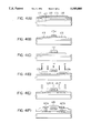
- FIGS. 1(A) through 1(C) The invention is conceptually illustrated in FIGS. 1(A) through 1(C).
- a base insulating film 2 is deposited on a substrate 1, an island-shaped silicon region 3 is formed, and a gate insulating film 4, a lower-layer aluminum film 5 (over 99.5% pure), and an upper-layer aluminum film 6 (containing over 0.5% and preferably over 2% silicon) are deposited covering the island-shaped silicon region 3.
- FIGS. 1(A) A base insulating film 2 is deposited on a substrate 1
- an island-shaped silicon region 3 is formed, and a gate insulating film 4, a lower-layer aluminum film 5 (over 99.5% pure), and an upper-layer aluminum film 6 (containing over 0.5% and preferably over 2% silicon) are deposited covering the island-shaped silicon region 3.
- a film 7 of amorphous silicon or having amorphous silicon as its main component may be formed by sputtering or CVD or the like as an anti-reflection film.
- a second aspect of the invention comprises etching the kind of residue deposits discussed above using a mixture solution (a mixed acid) of hydrofluoric acid, nitric acid and acetic acid.
- a mixture solution a mixed acid
- hydrofluoric acid (HF) 1, the nitric acid (HNO 3 ) is made 100 to 400, and preferably 180 to 220, and the acetic acid (CH 3 COOH) is made 100 to 300, and preferably 130 to 170.
- the etching depth of the aluminum at this time was 20 to 60 ⁇ and the etching depth of the silicon oxide was 80 to 240 ⁇ , and compared to the usual thickness of 2000 to 10,000 ⁇ of the aluminum film and the usual thickness 1000 to 2000 ⁇ of the silicon oxide film serving as the gate insulation film almost no substantial adverse effect resulting from this degree of etching was observed.
- a third aspect of the invention comprises forming an interlayer insulating film and contact holes before performing laser annealing and performing laser annealing thereafter. In this way, because in the contact hole regions no silicon oxide exists to undergo a reaction, no nonstoichiometric silicon oxide film of the kind mentioned above is formed. After that, reliable contacts are formed by forming metal electrodes in these contact holes.
- a fourth aspect of the invention makes it possible for abnormal growth in oxidization steps and heating steps of materials having IIIa group elements as their main components to be prevented, by adding to materials having IIIa group elements as their main components a IIIb group element.
- the IIIb group elements referred to here are Sc, Y, lanthanoids and actinoids, and the IIIa group elements are B, Al, Ga, In, Tl.
- this amount is made less than 0.1 wt %, or still less preferably is made less than 0.05 wt %, the heat-resistance is not satisfactory and hillocks appear within 1 hour at 350° C.
- wet etching and dry etching can be used in the same way as has been done conventionally.
- dry etching when depending on the etching conditions the added elements (scandium, etc) remain as residue, and particularly when the amount of this residue is over 0.40 wt % or even 0.25 wt %, some residue may remain on the surface etched by the dry etching; however, this residue can be removed by washing with pure water.
- Sc has an ionization rate higher than that of aluminum, and in the anodic oxidation process does not impede the oxidation of aluminum. Therefore, a dense anodic oxide layer can be formed. And, because the effect of suppressing the movement of aluminum at the atomic level is strong, the formation of hillocks by heating or by the anodic oxidation process can be suppressed. Also, because the anodic oxide layer is dense and its surface is smooth, and because there is no surface irregularity at the interface between the anodic oxide layer and the aluminum film either, the light reflectivity is excellent and the laser-resistance is increased.
- FIGS. 1(A) through 1(C) illustrate an example of the structure of the gate of a TFT according to the present invention
- FIGS. 2(A) and 2(B) illustrate an example of the structure of the gate of a conventional TFT
- FIGS. 3(A) through 3(E) are cross-sectional views illustrating a manufacturing process according to a first preferred embodiment of the invention
- FIGS. 4(A) through 4(F) are cross-sectional views illustrating a manufacturing process according to a third preferred embodiment of the invention.
- FIGS. 5(A) through 5(F) are cross-sectional views illustrating a manufacturing process according to a fourth preferred embodiment of the invention.
- FIGS. 6(A) through 6(E) are cross-sectional views illustrating a TFT manufacturing process according to a fifth preferred embodiment of the invention.
- FIGS. 7(A) through 7(E) are cross-sectional views illustrating a conventional TFT manufacturing process
- FIG. 8 is a view illustrating the structure of a TFT having offset gate regions
- FIGS. 9(A) through 9(D) are cross-sectional views illustrating a manufacturing process according to a sixth preferred embodiment of the invention.
- FIGS. 10(A) through 10(E) are cross-sectional views illustrating a manufacturing process according to a seventh preferred embodiment of the invention.
- FIGS. 11(A) and 11(B) are photographs showing the state of a thin film formed by anodic oxidation.
- FIGS. 12(A) through 12(E) are cross-sectional views illustrating a manufacturing process according to a second preferred embodiment of the invention.
- FIGS. 3(A) through 3(E) A manufacturing process according to a first preferred embodiment of the invention is illustrated in FIGS. 3(A) through 3(E).
- a silicon oxide base film 32 of thickness 2000 ⁇ was formed on a substrate (Corning 7059) 31 by sputtering.
- This amorphous silicon film was then crystallized by annealing in a nitrogen atmosphere at 600° C. for 48 hours.
- the silicon film was patterned, an island-shaped silicon region 33 was formed, and by sputtering a silicon oxide film 34 of thickness 1000 ⁇ was deposited as a gate insulating film.
- silicon oxide was used as a target
- the substrate temperature during sputtering was 200° to 400° C., for example 250° C.
- the purity of the aluminum was over 99.9%. It is desirable that this silicon oxide film and this aluminum film be formed in consecutive steps.
- the first and second aluminum films were then patterned to form a gate electrode (consisting of a first aluminum layer 35 and a second aluminum layer 36). (FIG. 3(A))
- anodic oxide (aluminum oxide) 37 was caused to grow on the surface of the gate electrode.
- an impurity phosphorus
- Phosphine PH 3
- the dose quantity was 1 ⁇ 10 15 to 8 ⁇ 10 15 cm -2 , for example 2 ⁇ 10 15 cm -2 .
- N-type impurity regions 38a, 38b were created.
- laser annealing was carried out by irradiation with laser light.
- a KrF excimer laser (wavelength 248 nm, pulse width 20 nsec) was used as the laser, but other lasers, for example an XeF excimer laser (wavelength 353 nm), an XeCl excimer laser (wavelength 308 nm), or an ArF excimer laser (wavelength 193 nm), may be used.
- the laser energy density was made 200 to 500 mJ/cm 2 , for example 250 mJ/cm 2 , and 2 to 10 shots, for example 2 shots, of irradiation were carried out per location.
- the substrate was heated to 100° to 450° C., for example 250° C. In this way, the impurity was activated. (FIG. 3(D))
- a silicon oxide film 39 of thickness of 6000 ⁇ was then formed as an interlayer insulator by plasma CVD, contact holes were formed in this, and TFT source region and drain region electrodes/leads 40a, 40b were formed using a metallic material, for example a multilayer film of titanium nitride and aluminum. Finally, annealing was carried out in hydrogen at one atmosphere and at 350° C. for 30 minutes. By the process described above a TFT was completed. (FIG. 3(E))
- FIGS. 12(A) through 12(E) A manufacturing process according to a second preferred embodiment of the invention is illustrated in FIGS. 12(A) through 12(E).
- a silicon oxide base film 42 of thickness of 2000 ⁇ was formed on a substrate (Corning 7059) 41 by sputtering.
- This silicon film was patterned to form an island-shaped silicon film 43.
- the silicon region was crystallized.
- a KrF excimer laser (wavelength 248 nm) was used as the laser, the laser energy density was made 200 to 500 mJ/cm 2 , for example 350 mJ/cm 2 , and 2 to 10 shots, for example 2 shots, of irradiation were carried out per location.
- the substrate was heated to 100° to 450° C., for example 350° C.
- a silicon oxide film 44 of thickness 1000 ⁇ was formed by plasma CVD as a gate insulating film of a crystal silicon TFT.
- trichloroethylene C 2 HCl 3
- 400 SCCM of oxygen was fed into a chamber, plasma was generated with the substrate temperature at 300° C. and the total pressure at 5 Pa and with an RF power of 150 W, and this state was maintained for 10 minutes.
- the purity of the aluminum was over 99.9%.
- an amorphous silicon film of thickness 100 to 2000 ⁇ , for example 200 ⁇ was then deposited. This multilayer film was then patterned to form a TFT gate electrode 45. An anti-reflection film 46 remained on the top of the gate electrode. Because of the presence of the anti-reflection film, it was possible for example to conduct fine patterning of even less than 7 ⁇ m with good precision. (FIG. 12(A))
- this gate electrode 45 and the anti-reflection film 46 were anodically oxidized to form an oxide layer (aluminum oxide and silicon oxide) 47 on the surface.
- the anodic oxidation was carried out in a 1 to 5% solution of tartaric acid in ethylene glycol.
- the anti-reflection film 46 was almost completely oxidized.
- an impurity phosphorus
- the acceleration voltage was made 80 kV, and the dose quantity was made 2 ⁇ 10 15 cm -2 .
- N-type impurity regions 48a, 48b were created.
- the impurity was activated by laser annealing.
- a KrF excimer laser (wavelength 248 nm, pulse width 20 nsec) was used as the laser, and the laser energy density was made 200 to 500 mJ/cm 2 , for example 250 mJ/cm 2 , and 2 to 10 shots, for example 2 shots, of irradiation were carried out per location.
- the substrate was heated to 100° to 450° C., for example 250° C. In this way, the impurity was activated. (FIG. 12(D))
- a silicon oxide film 49 of thickness 2000 ⁇ was formed as an interlayer insulator by plasma CVD with TEOS as a raw material, contact holes were formed in this, and source and drain electrodes/leads 50a, 50b were formed using a metal material, for example a multilayer film of titanium nitride and aluminum.
- a metal material for example a multilayer film of titanium nitride and aluminum.
- the electric field effect mobility of the thin film transistors produced was such that with a gate voltage of 10 V and 70 to 100 cm 2 /Vs the threshold value was 2.5 to 4.0 V, and the leak current when a voltage of -20 V was impressed on the gate was less than 10 -13 A.
- FIGS. 4(A) through 4(F) A manufacturing process according to a third preferred embodiment of the invention is illustrated in FIGS. 4(A) through 4(F).
- a silicon oxide base film 412 of thickness 2000 ⁇ was formed on a substrate (Corning 7059) 411 by sputtering.
- This amorphous silicon film was then crystallized by annealing in a nitrogen atmosphere at 600° C. for 48 hours.
- the silicon film was patterned, an island-shaped silicon region 413 was formed, and by sputtering a silicon oxide film 414 of thickness 1000 ⁇ was deposited as a gate insulating film.
- silicon oxide was used as a target
- the substrate temperature during sputtering was 200° to 400° C., for example 250° C.
- the aluminum film 415 was then etched with a mixed acid having phosphoric acid as its main component, and a gate electrode 415a was formed. As a result of this etching process a deposit 416 whose main component was silicon was left on top of the silicon oxide layer 414. (FIG. 4(B))
- the deposit was etched by the substrate being immersed for 30 seconds in an acid mixture of constituent ratio hydrofluoric acid 1, nitric acid 200 and acetic acid 150.
- the substrate was then immersed in a solution of tartaric acid in ethylene glycol (1 to 5%, neutralized with ammonia), a current was passed through the gate electrode, and an anodic oxide layer (aluminum oxide) 417 was thereby caused to grow on the surface of the gate electrode.
- anodic oxide layer aluminum oxide
- 1000 to 5000 ⁇ , and especially 2000 to 3000 ⁇ was desirable. In this example the thickness was made 2500 ⁇ . (FIG. 4(C))
- an impurity phosphorus
- Phosphine PH 3
- the dose quantity was 1 ⁇ 10 15 to 8 ⁇ 10 15 cm -2 , for example 2 ⁇ 10 15 cm -2 .
- N-type impurity regions 418a, 418b were created.
- laser annealing was carried out by irradiation with laser light.
- a KrF excimer laser (wavelength 248 nm, pulse width 20 nsec) was used as the laser, but other lasers, for example an XeF excimer laser (wavelength 353 nm), an XeCl excimer laser (wavelength 308 nm), or an ArF excimer laser (wavelength 193 nm), may be used.
- the laser energy density was made 200 to 500 mJ/cm 2 , for example 250 mJ/cm 2 , and 2 to 10 shots for example 2 shots, of irradiation were carried out per location.
- the substrate was heated to 100° to 450° C., for example 250° C. In this way, the impurity was activated. (FIG. 4(E))
- a silicon oxide film 419 of thickness 6000 ⁇ was then formed as an interlayer insulator by plasma CVD, contact holes were formed in this, and TFT source region and drain region electrodes/leads 420a, 420b were formed using a metallic material, for example a multilayer film of titanium nitride and aluminum. Finally, annealing was carried out in hydrogen at one atmosphere and at 350° C. for 30 minutes. By the process described above a TFT was completed. (FIG. 4(F))
- FIGS. 5(A) through 5(F) A manufacturing process according to a fourth preferred embodiment of the invention is illustrated in FIGS. 5(A) through 5(F).
- a silicon oxide base film 522 of thickness 2000 ⁇ was formed on a substrate (Corning 7059) 521 by sputtering.
- an intrinsic (I-type) amorphous silicon film of thickness 200 to 1500 ⁇ , for example 500 ⁇ was deposited.
- This silicon film was patterned to form an island-shaped silicon film 523.
- the silicon region was crystallized.
- a KrF excimer laser (wavelength 248 nm) was used as the laser, the laser energy density was made 200 to 500 mJ/cm 2 , for example 350 mJ/cm 2 , and 2 to 10 shots, for example 2 shots, of irradiation were carried out per location.
- the substrate was heated to 100° to 450° C., for example 350° C.
- a silicon oxide film 524 of thickness 1000 ⁇ was formed by plasma CVD as a gate insulating film of a crystal silicon TFT.
- trichloroethylene C 2 HCl 3
- 400 SCCM of oxygen was fed into a chamber, plasma was generated with the substrate temperature at 300° C. and the total pressure at 5 Pa and with an RF power of 150 W, and this state was maintained for 10 minutes.
- an aluminum film 525 containing 0.5 to 3% silicon, for example 2% silicon was deposited to a thickness of 1000 to 10,000 ⁇ , for example 5000 ⁇ .
- the aluminum film 525 was then etched with a mixed acid having phosphoric acid as its main component, and a gate electrode 525a was formed. As a result of this etching process a deposit 526 whose main component was silicon was left on top of the silicon oxide layer 524. (FIG. 5(B))
- the deposit was etched by the substrate being immersed for 30 seconds in an acid mixture of constituent ratio hydrofluoric acid 1, nitric acid 200 and acetic acid 150.
- the substrate was then immersed in a solution of tartaric acid in ethylene glycol (1 to 5%, neutralized with ammonia), a current was passed through the gate electrode, and an anodic oxide layer (aluminum oxide) 527 was thereby caused to grow on the surface of the gate electrode.
- anodic oxide layer aluminum oxide
- 1000 to 5000 ⁇ , and especially 2000 to 3000 ⁇ was desirable. In this example the thickness was made 2500 ⁇ . (FIG. 5(C))
- an impurity phosphorus
- Phosphine PH 3
- the dose quantity was 1 ⁇ 10 15 to 8 ⁇ 10 15 cm -2 , for example 2 ⁇ 10 15 cm -2 .
- N-type impurity regions 528a, 528b were created.
- a silicon oxide film 529 of thickness 6000 ⁇ was then formed as an interlayer insulator by plasma CVD, contact holes were formed in this, and TFT source region and drain region electrodes/leads 530a, 530b were formed using a metallic material, for example a multilayer film of titanium nitride and aluminum. Finally, annealing was carried out in hydrogen at one atmosphere and at 350° C. for 30 minutes. By the process described above a TFT was completed. (FIG. 5(F))
- the electric field effect mobility of the thin film transistors produced was such that with a gate voltage of 10 V and 70 to 100 cm 2 /Vs the threshold value was 2.5 to 4.0 V, and the leak current when a voltage of -20 V was impressed on the gate was less than 10 -13 A.
- FIGS. 6(A) through 6(E) A manufacturing process according to a fifth preferred embodiment of the invention is illustrated in FIGS. 6(A) through 6(E).
- a silicon oxide base film 612 of thickness 2000 ⁇ was formed on a substrate (Corning 7059) 611 by sputtering.
- This amorphous silicon film was then crystallized by annealing in a nitrogen atmosphere at 600° C. for 48 hours.
- This step may be carried out using laser annealing.
- the laser any of the excimer lasers can be used.
- the laser energy density should be made 200 to 500 mJ/cm 2 , for example 350 mJ/cm 2 ; 2 to 10 shots of irradiation should be carried out per location, and the substrate should be heated to 100° to 450° C. for the laser irradiation.
- the silicon film was patterned, an island-shaped silicon region 613 was formed, and by sputtering a silicon oxide film 614 of thickness 1000 ⁇ was deposited as a gate insulating film.
- silicon oxide was used as a target
- the substrate temperature during sputtering was 200° to 400° C., for example 250° C.
- aluminum instead of aluminum, other metals and semiconductor materials such as silicon, titanium, tantalum, molybdenum or tungsten, or silicides of these, may be used. Also, this does not have to be a single-layer film, and may instead be a multilayer film consisting of different films superposed. (FIG. 6(A))
- the substrate was then immersed in a solution of tartaric acid in ethylene glycol (1 to 5%, neutralized with ammonia), a current was passed through the gate electrode, and an anodic oxide (aluminum oxide) layer 616 was thereby caused to grow on the surface of the gate electrode.
- anodic oxide aluminum oxide
- an impurity phosphorus
- Phosphine PH 3
- the dose quantity was 1 ⁇ 10 15 to 8 ⁇ 10 15 cm -2 , for example 2 ⁇ 10 15 cm -2 .
- N-type impurity regions 617a, 617b were created.
- a silicon oxide film 618 of thickness 6000 ⁇ was then formed as an interlayer insulator by plasma CVD, and contact holes 619a, 619b were formed in this silicon oxide film 618.
- laser annealing was carried out by irradiation with laser light.
- a KrF excimer laser (wavelength 248 nm, pulse width 20 nsec) was used as the laser, but other lasers, for example an XeF excimer laser (wavelength 353 nm), an XeCl excimer laser (wavelength 308 nm), or an ArF excimer laser (wavelength 193 nm) may be used.
- it is necessary that the laser light satisfactorily permeate the interlayer insulator 618.
- the laser energy density was made 200 to 500 mJ/cm 2 , for example 250 mJ/cm 2 , and 2 to 10 shots, for example 2 shots, of irradiation were carried out per location.
- the substrate was heated to 100° to 450° C., for example 250° C. In this way, the impurity was activated. (FIG. 6(D))
- TFT source region and drain region electrodes/leads 620a, 620b were formed using a metallic material, for example a multilayer film of titanium nitride and aluminum. Removing the natural oxide film of silicon which had formed on the contact portions by cleaning the substrate with dilute hydrofluoric acid before depositing the metallic material made it possible to form more complete contacts. Finally, annealing was performed in hydrogen at 1 atmosphere and at 350° C. for 30 minutes. By the above process, a thin film transistor was completed. (FIG. 6(E))
- This preferred embodiment is an example of the creation of a circuit, shown in FIGS. 9(A) through 9(D), using a crystalline silicon film formed on a glass substrate 201, wherein a P-channel TFT (a PTFT) and an N-channel TFT (an NTFT) are combined complimentarily.
- a PTFT P-channel TFT
- an NTFT N-channel TFT
- FIGS. 9(A) through 9(D) A manufacturing process according to this sixth preferred embodiment of the invention is illustrated in FIGS. 9(A) through 9(D).
- a silicon oxide base film 202 of thickness 2000 ⁇ was formed on a substrate (Corning 7059) 201 by sputtering. If before the base film is formed the substrate is annealed at a temperature higher than its distortion temperature and then gradually cooled at 0.1° to 1.0° C./minute to below the distortion temperature, shrinkage of the substrate during subsequent steps (including for example infrared light irradiation) accompanying temperature increases is slight and mask alignment becomes easy.
- the substrate be annealed at 620° to 660° C. for 1 to 4 hours, gradually cooled at 0.1° to 1.0° C./minute, preferably 0.03° to 0.3° C./minute, and taken out when its temperature has fallen to 400° to 500° C.
- the silicon film was patterned to form a TFT island-shaped active layer 205.
- the size of the active layer 205 is decided in consideration of the channel length and the channel width of the TFT. In small TFTs this was 50 ⁇ m ⁇ 20 ⁇ m, and in large TFTs this was 100 ⁇ m ⁇ 1000 ⁇ m. Many such active layers were formed on the substrate.
- irradiation with infrared light having a peak at 0.6 to 4 ⁇ m, in this example 0.8 to 1.4 ⁇ m was carried out for 30 to 180 seconds to promote the crystallization of the active layer.
- the temperature was made 800° to 1300° C., typically 900° to 1200° C., for example 1100° C.
- the irradiation was performed in an H 2 atmosphere. In this step, because the active layer is heated selectively, it is possible to minimize the application of heat to the glass substrate. The step is extremely effective in reducing faults and dangling bonds in the silicon film. (FIG. 9(B))
- a halogen lamp was used as the infrared light source.
- the strength of the visible/near-infrared light was adjusted so that the temperature on a monitor single-crystal silicon wafer was 800° to 1300° C. and typically between 900° and 1200° C. Specifically, the temperature of a thermocouple inlaid in the silicon wafer was monitored and this was fed back to the infrared light source. The temperature of the silicon surface on the glass substrate was estimated to be about 2/3 of this.
- a silicon oxide or silicon nitride film be formed on the surface as a protective film. This is in order to improve the state of the surface of the silicon film 205.
- the irradiation was performed in an H 2 atmosphere; however, 0.1 to 10 vol % HCl, or hydrohalogen or compounds of fluorine or chlorine, bromine, etc, may be mixed into the H 2 atmosphere.
- the crystallized silicon film is heated selectively, it is possible to minimize the application of heat to the glass substrate.
- the step is extremely effective in reducing faults and dangling bonds in the silicon film.
- Performing hydrogen annealing at 200° to 500° C., typically 350° C., after the RTA step is finished is also is effective in reducing faults.
- the same effects can be obtained by carrying out doping of a quantity of 1 ⁇ 10 13 to 1 ⁇ 10 15 cm -2 hydrogen ions and then performing heat treatment at 200° to 300° C.
- a silicon oxide film 206 of thickness 1000 ⁇ was formed by plasma CVD as a gate insulating layer.
- TEOS tetra-ethoxy-silane (Si(OC 2 H 5 ) 4 ) and oxygen were used, and the substrate temperature during film-forming was made 300° to 550° C., for example 400° C.
- this silicon film 206 was formed to serve as a gate insulating layer, light-annealing with visible/near-infrared rays was again carried out, under the same conditions as those used for the RTA process described above and in an atmosphere of N 2 O or NH 3 .
- this annealing it was possible to eliminate levels mainly at and near the interface between the silicon oxide film 206 and the silicon film 205. This is extremely useful for insulated gate field effect semiconductor devices, because in these devices the characteristics of the interface between the gate insulating film and the channel-forming region are extremely important.
- this aluminum is contained 0.2 wt % Sc.
- rare earth elements of periodic table group IIIa can be used.
- the contained quantity can be made 0.05 to 0.40 wt %, preferably 0.1 to 0.25 wt %.
- the aluminum film was then patterned and etched to form gate electrodes 207, 209.
- dry etching was used.
- the surfaces of these aluminum electrodes were anodically oxidized, and an oxide layer 208, 210 was formed surface of each electrode.
- This anodic oxidization was carried out in a 1 to 5% solution of tartaric acid in ethylene glycol. Anodic oxidation was brought about by raising the voltage to 150 V at 4 V/min.
- the thickness of the oxide layers 208, 210 obtained was 2000 ⁇ . Because the thickness of these oxides 208 and 210 creates offset gate regions in the subsequent ion doping step, the length of the offset gate regions can be set in the anodic oxidation step mentioned above.
- ion doping also called plasma doping
- the gate electrode parts i.e. the gate electrode 207 and the oxide layer 208 on the periphery thereof, and the gate electrode 209 and the oxide layer 210 on the periphery thereof
- impurities imparting P and N conductivity types were added to the silicon film 205 in a self-aligning manner.
- the doping gas phosphine (PH 3 ) and diborane (B 2 H 6 ) were used; with the former the accelerating voltage was made 60 to 90 kV, for example 80 kV, and with the latter the accelerating voltage was made 40 to 80 kV, for example 65 kV.
- the doping quantity was made 1 ⁇ 10 14 to 1 ⁇ 10 15 cm -2 , for example 2 ⁇ 10 15 cm -2 of phosphorus and 5 ⁇ 10 15 of boron.
- the respective elements were selectively doped.
- N-type impurity regions 214 and 216, and P-type impurity regions 211 and 213 were formed, and a P-channel TFT (PTFT) region and an N-channel TFT (NTFT) region could be created.
- PTFT P-channel TFT
- NTFT N-channel TFT
- annealing by irradiation with laser light was carried out.
- a KrF excimer laser (wavelength 248 nm, pulse width 20 nsec) was used as the laser, but other lasers may be used.
- the laser light irradiation conditions were that the laser energy density was made 200 to 400 mJ/cm 2 , for example 250 mJ/cm 2 , and 2 to 10 shots, for example 2 shots, of irradiation were carried out per location.
- the substrate may be heated to 200° to 450° C. for this laser light irradiation to increase the effect of the irradiation. (FIG. 9(C))
- This step may alternatively be performed by a method using lamp annealing with visible/near-infrared light.
- Visible/near-infrared light is easily absorbed by crystallized silicon and by noncrystalline silicon to which phosphorus or boron has been added to a concentration of 10 17 to 10 21 cm -3 , and annealing of effectiveness comparable to that of thermal annealing can be carried out.
- phosphorus or boron has been added, because of the dispersion of this impurity, even near-infrared light is well absorbed. This can be easily conjectured from the fact that the film is black in color even to the naked eye.
- the method can be said to be ideal for processes in which shrinkage of the glass substrate is a problem.
- a silicon oxide film 217 of thickness 6000 ⁇ was then formed as an interlayer insulator by plasma CVD.
- Polyimide or a 2-layer film of silicon oxide and polyimide can alternatively be used as this interlayer insulator.
- Contact holes were formed, and TFT electrodes/leads 218, 220, 219 were formed using a metallic material, for example a multilayer film of titanium nitride and aluminum.
- annealing was carried out in hydrogen at one atmosphere and at 350° C. for 30 minutes, and a semiconductor circuit comprising complimentarily structured TFTs was completed. (FIG. 9(D))
- the circuit described above is a structure in which a PTFT and an NTFT are provided complimentarily; however, it is also possible in the above process to make two TFTs simultaneously and then cut them apart down the middle, thereby producing two independent TFTs at one time.
- FIGS. 10(A) through 10(E) A manufacturing process according to a seventh preferred embodiment of the invention is illustrated in FIGS. 10(A) through 10(E).
- a base film 302 comprising aluminum nitride of thickness 2000 ⁇ and on top of that a silicon oxide film of thickness 200 ⁇ was formed on a substrate (Corning 7059) 301 by sputtering.
- sputtering a silicon oxide film of thickness 200 ⁇ was deposited on the amorphous silicon film.
- This amorphous silicon film was then crystallized by annealing in a nitrogen atmosphere at 600° C. for 48 hours. After annealing, the silicon film was patterned to form an island-shaped silicon region 303, and then by sputtering a silicon film 304 of thickness 1000 ⁇ was deposited as a gate insulating film.
- silicon oxide was used as a target
- the substrate temperature during sputtering was 200° to 400° C., for example 250° C.
- 0.05 to 0.4 wt %, for example 0.15 wt % scandium (Sc) was added.
- a photoresist having good resistance to pressure such as Shipley Co.'s AZ1350, of thickness approximately 1 ⁇ m, was formed by spin-coating.
- a gate electrode 305 was patterned. For the etching, wet etching was employed, and a mixture of phosphoric acid and nitric acid was used as the etchant.
- a photoresist mask 306 was left on the top of the gate electrode.
- a photosensitive polyimide such as Toray Co.'s UR3800 (Photoneece) can be used to obtain a similar structure. (FIG. 10(A))
- a porous anodic oxide 307 of thickness of from 4000 to 10,000 ⁇ (1 ⁇ m), and in this example approximately 5000 ⁇ , could be formed on the side surface of the gate electrode with a precision of ⁇ 200 ⁇ .
- anodic oxidation may be performed in 8% oxalic acid solution at 30 to 40 V. Because the mask material was still in place on the upper surface of the gate electrode, almost no anodic oxidation proceeded there. (FIG. 10(B))
- an impurity phosphorus
- Phosphine PH 3
- the dose quantity was 1 ⁇ 10 14 to 8 ⁇ 10 15 cm -2 , for example 2 ⁇ 10 15 cm -2 .
- N-type impurity regions 309 were created.
- a KrF excimer laser (wavelength 248 nm, pulse width 30 nsec) was used as the laser, but other lasers, for example an XeCl excimer laser (wavelength 308 nm), an ArF excimer laser (wavelength 193 nm), or an XeF excimer laser (wavelength 353 nm), may be used.
- the laser energy density was made 200 to 400 mJ/cm 2 , for example 250 mJ/cm 2 , and 2 to 10 shots, for example 2 shots, of irradiation were carried out.
- the substrate was heated to 200° to 300° C., for example 250° C. In this way, the impurity regions 309 were activated.
- the porous anodic oxide 307 is still present, but this oxide 307 may be removed hereafter. Also, the gate insulating film beneath the gate electrode and the gate insulating film 304 below that may be removed. When this is done, the porous anodic oxide 307 does not capture electric charges and cause instability.
- a silicon oxide film 310 of thickness 6000 ⁇ was then formed as an interlayer insulator by plasma CVD, contact holes were formed in this, and TFT source region and drain region electrodes/leads 311 were formed using a metallic material, for example a multilayer film of titanium nitride and aluminum. Finally, annealing was carried out in hydrogen at one atmosphere and at 350° C. for 30 minutes. By the process described above a TFT was completed. (FIG. 10(E))
- the TFT offset (the distance between the edges of the gate electrode 305 and the source/drain regions 307) was as much as 5000 ⁇ (porous anodic oxide 3000 ⁇ +non-porous anodic oxide 1000 ⁇ ), and as a result the leak current (I OFF ) was kept extremely low.
- the TFT is suitable for use for example as a pixel transistor in an active matrix-type liquid crystal display.
- This preferred embodiment is a comparison example comparing a case wherein by an anodic oxidation step an anodic oxide layer is formed to a thickness of 2000 ⁇ on the surface of an aluminum film to which 0.2 wt % Si has been added with a case wherein by an anodic oxidation step under the same conditions an anodic oxide layer is formed on the surface of an aluminum film to which 0.2 wt % Sc has been added.
- the thickness of the aluminum film was 6000 ⁇ , and the film was formed by sputtering.
- the anodic oxidation step was the same as that described in the sixth preferred embodiment: by immersing the aluminum film in a 1 to 5% solution of tartaric acid in ethylene glycol and increasing the voltage at 4 V/min to 150 V, an oxide film of thickness 2000 ⁇ was formed.
- FIG. 11(A) shows the state of a film whose main component is aluminum, formed in an island-shape, and an oxide layer formed thereon in the anodic oxide step.
- FIG. 11(B) is an electron microscope photograph taken in the case wherein Sc was added to the aluminum. From FIG. 11(B) it can be seen that the oxide layer is dense and that there is no trace of any abnormal growth in the surface.
- a uniform anodic oxide layer can be formed.
- the heat-resistance can be increased.
- the laser-resistance can be increased.
- the TFT characteristics can be made uniform.
Abstract
A thin film transistor according to this invention has a gate electrode comprising a lower layer of aluminum of a high purity of over 99.5% and an upper layer of aluminum containing over 0.5% silicon. Alternatively, it has a gate electrode made by adding a IIIa group element to a IIIb group element. Residues produced by the etching of the silicon-containing aluminum gate electrode are etched with a mixture solution of hydrofluoric acid, nitric acid and acetic acid. After contact holes have been formed in an interlayer insulating film, laser annealing is carried out, and metal electrodes are formed in the contact holes thereafter.
Description
This invention relates to a method for producing a thin film transistor (TFT) having a noncrystal semiconductor thin film. A thin film transistor manufactured according to this invention may be formed on an insulating substrate such as glass or on a semiconductor substrate such as monocrystalline silicon.
Recently, research has been being carried out on insulated gate-type semiconductor devices having thin film-form active layers (also called active regions) on insulating substrates. In particular, thin film insulated gate transistors, or so-called thin film transistors (TFTs), have been being researched intensively. These are divided up according to the material and crystal state of the semiconductor used into types such as amorphous silicon TFTs and crystalline silicon TFTs.
Crystalline semiconductors have greater electric field mobility than amorphous semiconductors and therefore are capable of operating at high speeds. Also, with crystalline silicon, because not only NMOS TFTs but also PMOS TFTs can be similarly obtained, it is possible to create CMOS circuits. Because of this, particularly TFTs made using crystal silicon have recently been being heavily researched.
In crystal semiconductors, as a gate electrode material, the use of aluminum has been being researched because it has the merit that its sheet resistance is low. However, with pure aluminum, in heat treatment at over 100° C., hillocks have formed. These hillocks have not been so much of a problem in devices of channel length over 10 μm, but in devices of lower channel length, and typically in 2 to 10 μm devices, they have led to irremediable defects.
Because of this, a material made by adding over 0.5% and preferably over 2% silicon to aluminum to suppress the occurrence of hillocks has usually been used. The method by which this kind of gate electrode is formed is shown in FIGS. 2(A) and 2(B). On a substrate 11, a base insulating film 12 is deposited, an island-shaped silicon region 13 is formed, a gate insulating film 14 is deposited covering this, and then an aluminum film 15 is deposited by vacuum deposition or by sputtering. (FIG. 2(A))
Patterning is then carried out by a known photolithography method, the aluminum film 15 is etched, and a gate electrode 15a is formed. For the etching, from the mass-production viewpoint, wet etching using an acid such as phosphoric acid has been used. However, with this kind of etching, a residue deposit such as that shown by reference numeral 16 in FIG. 2(B) has been observed. This deposit has silicon as its main component and is silicon which has remained without being etched, or is a product of coagulation of aluminum silicide, in the etching step. (FIG. 2(B))
To remove this deposit 16, treatment with an acid containing hydrofluoric acid has been necessary, but this treatment has inflicted damage on the gate insulating film 14 (usually silicon oxide) or the activate region (usually silicon) below. That is, the gate insulating film or the active region has undergone significant etching, and, as a result, in cases such as when the gate electrode is later anodically oxidized, holes have opened up between the anodic oxide of the gate electrode and the gate insulating film and reliability has been reduced. Consequently, the selective removal of this kind of residue only has been being sought. This invention was devised in view of this problem and provides a method of selectively etching deposits while maintaining mass-production.
TFTs can be used as pixel electrode switching elements in active matrix liquid crystal displays, or as driving elements in peripheral driver circuits. They can also be used for image sensors and for other integrated circuits.
As a TFT structure, the structure illustrated in FIG. 8 has been proposed. The TFT shown in FIG. 8 has an active layer comprising a noncrystalline or crystalline silicon thin film formed on a glass substrate 111 and having a source 112, a drain 114 and a channel 113, a silicon oxide film constituting a gate insulating layer 116, a gate electrode 117 whose main component is aluminum and a silicon oxide layer 118 on the periphery thereof, an interlayer insulating film 119, a source electrode 101 and a drain electrode 102.
Here, crystalline silicon film refers to a film such as microcrystal silicon film, polycrystalline silicon film or semi-amorphous silicon film which has silicon containing an ordered structure as its main component.
What is important in the structure illustrated in FIG. 8 is that the thickness of the oxide layer 118 formed on the periphery of the gate electrode 117 is used to form offset gate regions 115. In the structure shown in FIG. 8, the source 112 and the drain 114 are formed by ion implantation or by ion doping, and in this the gate electrode 117 and the oxide layer 118 thereon serve as a mask.
As a result, as shown by the reference numeral 115, on both sides of the portion 113 which functions as a channel, regions which function neither as a channel nor as a source/drain, or which function as both, are formed. These regions 115 are called offset gate regions and serve the purpose of acting to alleviate electrical field concentrations between the channel and the source and between the channel and the drain. By providing these offset gate regions it is possible to obtain benefits such as reductions in the OFF current during reverse bias application and increases in the ON-OFF ratio.
Reversely, it is possible to some extent to control the TFT characteristics by way of the width 103 of these offset regions 115 (which thickness is determined by the thickness of the oxide layer 118). Accordingly, when the thickness of the oxide layer 118 cannot be well controlled, variations occur in the characteristics of the TFTs.
The oxide layer 118 is formed after the formation of the aluminum gate electrode 117 by for example immersing the substrate in a 3% solution of tartaric acid in ethylene glycol (pH-adjusted to neutral with ammonia) and increasing a voltage across the gate electrode 117 at 1 to 5 V/min, for example 4 V/min, to 120 V.
In general, the thickness of the oxide layer 118 is set to approximately 1000 to 2000 Å. This results in the thickness 103 of the offset gate regions 115 being 500 Å to 1 μm, for example 1000 to 2000 Å. Of course, the thickness of the offset gate regions 115 is decided according to the requirements of the application. However, in the TFT production process heating steps and steps involving irradiation with flash lamp light or laser light are necessary, and in such steps it is necessary that the oxide layer 118 be durable (laser-resistant and heat-resistant).
According to numerous experiments carried out by the present inventors, when pure aluminum is used for the gate electrode there has been the problem that in the anodic oxidation process abnormal growth of the aluminum occurs (hillocks).
Also, it was found that in structures in which an anodic oxide is formed on the surface of an aluminum film obtained in this way, and especially when the anodic oxide film is thin, there is the problem that the resistance to irradiation with strong light such as laser light (the laser-resistance) is poor, and there is no resistance to heat. (That is, hillocks form and the anodic oxide layer breaks up. Especially in heat treatment at over 350° C., hillock formation was marked.)
A cause of the above problem may be that when given a large amount of energy aluminum atoms readily move around at the atomic level. A method of solving this problem might be to add a small quantity of a material whose melting point is higher than that of aluminum and thereby suppress the movement of aluminum at the atomic level. One technique might therefore be to add Si or Pd to the aluminum. The addition of this kind of element suppresses the formation of hillocks and increases the resistance to heat.
However, there is the problem that because the ionization rates of Si and Pd and the like are low compared to that of aluminum, in the anodic oxidation process the anodic oxide layer cannot be made thick. Also, because the oxidation rates of Si, which is a periodic table group IVb element, and Pd, which is a periodic table group VIII element, are lower than the rates at which aluminum oxidizes, there has been the problem that oxidation does not proceed uniformly, the thickness of the oxide layer is not uniform, and it is not possible to form a dense oxide layer (see Eighth Preferred Embodiment). As a result of this, the heat-resistance is actually reduced. Also, when this kind of material is used to make a TFT of the kind shown in FIG. 8, because the thickness of the oxide layer 118 differs from place to place there is the problem that the width of the offset regions 115 also varies.
Crystal silicon is usually obtained by annealing for a long period of time at a temperature of over 600° C., and heat treatment at a similar temperature has also been required to activate the doping impurity in crystal silicon which has been doped by a method such as ion implantation or ion doping. However, because this kind of high-temperature heat treatment reduces the freedom with which the substrate and structural materials of the TFT can be selected, treatment at low temperatures has been being sought.
As a way of reducing the temperatures at which crystallization and activation are carried out, it has been proposed that the silicon film be crystallized and activated by irradiation with a laser or with equivalent strong light. Depending on the name of the light source, this kind of technique is called laser annealing or lamp annealing. Hereinafter, these methods will all be referred to generically as laser annealing.
An example of a TFT manufacturing process involving a step in which a doping impurity in a silicon film is activated using laser annealing is illustrated in FIG. 7. First, a base insulating film 722 is deposited on a substrate 721 and a crystal silicon region 723 is formed on top of that. Either heat annealing or laser annealing is used for crystallization of the silicon film. Then, a gate insulating film 724 is deposited covering this silicon region. A gate electrode 725 is then formed on top of the gate insulating film 724. (FIG. 7(A))
The surface of the gate electrode is then oxidized by anodic oxidation. This is in order to obtain good characteristics by causing the impurity regions (source, drain) and the gate electrode to be offset. Of course, it is not always necessary for this kind of anodic oxide 726 to be formed. (FIG. 7(B))
After that, using a method such as ion implantation or ion doping, through the gate insulation film 724, an impurity is introduced into the silicon region 723. At this time it is necessary for the introduction of the impurity to take place through the gate insulating film in order to increase yields. In this way a source and a drain 727a, 727b are formed. As mentioned above, the impurity regions and the gate electrode do not overlap with each other and are slightly separated by the width of the anodic oxide 726 (i.e. they are offset). (FIG. 7(C))
Activation of the doped impurity is then carried out using a laser or equivalent strong light. At this time, the doping impurity (phosphorus or boron, etc), silicon and silicon oxide combine, and a nonstoichiometric silicon oxide film 728 is formed at the boundary between the silicon region and the gate insulating film 724. (FIG. 7(D))
Finally, contact holes are formed and metal electrodes 730a, 730b are formed on the source and drain; here, it is not possible with a hydrofluoric acid type etchant not containing an oxidizer to satisfactorily remove the nonstoichiometric silicon oxide film 728 formed previously. With a dry etchant, on the other hand, because the etching ratio of silicon oxide and silicon is not so large, especially when the silicon region is thin, the contact holes have sometimes passed right through the silicon region. (FIG. 7(E))
The resistance of this kind of nonstoichiometric silicon oxide film 728 is high, and this has been a cause of poor TFT contacts. An object of this invention is to provide a method of making contacts without this kind of nonstoichiometric silicon oxide film.
A first aspect of the present invention solves these problems by adopting a multilayer structure of at least 2 layers for the gate electrode, making the lower layer out of an aluminum of a relatively high purity of over 99.5%, and making the upper layer out of an aluminum containing more than 0.5% silicon and preferably more than 2% silicon. With this kind of multilayer film, although residues such as silicon do coagulate up to a point midway through the etching process, in the vicinity of the gate insulating film all the aluminum dissolves and therefore this kind of residue also can be removed without it adhering to the gate insulation film.
As a result, treatment with hydrofluoric acid or the like is not necessary. Therefore, there is almost no effect on the gate insulating film and especially when the gate electrode is to be anodically oxidized thereafter the benefits are great.
Also, with respect to hillocks, it has been found that if the thickness of the aluminum of the upper layer of the gate electrode is made preferably over 5 times the thickness of the aluminum of the lower layer, there is essentially no hillock problem. For this reason, this invention is especially effective in cases involving processes requiring temperatures of over 100° C. and preferably over 250° C.
The invention is conceptually illustrated in FIGS. 1(A) through 1(C). A base insulating film 2 is deposited on a substrate 1, an island-shaped silicon region 3 is formed, and a gate insulating film 4, a lower-layer aluminum film 5 (over 99.5% pure), and an upper-layer aluminum film 6 (containing over 0.5% and preferably over 2% silicon) are deposited covering the island-shaped silicon region 3. (FIG. 1(A))
This is patterned using a commonly known photolithography method and etched with phosphoric acid or the like to form a gate electrode (consisting of an upper-layer film 6a and a lower-layer film 5a). (FIG. 1(B))
Because aluminum reflects light strongly, after the upper-layer aluminum film is formed a film 7 of amorphous silicon or having amorphous silicon as its main component may be formed by sputtering or CVD or the like as an anti-reflection film. (FIG. 1(C))
A second aspect of the invention comprises etching the kind of residue deposits discussed above using a mixture solution (a mixed acid) of hydrofluoric acid, nitric acid and acetic acid. In particular, in this invention, in mole ratio, when the hydrofluoric acid (HF) is 1, the nitric acid (HNO3) is made 100 to 400, and preferably 180 to 220, and the acetic acid (CH3 COOH) is made 100 to 300, and preferably 130 to 170.
With acids in this kind of range it takes 30 to 90 seconds to remove the deposits mentioned above; the etching depth of the aluminum at this time was 20 to 60 Å and the etching depth of the silicon oxide was 80 to 240 Å, and compared to the usual thickness of 2000 to 10,000 Å of the aluminum film and the usual thickness 1000 to 2000 Å of the silicon oxide film serving as the gate insulation film almost no substantial adverse effect resulting from this degree of etching was observed.
A third aspect of the invention comprises forming an interlayer insulating film and contact holes before performing laser annealing and performing laser annealing thereafter. In this way, because in the contact hole regions no silicon oxide exists to undergo a reaction, no nonstoichiometric silicon oxide film of the kind mentioned above is formed. After that, reliable contacts are formed by forming metal electrodes in these contact holes.
A fourth aspect of the invention makes it possible for abnormal growth in oxidization steps and heating steps of materials having IIIa group elements as their main components to be prevented, by adding to materials having IIIa group elements as their main components a IIIb group element. The IIIb group elements referred to here are Sc, Y, lanthanoids and actinoids, and the IIIa group elements are B, Al, Ga, In, Tl. In particular, according to this invention Sc (scandium) 0.05 wt % to 0.40 wt %, and preferably 0.1 wt % to 0.25 wt %, is added. When this amount is made less than 0.1 wt %, or still less preferably is made less than 0.05 wt %, the heat-resistance is not satisfactory and hillocks appear within 1 hour at 350° C. To etch these materials, wet etching and dry etching can be used in the same way as has been done conventionally. When dry etching is carried out, when depending on the etching conditions the added elements (scandium, etc) remain as residue, and particularly when the amount of this residue is over 0.40 wt % or even 0.25 wt %, some residue may remain on the surface etched by the dry etching; however, this residue can be removed by washing with pure water.
When this kind of aluminum to which an impurity has been added is used and is anodically oxidized, a dense anodic oxide layer of uniform thickness can be obtained. Furthermore, in the anodic oxidation process, it is also possible to prevent abnormal growth of the aluminum. Besides Sc, Y, La, and lanthanoid can be used. As a result, the anodic oxidation process can be carried out with good controllability and also with good reproducibility, and when this kind of anodic oxidation process is used to make TFTs of the kind shown in FIG. 8 having offset regions, TFTs in which the width of the offset regions is uniform (i.e. TFTs having uniform characteristics) can be obtained.
Sc has an ionization rate higher than that of aluminum, and in the anodic oxidation process does not impede the oxidation of aluminum. Therefore, a dense anodic oxide layer can be formed. And, because the effect of suppressing the movement of aluminum at the atomic level is strong, the formation of hillocks by heating or by the anodic oxidation process can be suppressed. Also, because the anodic oxide layer is dense and its surface is smooth, and because there is no surface irregularity at the interface between the anodic oxide layer and the aluminum film either, the light reflectivity is excellent and the laser-resistance is increased.
The above points also apply to cases in which a thin anodic oxide of thickness less than 300 to 1200 Å is formed. With conventional anodic oxide layers to which Si or Pd has been added it has not been possible to expect heat-resistance or laser-resistance unless the layer exceeds a certain thickness (normally over 2000 Å). This is because there is irregularity in the surface of the anodic oxide as mentioned above and there are also thin places and thick places in the anodic oxide, and heat and laser irradiation cause the anodic oxide layer to break up, starting from the places where it is thin. However, when a IIIa group element of the present invention was added, because the anodic oxidation proceeded uniformly, there was almost no occurrence of irregularity of the kind mentioned above at all. As a result, even when the anodic oxide layer was a thin one of thickness 300 to 1200 Å, an anodic oxide layer having excellent heat-resistance and laser-resistance could be obtained.
FIGS. 1(A) through 1(C) illustrate an example of the structure of the gate of a TFT according to the present invention;
FIGS. 2(A) and 2(B) illustrate an example of the structure of the gate of a conventional TFT;
FIGS. 3(A) through 3(E) are cross-sectional views illustrating a manufacturing process according to a first preferred embodiment of the invention;
FIGS. 4(A) through 4(F) are cross-sectional views illustrating a manufacturing process according to a third preferred embodiment of the invention;
FIGS. 5(A) through 5(F) are cross-sectional views illustrating a manufacturing process according to a fourth preferred embodiment of the invention;
FIGS. 6(A) through 6(E) are cross-sectional views illustrating a TFT manufacturing process according to a fifth preferred embodiment of the invention;
FIGS. 7(A) through 7(E) are cross-sectional views illustrating a conventional TFT manufacturing process;
FIG. 8 is a view illustrating the structure of a TFT having offset gate regions;
FIGS. 9(A) through 9(D) are cross-sectional views illustrating a manufacturing process according to a sixth preferred embodiment of the invention;
FIGS. 10(A) through 10(E) are cross-sectional views illustrating a manufacturing process according to a seventh preferred embodiment of the invention;
FIGS. 11(A) and 11(B) are photographs showing the state of a thin film formed by anodic oxidation; and
FIGS. 12(A) through 12(E) are cross-sectional views illustrating a manufacturing process according to a second preferred embodiment of the invention.
A manufacturing process according to a first preferred embodiment of the invention is illustrated in FIGS. 3(A) through 3(E). First, a silicon oxide base film 32 of thickness 2000 Å was formed on a substrate (Corning 7059) 31 by sputtering. Then, by plasma CVD, an intrinsic (I-type) amorphous silicon film of thickness 500 to 1500 Å, for example 1500 Å, and, on top of that, by sputtering, a silicon oxide film of thickness 200 Å, were deposited. This amorphous silicon film was then crystallized by annealing in a nitrogen atmosphere at 600° C. for 48 hours.
After the annealing step, the silicon film was patterned, an island-shaped silicon region 33 was formed, and by sputtering a silicon oxide film 34 of thickness 1000 Å was deposited as a gate insulating film. For the sputtering, silicon oxide was used as a target, the substrate temperature during sputtering was 200° to 400° C., for example 250° C., and the sputtering atmosphere was oxygen and argon in the ratio argon/oxygen=0 to 0.5, for example less than 0.1.
Then, by sputtering, an aluminum film (first aluminum film) of thickness of from 200 to 2000 Å, for example 500 Å, was deposited. The purity of the aluminum was over 99.9%. It is desirable that this silicon oxide film and this aluminum film be formed in consecutive steps. An aluminum film containing 0.5 to 3%, for example 2% silicon (second aluminum film) of thickness of from 1000 to 10,000 Å, for example 5000 Å, was then deposited.
The first and second aluminum films were then patterned to form a gate electrode (consisting of a first aluminum layer 35 and a second aluminum layer 36). (FIG. 3(A))
Then, the substrate was immersed in a (1 to 5%) solution of tartaric acid in ethylene glycol, a current was passed through the gate electrode, and an anodic oxide (aluminum oxide) 37 was caused to grow on the surface of the gate electrode. A thickness of the anodic oxide of 1000 to 5000 Å, and particularly 2000 to 3000 Å, was desirable. In this example the thickness was made 2500 Å. (FIG. 3(B))
By plasma doping, an impurity (phosphorus) was introduced into the silicon region with the gate electrode and the anodic oxide on the periphery of the gate electrode as a mask. Phosphine (PH3) was used as the doping gas, and the accelerating voltage was made 60 to 90 kV, for example 80 kV. The dose quantity was 1×10¹⁵ to 8×1015 cm-2, for example 2×1015 cm-2. As a result, N- type impurity regions 38a, 38b were created. (FIG. 3(C))
After that, laser annealing was carried out by irradiation with laser light. A KrF excimer laser (wavelength 248 nm, pulse width 20 nsec) was used as the laser, but other lasers, for example an XeF excimer laser (wavelength 353 nm), an XeCl excimer laser (wavelength 308 nm), or an ArF excimer laser (wavelength 193 nm), may be used. The laser energy density was made 200 to 500 mJ/cm2, for example 250 mJ/cm2, and 2 to 10 shots, for example 2 shots, of irradiation were carried out per location. For the laser irradiation, the substrate was heated to 100° to 450° C., for example 250° C. In this way, the impurity was activated. (FIG. 3(D))
A silicon oxide film 39 of thickness of 6000 Å was then formed as an interlayer insulator by plasma CVD, contact holes were formed in this, and TFT source region and drain region electrodes/leads 40a, 40b were formed using a metallic material, for example a multilayer film of titanium nitride and aluminum. Finally, annealing was carried out in hydrogen at one atmosphere and at 350° C. for 30 minutes. By the process described above a TFT was completed. (FIG. 3(E))
A manufacturing process according to a second preferred embodiment of the invention is illustrated in FIGS. 12(A) through 12(E). First, a silicon oxide base film 42 of thickness of 2000 Å was formed on a substrate (Corning 7059) 41 by sputtering. Then, by plasma CVD, an intrinsic (I-type) amorphous silicon film of thickness of from 200 to 1500 Å, for example 500 Å, was deposited. This silicon film was patterned to form an island-shaped silicon film 43. Then, by laser annealing, the silicon region was crystallized. A KrF excimer laser (wavelength 248 nm) was used as the laser, the laser energy density was made 200 to 500 mJ/cm2, for example 350 mJ/cm2, and 2 to 10 shots, for example 2 shots, of irradiation were carried out per location. For the laser irradiation, the substrate was heated to 100° to 450° C., for example 350° C.
Then, with tetra-ethoxy-silane (Si(OC2 H5)4, TEOS) and oxygen as raw materials, a silicon oxide film 44 of thickness 1000 Å was formed by plasma CVD as a gate insulating film of a crystal silicon TFT. As a raw material, in addition to the gas mentioned above, trichloroethylene (C2 HCl3) was used. Before the film was formed, 400 SCCM of oxygen was fed into a chamber, plasma was generated with the substrate temperature at 300° C. and the total pressure at 5 Pa and with an RF power of 150 W, and this state was maintained for 10 minutes. After that, 300 SCCM of oxygen, 15 SCCM of TEOS, and 2 SCCM of trichloroethylene were introduced into the chamber, and the silicon oxide film was formed. The substrate temperature, the RF power and the total pressure were 300° C., 75 W and 5 Pa respectively. After the film was formed, 100 Torr of hydrogen was introduced into the chamber and hydrogen annealing was carried out at 350° C. for 35 minutes.
Then, by sputtering, an aluminum film (first aluminum film) of thickness 200 to 2000 Å, for example 500 Å, was deposited. The purity of the aluminum was over 99.9%. Consecutively with this, an aluminum film (second aluminum film) containing 0.5 to 3%, for example 2% silicon was deposited to a thickness of 1000 to 10,000 Å, for example 5000 Å.
By sputtering, as an anti-reflection film, an amorphous silicon film of thickness 100 to 2000 Å, for example 200 Å, was then deposited. This multilayer film was then patterned to form a TFT gate electrode 45. An anti-reflection film 46 remained on the top of the gate electrode. Because of the presence of the anti-reflection film, it was possible for example to conduct fine patterning of even less than 7 μm with good precision. (FIG. 12(A))
Next, the surface of this gate electrode 45 and the anti-reflection film 46 were anodically oxidized to form an oxide layer (aluminum oxide and silicon oxide) 47 on the surface. The anodic oxidation was carried out in a 1 to 5% solution of tartaric acid in ethylene glycol. The anti-reflection film 46 was almost completely oxidized. Then, by ion implantation, an impurity (phosphorus) was implanted with the gate electrode as a mask. The acceleration voltage was made 80 kV, and the dose quantity was made 2×1015 cm-2. As a result, N- type impurity regions 48a, 48b were created. (FIG. 12(C))
After that, the anodic oxide 47 on the gate electrode and the silicon oxide film 44 (except that lying beneath the gate electrode) were removed. Then, with the specimen in this state, the impurity was activated by laser annealing. A KrF excimer laser (wavelength 248 nm, pulse width 20 nsec) was used as the laser, and the laser energy density was made 200 to 500 mJ/cm2, for example 250 mJ/cm2, and 2 to 10 shots, for example 2 shots, of irradiation were carried out per location. For the laser irradiation, the substrate was heated to 100° to 450° C., for example 250° C. In this way, the impurity was activated. (FIG. 12(D))
Next, a silicon oxide film 49 of thickness 2000 Å was formed as an interlayer insulator by plasma CVD with TEOS as a raw material, contact holes were formed in this, and source and drain electrodes/leads 50a, 50b were formed using a metal material, for example a multilayer film of titanium nitride and aluminum. By the above process a semiconductor circuit was completed. (FIG. 12(E))
The electric field effect mobility of the thin film transistors produced was such that with a gate voltage of 10 V and 70 to 100 cm2 /Vs the threshold value was 2.5 to 4.0 V, and the leak current when a voltage of -20 V was impressed on the gate was less than 10-13 A.
A manufacturing process according to a third preferred embodiment of the invention is illustrated in FIGS. 4(A) through 4(F). First, a silicon oxide base film 412 of thickness 2000 Å was formed on a substrate (Corning 7059) 411 by sputtering. Then, by plasma CVD, an intrinsic (I-type) amorphous silicon film of thickness 500 to 1500 Å, for example 1500 Å, and, on top of that, by sputtering, a silicon oxide film of thickness 200 Å, were deposited. This amorphous silicon film was then crystallized by annealing in a nitrogen atmosphere at 600° C. for 48 hours.
After the crystallization step, the silicon film was patterned, an island-shaped silicon region 413 was formed, and by sputtering a silicon oxide film 414 of thickness 1000 Å was deposited as a gate insulating film. For the sputtering, silicon oxide was used as a target, the substrate temperature during sputtering was 200° to 400° C., for example 250° C., and the sputtering atmosphere was oxygen and argon in the ratio argon/oxygen=0 to 0.5, for example less than 0.1.
Then, by sputtering, an aluminum film 415 of thickness 1000 to 10,000 Å, for example 5000 Å, containing 0.5 to 3% silicon, for example 2% silicon, was deposited. It is desirable that this silicon oxide film and this aluminum film be formed in consecutive steps. (FIG. 4(A))
The aluminum film 415 was then etched with a mixed acid having phosphoric acid as its main component, and a gate electrode 415a was formed. As a result of this etching process a deposit 416 whose main component was silicon was left on top of the silicon oxide layer 414. (FIG. 4(B))
To deal with this, the deposit was etched by the substrate being immersed for 30 seconds in an acid mixture of constituent ratio hydrofluoric acid 1, nitric acid 200 and acetic acid 150. The substrate was then immersed in a solution of tartaric acid in ethylene glycol (1 to 5%, neutralized with ammonia), a current was passed through the gate electrode, and an anodic oxide layer (aluminum oxide) 417 was thereby caused to grow on the surface of the gate electrode. For the thickness of the anodic oxide, 1000 to 5000 Å, and especially 2000 to 3000 Å, was desirable. In this example the thickness was made 2500 Å. (FIG. 4(C))
Then, by plasma doping, an impurity (phosphorus) was introduced into the silicon region with the gate electrode and the anodic oxide thereon as a mask. Phosphine (PH3) was used as the doping gas, and the accelerating voltage was made 60 to 90 kV, for example 80 kV. The dose quantity was 1×10¹⁵ to 8×1015 cm-2, for example 2×1015 cm-2. As a result N- type impurity regions 418a, 418b were created. (FIG. 4(D))
After that, laser annealing was carried out by irradiation with laser light. A KrF excimer laser (wavelength 248 nm, pulse width 20 nsec) was used as the laser, but other lasers, for example an XeF excimer laser (wavelength 353 nm), an XeCl excimer laser (wavelength 308 nm), or an ArF excimer laser (wavelength 193 nm), may be used. The laser energy density was made 200 to 500 mJ/cm2, for example 250 mJ/cm2, and 2 to 10 shots for example 2 shots, of irradiation were carried out per location. For the laser irradiation, the substrate was heated to 100° to 450° C., for example 250° C. In this way, the impurity was activated. (FIG. 4(E))
A silicon oxide film 419 of thickness 6000 Å was then formed as an interlayer insulator by plasma CVD, contact holes were formed in this, and TFT source region and drain region electrodes/leads 420a, 420b were formed using a metallic material, for example a multilayer film of titanium nitride and aluminum. Finally, annealing was carried out in hydrogen at one atmosphere and at 350° C. for 30 minutes. By the process described above a TFT was completed. (FIG. 4(F))
A manufacturing process according to a fourth preferred embodiment of the invention is illustrated in FIGS. 5(A) through 5(F). First, a silicon oxide base film 522 of thickness 2000 Å was formed on a substrate (Corning 7059) 521 by sputtering. Then, by plasma CVD, an intrinsic (I-type) amorphous silicon film of thickness 200 to 1500 Å, for example 500 Å, was deposited. This silicon film was patterned to form an island-shaped silicon film 523. Then, by laser annealing, the silicon region was crystallized. A KrF excimer laser (wavelength 248 nm) was used as the laser, the laser energy density was made 200 to 500 mJ/cm2, for example 350 mJ/cm2, and 2 to 10 shots, for example 2 shots, of irradiation were carried out per location. For the laser irradiation, the substrate was heated to 100° to 450° C., for example 350° C.
Then, with tetra-ethoxy-silane (Si(OC2 H5)4, TEOS) and oxygen as raw materials, a silicon oxide film 524 of thickness 1000 Å was formed by plasma CVD as a gate insulating film of a crystal silicon TFT. As a raw material, in addition to the gas mentioned above, trichloroethylene (C2 HCl3) was used. Before the film was formed, 400 SCCM of oxygen was fed into a chamber, plasma was generated with the substrate temperature at 300° C. and the total pressure at 5 Pa and with an RF power of 150 W, and this state was maintained for 10 minutes. After that, 300 SCCM of oxygen, 15 SCCM of TEOS, and 2 SCCM of trichloroethylene were introduced into the chamber, and the silicon oxide film was formed. The substrate temperature, the RF power and the total pressure were 300° C., 75 W and 5 Pa respectively. After the film was formed, 100 Torr of hydrogen was introduced into the chamber and hydrogen annealing was carried out at 350° C. for 35 minutes.
Then, by sputtering, an aluminum film 525 containing 0.5 to 3% silicon, for example 2% silicon was deposited to a thickness of 1000 to 10,000 Å, for example 5000 Å. (FIG. 5(A))
The aluminum film 525 was then etched with a mixed acid having phosphoric acid as its main component, and a gate electrode 525a was formed. As a result of this etching process a deposit 526 whose main component was silicon was left on top of the silicon oxide layer 524. (FIG. 5(B))
To deal with this, the deposit was etched by the substrate being immersed for 30 seconds in an acid mixture of constituent ratio hydrofluoric acid 1, nitric acid 200 and acetic acid 150. The substrate was then immersed in a solution of tartaric acid in ethylene glycol (1 to 5%, neutralized with ammonia), a current was passed through the gate electrode, and an anodic oxide layer (aluminum oxide) 527 was thereby caused to grow on the surface of the gate electrode. For the thickness of the anodic oxide, 1000 to 5000 Å, and especially 2000 to 3000 Å, was desirable. In this example the thickness was made 2500 Å. (FIG. 5(C))
Then, by plasma doping, an impurity (phosphorus) was introduced into the silicon region with the gate electrode and the anodic oxide thereon as a mask. Phosphine (PH3) was used as the doping gas, and the accelerating voltage was made 60 to 90 kV, for example 80 kV. The dose quantity was 1×10¹⁵ to 8×1015 cm-2, for example 2×1015 cm-2. As a result N- type impurity regions 528a, 528b were created. (FIG. 5(D))
After that, using an etchant whose main component was hydrofluoric acid, all or part of the anodic oxide 527 and the silicon oxide film 524 were etched and the surface of the silicon region 523 was thereby exposed. In particular, the boundary between the impurity region 528 and the active region (the intrinsic semiconductor region) was exposed. Laser annealing was then carried out by irradiation with laser light. A KrF excimer laser (wavelength 248 nm, pulse width 20 nsec) was used as the laser. The laser energy density was made 200 to 500 mJ/cm2, for example 250 mJ/cm2, and 2 to 10 shots, for example 2 shots of irradiation were carried out per location. For the laser irradiation, the substrate was heated to 100° to 450° C., for example, 250° C. In this way the impurity was activated. (FIG. 5(C))
A silicon oxide film 529 of thickness 6000 Å was then formed as an interlayer insulator by plasma CVD, contact holes were formed in this, and TFT source region and drain region electrodes/leads 530a, 530b were formed using a metallic material, for example a multilayer film of titanium nitride and aluminum. Finally, annealing was carried out in hydrogen at one atmosphere and at 350° C. for 30 minutes. By the process described above a TFT was completed. (FIG. 5(F))
The electric field effect mobility of the thin film transistors produced was such that with a gate voltage of 10 V and 70 to 100 cm2 /Vs the threshold value was 2.5 to 4.0 V, and the leak current when a voltage of -20 V was impressed on the gate was less than 10-13 A.
A manufacturing process according to a fifth preferred embodiment of the invention is illustrated in FIGS. 6(A) through 6(E). First, a silicon oxide base film 612 of thickness 2000 Å was formed on a substrate (Corning 7059) 611 by sputtering. Then, by plasma CVD, an intrinsic (I-type) amorphous silicon film of thickness 500 to 1500 Å, for example 1500 Å, and, on top of that, by sputtering, a silicon oxide film of thickness 200 Å, were deposited. This amorphous silicon film was then crystallized by annealing in a nitrogen atmosphere at 600° C. for 48 hours.
This step may be carried out using laser annealing. As the laser, any of the excimer lasers can be used. The laser energy density should be made 200 to 500 mJ/cm2, for example 350 mJ/cm2 ; 2 to 10 shots of irradiation should be carried out per location, and the substrate should be heated to 100° to 450° C. for the laser irradiation.
After the crystallization step, the silicon film was patterned, an island-shaped silicon region 613 was formed, and by sputtering a silicon oxide film 614 of thickness 1000 Å was deposited as a gate insulating film. For the sputtering, silicon oxide was used as a target, the substrate temperature during sputtering was 200° to 400° C., for example 250° C., and the sputtering atmosphere was oxygen and argon in the ratio argon/oxygen=0 to 0.5, for example less than 0.1.
Then, by sputtering, an aluminum film containing 0.5 to 3% silicon, for example 2% silicon, of thickness 1000 to 10,000 Å, for example 5000 Å, was deposited. It is desirable that this silicon oxide film and this aluminum film be formed in consecutive steps. The aluminum film was then patterned to form a gate electrode 615. Instead of aluminum, other metals and semiconductor materials such as silicon, titanium, tantalum, molybdenum or tungsten, or silicides of these, may be used. Also, this does not have to be a single-layer film, and may instead be a multilayer film consisting of different films superposed. (FIG. 6(A))
The substrate was then immersed in a solution of tartaric acid in ethylene glycol (1 to 5%, neutralized with ammonia), a current was passed through the gate electrode, and an anodic oxide (aluminum oxide) layer 616 was thereby caused to grow on the surface of the gate electrode. For the thickness of the anodic oxide, 1000 to 5000 Å, and especially 2000 to 3000 Å, was desirable. In this example the thickness was made 2500 Å. (FIG. 6(B))
Then, by ion doping, an impurity (phosphorus) was introduced into the silicon region with the gate electrode and the anodic oxide thereon being used as a mask. Phosphine (PH3) was used as the doping gas, and the accelerating voltage was made 60 to 90 kV, for example 80 kV. The dose quantity was 1×10¹⁵ to 8×1015 cm-2, for example 2×1015 cm-2. As a result, N- type impurity regions 617a, 617b were created. (FIG. 6(C))
A silicon oxide film 618 of thickness 6000 Å was then formed as an interlayer insulator by plasma CVD, and contact holes 619a, 619b were formed in this silicon oxide film 618. After that, laser annealing was carried out by irradiation with laser light. A KrF excimer laser (wavelength 248 nm, pulse width 20 nsec) was used as the laser, but other lasers, for example an XeF excimer laser (wavelength 353 nm), an XeCl excimer laser (wavelength 308 nm), or an ArF excimer laser (wavelength 193 nm) may be used. However, it is necessary that the laser light satisfactorily permeate the interlayer insulator 618. The laser energy density was made 200 to 500 mJ/cm2, for example 250 mJ/cm2, and 2 to 10 shots, for example 2 shots, of irradiation were carried out per location. For the laser irradiation, the substrate was heated to 100° to 450° C., for example 250° C. In this way, the impurity was activated. (FIG. 6(D))
Finally, TFT source region and drain region electrodes/leads 620a, 620b were formed using a metallic material, for example a multilayer film of titanium nitride and aluminum. Removing the natural oxide film of silicon which had formed on the contact portions by cleaning the substrate with dilute hydrofluoric acid before depositing the metallic material made it possible to form more complete contacts. Finally, annealing was performed in hydrogen at 1 atmosphere and at 350° C. for 30 minutes. By the above process, a thin film transistor was completed. (FIG. 6(E))
This preferred embodiment is an example of the creation of a circuit, shown in FIGS. 9(A) through 9(D), using a crystalline silicon film formed on a glass substrate 201, wherein a P-channel TFT (a PTFT) and an N-channel TFT (an NTFT) are combined complimentarily. The structure of this preferred embodiment can be applied to pixel electrode switching elements and peripheral driving circuits in active liquid crystal devices and also to image sensors and 3-dimensional integrated circuits.
A manufacturing process according to this sixth preferred embodiment of the invention is illustrated in FIGS. 9(A) through 9(D). First, a silicon oxide base film 202 of thickness 2000 Å was formed on a substrate (Corning 7059) 201 by sputtering. If before the base film is formed the substrate is annealed at a temperature higher than its distortion temperature and then gradually cooled at 0.1° to 1.0° C./minute to below the distortion temperature, shrinkage of the substrate during subsequent steps (including for example infrared light irradiation) accompanying temperature increases is slight and mask alignment becomes easy. In the case of a Corning 7059 substrate it is to be recommended that the substrate be annealed at 620° to 660° C. for 1 to 4 hours, gradually cooled at 0.1° to 1.0° C./minute, preferably 0.03° to 0.3° C./minute, and taken out when its temperature has fallen to 400° to 500° C.
Then, by plasma CVD or reduced pressure CVD, an intrinsic (I-type) noncrystalline silicon film 203 of thickness 300 to 1500 Å, for example 800 Å, was formed. On top of that a silicon oxide film 204 or a silicon nitride film 204 of thickness 100 to 800 Å, for example 200 Å, was deposited by plasma CVD. This serves as a protective film in a heat annealing step to be described below, and prevents roughing of the film surface.
Next, heat annealing was carried out in a nitrogen atmosphere (at atmospheric pressure) at 600° C. for 48 hours. This heat annealing caused the noncrystalline silicon film 203 to crystallize and become a crystalline silicon film. To increase this crystallinity further it is effective to implant silicon ions at a dose quantity of 1×10¹⁴ to 1×1016 cm-2 by ion doping in advance. (FIG. 9(A)) Another effective way of increasing the crystallinity is to carry out crystallization using laser light or using RTP (Rapid Thermal Process).
After this step, the silicon film was patterned to form a TFT island-shaped active layer 205. The size of the active layer 205 is decided in consideration of the channel length and the channel width of the TFT. In small TFTs this was 50 μm×20 μm, and in large TFTs this was 100 μm×1000 μm. Many such active layers were formed on the substrate.
Then, irradiation with infrared light having a peak at 0.6 to 4 μm, in this example 0.8 to 1.4 μm, was carried out for 30 to 180 seconds to promote the crystallization of the active layer. The temperature was made 800° to 1300° C., typically 900° to 1200° C., for example 1100° C. In order to improve the condition of the surface of the active layer, the irradiation was performed in an H2 atmosphere. In this step, because the active layer is heated selectively, it is possible to minimize the application of heat to the glass substrate. The step is extremely effective in reducing faults and dangling bonds in the silicon film. (FIG. 9(B))
A halogen lamp was used as the infrared light source. The strength of the visible/near-infrared light was adjusted so that the temperature on a monitor single-crystal silicon wafer was 800° to 1300° C. and typically between 900° and 1200° C. Specifically, the temperature of a thermocouple inlaid in the silicon wafer was monitored and this was fed back to the infrared light source. The temperature of the silicon surface on the glass substrate was estimated to be about 2/3 of this.
It is desirable that for the infrared light irradiation a silicon oxide or silicon nitride film be formed on the surface as a protective film. This is in order to improve the state of the surface of the silicon film 205. In this preferred embodiment, in order to improve the state of the surface of the silicon film 205, the irradiation was performed in an H2 atmosphere; however, 0.1 to 10 vol % HCl, or hydrohalogen or compounds of fluorine or chlorine, bromine, etc, may be mixed into the H2 atmosphere.
In this visible/near-infrared light irradiation, because the crystallized silicon film is heated selectively, it is possible to minimize the application of heat to the glass substrate. The step is extremely effective in reducing faults and dangling bonds in the silicon film. Performing hydrogen annealing at 200° to 500° C., typically 350° C., after the RTA step is finished is also is effective in reducing faults. The same effects can be obtained by carrying out doping of a quantity of 1×10¹³ to 1×1015 cm-2 hydrogen ions and then performing heat treatment at 200° to 300° C.
After the RTA process, a silicon oxide film 206 of thickness 1000 Å was formed by plasma CVD as a gate insulating layer. As the raw material gas of the CVD, TEOS (tetra-ethoxy-silane (Si(OC2 H5)4) and oxygen were used, and the substrate temperature during film-forming was made 300° to 550° C., for example 400° C.
After this silicon film 206 was formed to serve as a gate insulating layer, light-annealing with visible/near-infrared rays was again carried out, under the same conditions as those used for the RTA process described above and in an atmosphere of N2 O or NH3. By this annealing it was possible to eliminate levels mainly at and near the interface between the silicon oxide film 206 and the silicon film 205. This is extremely useful for insulated gate field effect semiconductor devices, because in these devices the characteristics of the interface between the gate insulating film and the channel-forming region are extremely important.
Then, by sputtering, an aluminum film of thickness 3000 to 8000 Å, for example 6000 Å, was formed. In this aluminum is contained 0.2 wt % Sc. As materials which this aluminum can be made to contain, rare earth elements of periodic table group IIIa can be used. The contained quantity can be made 0.05 to 0.40 wt %, preferably 0.1 to 0.25 wt %.
The aluminum film was then patterned and etched to form gate electrodes 207, 209. For the etching, dry etching was used. Then, the surfaces of these aluminum electrodes were anodically oxidized, and an oxide layer 208, 210 was formed surface of each electrode. This anodic oxidization was carried out in a 1 to 5% solution of tartaric acid in ethylene glycol. Anodic oxidation was brought about by raising the voltage to 150 V at 4 V/min.
The thickness of the oxide layers 208, 210 obtained was 2000 Å. Because the thickness of these oxides 208 and 210 creates offset gate regions in the subsequent ion doping step, the length of the offset gate regions can be set in the anodic oxidation step mentioned above.
Next, by ion doping (also called plasma doping), with the gate electrode parts (i.e. the gate electrode 207 and the oxide layer 208 on the periphery thereof, and the gate electrode 209 and the oxide layer 210 on the periphery thereof) as masks, impurities imparting P and N conductivity types were added to the silicon film 205 in a self-aligning manner. As the doping gas, phosphine (PH3) and diborane (B2 H6) were used; with the former the accelerating voltage was made 60 to 90 kV, for example 80 kV, and with the latter the accelerating voltage was made 40 to 80 kV, for example 65 kV. The doping quantity was made 1×10¹⁴ to 1×1015 cm-2, for example 2×1015 cm-2 of phosphorus and 5×10¹⁵ of boron. In the doping, by covering one of the regions with a photoresist, the respective elements were selectively doped. As a result, N- type impurity regions 214 and 216, and P- type impurity regions 211 and 213 were formed, and a P-channel TFT (PTFT) region and an N-channel TFT (NTFT) region could be created.
After that, annealing by irradiation with laser light was carried out. A KrF excimer laser (wavelength 248 nm, pulse width 20 nsec) was used as the laser, but other lasers may be used. The laser light irradiation conditions were that the laser energy density was made 200 to 400 mJ/cm2, for example 250 mJ/cm2, and 2 to 10 shots, for example 2 shots, of irradiation were carried out per location. The substrate may be heated to 200° to 450° C. for this laser light irradiation to increase the effect of the irradiation. (FIG. 9(C))
This step may alternatively be performed by a method using lamp annealing with visible/near-infrared light. Visible/near-infrared light is easily absorbed by crystallized silicon and by noncrystalline silicon to which phosphorus or boron has been added to a concentration of 1017 to 1021 cm-3, and annealing of effectiveness comparable to that of thermal annealing can be carried out. When phosphorus or boron has been added, because of the dispersion of this impurity, even near-infrared light is well absorbed. This can be easily conjectured from the fact that the film is black in color even to the naked eye. As another result of this, because light is not readily absorbed to the glass substrate and therefore the glass substrate is not heated to a high temperature, and because the treatment can be completed in a short time, the method can be said to be ideal for processes in which shrinkage of the glass substrate is a problem.
A silicon oxide film 217 of thickness 6000 Å was then formed as an interlayer insulator by plasma CVD. Polyimide or a 2-layer film of silicon oxide and polyimide can alternatively be used as this interlayer insulator. Contact holes were formed, and TFT electrodes/leads 218, 220, 219 were formed using a metallic material, for example a multilayer film of titanium nitride and aluminum. Finally, annealing was carried out in hydrogen at one atmosphere and at 350° C. for 30 minutes, and a semiconductor circuit comprising complimentarily structured TFTs was completed. (FIG. 9(D))
The circuit described above is a structure in which a PTFT and an NTFT are provided complimentarily; however, it is also possible in the above process to make two TFTs simultaneously and then cut them apart down the middle, thereby producing two independent TFTs at one time.
A manufacturing process according to a seventh preferred embodiment of the invention is illustrated in FIGS. 10(A) through 10(E). First, a base film 302 comprising aluminum nitride of thickness 2000 Å and on top of that a silicon oxide film of thickness 200 Å was formed on a substrate (Corning 7059) 301 by sputtering. Then, by plasma CVD, an intrinsic (I-type) amorphous silicon film of thickness 500 to 1500 Å, for example 1500 Å, was deposited. Then, by sputtering, a silicon oxide film of thickness 200 Å was deposited on the amorphous silicon film.
This amorphous silicon film was then crystallized by annealing in a nitrogen atmosphere at 600° C. for 48 hours. After annealing, the silicon film was patterned to form an island-shaped silicon region 303, and then by sputtering a silicon film 304 of thickness 1000 Å was deposited as a gate insulating film. For the sputtering, silicon oxide was used as a target, the substrate temperature during sputtering was 200° to 400° C., for example 250° C., and the sputtering atmosphere was oxygen and argon in the ratio argon/oxygen=0 to 0.5, for example less than 0.1.
Then, by sputtering, an aluminum film of thickness 3000 to 8000 Å, for example 4000 Å, was deposited. To the aluminum, 0.05 to 0.4 wt %, for example 0.15 wt % scandium (Sc) was added. On top of this aluminum film a photoresist having good resistance to pressure, such as Shipley Co.'s AZ1350, of thickness approximately 1 μm, was formed by spin-coating. Then, by a known photolithography method, a gate electrode 305 was patterned. For the etching, wet etching was employed, and a mixture of phosphoric acid and nitric acid was used as the etchant. As a result of this a photoresist mask 306 was left on the top of the gate electrode. Instead of the photoresist, for example a photosensitive polyimide such as Toray Co.'s UR3800 (Photoneece) can be used to obtain a similar structure. (FIG. 10(A))
Next, by immersing the substrate in a 10% aqueous citric acid solution and performing anodic oxidation at a fixed voltage of 10 to 50 V, for example 10 V, for 10 to 50 minutes, for example 30 minutes, a porous anodic oxide 307 of thickness of from 4000 to 10,000 Å (1 μm), and in this example approximately 5000 Å, could be formed on the side surface of the gate electrode with a precision of ±200 Å. Alternatively, anodic oxidation may be performed in 8% oxalic acid solution at 30 to 40 V. Because the mask material was still in place on the upper surface of the gate electrode, almost no anodic oxidation proceeded there. (FIG. 10(B))
Next, the mask material was removed, the upper surface of the gate electrode was exposed, the substrate was immersed in a solution of tartaric acid in ethylene glycol (pH-adjusted to neutral with ammonia), a current was passed through the gate electrode, the voltage was increased at 1 to 5 V/min, for example 4 V/min, to 80 V, and anodic oxidation was thereby performed. In this step not only the upper surface of the gate electrode but also the side surface of the gate electrode was anodically oxidized, and a dense anodic oxide 308 was formed to a thickness of 1000 Å. The voltage withstand of this anodic oxide was more than 50 V. (FIG. 10(C))
Next, by plasma doping, an impurity (phosphorus) was introduced into the silicon region 303 with the gate electrode as a mask. Phosphine (PH3) was used as the doping gas, and the accelerating voltage was made 60 to 90 kV, for example 80 kV. The dose quantity was 1×10¹⁴ to 8×1015 cm-2, for example 2×1015 cm-2. As a result, N-type impurity regions 309 were created. (FIG. 10(D))
Next, laser annealing was carried out by irradiation from above with laser light, and the doped impurity was thereby activated. A KrF excimer laser (wavelength 248 nm, pulse width 30 nsec) was used as the laser, but other lasers, for example an XeCl excimer laser (wavelength 308 nm), an ArF excimer laser (wavelength 193 nm), or an XeF excimer laser (wavelength 353 nm), may be used.
The laser energy density was made 200 to 400 mJ/cm2, for example 250 mJ/cm2, and 2 to 10 shots, for example 2 shots, of irradiation were carried out. For the laser irradiation, the substrate was heated to 200° to 300° C., for example 250° C. In this way, the impurity regions 309 were activated. In FIG. 10(D) the porous anodic oxide 307 is still present, but this oxide 307 may be removed hereafter. Also, the gate insulating film beneath the gate electrode and the gate insulating film 304 below that may be removed. When this is done, the porous anodic oxide 307 does not capture electric charges and cause instability.
A silicon oxide film 310 of thickness 6000 Å was then formed as an interlayer insulator by plasma CVD, contact holes were formed in this, and TFT source region and drain region electrodes/leads 311 were formed using a metallic material, for example a multilayer film of titanium nitride and aluminum. Finally, annealing was carried out in hydrogen at one atmosphere and at 350° C. for 30 minutes. By the process described above a TFT was completed. (FIG. 10(E))
In this preferred embodiment, unlike the sixth preferred embodiment, the TFT offset (the distance between the edges of the gate electrode 305 and the source/drain regions 307) was as much as 5000 Å (porous anodic oxide 3000 Å+non-porous anodic oxide 1000 Å), and as a result the leak current (IOFF) was kept extremely low.
Also, because no excessive voltage was impressed on the gate insulating film during the anodic oxidation, the interface level density of the gate insulation film was low, and as a result a characteristic with a steep start-up was obtained. Thus, because the ON/OFF ratio of a TFT made according to this preferred embodiment is large and the leak current is small, the TFT is suitable for use for example as a pixel transistor in an active matrix-type liquid crystal display.
This preferred embodiment is a comparison example comparing a case wherein by an anodic oxidation step an anodic oxide layer is formed to a thickness of 2000 Å on the surface of an aluminum film to which 0.2 wt % Si has been added with a case wherein by an anodic oxidation step under the same conditions an anodic oxide layer is formed on the surface of an aluminum film to which 0.2 wt % Sc has been added.
The thickness of the aluminum film was 6000 Å, and the film was formed by sputtering. The anodic oxidation step was the same as that described in the sixth preferred embodiment: by immersing the aluminum film in a 1 to 5% solution of tartaric acid in ethylene glycol and increasing the voltage at 4 V/min to 150 V, an oxide film of thickness 2000 Å was formed.
An electron microscope cross-section photograph taken in the case wherein Si was added to the aluminum is shown in FIG. 11(A). FIG. 11(A) shows the state of a film whose main component is aluminum, formed in an island-shape, and an oxide layer formed thereon in the anodic oxide step.
As can be seen in FIG. 11(A), abnormal growth is visible in the surface of the oxide layer, and the surface is not smooth. Furthermore, it can be seen that the film quality is also extremely poor.
That shown in FIG. 11(B), on the other hand, is an electron microscope photograph taken in the case wherein Sc was added to the aluminum. From FIG. 11(B) it can be seen that the oxide layer is dense and that there is no trace of any abnormal growth in the surface.
As described above, by adding Sc to the aluminum it is possible by anodic oxidation of the surface of the aluminum to create a dense oxide layer and to do so with good controllability.
In the anodic oxidation process, in forming an anodic oxide layer on the surface of the aluminum, by adding to the aluminum 0.05 wt % to 0.40 wt % Sc, preferably 0.1 wt % to 0.25 wt % Sc, the following effects can be obtained:
(1) Abnormal growth (hillocks) of the regions oxidized can be prevented.
(2) It is possible to raise the precision with which the thickness of aluminum that is oxidized can be controlled.
(3) A uniform anodic oxide layer can be formed.
(4) The heat-resistance can be increased.
(5) The laser-resistance can be increased.
(6) Especially when TFT offset regions are formed, the TFT characteristics can be made uniform.
(7) Because there is no abnormal growth, and a dense oxide layer can be formed, it is possible to form a thin oxide layer.
Furthermore, using this invention it was possible to obtain a TFT having a metal gate of which the main component was aluminum. The heat-resistance of the gate electrode of this invention is excellent, and hillocks do not readily form. As a result, great benefits can be achieved through the use of fine patterns of less than 10 μm and especially less than 7 μm.
Furthermore, using this invention it was possible to obtain a TFT having good source and drain contacts. As a result, it was possible to greatly increase the manufacturing yield of TFTs and to markedly reduce variations in quality. Thus, the invention is of value to industry.
Claims (11)
1. A method of forming a transistor comprising:
forming an aluminum film having a thickness of 2000 to 10000 Å and containing a Group IIIb element of the Periodic Table;
patterning said aluminum film by etching; and
removing a residue comprising said Group IIIb element produced by said patterning step.
2. The method of claim 1, wherein said Group IIIb element is contained in said aluminum film at 0.05 wt % to 0.40 wt %.
3. The method of claim 1, wherein said Group IIIb element is selected from the group consisting of Sc, Y, a lanthanoid and an actinoid.
4. A method of forming a transistor comprising:
forming an aluminum film having a thickness of 2000 to 10000 Å and containing a Group IIIb element of the Periodic Table;
patterning said aluminum film by etching;
removing a residue comprising said Group IIIb element produced by said patterning step; and
anodic oxidizing a surface of the patterned aluminum film.
5. The method of claim 4, wherein said Group IIIb element is contained in said aluminum film at 0.05 wt % to 0.40 wt %.
6. The method of claim 4, wherein said Group IIIb element is selected from the group consisting of Sc, Y, a lanthanoid and an actinoid.
7. A method of forming a transistor comprising:
forming an aluminum film having a thickness of 2000 to 10000 Å and containing a Group IIIb element of the Periodic Table;
forming a gate electrode by etching said aluminum film; and
removing a residue comprising said Group IIIb element produced by said gate electrode forming step.
8. The method of claim 4, wherein said Group IIIb element is selected from the group consisting of Sc, Y, a lanthanoid and an actinoid.
9. A method of forming a transistor comprising:
forming an aluminum film having a thickness of 2000 to 10000 Å and containing a Group IIIb element of the Periodic Table;
forming a gate electrode by etching said aluminum film;
removing a residue comprising said Group IIIb element produced by said gate electrode forming step; and
anodically oxidizing a surface of said gate electrode.
10. The method of claim 9, wherein said Group IIIb element is contained in said aluminum film at 0.05 wt % to 0.40 wt %.
11. The method of claim 9, wherein said Group IIIb element is selected from the group consisting of Sc, Y, a lanthanoid and an actinoid.
Applications Claiming Priority (8)
| Application Number | Priority Date | Filing Date | Title |
|---|---|---|---|
| JP08675293A JP3315191B2 (en) | 1993-03-22 | 1993-03-22 | Method for manufacturing thin film transistor |
| JP5-086750 | 1993-03-22 | ||
| JP5-086752 | 1993-03-22 | ||
| JP5-086751 | 1993-03-22 | ||
| JP08675093A JP3315190B2 (en) | 1993-03-22 | 1993-03-22 | Method for manufacturing thin film transistor |
| JP08675193A JP3396504B2 (en) | 1993-03-22 | 1993-03-22 | Method for manufacturing thin film transistor |
| JP5263024A JP2940653B2 (en) | 1993-09-27 | 1993-09-27 | Semiconductor device and manufacturing method thereof |
| JP5-263024 | 1993-09-27 |
Publications (1)
| Publication Number | Publication Date |
|---|---|
| US5580800A true US5580800A (en) | 1996-12-03 |
Family
ID=27467297
Family Applications (1)
| Application Number | Title | Priority Date | Filing Date |
|---|---|---|---|
| US08/213,060 Expired - Lifetime US5580800A (en) | 1993-03-22 | 1994-03-15 | Method of patterning aluminum containing group IIIb Element |
Country Status (2)
| Country | Link |
|---|---|
| US (1) | US5580800A (en) |
| KR (1) | KR0166397B1 (en) |
Cited By (24)
| Publication number | Priority date | Publication date | Assignee | Title |
|---|---|---|---|---|
| US5736434A (en) * | 1994-03-17 | 1998-04-07 | Semiconductor Energy Laboratory Co., Ltd. | Method for manufacturing a semiconductor device utilizing an anodic oxidation |
| US5830786A (en) * | 1993-02-22 | 1998-11-03 | Semiconductor Energy Laboratory Co., Ltd. | Process for fabricating electronic circuits with anodically oxidized scandium doped aluminum wiring |
| US5861335A (en) * | 1997-03-21 | 1999-01-19 | Advanced Micro Devices, Inc. | Semiconductor fabrication employing a post-implant anneal within a low temperature high pressure nitrogen ambient to improve channel and gate oxide reliability |
| US5880038A (en) * | 1995-03-07 | 1999-03-09 | Semiconductor Energy Laboratory Co., Ltd. | Method for producing semiconductor device |
| US5973378A (en) * | 1996-11-29 | 1999-10-26 | Semiconductor Energy Laboratory Co., Ltd. | Semiconductor device with insulated gate electrode configured for reducing electric field adjacent drain |
| US5985690A (en) * | 1995-01-30 | 1999-11-16 | Nec Corporation | Method of manufacturing contact image sensor |
| US5994156A (en) * | 1997-09-12 | 1999-11-30 | Sharp Laboratories Of America, Inc. | Method of making gate and source lines in TFT LCD panels using pure aluminum metal |
| US6051865A (en) * | 1998-11-09 | 2000-04-18 | Advanced Micro Devices, Inc. | Transistor having a barrier layer below a high permittivity gate dielectric |
| US6287898B1 (en) * | 1998-06-05 | 2001-09-11 | Nec Corporation | Thin film transistor manufacturing method |
| US6396147B1 (en) | 1998-05-16 | 2002-05-28 | Semiconductor Energy Laboratory Co., Ltd. | Semiconductor device with metal-oxide conductors |
| US20020158047A1 (en) * | 2001-04-27 | 2002-10-31 | Yiqiong Wang | Formation of an optical component having smooth sidewalls |
| US20020158046A1 (en) * | 2001-04-27 | 2002-10-31 | Chi Wu | Formation of an optical component |
| US20030067007A1 (en) * | 2000-08-02 | 2003-04-10 | Matsushita Electric Industrial Co., Ltd. | Thin film transistor, thin film transistor array substrate, liquid crystal display device, and electroluminescent display device |
| US20050008834A1 (en) * | 2003-07-11 | 2005-01-13 | Kung-Hao Chang | Hillock-free aluminum layer and method of forming the same |
| US6875644B2 (en) * | 2001-11-20 | 2005-04-05 | Samsung Sdi Co., Ltd. | Methods of manufacturing thin film transistors using masks to protect the channel regions from impurities while doping a semiconductor layer to form source/drain regions |
| US20050189543A1 (en) * | 1998-12-18 | 2005-09-01 | Semiconductor Energy Laboratory Co., Ltd. | Semiconductor device and method of fabricating the same |
| US7005247B1 (en) | 2002-09-06 | 2006-02-28 | Kotusa, Inc. | Controlled selectivity etch for use with optical component fabrication |
| US20090123643A1 (en) * | 1996-07-16 | 2009-05-14 | Semiconductor Energy Laboratory Co., Ltd. | Electronic Device and Method for Manufacturing the Same |
| US20100330390A1 (en) * | 2006-12-28 | 2010-12-30 | National University Corporation Tohoku University | Structural member to be used in apparatus for manufacturing semiconductor or flat display, and method for producing the same |
| US20160276184A1 (en) * | 2015-03-20 | 2016-09-22 | Ultratech, Inc. | Systems and methods for reducing pulsed laser beam profile non-uniformities for laser annealing |
| US10501839B2 (en) * | 2018-04-11 | 2019-12-10 | General Electric Company | Methods of removing a ceramic coating from a substrate |
| US10622483B2 (en) * | 2016-04-05 | 2020-04-14 | Boe Technology Group Co., Ltd. | Thin film transistor, array substrate and display device |
| US11661646B2 (en) | 2021-04-21 | 2023-05-30 | General Electric Comapny | Dual phase magnetic material component and method of its formation |
| US11926880B2 (en) | 2021-04-21 | 2024-03-12 | General Electric Company | Fabrication method for a component having magnetic and non-magnetic dual phases |
Citations (14)
| Publication number | Priority date | Publication date | Assignee | Title |
|---|---|---|---|---|
| JPS56138929A (en) * | 1980-03-31 | 1981-10-29 | Canon Inc | Component solution for etching |
| US4415606A (en) * | 1983-01-10 | 1983-11-15 | Ncr Corporation | Method of reworking upper metal in multilayer metal integrated circuits |
| JPS6152376A (en) * | 1984-08-20 | 1986-03-15 | Tokico Ltd | Surface treatment of aluminum |
| JPS62125633A (en) * | 1985-11-26 | 1987-06-06 | Seiko Epson Corp | Manufacture of semiconductor device |
| US4681657A (en) * | 1985-10-31 | 1987-07-21 | International Business Machines Corporation | Preferential chemical etch for doped silicon |
| JPS62211391A (en) * | 1986-03-12 | 1987-09-17 | Nippon Telegr & Teleph Corp <Ntt> | Etching solution composition for al-si film |
| JPH01268840A (en) * | 1988-04-19 | 1989-10-26 | Sumitomo Metal Mining Co Ltd | Aluminum alloy for anode in flow of electricity |
| JPH03287797A (en) * | 1990-04-03 | 1991-12-18 | Sumitomo Electric Ind Ltd | Corrosion resistant member |
| JPH04250626A (en) * | 1991-01-28 | 1992-09-07 | Matsushita Electric Ind Co Ltd | Multilayer interconnection device |
| JPH05152573A (en) * | 1991-11-29 | 1993-06-18 | Nec Corp | Thin film transistor and its manufacture |
| JPH05299655A (en) * | 1992-04-08 | 1993-11-12 | Nec Corp | Thin film transistor |
| US5308998A (en) * | 1991-08-26 | 1994-05-03 | Semiconductor Energy Laboratory Co., Ltd. | Insulated gate field effect semiconductor devices having a LDD region and an anodic oxide film of a gate electrode |
| JPH06267959A (en) * | 1993-03-16 | 1994-09-22 | Nippon Steel Corp | Manufacture of semiconductor device |
| US5359206A (en) * | 1989-08-14 | 1994-10-25 | Hitachi, Ltd. | Thin film transistor substrate, liquid crystal display panel and liquid crystal display equipment |
-
1994
- 1994-03-15 US US08/213,060 patent/US5580800A/en not_active Expired - Lifetime
- 1994-03-22 KR KR1019940005917A patent/KR0166397B1/en not_active IP Right Cessation
Patent Citations (14)
| Publication number | Priority date | Publication date | Assignee | Title |
|---|---|---|---|---|
| JPS56138929A (en) * | 1980-03-31 | 1981-10-29 | Canon Inc | Component solution for etching |
| US4415606A (en) * | 1983-01-10 | 1983-11-15 | Ncr Corporation | Method of reworking upper metal in multilayer metal integrated circuits |
| JPS6152376A (en) * | 1984-08-20 | 1986-03-15 | Tokico Ltd | Surface treatment of aluminum |
| US4681657A (en) * | 1985-10-31 | 1987-07-21 | International Business Machines Corporation | Preferential chemical etch for doped silicon |
| JPS62125633A (en) * | 1985-11-26 | 1987-06-06 | Seiko Epson Corp | Manufacture of semiconductor device |
| JPS62211391A (en) * | 1986-03-12 | 1987-09-17 | Nippon Telegr & Teleph Corp <Ntt> | Etching solution composition for al-si film |
| JPH01268840A (en) * | 1988-04-19 | 1989-10-26 | Sumitomo Metal Mining Co Ltd | Aluminum alloy for anode in flow of electricity |
| US5359206A (en) * | 1989-08-14 | 1994-10-25 | Hitachi, Ltd. | Thin film transistor substrate, liquid crystal display panel and liquid crystal display equipment |
| JPH03287797A (en) * | 1990-04-03 | 1991-12-18 | Sumitomo Electric Ind Ltd | Corrosion resistant member |
| JPH04250626A (en) * | 1991-01-28 | 1992-09-07 | Matsushita Electric Ind Co Ltd | Multilayer interconnection device |
| US5308998A (en) * | 1991-08-26 | 1994-05-03 | Semiconductor Energy Laboratory Co., Ltd. | Insulated gate field effect semiconductor devices having a LDD region and an anodic oxide film of a gate electrode |
| JPH05152573A (en) * | 1991-11-29 | 1993-06-18 | Nec Corp | Thin film transistor and its manufacture |
| JPH05299655A (en) * | 1992-04-08 | 1993-11-12 | Nec Corp | Thin film transistor |
| JPH06267959A (en) * | 1993-03-16 | 1994-09-22 | Nippon Steel Corp | Manufacture of semiconductor device |
Non-Patent Citations (18)
| Title |
|---|
| Full text of the Ganiev (2), Sokol and Labunov articles, whose abstracts were provided with Paper No. 9 Mar. 1984. * |
| Full text of the Tsutsu Article Cited in Previous Action. * |
| Ganiev, I. N., et al., J. Appl. Chem. USSR, 58,10(1985)2366 "Effect of Lanthanum . . . on the Anodic Behavior of Al . . . ". |
| Ganiev, I. N., et al., J. Appl. Chem. USSR, 58,10(1985)2366 Effect of Lanthanum . . . on the Anodic Behavior of Al . . . . * |
| Ganiev, I. N., et al., J. Appl. Chem. USSR, 60,9(1987)2119 "Anodic Behavior of Al:Sc (Y) Alloys . . . ". |
| Ganiev, I. N., et al., J. Appl. Chem. USSR, 60,9(1987)2119 Anodic Behavior of Al:Sc (Y) Alloys . . . . * |
| H. Tsutsu, et al., 1992 Proc. Electrodreur SOC (TFT Symp), p. 138, ". . . Etching Technology of Al-2% Si Alloy". |
| H. Tsutsu, et al., 1992 Proc. Electrodreur SOC (TFT Symp), p. 138, . . . Etching Technology of Al 2% Si Alloy . * |
| Labunov, V. A., et al., Dokl. Akad. Nauk, BSSR, 28,3(1984)215 ". . . Anions into an Anodic Oxide Film on Al". |
| Labunov, V. A., et al., Dokl. Akad. Nauk, BSSR, 28,3(1984)215 . . . Anions into an Anodic Oxide Film on Al . * |
| S. Wolf & R. N. Tauber "Silicon Processing for the VLSI ERA", 1986 pp. 531-532, 534-535, vol. I. |
| S. Wolf & R. N. Tauber Silicon Processing for the VLSI ERA , 1986 pp. 531 532, 534 535, vol. I. * |
| Sokol, V. A., et al., Vestsi Akad. Nauk BSSR, 4(1988) 106 "Anodic Oxide Films on Al Containing Rare Earth Metals". |
| Sokol, V. A., et al., Vestsi Akad. Nauk BSSR, 4(1988) 106 Anodic Oxide Films on Al Containing Rare Earth Metals . * |
| Translation of 5 299655 Nov. 1993. * |
| Translation of 5-299655 Nov. 1993. |
| Translation of JP 56 138929. * |
| Translation of JP 56-138929. |
Cited By (39)
| Publication number | Priority date | Publication date | Assignee | Title |
|---|---|---|---|---|
| US5830786A (en) * | 1993-02-22 | 1998-11-03 | Semiconductor Energy Laboratory Co., Ltd. | Process for fabricating electronic circuits with anodically oxidized scandium doped aluminum wiring |
| US5736434A (en) * | 1994-03-17 | 1998-04-07 | Semiconductor Energy Laboratory Co., Ltd. | Method for manufacturing a semiconductor device utilizing an anodic oxidation |
| US5985690A (en) * | 1995-01-30 | 1999-11-16 | Nec Corporation | Method of manufacturing contact image sensor |
| US5880038A (en) * | 1995-03-07 | 1999-03-09 | Semiconductor Energy Laboratory Co., Ltd. | Method for producing semiconductor device |
| US20090123643A1 (en) * | 1996-07-16 | 2009-05-14 | Semiconductor Energy Laboratory Co., Ltd. | Electronic Device and Method for Manufacturing the Same |
| US7135707B1 (en) * | 1996-11-29 | 2006-11-14 | Semiconductor Energy Laboratory Co., Ltd. | Semiconductor device having insulated gate electrode |
| US5973378A (en) * | 1996-11-29 | 1999-10-26 | Semiconductor Energy Laboratory Co., Ltd. | Semiconductor device with insulated gate electrode configured for reducing electric field adjacent drain |
| US6288432B1 (en) | 1997-03-21 | 2001-09-11 | Advanced Micro Devices, Inc. | Semiconductor fabrication employing a post-implant anneal within a low temperature, high pressure nitrogen ambient to improve channel and gate oxide reliability |
| US5861335A (en) * | 1997-03-21 | 1999-01-19 | Advanced Micro Devices, Inc. | Semiconductor fabrication employing a post-implant anneal within a low temperature high pressure nitrogen ambient to improve channel and gate oxide reliability |
| US5994156A (en) * | 1997-09-12 | 1999-11-30 | Sharp Laboratories Of America, Inc. | Method of making gate and source lines in TFT LCD panels using pure aluminum metal |
| US6396147B1 (en) | 1998-05-16 | 2002-05-28 | Semiconductor Energy Laboratory Co., Ltd. | Semiconductor device with metal-oxide conductors |
| US6287898B1 (en) * | 1998-06-05 | 2001-09-11 | Nec Corporation | Thin film transistor manufacturing method |
| US6051865A (en) * | 1998-11-09 | 2000-04-18 | Advanced Micro Devices, Inc. | Transistor having a barrier layer below a high permittivity gate dielectric |
| US20050189543A1 (en) * | 1998-12-18 | 2005-09-01 | Semiconductor Energy Laboratory Co., Ltd. | Semiconductor device and method of fabricating the same |
| US7952093B2 (en) * | 1998-12-18 | 2011-05-31 | Semiconductor Energy Laboratory Co., Ltd. | Semiconductor device and method of fabricating the same |
| US9368642B2 (en) | 1998-12-18 | 2016-06-14 | Semiconductor Energy Laboratory Co., Ltd. | Semiconductor device and method of fabricating the same |
| US8816347B2 (en) | 1998-12-18 | 2014-08-26 | Semiconductor Energy Laboratory Co., Ltd. | Semiconductor device and method of fabricating the same |
| US8492768B2 (en) | 1998-12-18 | 2013-07-23 | Semiconductor Energy Laboratory Co., Ltd. | Semiconductor device and method of fabricating the same |
| US8252637B2 (en) | 1998-12-18 | 2012-08-28 | Semiconductor Energy Laboratory Co., Ltd. | Semiconductor device and method of fabricating the same |
| US20030067007A1 (en) * | 2000-08-02 | 2003-04-10 | Matsushita Electric Industrial Co., Ltd. | Thin film transistor, thin film transistor array substrate, liquid crystal display device, and electroluminescent display device |
| US6818485B2 (en) * | 2000-08-02 | 2004-11-16 | Matsushita Electric Industrial Co., Ltd. | Thin film transistor, thin film transistor array substrate, liquid crystal display device, and electroluminescent display device |
| US20020158046A1 (en) * | 2001-04-27 | 2002-10-31 | Chi Wu | Formation of an optical component |
| US20020158047A1 (en) * | 2001-04-27 | 2002-10-31 | Yiqiong Wang | Formation of an optical component having smooth sidewalls |
| US6875644B2 (en) * | 2001-11-20 | 2005-04-05 | Samsung Sdi Co., Ltd. | Methods of manufacturing thin film transistors using masks to protect the channel regions from impurities while doping a semiconductor layer to form source/drain regions |
| US7205183B2 (en) | 2001-11-20 | 2007-04-17 | Samsung Sdi Co., Ltd. | Methods of manufacturing thin film transistors using masks to protect the channel regions from impurities while doping a semiconductor layer to form source/drain regions |
| US20050116228A1 (en) * | 2001-11-20 | 2005-06-02 | Samsung Sdi Co., Ltd. | Methods of manufacturing thin film transistors using masks to protect the channel regions from impurities while doping a semiconductor layer to form source/drain regions |
| US7005247B1 (en) | 2002-09-06 | 2006-02-28 | Kotusa, Inc. | Controlled selectivity etch for use with optical component fabrication |
| US20070224730A1 (en) * | 2003-07-11 | 2007-09-27 | Kung-Hao Chang | Hillock-free aluminum layer and method of forming the same |
| US20050008834A1 (en) * | 2003-07-11 | 2005-01-13 | Kung-Hao Chang | Hillock-free aluminum layer and method of forming the same |
| US7944056B2 (en) | 2003-07-11 | 2011-05-17 | Chimei Innolux Corporation | Hillock-free aluminum layer and method of forming the same |
| US7235310B2 (en) * | 2003-07-11 | 2007-06-26 | Chi Mei Optoelectronics Corp. | Hillock-free aluminum layer and method of forming the same |
| US8642187B2 (en) * | 2006-12-28 | 2014-02-04 | National University Corporation Tohoku University | Structural member to be used in apparatus for manufacturing semiconductor or flat display, and method for producing the same |
| US20100330390A1 (en) * | 2006-12-28 | 2010-12-30 | National University Corporation Tohoku University | Structural member to be used in apparatus for manufacturing semiconductor or flat display, and method for producing the same |
| US20160276184A1 (en) * | 2015-03-20 | 2016-09-22 | Ultratech, Inc. | Systems and methods for reducing pulsed laser beam profile non-uniformities for laser annealing |
| US10016843B2 (en) * | 2015-03-20 | 2018-07-10 | Ultratech, Inc. | Systems and methods for reducing pulsed laser beam profile non-uniformities for laser annealing |
| US10622483B2 (en) * | 2016-04-05 | 2020-04-14 | Boe Technology Group Co., Ltd. | Thin film transistor, array substrate and display device |
| US10501839B2 (en) * | 2018-04-11 | 2019-12-10 | General Electric Company | Methods of removing a ceramic coating from a substrate |
| US11661646B2 (en) | 2021-04-21 | 2023-05-30 | General Electric Comapny | Dual phase magnetic material component and method of its formation |
| US11926880B2 (en) | 2021-04-21 | 2024-03-12 | General Electric Company | Fabrication method for a component having magnetic and non-magnetic dual phases |
Also Published As
| Publication number | Publication date |
|---|---|
| KR940022915A (en) | 1994-10-22 |
| KR0166397B1 (en) | 1999-01-15 |
Similar Documents
| Publication | Publication Date | Title |
|---|---|---|
| US5580800A (en) | Method of patterning aluminum containing group IIIb Element | |
| KR100329303B1 (en) | Semiconductor device manufacturing method | |
| US7585715B2 (en) | Semiconductor device and process for fabricating the same | |
| US6337232B1 (en) | Method of fabrication of a crystalline silicon thin film semiconductor with a thin channel region | |
| US20010019860A1 (en) | Semiconductor device and method for manufacturing the same | |
| KR100322655B1 (en) | Manufacturing method of semiconductor device and crystalline silicon semiconductor | |
| JPH06267849A (en) | Method of forming semiconductor device | |
| JPH10135137A (en) | Method of forming crystalline semiconductor | |
| JP3389022B2 (en) | Semiconductor device | |
| JP3315191B2 (en) | Method for manufacturing thin film transistor | |
| JPH08162433A (en) | Cleaning method of ion doping equipment | |
| US5830786A (en) | Process for fabricating electronic circuits with anodically oxidized scandium doped aluminum wiring | |
| JPH08153699A (en) | Manufacture of thin-film semiconductor device | |
| JPH0794756A (en) | Method of fabricating semiconductor device | |
| US5770486A (en) | Method of forming a transistor with an LDD structure | |
| JPH0766426A (en) | Semiconductor device and its forming method | |
| JPH0738113A (en) | Manufacture of thin film transistor | |
| JP3202687B2 (en) | Method for manufacturing semiconductor device | |
| JP3396504B2 (en) | Method for manufacturing thin film transistor | |
| JP4200530B2 (en) | Thin film transistor manufacturing method | |
| JP2759411B2 (en) | Semiconductor device and manufacturing method thereof | |
| JP3315190B2 (en) | Method for manufacturing thin film transistor | |
| JPH04305940A (en) | Manufacture of thin-film transistor | |
| JP2940653B2 (en) | Semiconductor device and manufacturing method thereof | |
| JP3493160B2 (en) | Method for manufacturing semiconductor device |
Legal Events
| Date | Code | Title | Description |
|---|---|---|---|
| AS | Assignment |
Owner name: SEMICONDUCTOR ENERGY LABORATORY CO., LTD., JAPAN Free format text: ASSIGNMENT OF ASSIGNORS INTEREST;ASSIGNORS:ZHANG, HONGYONG;TAKEMURA, YASUHIKO;UOCHI, HIDEKI;AND OTHERS;REEL/FRAME:006913/0697;SIGNING DATES FROM 19940301 TO 19940309 |
|
| STCF | Information on status: patent grant |
Free format text: PATENTED CASE |
|
| FEPP | Fee payment procedure |
Free format text: PAYOR NUMBER ASSIGNED (ORIGINAL EVENT CODE: ASPN); ENTITY STATUS OF PATENT OWNER: LARGE ENTITY |
|
| FPAY | Fee payment |
Year of fee payment: 4 |
|
| FPAY | Fee payment |
Year of fee payment: 8 |
|
| FPAY | Fee payment |
Year of fee payment: 12 |