US5586016A - Circuit for quickly energizing electronic ballast - Google Patents
Circuit for quickly energizing electronic ballast Download PDFInfo
- Publication number
- US5586016A US5586016A US08/270,333 US27033394A US5586016A US 5586016 A US5586016 A US 5586016A US 27033394 A US27033394 A US 27033394A US 5586016 A US5586016 A US 5586016A
- Authority
- US
- United States
- Prior art keywords
- capacitor
- pwm driver
- inverter
- electronic ballast
- power factor
- Prior art date
- Legal status (The legal status is an assumption and is not a legal conclusion. Google has not performed a legal analysis and makes no representation as to the accuracy of the status listed.)
- Expired - Lifetime
Links
Images

Classifications
-
- H—ELECTRICITY
- H05—ELECTRIC TECHNIQUES NOT OTHERWISE PROVIDED FOR
- H05B—ELECTRIC HEATING; ELECTRIC LIGHT SOURCES NOT OTHERWISE PROVIDED FOR; CIRCUIT ARRANGEMENTS FOR ELECTRIC LIGHT SOURCES, IN GENERAL
- H05B41/00—Circuit arrangements or apparatus for igniting or operating discharge lamps
- H05B41/14—Circuit arrangements
- H05B41/26—Circuit arrangements in which the lamp is fed by power derived from dc by means of a converter, e.g. by high-voltage dc
- H05B41/28—Circuit arrangements in which the lamp is fed by power derived from dc by means of a converter, e.g. by high-voltage dc using static converters
- H05B41/282—Circuit arrangements in which the lamp is fed by power derived from dc by means of a converter, e.g. by high-voltage dc using static converters with semiconductor devices
- H05B41/2825—Circuit arrangements in which the lamp is fed by power derived from dc by means of a converter, e.g. by high-voltage dc using static converters with semiconductor devices by means of a bridge converter in the final stage
- H05B41/2828—Circuit arrangements in which the lamp is fed by power derived from dc by means of a converter, e.g. by high-voltage dc using static converters with semiconductor devices by means of a bridge converter in the final stage using control circuits for the switching elements
Definitions
- the technical field of this invention relates generally to electronic ballasts used to energize gas discharge lamps.
- Gas discharge lamps are well known in the art. Typically, such lamps are energized by a ballast. Unlike incandescent lights, gas discharge lamps and their accompanying ballasts as found in the prior art do not switch on instantly. When turn on time becomes too long, users of the product may become confused when trying to switch the light on, and may conclude that the light or the ballast is no longer functioning properly.
- An electronic ballast has a boost coupled to an inverter.
- the output of the inverter energizes the lamps.
- the boost and the inverter must begin to operate. This creates a delay which, if not controlled, is perceptible to the user.
- the boost circuit provides power factor correction, as is well known in the prior art.
- the boost is composed of a bridge rectifier coupled to an AC (alternating current) power source.
- the bridge rectifier supplies pulsating DC (direct current) power to a boost inductor.
- a pulse width modulator (PWM) driver drives a semiconductor switch, supplying energy to an electrolytic capacitor through a diode.
- the output of the boost is coupled to a load.
- a switch when closed, connects the boost to the AC power source.
- the PWM driver is an integrated circuit, and thus will not begin operating until it is supplied with 10 volts DC (direct current). Since the circuit is coupled to a 60 Hz AC (alternating current) voltage source, there will be some amount of time elapsed before the 10 volt DC is supplied to the PWM driver. Until the PWM driver begins operating, reduced power is supplied to the load.
- One known method for powering the PWM driver at start up uses current flowing through a resistor to charge a capacitor. The voltage on the capacitor increases until it reaches the turn-on threshold of PWM driver.
- the PWM driver After startup, the PWM driver must have a source of higher power.
- the operation of the PWM driver causes the semiconductor switch to begin operating, causing high frequency current to flow through a boost inductor .
- the high frequency current is coupled to a secondary winding, rectified by a diode and supplied to a capacitor, thus sustaining the energy in the capacitor at a sufficient level to power the PWM driver.
- the switch is a field effect transistor (FET)
- the total current drawn by the PWM driver and the FET semiconductor switch is approximately 20 milliamps. With a capacitor having a capacitance of 47 mF (microfarads), a startup time of about 0.5 seconds is achieved.
- BJT bipolar junction transistor
- the capacitor To supply such a large current, the capacitor must also be larger (approximately ten times larger with a BJT as opposed to an FET). But, if the capacitor is ten times larger, in order to preserve the charging time of capacitor, the resistor must be 10 times smaller. But, if the resistor is ten times smaller, then the power dissipation by the resistor is ten times greater. Such a high power dissipation causes the ballast to become less efficient, since power is being wasted. Additionally, the heat generated by the dissipation in power may adversely effect the operation of the entire ballast.
- FIG. 1 comprises a block diagram depiction of an electronic ballast configured in accordance with the invention.
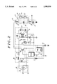
- FIG. 2 comprises a schematic depiction of an electronic ballast as configured in accordance with the invention.
- the electronic ballast described herein couples to a pair of series connected gas discharge lamps 11. (Although a pair is shown, one or more lamps may be connected in their stead.)
- the electronic ballast couples to a source of alternating current 12 through a user operable switch 13, as is well understood in the art.
- a rectifier 14 receives the alternating current and provides a full wave rectified output. This output couples to both a power factor corrector and inverter 16 and to a PWM driver 18 via a resistor 21 and a boot strap capacitor 22 (the boot strap capacitor 22 serves, amongst other things, to filter the rectified alternating current signal provided by the rectifier 14).
- the PWM driver 18 is coupled to and controls operability of the power factor corrector and inverter 16.
- a voltage clamp 19 couples to the power factor corrector and inverter 16 and also couples, via a conductive path 20, to the boot strap capacitor 22.
- the power factor corrector and inverter 16 also couples to an output 17 which in turn couples to the gas discharge lamps 11.
- the boot strap capacitor 22 has a corresponding charging rate (which charging rate is dependent upon a variety of factors, including the capacitance of the boot strap capacitor 22 itself).
- the high voltage storage capacitor 23 has a corresponding charging rate in the context of the circuit depicted.
- the charging rate for the boot strap capacitor 22 is slower than the charging rate for the high voltage storage capacitor 23.
- the high voltage storage capacitor have a charging rate that does not exceed 10 milliseconds
- the boot strap capacitor 22 should have a charging rate that does not exceed 500 milliseconds.
- longer timing rates may give rise to delay start times that are, in turn, interpreted by a user as indicative of failure.
- the boot strap capacitor 22 must have a relatively low capacitance value in order to ensure that the charging rate for the boot strap capacitor 22 will not exceed 500 milliseconds. Therefore, although the boot strap capacitor 22 will charge relatively quickly, it will not contain a large quantity of stored energy.
- an energizing signal is provided to the PWM driver 18, which in turn initially activates the power factor corrector and inverter 16.
- the power factor corrector and inverter 16 becomes active, a drive signal is provided to the gas discharge lamps 11.
- the voltage clamp 19 responds to operation of the power factor controller and inverter 16 by establishing a conductive path 20 that selectively couples the high voltage storage capacitor 23 to the boot strap capacitor 22, thereby delivering energy from the high voltage storage capacitor 23 to the boot strap capacitor 22 and hence sustaining continued operation of the PWM driver 18.
- the boot strap capacitor 22 will charge relatively quickly (from the standpoint of an observer) and can provide sufficient energy to the PWM driver 18 to cause initial activation of the electronic ballast. .Its smaller size, ensures rapid initial activation. However, the boot strap capacitor 22 cannot long sustain operation of the PWM driver 18. Since, upon activation, a path 20 is formed between the two capacitors 22 and 23 through the voltage clamp 19, and since the high voltage storage capacitor 23 completed its full charge before the boot strap capacitor 22, energy from the high voltage storage capacitor 23 is thereafter made available to the boot strap capacitor 22 to sustain continued operation of the PWM driver 18 and hence continued energization of the gas discharge lamp 11.
- the rectifier 14 can be comprised of a diode bridge 38.
- the power factor corrector and inverter 16 includes a circuit comprised of a 6 mH (microhenry) inductor 39 and a 0.1 mF capacitor 41.
- the circuit couples to a diode 40 and a MJE18004 bipolar transistor 42. (As an aside, the power factor corrector and inverter 16 contains this transistor 42 as the only active lo component in its design).
- the PWM driver 18 includes a drive element 43 and a pulse width modulation control element 44, provided through use of an MC3845 integrated circuit, as is well understood in the art.
- the boot strap capacitor 22 in this embodiment comprises a 47 mF capacitor. Resistor 21 that couples the boot strap capacitor 22 to the rectifier comprises a 220,000 ohm resistor.
- the voltage clamp comprises a transformer having a primary winding 46 and two secondary windings 47 and 52.
- a 0.1 mF capacitor 48 couples across the primary 46 and the first secondary 47.
- a ferrite bead 49 (for electromagnetic interference suppression) and a diode 51 are disposed as configured.
- the second secondary 52 couples to a diode 53 and to the path 20 to the boot strap capacitor 22 as described above.
- the high voltage storage capacitor 23 couples to the primary 46 and comprises a 22 mF capacitor.
- energy from the high storage capacitor 23 is inductively coupled through the primary 46 and second secondary 52 via the path 20 to the boot strap capacitor 22 when the voltage clamp circuit 19 is rendered fully operational via the transistor 42 of the power factor corrector and inverter 16.
- the output 17 includes two inductors 33, 36 and two capacitors 34, 37 configured to form appropriate resonant circuits suited to properly maintained energization of the gas discharge lamp 11.
- the lamps 31 and 32 are themselves coupled into the electronic ballast circuitry via appropriate gas discharge lamp terminals 30, as well understood in the art.
Abstract
Description
Claims (7)
Priority Applications (3)
| Application Number | Priority Date | Filing Date | Title |
|---|---|---|---|
| US08/270,333 US5586016A (en) | 1994-07-05 | 1994-07-05 | Circuit for quickly energizing electronic ballast |
| DE69523827T DE69523827T2 (en) | 1994-07-05 | 1995-06-19 | Circuit for operating an electronic switching device without delay |
| EP95109442A EP0691799B1 (en) | 1994-07-05 | 1995-06-19 | Circuit for quickly energizing electronic ballast |
Applications Claiming Priority (1)
| Application Number | Priority Date | Filing Date | Title |
|---|---|---|---|
| US08/270,333 US5586016A (en) | 1994-07-05 | 1994-07-05 | Circuit for quickly energizing electronic ballast |
Publications (1)
| Publication Number | Publication Date |
|---|---|
| US5586016A true US5586016A (en) | 1996-12-17 |
Family
ID=23030898
Family Applications (1)
| Application Number | Title | Priority Date | Filing Date |
|---|---|---|---|
| US08/270,333 Expired - Lifetime US5586016A (en) | 1994-07-05 | 1994-07-05 | Circuit for quickly energizing electronic ballast |
Country Status (3)
| Country | Link |
|---|---|
| US (1) | US5586016A (en) |
| EP (1) | EP0691799B1 (en) |
| DE (1) | DE69523827T2 (en) |
Cited By (4)
| Publication number | Priority date | Publication date | Assignee | Title |
|---|---|---|---|---|
| US5822201A (en) * | 1995-03-06 | 1998-10-13 | Kijima Co., Ltd. | Double-ended inverter with boost transformer having output side impedance element |
| US6301129B1 (en) * | 1999-09-22 | 2001-10-09 | Sony Corporation | Switching power supply circuit |
| US20030230990A1 (en) * | 2002-04-19 | 2003-12-18 | Phi Hong Electronics (Shanghai) Co. Ltd. | Electronic ballast using cut & save technology |
| US8456867B1 (en) * | 2011-12-01 | 2013-06-04 | Telefonaktiebolaget Lm Ericsson (Publ) | Start-up procedure for an isolated switched mode power supply |
Families Citing this family (3)
| Publication number | Priority date | Publication date | Assignee | Title |
|---|---|---|---|---|
| US5834902A (en) * | 1996-04-18 | 1998-11-10 | U.S. Philips Corporation | Discharge lamp igniting and operating curcuit having interference signal suppression from 9 KHz to 100 MHz |
| US5910708A (en) * | 1996-09-06 | 1999-06-08 | General Electric Company | Gas discharge lamp ballast circuit with complementary converter switches |
| NO318911B1 (en) | 2003-11-14 | 2005-05-23 | Tandberg Telecom As | Distributed composition of real-time media |
Citations (1)
| Publication number | Priority date | Publication date | Assignee | Title |
|---|---|---|---|---|
| US5363020A (en) * | 1993-02-05 | 1994-11-08 | Systems And Service International, Inc. | Electronic power controller |
Family Cites Families (5)
| Publication number | Priority date | Publication date | Assignee | Title |
|---|---|---|---|---|
| US4623960A (en) * | 1984-10-15 | 1986-11-18 | At&T Bell Laboratories | Bias power source energized by tertiary winding including hysteresis characteristic for disabling the power switch when a minimum base drive signal can no longer be maintained |
| JPS62166777A (en) * | 1986-01-16 | 1987-07-23 | Sanken Electric Co Ltd | Dc-dc converter |
| KR910002377B1 (en) * | 1987-09-18 | 1991-04-20 | 가부시기가이샤 하다찌세이사구쇼 | Switching power supply |
| KR920005724Y1 (en) * | 1990-05-11 | 1992-08-20 | 삼성전자 주식회사 | Circuit for switching mode power supply |
| US5285369A (en) * | 1992-09-01 | 1994-02-08 | Power Integrations, Inc. | Switched mode power supply integrated circuit with start-up self-biasing |
-
1994
- 1994-07-05 US US08/270,333 patent/US5586016A/en not_active Expired - Lifetime
-
1995
- 1995-06-19 DE DE69523827T patent/DE69523827T2/en not_active Expired - Fee Related
- 1995-06-19 EP EP95109442A patent/EP0691799B1/en not_active Expired - Lifetime
Patent Citations (1)
| Publication number | Priority date | Publication date | Assignee | Title |
|---|---|---|---|---|
| US5363020A (en) * | 1993-02-05 | 1994-11-08 | Systems And Service International, Inc. | Electronic power controller |
Cited By (5)
| Publication number | Priority date | Publication date | Assignee | Title |
|---|---|---|---|---|
| US5822201A (en) * | 1995-03-06 | 1998-10-13 | Kijima Co., Ltd. | Double-ended inverter with boost transformer having output side impedance element |
| US6301129B1 (en) * | 1999-09-22 | 2001-10-09 | Sony Corporation | Switching power supply circuit |
| US20030230990A1 (en) * | 2002-04-19 | 2003-12-18 | Phi Hong Electronics (Shanghai) Co. Ltd. | Electronic ballast using cut & save technology |
| US6933684B2 (en) | 2002-04-19 | 2005-08-23 | Phi Hong Electronics (Shanghai) Co. Ltd. | Electronic ballast using cut and save technology |
| US8456867B1 (en) * | 2011-12-01 | 2013-06-04 | Telefonaktiebolaget Lm Ericsson (Publ) | Start-up procedure for an isolated switched mode power supply |
Also Published As
| Publication number | Publication date |
|---|---|
| EP0691799A2 (en) | 1996-01-10 |
| DE69523827D1 (en) | 2001-12-20 |
| EP0691799B1 (en) | 2001-11-14 |
| EP0691799A3 (en) | 1997-12-03 |
| DE69523827T2 (en) | 2002-04-11 |
Similar Documents
| Publication | Publication Date | Title |
|---|---|---|
| US4005335A (en) | High frequency power source for fluorescent lamps and the like | |
| US4999547A (en) | Ballast for high pressure sodium lamps having constant line and lamp wattage | |
| US5235254A (en) | Fluorescent lamp supply circuit | |
| US5767631A (en) | Power supply and electronic ballast with low-cost inverter bootstrap power source | |
| EP0765108B1 (en) | High intensity discharge lamp lighting device | |
| US4525650A (en) | Starting and operating method and apparatus for discharge lamps | |
| US6700331B2 (en) | Control circuit for dimming fluorescent lamps | |
| KR0137181B1 (en) | Discharge lamp lighting device | |
| US4187448A (en) | Discharge lamp lighting device | |
| US5528111A (en) | Ballast circuit for powering gas discharge lamp | |
| US4484107A (en) | Discharge lamp lighting device and system | |
| US5586016A (en) | Circuit for quickly energizing electronic ballast | |
| JP3042470B2 (en) | Lighting device for discharge lamp and lighting device for discharge lamp | |
| US5945784A (en) | High intensity discharge ballast | |
| JPH04342993A (en) | Discharge lamp lighting device | |
| JPH0945490A (en) | Lighting device for discharge lamp | |
| KR20050062671A (en) | A high voltage ballast for resonant inverter | |
| KR100351436B1 (en) | Electronic Ballast for High Voltage Discharge Lamp | |
| JP2003203790A (en) | Discharge lamp lighting device | |
| JP2744008B2 (en) | Power converter | |
| KR840000104Y1 (en) | Electronic starting circuit of neon tube | |
| JP3378117B2 (en) | Lighting device | |
| JPH05284735A (en) | Power supply unit and discharge lamp lighting device | |
| JPH09308255A (en) | Discharge lamp lighting apparatus | |
| JP3003154B2 (en) | Discharge lamp lighting device |
Legal Events
| Date | Code | Title | Description |
|---|---|---|---|
| AS | Assignment |
Owner name: MOTOROLA LIGHTING, INC., ILLINOIS Free format text: ASSIGNMENT OF ASSIGNORS INTEREST;ASSIGNORS:KONOPKA, JOHN G.;PRIEGNITZ, ROBERT A.;REEL/FRAME:007572/0893 Effective date: 19940630 |
|
| STCF | Information on status: patent grant |
Free format text: PATENTED CASE |
|
| FEPP | Fee payment procedure |
Free format text: PAYOR NUMBER ASSIGNED (ORIGINAL EVENT CODE: ASPN); ENTITY STATUS OF PATENT OWNER: LARGE ENTITY |
|
| AS | Assignment |
Owner name: OSRAM SYLVANIA INC., MASSACHUSETTS Free format text: ASSIGNMENT OF ASSIGNORS INTEREST;ASSIGNOR:MOTOROLA, INC.;REEL/FRAME:010648/0827 Effective date: 20000229 |
|
| FPAY | Fee payment |
Year of fee payment: 4 |
|
| FEPP | Fee payment procedure |
Free format text: PAYOR NUMBER ASSIGNED (ORIGINAL EVENT CODE: ASPN); ENTITY STATUS OF PATENT OWNER: LARGE ENTITY Free format text: PAYER NUMBER DE-ASSIGNED (ORIGINAL EVENT CODE: RMPN); ENTITY STATUS OF PATENT OWNER: LARGE ENTITY |
|
| FPAY | Fee payment |
Year of fee payment: 8 |
|
| FPAY | Fee payment |
Year of fee payment: 12 |
|
| AS | Assignment |
Owner name: OSRAM SYLVANIA INC., MASSACHUSETTS Free format text: MERGER;ASSIGNOR:OSRAM SYLVANIA INC.;REEL/FRAME:025546/0415 Effective date: 20100902 |