US5622596A - High density selective SiO2 :Si3 N4 etching using a stoichiometrically altered nitride etch stop - Google Patents
High density selective SiO2 :Si3 N4 etching using a stoichiometrically altered nitride etch stop Download PDFInfo
- Publication number
- US5622596A US5622596A US08/435,063 US43506395A US5622596A US 5622596 A US5622596 A US 5622596A US 43506395 A US43506395 A US 43506395A US 5622596 A US5622596 A US 5622596A
- Authority
- US
- United States
- Prior art keywords
- nitride
- etch stop
- layer
- etching
- etch
- Prior art date
- Legal status (The legal status is an assumption and is not a legal conclusion. Google has not performed a legal analysis and makes no representation as to the accuracy of the status listed.)
- Expired - Fee Related
Links
Images


Classifications
-
- H—ELECTRICITY
- H01—ELECTRIC ELEMENTS
- H01L—SEMICONDUCTOR DEVICES NOT COVERED BY CLASS H10
- H01L21/00—Processes or apparatus adapted for the manufacture or treatment of semiconductor or solid state devices or of parts thereof
- H01L21/02—Manufacture or treatment of semiconductor devices or of parts thereof
- H01L21/04—Manufacture or treatment of semiconductor devices or of parts thereof the devices having at least one potential-jump barrier or surface barrier, e.g. PN junction, depletion layer or carrier concentration layer
- H01L21/18—Manufacture or treatment of semiconductor devices or of parts thereof the devices having at least one potential-jump barrier or surface barrier, e.g. PN junction, depletion layer or carrier concentration layer the devices having semiconductor bodies comprising elements of Group IV of the Periodic System or AIIIBV compounds with or without impurities, e.g. doping materials
- H01L21/30—Treatment of semiconductor bodies using processes or apparatus not provided for in groups H01L21/20 - H01L21/26
- H01L21/302—Treatment of semiconductor bodies using processes or apparatus not provided for in groups H01L21/20 - H01L21/26 to change their surface-physical characteristics or shape, e.g. etching, polishing, cutting
- H01L21/304—Mechanical treatment, e.g. grinding, polishing, cutting
-
- H—ELECTRICITY
- H01—ELECTRIC ELEMENTS
- H01L—SEMICONDUCTOR DEVICES NOT COVERED BY CLASS H10
- H01L21/00—Processes or apparatus adapted for the manufacture or treatment of semiconductor or solid state devices or of parts thereof
- H01L21/02—Manufacture or treatment of semiconductor devices or of parts thereof
- H01L21/04—Manufacture or treatment of semiconductor devices or of parts thereof the devices having at least one potential-jump barrier or surface barrier, e.g. PN junction, depletion layer or carrier concentration layer
- H01L21/18—Manufacture or treatment of semiconductor devices or of parts thereof the devices having at least one potential-jump barrier or surface barrier, e.g. PN junction, depletion layer or carrier concentration layer the devices having semiconductor bodies comprising elements of Group IV of the Periodic System or AIIIBV compounds with or without impurities, e.g. doping materials
- H01L21/30—Treatment of semiconductor bodies using processes or apparatus not provided for in groups H01L21/20 - H01L21/26
- H01L21/31—Treatment of semiconductor bodies using processes or apparatus not provided for in groups H01L21/20 - H01L21/26 to form insulating layers thereon, e.g. for masking or by using photolithographic techniques; After treatment of these layers; Selection of materials for these layers
- H01L21/3105—After-treatment
- H01L21/311—Etching the insulating layers by chemical or physical means
- H01L21/31105—Etching inorganic layers
-
- Y—GENERAL TAGGING OF NEW TECHNOLOGICAL DEVELOPMENTS; GENERAL TAGGING OF CROSS-SECTIONAL TECHNOLOGIES SPANNING OVER SEVERAL SECTIONS OF THE IPC; TECHNICAL SUBJECTS COVERED BY FORMER USPC CROSS-REFERENCE ART COLLECTIONS [XRACs] AND DIGESTS
- Y10—TECHNICAL SUBJECTS COVERED BY FORMER USPC
- Y10S—TECHNICAL SUBJECTS COVERED BY FORMER USPC CROSS-REFERENCE ART COLLECTIONS [XRACs] AND DIGESTS
- Y10S438/00—Semiconductor device manufacturing: process
- Y10S438/97—Specified etch stop material
Definitions
- the present invention generally relates to semiconductor chip manufacture and, more particularly, to selective etching of SiO 2 to Si 3 N 4 using a stoichiometrically altered nitride etch stop.
- Ultra Large Scale Integrated (ULSI) circuit applications require reactive ion etch (RIE) processes which will etch oxide highly selective to nitride. While this has been demonstrated on planar surfaces, stringent ground rules in advanced applications require high nitride selectivity over exposed corners. The most common example of this is where a diffusion contact overlaps a gate. Selectivities greater than 12 to 1 at the exposed corner of the gate are required to prevent leakage from the gate to the contact.
- RIE reactive ion etch
- Thick nitride spacers on the edges of the device have been introduced to absorb any nitride erosion which may take place during the etch. This procedure, however, cannot be used in applications with very high packing densities.
- an integrated circuit is prepared with a conformal layer of nitride as an etch stop.
- a nitride etch stop layer is deposited over a corner of the etch susceptible material.
- This nitride etch stop layer is characterized by a nitride formed stoichiometrically with the addition of a material that imparts improved etch selectivity over oxide.
- An oxide layer is deposited over the nitride layers, an aperture is patterned above the oxide, and then etching is performed though the oxide, stopping on the nitride layer without erosion.
- the nitride in the conformal layer is altered by increasing the concentration of silicon or by adding Al 2 O 3 or Y 2 O 3 .
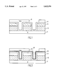
- FIG. 1 is a cross section of a borderless contact structure after high selectivity oxide:nitride etch process and resist strip;
- FIG. 2 is a cross section of a borderless contact structure as in FIG. 1 with the addition of the proposed altered film;
- FIG. 3 is a graph of the capacitance-voltage curves for thin samples of silicon rich nitride having varying atomic percentages of silicon.
- FIG. 4 is a graph of the current-voltage curves for thin samples of silicon rich nitride having varying atomic percentages of silicon.
- FIG. 1 there is shown a typical feature requiring high oxide to nitride selectivity, consisting of a silicon substrate 1 with gate electrodes 2, being about 2000-8000 ⁇ in thickness.
- the gate electrodes 2 have a nitride cap 3, and electrodes and substrate are lined with a thin conformal nitride layer 4, which is usually between 100-1000 ⁇ in thickness.
- These features are then filled with a dielectric 5, such as silicon dioxide, planarized, and patterned with photo resist and etched.
- a stoichiometrically altered nitride layer as either all or part of the conformal nitride layer is introduced.
- a feature having a silicon substrate 1 gate electrodes 2, cap 3 and conformal nitride 4 layers is constructed.
- An altered conformal nitride layer 6 is added.
- This structure can be constructed having the altered conformal nitride layer 6 replacing the first conformal nitride layer 4.
- This same type of altered nitride could additionally be included in the cap 3 of the gate electrode 2.
- This nitride layer consists of higher concentrations of some materials, such as silicon and hydrogen, which add substantial selectivity to the nitride film during the etch process, without substantially changing the dielectric properties of the material.
- High selectivity oxide etch processes are commonly known throughout the semiconductor industry. Specifically, selectivities to silicon greater than 40:1 have been obtained on planar surfaces. These types of selectivities can be readily achieved in advanced etch systems, such as the AME Centura Oxide Etcher, because of their independent RF biasing, low pressure, and low fluorine content polymers when scavenging media are employed. High selectivity to polysilicon, for example, can even be obtained over topography for extended overetch times. This is noteworthy because when topography is introduced, ions impinging on exposed corners act to remove the deposited polymer, allowing sputtering of the polysilicon corner.
- the Si 3 N 4 composition is altered such that it contains a higher percentage of silicon, in the range of 43.1 to 65 atomic percent.
- the material is insulating throughout this range as revealed by capacitance-voltage characteristics as is shown in the graph of FIG. 3.
- the bottom most curve 21 represents a sample having 43.1 atomic percent silicon and the top most curve 22 represents a sample having 67 atomic percent silicon.
- the stoichiometry can be monitored using the optical properties, in particular, the refractive index of the film.
- the refractive index for samples having 43 to 60% atomic percent of silicon ranged from 1.90 to 2.11. Samples having 65 to 67 atomic percent silicon had a refractive index of 2.20.
- a shift in capacitance-voltage is shown by arrow 23. This shift is due to charge trapping. However, charge trapping, which can have a detrimental effect on device stability, becomes more severe at the higher silicon levels as seen from the shift in capacitance-voltage characteristics, shown in the graph of FIG. 4. An increase in the shift of the capacitance-voltage characteristics corresponds to an increased amount of trapped charge.
- This curve represents samples having 43.1 to 67 atomic percent of silicon for a thin, between 300-400 ⁇ , nitride, as well.
- the best concentration range for maximizing etch selectivity while minimizing conductivity is 50 to 60 atomic percent.
- this nitride retains the insulator characteristics which will prevent shorts, it will also have the increased selectivity required for a manufacturable process.
- Adjustment of the nitride stoichiometry is easily accomplished by adjusting the SiH 4 flow with respect to NH 3 or N 2 ratios during a Plasma Enhanced Chemical Vapor Deposition (PECVD) process. Concentrations ranging from about 50-60 atomic percent can be obtained in this manner with minimal process optimization. Stoichiometrically altered nitride films can also be deposited by sputtering or by other chemical vapor deposition processes or can be formed by ion implantation.
- PECVD Plasma Enhanced Chemical Vapor Deposition
- This technique while demonstrated with silicon-rich nitride, can be expanded to include other types of selectivity enhancers. These may include hydrogen, which may act as a polymer source during the etch.
- Other known etch stop materials such as Al 2 O 3 , or Y 2 O 3 , also can be incorporated into a nitride film by sputtering, CVD, or ion implantation, which will allow it to behave as a nitride, but have enough characteristics of the additive film to improve selectivity in an oxide etch chemistry.
- This process adds minimal complexity.
- This stoichiometrically altered film can be added on top of the existing LPCVD nitride, or, if reliability is acceptable, can be used as the sole etch stop, requiring no additional process steps.
- this invention is desirable because it means implementation of a borderless contact process is dependent on a controlled feature, not the etch process alone. While high density plasma etching may be critical to etch high aspect ratios and obtain selectivity to nitride on plana surfaces, it is not in itself a means to obtain a borderless contact.
Abstract
Description
Claims (5)
Priority Applications (5)
| Application Number | Priority Date | Filing Date | Title |
|---|---|---|---|
| US08/435,063 US5622596A (en) | 1995-05-08 | 1995-05-08 | High density selective SiO2 :Si3 N4 etching using a stoichiometrically altered nitride etch stop |
| TW085100436A TW301777B (en) | 1995-05-08 | 1996-01-16 | |
| EP96480038A EP0742584A3 (en) | 1995-05-08 | 1996-04-04 | High density selective SiO2:Si3N4 etching using a stoichiometrically altered nitride etch stop layer |
| KR1019960012358A KR100209041B1 (en) | 1995-05-08 | 1996-04-23 | High density selective sio2: si3n4 etching using a stoichiometrically altered nitride etch stop |
| JP10911196A JP3193632B2 (en) | 1995-05-08 | 1996-04-30 | Oxide etching method |
Applications Claiming Priority (1)
| Application Number | Priority Date | Filing Date | Title |
|---|---|---|---|
| US08/435,063 US5622596A (en) | 1995-05-08 | 1995-05-08 | High density selective SiO2 :Si3 N4 etching using a stoichiometrically altered nitride etch stop |
Publications (1)
| Publication Number | Publication Date |
|---|---|
| US5622596A true US5622596A (en) | 1997-04-22 |
Family
ID=23726810
Family Applications (1)
| Application Number | Title | Priority Date | Filing Date |
|---|---|---|---|
| US08/435,063 Expired - Fee Related US5622596A (en) | 1995-05-08 | 1995-05-08 | High density selective SiO2 :Si3 N4 etching using a stoichiometrically altered nitride etch stop |
Country Status (5)
| Country | Link |
|---|---|
| US (1) | US5622596A (en) |
| EP (1) | EP0742584A3 (en) |
| JP (1) | JP3193632B2 (en) |
| KR (1) | KR100209041B1 (en) |
| TW (1) | TW301777B (en) |
Cited By (15)
| Publication number | Priority date | Publication date | Assignee | Title |
|---|---|---|---|---|
| US5880006A (en) * | 1998-05-22 | 1999-03-09 | Vlsi Technology, Inc. | Method for fabrication of a semiconductor device |
| US5880005A (en) * | 1997-10-23 | 1999-03-09 | Taiwan Semiconductor Manufacturing Company, Ltd. | Method for forming a tapered profile insulator shape |
| US5897372A (en) * | 1995-11-01 | 1999-04-27 | Micron Technology, Inc. | Formation of a self-aligned integrated circuit structure using silicon-rich nitride as a protective layer |
| US5994215A (en) * | 1996-10-24 | 1999-11-30 | International Business Machines Corporation | Method for suppression pattern distortion associated with BPSG reflow |
| US6001268A (en) * | 1997-06-05 | 1999-12-14 | International Business Machines Corporation | Reactive ion etching of alumina/TiC substrates |
| US6004875A (en) * | 1995-11-15 | 1999-12-21 | Micron Technology, Inc. | Etch stop for use in etching of silicon oxide |
| US6040619A (en) * | 1995-06-07 | 2000-03-21 | Advanced Micro Devices | Semiconductor device including antireflective etch stop layer |
| US6063711A (en) * | 1998-04-28 | 2000-05-16 | Taiwan Semiconductor Manufacturing Company | High selectivity etching stop layer for damascene process |
| US6136700A (en) * | 1996-12-20 | 2000-10-24 | Texas Instruments Incorporated | Method for enhancing the performance of a contact |
| US6207575B1 (en) * | 1998-02-20 | 2001-03-27 | Advanced Micro Devices, Inc. | Local interconnect etch characterization using AFM |
| US6268299B1 (en) | 2000-09-25 | 2001-07-31 | International Business Machines Corporation | Variable stoichiometry silicon nitride barrier films for tunable etch selectivity and enhanced hyrogen permeability |
| US6316349B1 (en) * | 1998-11-12 | 2001-11-13 | Hyundai Electronics Industries Co., Ltd. | Method for forming contacts of semiconductor devices |
| US6602434B1 (en) * | 1998-03-27 | 2003-08-05 | Applied Materials, Inc. | Process for etching oxide using hexafluorobutadiene or related fluorocarbons and manifesting a wide process window |
| US20040175934A1 (en) * | 2003-03-04 | 2004-09-09 | International Business Machines Corporation | Method for improving etch selectivity effects in dual damascene processing |
| EP1630249A2 (en) | 2004-08-30 | 2006-03-01 | Air Products And Chemicals, Inc. | Process for chemical vapor deposition of silicon nitride. |
Families Citing this family (1)
| Publication number | Priority date | Publication date | Assignee | Title |
|---|---|---|---|---|
| US9293379B2 (en) | 2009-09-03 | 2016-03-22 | Raytheon Company | Semiconductor structure with layers having different hydrogen contents |
Citations (8)
| Publication number | Priority date | Publication date | Assignee | Title |
|---|---|---|---|---|
| US4367119A (en) * | 1980-08-18 | 1983-01-04 | International Business Machines Corporation | Planar multi-level metal process with built-in etch stop |
| US4447824A (en) * | 1980-08-18 | 1984-05-08 | International Business Machines Corporation | Planar multi-level metal process with built-in etch stop |
| US4543707A (en) * | 1983-06-30 | 1985-10-01 | Kabushiki Kaisha | Method of forming through holes by differential etching of stacked silicon oxynitride layers |
| JPS62205645A (en) * | 1986-03-06 | 1987-09-10 | Fujitsu Ltd | Manufacture of semiconductor device |
| EP0265584A2 (en) * | 1986-10-30 | 1988-05-04 | International Business Machines Corporation | Method and materials for etching silicon dioxide using silicon nitride or silicon rich dioxide as an etch barrier |
| US5443998A (en) * | 1989-08-01 | 1995-08-22 | Cypress Semiconductor Corp. | Method of forming a chlorinated silicon nitride barrier layer |
| US5468987A (en) * | 1991-03-06 | 1995-11-21 | Semiconductor Energy Laboratory Co., Ltd. | Semiconductor device and method for forming the same |
| US5470793A (en) * | 1991-06-28 | 1995-11-28 | Sgs-Thomson Microelectronics, Inc. | Method of via formation for the multilevel interconnect integrated circuits |
Family Cites Families (5)
| Publication number | Priority date | Publication date | Assignee | Title |
|---|---|---|---|---|
| US4299862A (en) * | 1979-11-28 | 1981-11-10 | General Motors Corporation | Etching windows in thick dielectric coatings overlying semiconductor device surfaces |
| US4656729A (en) * | 1985-03-25 | 1987-04-14 | International Business Machines Corp. | Dual electron injection structure and process with self-limiting oxidation barrier |
| US5252515A (en) * | 1991-08-12 | 1993-10-12 | Taiwan Semiconductor Manufacturing Company | Method for field inversion free multiple layer metallurgy VLSI processing |
| US5252516A (en) * | 1992-02-20 | 1993-10-12 | International Business Machines Corporation | Method for producing interlevel stud vias |
| US5324690A (en) * | 1993-02-01 | 1994-06-28 | Motorola Inc. | Semiconductor device having a ternary boron nitride film and a method for forming the same |
-
1995
- 1995-05-08 US US08/435,063 patent/US5622596A/en not_active Expired - Fee Related
-
1996
- 1996-01-16 TW TW085100436A patent/TW301777B/zh active
- 1996-04-04 EP EP96480038A patent/EP0742584A3/en not_active Withdrawn
- 1996-04-23 KR KR1019960012358A patent/KR100209041B1/en not_active IP Right Cessation
- 1996-04-30 JP JP10911196A patent/JP3193632B2/en not_active Expired - Fee Related
Patent Citations (8)
| Publication number | Priority date | Publication date | Assignee | Title |
|---|---|---|---|---|
| US4367119A (en) * | 1980-08-18 | 1983-01-04 | International Business Machines Corporation | Planar multi-level metal process with built-in etch stop |
| US4447824A (en) * | 1980-08-18 | 1984-05-08 | International Business Machines Corporation | Planar multi-level metal process with built-in etch stop |
| US4543707A (en) * | 1983-06-30 | 1985-10-01 | Kabushiki Kaisha | Method of forming through holes by differential etching of stacked silicon oxynitride layers |
| JPS62205645A (en) * | 1986-03-06 | 1987-09-10 | Fujitsu Ltd | Manufacture of semiconductor device |
| EP0265584A2 (en) * | 1986-10-30 | 1988-05-04 | International Business Machines Corporation | Method and materials for etching silicon dioxide using silicon nitride or silicon rich dioxide as an etch barrier |
| US5443998A (en) * | 1989-08-01 | 1995-08-22 | Cypress Semiconductor Corp. | Method of forming a chlorinated silicon nitride barrier layer |
| US5468987A (en) * | 1991-03-06 | 1995-11-21 | Semiconductor Energy Laboratory Co., Ltd. | Semiconductor device and method for forming the same |
| US5470793A (en) * | 1991-06-28 | 1995-11-28 | Sgs-Thomson Microelectronics, Inc. | Method of via formation for the multilevel interconnect integrated circuits |
Cited By (23)
| Publication number | Priority date | Publication date | Assignee | Title |
|---|---|---|---|---|
| US6040619A (en) * | 1995-06-07 | 2000-03-21 | Advanced Micro Devices | Semiconductor device including antireflective etch stop layer |
| US5897372A (en) * | 1995-11-01 | 1999-04-27 | Micron Technology, Inc. | Formation of a self-aligned integrated circuit structure using silicon-rich nitride as a protective layer |
| US6117767A (en) * | 1995-11-01 | 2000-09-12 | Micron Technology, Inc. | Method of forming an integrated circuit structure |
| US6222257B1 (en) | 1995-11-15 | 2001-04-24 | Micron Technology, Inc. | Etch stop for use in etching of silicon oxide |
| US6555896B2 (en) | 1995-11-15 | 2003-04-29 | Micron Technology, Inc. | Etch stop for use in etching of silicon oxide |
| US6004875A (en) * | 1995-11-15 | 1999-12-21 | Micron Technology, Inc. | Etch stop for use in etching of silicon oxide |
| US6013943A (en) * | 1995-11-15 | 2000-01-11 | Micron Technology, Inc. | Etch stop for use in etching of silicon oxide |
| US6232218B1 (en) | 1995-11-15 | 2001-05-15 | Micron Technology, Inc. | Etch stop for use in etching of silicon oxide |
| US5994215A (en) * | 1996-10-24 | 1999-11-30 | International Business Machines Corporation | Method for suppression pattern distortion associated with BPSG reflow |
| US6495439B1 (en) * | 1996-10-24 | 2002-12-17 | International Business Machines Corporation | Method for suppressing pattern distortion associated with BPSG reflow and integrated circuit chip formed thereby |
| US6136700A (en) * | 1996-12-20 | 2000-10-24 | Texas Instruments Incorporated | Method for enhancing the performance of a contact |
| US6001268A (en) * | 1997-06-05 | 1999-12-14 | International Business Machines Corporation | Reactive ion etching of alumina/TiC substrates |
| US5880005A (en) * | 1997-10-23 | 1999-03-09 | Taiwan Semiconductor Manufacturing Company, Ltd. | Method for forming a tapered profile insulator shape |
| US6207575B1 (en) * | 1998-02-20 | 2001-03-27 | Advanced Micro Devices, Inc. | Local interconnect etch characterization using AFM |
| US6602434B1 (en) * | 1998-03-27 | 2003-08-05 | Applied Materials, Inc. | Process for etching oxide using hexafluorobutadiene or related fluorocarbons and manifesting a wide process window |
| US6063711A (en) * | 1998-04-28 | 2000-05-16 | Taiwan Semiconductor Manufacturing Company | High selectivity etching stop layer for damascene process |
| US5880006A (en) * | 1998-05-22 | 1999-03-09 | Vlsi Technology, Inc. | Method for fabrication of a semiconductor device |
| US6309948B1 (en) * | 1998-05-22 | 2001-10-30 | Vlsi Technology, Inc. | Method for fabrication of a semiconductor device |
| US6316349B1 (en) * | 1998-11-12 | 2001-11-13 | Hyundai Electronics Industries Co., Ltd. | Method for forming contacts of semiconductor devices |
| US6268299B1 (en) | 2000-09-25 | 2001-07-31 | International Business Machines Corporation | Variable stoichiometry silicon nitride barrier films for tunable etch selectivity and enhanced hyrogen permeability |
| US20040175934A1 (en) * | 2003-03-04 | 2004-09-09 | International Business Machines Corporation | Method for improving etch selectivity effects in dual damascene processing |
| EP1630249A2 (en) | 2004-08-30 | 2006-03-01 | Air Products And Chemicals, Inc. | Process for chemical vapor deposition of silicon nitride. |
| US20060045986A1 (en) * | 2004-08-30 | 2006-03-02 | Hochberg Arthur K | Silicon nitride from aminosilane using PECVD |
Also Published As
| Publication number | Publication date |
|---|---|
| KR100209041B1 (en) | 1999-07-15 |
| EP0742584A3 (en) | 1997-10-08 |
| EP0742584A2 (en) | 1996-11-13 |
| JP3193632B2 (en) | 2001-07-30 |
| TW301777B (en) | 1997-04-01 |
| KR960042996A (en) | 1996-12-21 |
| JPH08306658A (en) | 1996-11-22 |
Similar Documents
| Publication | Publication Date | Title |
|---|---|---|
| US5622596A (en) | High density selective SiO2 :Si3 N4 etching using a stoichiometrically altered nitride etch stop | |
| US6162737A (en) | Films doped with carbon for use in integrated circuit technology | |
| US5292673A (en) | Method of manufacturing a semiconductor device | |
| US6541280B2 (en) | High K dielectric film | |
| US4559693A (en) | Process for fabricating field effect transistors | |
| EP0050973B1 (en) | Masking process for semiconductor devices using a polymer film | |
| US20080079083A1 (en) | Semiconductor device and a method of manufacture therefor | |
| US6417083B1 (en) | Methods for manufacturing semiconductor devices | |
| KR100275733B1 (en) | Method for forming MOS transistor having bi-layer spacer | |
| US6537906B1 (en) | Methods for fabricating semiconductor devices | |
| US6441464B1 (en) | Gate oxide stabilization by means of germanium components in gate conductor | |
| US6191016B1 (en) | Method of patterning a layer for a gate electrode of a MOS transistor | |
| US20050136688A1 (en) | Method of inhibiting degradation of gate oxide film | |
| JP2001102455A (en) | Method for forming a contact-point opening in dielectrics layer of semiconductor device | |
| KR20040006459A (en) | Method for improvement etching of hard mask | |
| KR100272182B1 (en) | Gate polysilicon etching method for forming dual gate electrode of semiconductor device | |
| KR100866119B1 (en) | Method for forming dual gate electrode | |
| KR100634267B1 (en) | Method for forming of device isolation region in a semiconductor device | |
| KR100275110B1 (en) | Method for forming tungsten polycide | |
| KR100300528B1 (en) | Capacitor and its manufacturing method | |
| KR100398574B1 (en) | Method for forming gate spacer of semiconductor device | |
| US7365020B2 (en) | Method for etching upper metal of capacitator | |
| KR20030051036A (en) | Transistor in a semiconductor device and method of manufacturing thereof | |
| KR20050063049A (en) | Method for fabricating semiconductor device | |
| KR20000039795A (en) | Method of forming gate electrode of semiconductor device |
Legal Events
| Date | Code | Title | Description |
|---|---|---|---|
| AS | Assignment |
Owner name: INTERNATIONAL BUSINESS MACHINES CORPORATION, NEW Y Free format text: ASSIGNMENT OF ASSIGNORS INTEREST;ASSIGNORS:ARMACOST, MICHAEL D.;DOBUZINSKY, DAVID;GAMBINO, JEFFREY;AND OTHERS;REEL/FRAME:007487/0845;SIGNING DATES FROM 19950504 TO 19950508 |
|
| FEPP | Fee payment procedure |
Free format text: PAYOR NUMBER ASSIGNED (ORIGINAL EVENT CODE: ASPN); ENTITY STATUS OF PATENT OWNER: LARGE ENTITY |
|
| FPAY | Fee payment |
Year of fee payment: 4 |
|
| FEPP | Fee payment procedure |
Free format text: PAYER NUMBER DE-ASSIGNED (ORIGINAL EVENT CODE: RMPN); ENTITY STATUS OF PATENT OWNER: LARGE ENTITY Free format text: PAYOR NUMBER ASSIGNED (ORIGINAL EVENT CODE: ASPN); ENTITY STATUS OF PATENT OWNER: LARGE ENTITY |
|
| FPAY | Fee payment |
Year of fee payment: 8 |
|
| REMI | Maintenance fee reminder mailed | ||
| LAPS | Lapse for failure to pay maintenance fees | ||
| STCH | Information on status: patent discontinuation |
Free format text: PATENT EXPIRED DUE TO NONPAYMENT OF MAINTENANCE FEES UNDER 37 CFR 1.362 |
|
| FP | Lapsed due to failure to pay maintenance fee |
Effective date: 20090422 |