US5632437A - Method of centering a lid seal clip - Google Patents
Method of centering a lid seal clip Download PDFInfo
- Publication number
- US5632437A US5632437A US08/538,907 US53890795A US5632437A US 5632437 A US5632437 A US 5632437A US 53890795 A US53890795 A US 53890795A US 5632437 A US5632437 A US 5632437A
- Authority
- US
- United States
- Prior art keywords
- lid
- package
- pressure foot
- pin
- boat
- Prior art date
- Legal status (The legal status is an assumption and is not a legal conclusion. Google has not performed a legal analysis and makes no representation as to the accuracy of the status listed.)
- Expired - Lifetime
Links
Images


Classifications
-
- H—ELECTRICITY
- H01—ELECTRIC ELEMENTS
- H01L—SEMICONDUCTOR DEVICES NOT COVERED BY CLASS H10
- H01L24/00—Arrangements for connecting or disconnecting semiconductor or solid-state bodies; Methods or apparatus related thereto
- H01L24/80—Methods for connecting semiconductor or other solid state bodies using means for bonding being attached to, or being formed on, the surface to be connected
- H01L24/83—Methods for connecting semiconductor or other solid state bodies using means for bonding being attached to, or being formed on, the surface to be connected using a layer connector
-
- H—ELECTRICITY
- H01—ELECTRIC ELEMENTS
- H01L—SEMICONDUCTOR DEVICES NOT COVERED BY CLASS H10
- H01L24/00—Arrangements for connecting or disconnecting semiconductor or solid-state bodies; Methods or apparatus related thereto
- H01L24/01—Means for bonding being attached to, or being formed on, the surface to be connected, e.g. chip-to-package, die-attach, "first-level" interconnects; Manufacturing methods related thereto
- H01L24/26—Layer connectors, e.g. plate connectors, solder or adhesive layers; Manufacturing methods related thereto
- H01L24/28—Structure, shape, material or disposition of the layer connectors prior to the connecting process
- H01L24/29—Structure, shape, material or disposition of the layer connectors prior to the connecting process of an individual layer connector
-
- H—ELECTRICITY
- H01—ELECTRIC ELEMENTS
- H01L—SEMICONDUCTOR DEVICES NOT COVERED BY CLASS H10
- H01L2224/00—Indexing scheme for arrangements for connecting or disconnecting semiconductor or solid-state bodies and methods related thereto as covered by H01L24/00
- H01L2224/01—Means for bonding being attached to, or being formed on, the surface to be connected, e.g. chip-to-package, die-attach, "first-level" interconnects; Manufacturing methods related thereto
- H01L2224/26—Layer connectors, e.g. plate connectors, solder or adhesive layers; Manufacturing methods related thereto
- H01L2224/28—Structure, shape, material or disposition of the layer connectors prior to the connecting process
- H01L2224/29—Structure, shape, material or disposition of the layer connectors prior to the connecting process of an individual layer connector
- H01L2224/29001—Core members of the layer connector
- H01L2224/29099—Material
- H01L2224/2919—Material with a principal constituent of the material being a polymer, e.g. polyester, phenolic based polymer, epoxy
-
- H—ELECTRICITY
- H01—ELECTRIC ELEMENTS
- H01L—SEMICONDUCTOR DEVICES NOT COVERED BY CLASS H10
- H01L2224/00—Indexing scheme for arrangements for connecting or disconnecting semiconductor or solid-state bodies and methods related thereto as covered by H01L24/00
- H01L2224/80—Methods for connecting semiconductor or other solid state bodies using means for bonding being attached to, or being formed on, the surface to be connected
- H01L2224/83—Methods for connecting semiconductor or other solid state bodies using means for bonding being attached to, or being formed on, the surface to be connected using a layer connector
- H01L2224/8319—Arrangement of the layer connectors prior to mounting
-
- H—ELECTRICITY
- H01—ELECTRIC ELEMENTS
- H01L—SEMICONDUCTOR DEVICES NOT COVERED BY CLASS H10
- H01L2224/00—Indexing scheme for arrangements for connecting or disconnecting semiconductor or solid-state bodies and methods related thereto as covered by H01L24/00
- H01L2224/80—Methods for connecting semiconductor or other solid state bodies using means for bonding being attached to, or being formed on, the surface to be connected
- H01L2224/83—Methods for connecting semiconductor or other solid state bodies using means for bonding being attached to, or being formed on, the surface to be connected using a layer connector
- H01L2224/838—Bonding techniques
- H01L2224/8385—Bonding techniques using a polymer adhesive, e.g. an adhesive based on silicone, epoxy, polyimide, polyester
-
- H—ELECTRICITY
- H01—ELECTRIC ELEMENTS
- H01L—SEMICONDUCTOR DEVICES NOT COVERED BY CLASS H10
- H01L2924/00—Indexing scheme for arrangements or methods for connecting or disconnecting semiconductor or solid-state bodies as covered by H01L24/00
- H01L2924/01—Chemical elements
- H01L2924/01006—Carbon [C]
-
- H—ELECTRICITY
- H01—ELECTRIC ELEMENTS
- H01L—SEMICONDUCTOR DEVICES NOT COVERED BY CLASS H10
- H01L2924/00—Indexing scheme for arrangements or methods for connecting or disconnecting semiconductor or solid-state bodies as covered by H01L24/00
- H01L2924/01—Chemical elements
- H01L2924/01033—Arsenic [As]
-
- H—ELECTRICITY
- H01—ELECTRIC ELEMENTS
- H01L—SEMICONDUCTOR DEVICES NOT COVERED BY CLASS H10
- H01L2924/00—Indexing scheme for arrangements or methods for connecting or disconnecting semiconductor or solid-state bodies as covered by H01L24/00
- H01L2924/01—Chemical elements
- H01L2924/01082—Lead [Pb]
-
- H—ELECTRICITY
- H01—ELECTRIC ELEMENTS
- H01L—SEMICONDUCTOR DEVICES NOT COVERED BY CLASS H10
- H01L2924/00—Indexing scheme for arrangements or methods for connecting or disconnecting semiconductor or solid-state bodies as covered by H01L24/00
- H01L2924/013—Alloys
- H01L2924/014—Solder alloys
-
- H—ELECTRICITY
- H01—ELECTRIC ELEMENTS
- H01L—SEMICONDUCTOR DEVICES NOT COVERED BY CLASS H10
- H01L2924/00—Indexing scheme for arrangements or methods for connecting or disconnecting semiconductor or solid-state bodies as covered by H01L24/00
- H01L2924/06—Polymers
- H01L2924/0665—Epoxy resin
-
- H—ELECTRICITY
- H01—ELECTRIC ELEMENTS
- H01L—SEMICONDUCTOR DEVICES NOT COVERED BY CLASS H10
- H01L2924/00—Indexing scheme for arrangements or methods for connecting or disconnecting semiconductor or solid-state bodies as covered by H01L24/00
- H01L2924/06—Polymers
- H01L2924/078—Adhesive characteristics other than chemical
- H01L2924/07802—Adhesive characteristics other than chemical not being an ohmic electrical conductor
-
- H—ELECTRICITY
- H01—ELECTRIC ELEMENTS
- H01L—SEMICONDUCTOR DEVICES NOT COVERED BY CLASS H10
- H01L2924/00—Indexing scheme for arrangements or methods for connecting or disconnecting semiconductor or solid-state bodies as covered by H01L24/00
- H01L2924/10—Details of semiconductor or other solid state devices to be connected
- H01L2924/11—Device type
- H01L2924/14—Integrated circuits
Definitions
- the present invention relates to integrated circuit (i.c.) fabrication methods and apparatus.
- the invention relates to methods and supporting apparatus to apply centered, perpendicular force to an integrated circuit package lid during the hermetic seal curing process interval.
- Integrated circuits are frequently packaged for product assembly in sealed casements having only connector leads or points exposed for external conduit connection. Such packages are fabricated in laminated tiers with a dielectric base plate and a ceramic or plastic lid plate. Between the lamination tiers are two or more additional layers that route and electrically isolate electrical paths between specific circuit junctures on the integrated circuit chip and a corresponding connector lead or pin. The actual circuit chip is potted within a cavity surrounded by the laminations.
- the lid may be hermetically sealed by an epoxy adhesive or metallic solder, for example.
- the adhesive or solder is applied to either or both faces of the lid and substrate and cured or set while the lid is held down under a predetermined force applied by a spring clip.
- excessive seal failures occur because of insufficient or inadequate distribution of seal force.
- an object of the invention to provide a method for sealing an i.c. package lid that centers the sealing force normal to the lid plane.
- Another object of the present invention is to provide a method using a sealing load clip that may be reliably positioned at a predetermined location on an assembly boat and i.c. package lid.
- the invention method includes the steps of retracting the pressure foot of a secondary loading jig against the resilient bias of a spring and positioning the jig across the assembly boat to mesh a plurality of index pins on the loading jig with corresponding index sockets on the assembly boat. In meshing position, the pressure foot is confined to spring force application along the central axis of the lid.
- a package fabrication boat utilized by the method includes a plurality of package alignment sockets, each of which laterally confine and restrain movement of a respective package during the course of integrated circuit processing.
- Process control index holes in the top surface and side rails of the boat are aligned coordinately with the package sockets. Pins secured to the force application clip mesh with appropriate pairs of index holes to secure an aligned position of the force clip.
- a force applying pressure foot forms one end of a spring loaded rocker bar.
- the bar oscillates about a rocker axis that is parallel to the package lid surface but is biased in the pressure foot rotational direction for loading against the package lid.
- Another embodiment of the invention includes a pressure foot secured to one end of an alignment shaft.
- the force clip includes structural guides to confine the alignment shaft and limit movement to axial reciprocation.
- a compression spring biases the pressure foot toward the package lid when the force clip is attached to an assembly boat.
- FIG. 1 is an end elevation relating to the invention first embodiment in operative combination with a package assembly boat.
- FIG. 2 is a partially sectioned detail relating to the first embodiment combination.
- FIG. 3 is an exploded assembly view of an integrated circuit package.
- FIG. 4 is a plan view relating to an integrated circuit package assembly boat.
- FIG. 5 is an end elevation relating to the package assembly boat.
- FIG. 6 is a side elevation relating to the package assembly boat.
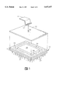
- FIG. 7 is a pictorial view relating to a first embodiment of the invention.
- FIG. 8 is a side elevation relating to the invention first embodiment.
- FIG. 9 is a plan view relating to the invention first embodiment.
- FIG. 10 is a pictorial view relating to a second embodiment of the invention.
- FIG. 11 is a side elevation relating to the invention second embodiment.
- FIG. 12 is a top plan view relating to the invention second embodiment.
- FIG. 13 is a side elevation relating to the invention second embodiment engaged with a package assembly boat.
- FIG. 1 a loading clip 10 is shown as operationally engaged with an integrated circuit (i.c.) package 12 and a corresponding i.c. package assembly jig 14 characterized in the art as a "boat",
- an i.c. package 12 includes a package base 20 formed by a laminated plurality of layers that are capped by a lid 22.
- the i.c. chip 18 is potted within the stepped void 24 formed within the center of the laminated base 20.
- the laminated layers 20 provide conductor separation between the i.c. chip and connector pins 26 projecting from the package bottom.
- FIGS. 4, 5, and 6 illustrate the characteristics of an assembly boat 14 to include a multiplicity of package sockets 30 which are apertures in the boat top plate 34.
- Four tabs 32 around the perimeter of each socket 30 are integral extensions of the top plate 34.
- the spacial distances between oppositely facing edges 27 are dimensioned to receive the pin 26 base of a package 12 therebetween for lateral confinement and vertical support.
- Also in the boat top plate 34 along the longitudinal sides of the top plate are respective rows of index sockets 36.
- Additional index sockets 38 are formed in the boat side rails 35. It will be noted that a pair of index sockets 36 and 38 are aligned with the transverse centerlines 31 respective to each socket 30. Between each centerline 31, four, equidistant, index socket intervals are provided for this example.
- a second jig in the cooperative assembly is a loading jig or spring force clip 10 comprising a base plate 40 having a pair of axle pedestals 42 projecting therefrom to support an axle 44. Also projecting from the base plate 40 are a pair of index pins 46 and 47. Pin 46 is turned substantially parallel with the base plate 40 whereas pin 47 projects substantially normal to the base plate 40 plane.
- Pin 46 is flanked by abutment shoulders 48 and pin 47 is flanked by abutment shoulders 49. As shown by the assembly elevation of FIG. 1, the dimensional locations of pins 46 and 47 and their corresponding abutment shoulders are coordinated to the index sockets 36 and 38 of the assembly boat 14.
- Clamping bar 50 includes a pressure foot 52 at one end and a hand pad 53 at the other end on opposite sides of the axle 44. Legs 54 rotatively support the bar 50 over the axle 44.
- a helically coiled tensile spring wrapped about axle 44 includes reaction arms 56 to resiliently bias rotation of the clamping bar about the axle 44. Such rotational bias is opposed at the pressure foot 52 by the i.c. package 12.
- the spring clip components are dimensionally coordinated to position the point of pressure foot 52 engagement against the i.c. package lid 22 in the plane of the axle 44 axis and along the axis 58 at the center of the chip void 24.
- the i.c. package lid is resiliently clamped with a perpendicular bearing load of known value, preferably in the range of about 1.5 to 5 pounds at substantially the optimum position to provide a uniformly distributed curing pressure between the lid 22 and the lower lamination 20.
- the i.c. package assembly (FIG. 3) is completed by application of an adhesive or solder 28 to the interfacing surfaces respective to the package lid 22 and the uppermost surface of the lamination 20.
- This assembly is positioned in a package socket 30 with the connector pins 26 laterally caged between the internal edges 27 of tabs 32. In most cases, this socket position will locate the i.c. assembly 12 center point in the transverse plane 31 which bisects the socket 30 and corresponding edge rail sockets 38 and top plate sockets 36.
- the loading jig 10 is combined with the boat by depressing the clamping bar 50 at the hand pad 53 to lift the pressure foot 52 away from the base plate 40.
- the pin 46 is meshed with the edge rail socket 38 along an angular line of penetration until the shoulder 48 abuts the face of rail 35.
- the loading jig 10 With the shoulder 48 against the rail 35, the loading jig 10 is rotated about the shoulder/rail engagement line thereby bringing the index pin 47 into meshing penetration of the corresponding top plate socket 36 until the shoulder 49 seats against the bottom face of the top plate 34.
- the base edge 37 of rail 35 engages the transversely flat surface of base plate 40 to further immobilize and locate the loading jig 10 relative to the boat 14.
- the clamping bar is gently released to engage the lid covered i.c. package 12 with a constant and calibrated compression force applied at or very near the lid 22 center along the load axis 58.
- Such assembly may be repeated for an i.c. package in each of the boat sockets 30 in a particular boat 14.
- a completely assembled boat jig 14 secured by the present invention is stable against abrupt movement encountered by a boat jig in a further process conveyance line.
- FIGS. 10-13 A second spring clip embodiment of the invention 16 is illustrated by FIGS. 10-13 to include a semi-box frame 60 having two pairs of legs 62 and 64, respectively, to laterally stabilize the frame 60 against the top plate 34 of the boat 14.
- indexing arms 66 and 68 At respective ends of the frame 60 are indexing arms 66 and 68.
- Index arm 68 has a structurally rigid relationship to the semi-box frame 60 and stabilizing legs 62 whereas the indexing arm 68 is rotatable about the axis of axle pin 69.
- rotation of index arm 68 is spring biased to maintain an engagement force against a boat rail 35.
- Indexing arm 66 carries index socket pin 70 which meshes with an appropriate edge rail index socket 38.
- the pivoting indexing arm 68 carries indexing pin 78 for engaging sockets 38 in the opposite side rail.
- the bottom edges of the stabilizing legs 62 and 64 are coordinated with the index pins 70 and 72 to secure a boat 14 to the semibox frame 60 structure with the boat top plate 34 perpendicular to the reciprocation axis 74 of a pressure foot 76. Also, the separation distance between the indexing arms and their relative spacing from the axis 74 is aligned for coincidence of the axis 74 with the lid load axis 58.
- Pressure foot 76 is secured to the distal end of a guide rod 80 and urged away from the semi box frame by a coiled compression spring 78 wound about the rod 80.
- a cross-pin or yoke bar 82 is secured to the guide rod 80 and rides on the ramp 84 edges 86.
- a detent pocket 88 is formed in the upper edge surfaces to stabilize the yoke bar 82 and guide rod 80 at the upper position at which the spring 78 is compressed and the pressure foot 76 is withdrawn from the i.c. package 12 surface.
- This relationship of the yoke bar 82 saddled into the pocket 88 is attained by sliding the ramp frame 87 to an extreme position in the direction of the arrowhead 89 (FIG. 10). When pushed to the extreme position in the opposite direction of arrowhead 90 (FIG. 13), the yoke bar 82 rides down on the ramp edges 86 and permits the compression spring 78 to load the pressure foot 76 against the i.c. package lid.
- the i.c. package and lid are positioned on the boat 14 socket 30 with adhesive or solder 28 applied between the lid 22 and lower lamination 20.
- the pivotable index arm 68 is rotated about the axis 69 against a spring bias by manually squeezing between the thumb pad 71 and an upstanding tab of ramp frame 87, the pressure foot 76 and attached guide rod 80 are lifted against the bias of spring 78 and cocked in the detent 88.
- the loading jig 16 is aligned to insert the index socket pin 70 into the desired rail socket 38 located along the transverse center plane 31. This alignment will place the base of legs 62 and 64 on the surface of boat top plate 34.
- the pivotable index arm 68 is then released to mesh the index pin 72 with the axially opposite rail socket 38 thereby setting the loading jig 16 with the boat 14 and package 12.
- the ramp frame 87 is shifted to the left as viewed at FIG. 13 and the pressure foot 76 is released to engage the i.c. package 12.
Abstract
Description
Claims (13)
Priority Applications (1)
| Application Number | Priority Date | Filing Date | Title |
|---|---|---|---|
| US08/538,907 US5632437A (en) | 1995-10-04 | 1995-10-04 | Method of centering a lid seal clip |
Applications Claiming Priority (1)
| Application Number | Priority Date | Filing Date | Title |
|---|---|---|---|
| US08/538,907 US5632437A (en) | 1995-10-04 | 1995-10-04 | Method of centering a lid seal clip |
Publications (1)
| Publication Number | Publication Date |
|---|---|
| US5632437A true US5632437A (en) | 1997-05-27 |
Family
ID=24148923
Family Applications (1)
| Application Number | Title | Priority Date | Filing Date |
|---|---|---|---|
| US08/538,907 Expired - Lifetime US5632437A (en) | 1995-10-04 | 1995-10-04 | Method of centering a lid seal clip |
Country Status (1)
| Country | Link |
|---|---|
| US (1) | US5632437A (en) |
Cited By (5)
| Publication number | Priority date | Publication date | Assignee | Title |
|---|---|---|---|---|
| US6003757A (en) * | 1998-04-30 | 1999-12-21 | International Business Machines Corporation | Apparatus for transferring solder bumps and method of using |
| US6206270B1 (en) * | 1999-12-30 | 2001-03-27 | Te Shih Huang | Method of assembling needles for eyebrow makeup |
| US6222151B1 (en) | 1998-11-09 | 2001-04-24 | Lockheed Martin Corporation | Low profile welding fixture |
| CN101885123A (en) * | 2010-07-19 | 2010-11-17 | 杭州凯尔达电焊机有限公司 | Modularized centralized positioning welding tool |
| CN103157941A (en) * | 2011-12-14 | 2013-06-19 | 苏州工业园区高登威科技有限公司 | Integrated circuit (IC) line welding machine |
Citations (4)
| Publication number | Priority date | Publication date | Assignee | Title |
|---|---|---|---|---|
| US2444312A (en) * | 1945-05-01 | 1948-06-29 | Rca Corp | Art of sealing metal casings enclosing vibratile elements |
| US4595794A (en) * | 1984-03-19 | 1986-06-17 | At&T Bell Laboratories | Component mounting apparatus |
| SU1391839A1 (en) * | 1986-11-27 | 1988-04-30 | Предприятие П/Я А-1891 | Diffusion welding unit |
| US4871106A (en) * | 1988-10-28 | 1989-10-03 | Wharff Charles R | Non-dedicated pallet assembly for wave soldering packaged integrated circuits |
-
1995
- 1995-10-04 US US08/538,907 patent/US5632437A/en not_active Expired - Lifetime
Patent Citations (4)
| Publication number | Priority date | Publication date | Assignee | Title |
|---|---|---|---|---|
| US2444312A (en) * | 1945-05-01 | 1948-06-29 | Rca Corp | Art of sealing metal casings enclosing vibratile elements |
| US4595794A (en) * | 1984-03-19 | 1986-06-17 | At&T Bell Laboratories | Component mounting apparatus |
| SU1391839A1 (en) * | 1986-11-27 | 1988-04-30 | Предприятие П/Я А-1891 | Diffusion welding unit |
| US4871106A (en) * | 1988-10-28 | 1989-10-03 | Wharff Charles R | Non-dedicated pallet assembly for wave soldering packaged integrated circuits |
Non-Patent Citations (2)
| Title |
|---|
| Salvadore V. Caruso, et al., "Investigation of Discrete Component Chip Mounting Technology for Hybrid Microelectronic Circuits," N75-25044, National Technical Information Service, Springfield, VA, May 1975. |
| Salvadore V. Caruso, et al., Investigation of Discrete Component Chip Mounting Technology for Hybrid Microelectronic Circuits, N75 25044, National Technical Information Service, Springfield, VA, May 1975. * |
Cited By (6)
| Publication number | Priority date | Publication date | Assignee | Title |
|---|---|---|---|---|
| US6003757A (en) * | 1998-04-30 | 1999-12-21 | International Business Machines Corporation | Apparatus for transferring solder bumps and method of using |
| US6222151B1 (en) | 1998-11-09 | 2001-04-24 | Lockheed Martin Corporation | Low profile welding fixture |
| US6206270B1 (en) * | 1999-12-30 | 2001-03-27 | Te Shih Huang | Method of assembling needles for eyebrow makeup |
| CN101885123A (en) * | 2010-07-19 | 2010-11-17 | 杭州凯尔达电焊机有限公司 | Modularized centralized positioning welding tool |
| CN101885123B (en) * | 2010-07-19 | 2012-04-18 | 杭州凯尔达电焊机有限公司 | Modularized centralized positioning welding tool |
| CN103157941A (en) * | 2011-12-14 | 2013-06-19 | 苏州工业园区高登威科技有限公司 | Integrated circuit (IC) line welding machine |
Similar Documents
| Publication | Publication Date | Title |
|---|---|---|
| US5665652A (en) | Method for manufacturing a semiconductor device wherein electrodes on a semiconductor chip are electrically connected to lead terminals by plating bonding | |
| US5055971A (en) | Magnetic component using core clip arrangement operative for facilitating pick and place surface mount | |
| US9240339B2 (en) | Substrate holder, substrate holder unit, substrate transport apparatus, and substrate bonding apparatus | |
| US5180974A (en) | Semiconductor testing and shipping system | |
| EP1063727A2 (en) | IC socket | |
| US5598775A (en) | Centering lid seal clip apparatus | |
| US5632437A (en) | Method of centering a lid seal clip | |
| JP2855719B2 (en) | Semiconductor device | |
| US5695593A (en) | Method of centering a high pressure lid seal | |
| JPH0418436B2 (en) | ||
| US5716493A (en) | High pressure lid seal clip apparatus | |
| US3092893A (en) | Fabrication of semiconductor devices | |
| US3859715A (en) | System and method for attaching semiconductor dice to leads | |
| JP2575643B2 (en) | Electronic device surface mounting device | |
| US4600611A (en) | Film carrier for manufacturing semiconductor devices | |
| US5291127A (en) | Chip-lifetime testing instrument for semiconductor devices | |
| US4709847A (en) | Device for assembling electrical components on a terminal carrier plate | |
| US11112452B2 (en) | IC tray and test jig | |
| KR20000002375A (en) | Tape aligner for fbga package | |
| CN219725945U (en) | Tube shell clamping jig and wire bonding device | |
| KR100264319B1 (en) | Device for alignment between picker and test socket | |
| JPS6242526Y2 (en) | ||
| JPS5984561A (en) | Socket for flat ic | |
| JPH06180345A (en) | Tray for housing semiconductor device and device and method for testing semiconductor device | |
| JPH0124634Y2 (en) |
Legal Events
| Date | Code | Title | Description |
|---|---|---|---|
| AS | Assignment |
Owner name: LSI LOGI CORPORATION, CALIFORNIA Free format text: ASSIGNMENT OF ASSIGNORS INTEREST;ASSIGNORS:VONGFUANGFOO, SUTEE;BORUTA, MIREK;KIRKPATRICK, GALEN;REEL/FRAME:007695/0387 Effective date: 19950929 |
|
| STCF | Information on status: patent grant |
Free format text: PATENTED CASE |
|
| CC | Certificate of correction | ||
| FPAY | Fee payment |
Year of fee payment: 4 |
|
| FPAY | Fee payment |
Year of fee payment: 8 |
|
| FEPP | Fee payment procedure |
Free format text: PAYOR NUMBER ASSIGNED (ORIGINAL EVENT CODE: ASPN); ENTITY STATUS OF PATENT OWNER: LARGE ENTITY Free format text: PAYER NUMBER DE-ASSIGNED (ORIGINAL EVENT CODE: RMPN); ENTITY STATUS OF PATENT OWNER: LARGE ENTITY |
|
| FPAY | Fee payment |
Year of fee payment: 12 |
|
| AS | Assignment |
Owner name: DEUTSCHE BANK AG NEW YORK BRANCH, AS COLLATERAL AG Free format text: PATENT SECURITY AGREEMENT;ASSIGNORS:LSI CORPORATION;AGERE SYSTEMS LLC;REEL/FRAME:032856/0031 Effective date: 20140506 |
|
| AS | Assignment |
Owner name: AVAGO TECHNOLOGIES GENERAL IP (SINGAPORE) PTE. LTD Free format text: ASSIGNMENT OF ASSIGNORS INTEREST;ASSIGNOR:LSI CORPORATION;REEL/FRAME:035390/0388 Effective date: 20140814 |
|
| AS | Assignment |
Owner name: LSI CORPORATION, CALIFORNIA Free format text: TERMINATION AND RELEASE OF SECURITY INTEREST IN PATENT RIGHTS (RELEASES RF 032856-0031);ASSIGNOR:DEUTSCHE BANK AG NEW YORK BRANCH, AS COLLATERAL AGENT;REEL/FRAME:037684/0039 Effective date: 20160201 Owner name: AGERE SYSTEMS LLC, PENNSYLVANIA Free format text: TERMINATION AND RELEASE OF SECURITY INTEREST IN PATENT RIGHTS (RELEASES RF 032856-0031);ASSIGNOR:DEUTSCHE BANK AG NEW YORK BRANCH, AS COLLATERAL AGENT;REEL/FRAME:037684/0039 Effective date: 20160201 |
|
| AS | Assignment |
Owner name: BELL SEMICONDUCTOR, LLC, ILLINOIS Free format text: ASSIGNMENT OF ASSIGNORS INTEREST;ASSIGNORS:AVAGO TECHNOLOGIES GENERAL IP (SINGAPORE) PTE. LTD.;BROADCOM CORPORATION;REEL/FRAME:044886/0766 Effective date: 20171208 |
|
| AS | Assignment |
Owner name: CORTLAND CAPITAL MARKET SERVICES LLC, AS COLLATERA Free format text: SECURITY INTEREST;ASSIGNORS:HILCO PATENT ACQUISITION 56, LLC;BELL SEMICONDUCTOR, LLC;BELL NORTHERN RESEARCH, LLC;REEL/FRAME:045216/0020 Effective date: 20180124 |
|
| AS | Assignment |
Owner name: BELL NORTHERN RESEARCH, LLC, ILLINOIS Free format text: RELEASE BY SECURED PARTY;ASSIGNOR:CORTLAND CAPITAL MARKET SERVICES LLC;REEL/FRAME:059723/0382 Effective date: 20220401 Owner name: BELL SEMICONDUCTOR, LLC, ILLINOIS Free format text: RELEASE BY SECURED PARTY;ASSIGNOR:CORTLAND CAPITAL MARKET SERVICES LLC;REEL/FRAME:059723/0382 Effective date: 20220401 Owner name: HILCO PATENT ACQUISITION 56, LLC, ILLINOIS Free format text: RELEASE BY SECURED PARTY;ASSIGNOR:CORTLAND CAPITAL MARKET SERVICES LLC;REEL/FRAME:059723/0382 Effective date: 20220401 |