US5686752A - Semiconductor device having a CMOS element as a buffer - Google Patents
Semiconductor device having a CMOS element as a buffer Download PDFInfo
- Publication number
- US5686752A US5686752A US08/576,614 US57661495A US5686752A US 5686752 A US5686752 A US 5686752A US 57661495 A US57661495 A US 57661495A US 5686752 A US5686752 A US 5686752A
- Authority
- US
- United States
- Prior art keywords
- mos transistor
- semiconductor device
- voltage level
- pmos
- potential
- Prior art date
- Legal status (The legal status is an assumption and is not a legal conclusion. Google has not performed a legal analysis and makes no representation as to the accuracy of the status listed.)
- Expired - Lifetime
Links
Images


Classifications
-
- H—ELECTRICITY
- H03—ELECTRONIC CIRCUITRY
- H03K—PULSE TECHNIQUE
- H03K19/00—Logic circuits, i.e. having at least two inputs acting on one output; Inverting circuits
- H03K19/003—Modifications for increasing the reliability for protection
- H03K19/00315—Modifications for increasing the reliability for protection in field-effect transistor circuits
-
- H—ELECTRICITY
- H01—ELECTRIC ELEMENTS
- H01L—SEMICONDUCTOR DEVICES NOT COVERED BY CLASS H10
- H01L27/00—Devices consisting of a plurality of semiconductor or other solid-state components formed in or on a common substrate
- H01L27/02—Devices consisting of a plurality of semiconductor or other solid-state components formed in or on a common substrate including semiconductor components specially adapted for rectifying, oscillating, amplifying or switching and having at least one potential-jump barrier or surface barrier; including integrated passive circuit elements with at least one potential-jump barrier or surface barrier
- H01L27/04—Devices consisting of a plurality of semiconductor or other solid-state components formed in or on a common substrate including semiconductor components specially adapted for rectifying, oscillating, amplifying or switching and having at least one potential-jump barrier or surface barrier; including integrated passive circuit elements with at least one potential-jump barrier or surface barrier the substrate being a semiconductor body
- H01L27/08—Devices consisting of a plurality of semiconductor or other solid-state components formed in or on a common substrate including semiconductor components specially adapted for rectifying, oscillating, amplifying or switching and having at least one potential-jump barrier or surface barrier; including integrated passive circuit elements with at least one potential-jump barrier or surface barrier the substrate being a semiconductor body including only semiconductor components of a single kind
- H01L27/085—Devices consisting of a plurality of semiconductor or other solid-state components formed in or on a common substrate including semiconductor components specially adapted for rectifying, oscillating, amplifying or switching and having at least one potential-jump barrier or surface barrier; including integrated passive circuit elements with at least one potential-jump barrier or surface barrier the substrate being a semiconductor body including only semiconductor components of a single kind including field-effect components only
- H01L27/088—Devices consisting of a plurality of semiconductor or other solid-state components formed in or on a common substrate including semiconductor components specially adapted for rectifying, oscillating, amplifying or switching and having at least one potential-jump barrier or surface barrier; including integrated passive circuit elements with at least one potential-jump barrier or surface barrier the substrate being a semiconductor body including only semiconductor components of a single kind including field-effect components only the components being field-effect transistors with insulated gate
- H01L27/092—Devices consisting of a plurality of semiconductor or other solid-state components formed in or on a common substrate including semiconductor components specially adapted for rectifying, oscillating, amplifying or switching and having at least one potential-jump barrier or surface barrier; including integrated passive circuit elements with at least one potential-jump barrier or surface barrier the substrate being a semiconductor body including only semiconductor components of a single kind including field-effect components only the components being field-effect transistors with insulated gate complementary MIS field-effect transistors
- H01L27/0921—Means for preventing a bipolar, e.g. thyristor, action between the different transistor regions, e.g. Latchup prevention
Definitions
- the present invention relates to a semiconductor device and, more particularly, a semiconductor device incorporating an output buffer therein constituted of a CMOS (Complementary Metal Oxide Semiconductor) IC.
- CMOS Complementary Metal Oxide Semiconductor
- CMOS output buffer A semiconductor device which has an output buffer constituted of a conventional CMOS (hereafter referred to as "CMOS output buffer”) is formed on, for example, a P type substrate.
- CMOS output buffer is provided with a P channel type field effect transistor (hereafter referred to as "PMOS”) and an N channel type field effect transistor (hereafter referred to as "NMOS”) which are connected in series between a power supply potential Vcc and a ground potential Vss.
- PMOS P channel type field effect transistor
- NMOS N channel type field effect transistor
- An N type well is formed on the P type substrate.
- the PMOS is formed in the N type well and the N type well is biased to the power supply potential Vcc.
- the P type substrate is biased to a negative potential Vbb so that a circuit between the N type well and the P type substrate is not forward-biased even if a potential of an input pin undershoots.
- the semiconductor device having the conventional CMOS output buffer includes a shortcoming as described below.
- the output buffer constituted of the CMOS includes a shortcoming that a latch-up resistance against a positive surge caused due to static electricity or the like is low.
- FIG. 1 is a cross sectional view of the output buffer for depicting a latch-up phenomenon and the following describes a problem of the prior art, referring to this drawing.
- FIG. 1 shows a P type substrate 1 and an N type well 2 formed therein.
- a PMOS having a drain 3, a source 4 and a gate 5 is formed in the N type well 2 and an NMOS having a drain 6, a source 7 and a gate 8 is formed on the P type substrate 1.
- An active region 9 connected to the bias potential Vcc is formed in an N type well 2 and an active region 10 connected to the bias potential Vbb is formed on the P type substrate 1.
- the CMOS output buffer having such configuration includes parasitic bipolar transistors 11, 12, 13, 14 and 15 as shown in FIG. 1.
- Transistors 11 and 12 respectively serve as an n-p-n type bipolar transistor and transistors 13 to 15 respectively serve as a p-n-p type bipolar transistor.
- the ON voltage of the bipolar transistor that is, a built-in potential is BP (generally, approximately 0.8 V) and a threshold voltage of the PMOS is Vtp.
- BP generally, approximately 0.8 V
- Vtp a threshold voltage of the PMOS
- transistors 13 and 14 turn on before the PMOS turns on.
- a current flowing through the transistor 14 flows into the power supply Vcc and a current flowing through the transistor 13 flows into the substrate 1.
- the currents flowing in the transistors 13 and 14 have different potentials and therefore the current flowing in the transistor 13 is larger than that in the transistor 14. In other words, a greater part of the current flows into the substrate 1.
- the current supplying capacity of a bias potential Vbb generating circuit (not shown) is not so high because a stand-by current is controlled to be low.
- a current flowing into the substrate 1 due to a positive surge is compared with the current supplying capacity of the bias potential Vbb generating circuit, the current flowing into the substrate 1 is absolutely larger and, since the resistance value of the substrate resistance 16 is generally so large, the potential of the base of the transistor 11 steeply rises.
- the potential Vbb of the substrate 1 steeply rises and the transistor 11 turns on.
- the current flows in a path of the power supply Vcc ⁇ N type well resistor 17 ⁇ transistor 11 ⁇ ground potential Vss and this current serves as a trigger current of the latch-up phenomenon.
- the N type well resistor 17 has a comparatively large resistance and, when the trigger current flows, a potential difference in accordance with a quantity of trigger current is caused at both end points A and B of the resistor 17. Therefore, the base potential of the transistor 15 becomes low.
- the potential of the emitter of the transistor 15 is the power supply potential Vcc and, if a difference potential which is produced between the base and the emitter is larger than the voltage BP, the transistor 15 turns on. Accordingly, a current flows from the power supply potential Vcc to the substrate 1, and the potential Vbb of the substrate 1 rises again.
- An object of the present invention is to solve the shortcomings of the prior art as described above and to provide a semiconductor device which excels in reliability and durability by improving a latch-up tolerance thereof.
- a semiconductor device comprises a first MOS transistor of a first conductivity type and a second MOS transistor of a second conductivity type, the first MOS transistor and the second MOS transistor being connected in series between a first power supply potential and a second power supply potential lower than the first power supply potential, wherein a back gate bias of the first MOS transistor is set to a third power supply potential higher than the first power supply potential.
- a semiconductor device comprises a first MOS transistor of a first conductivity type and a second MOS transistor of a second conductivity type, the first MOS transistor and the second MOS transistor being connected in series between a first power supply potential and a second power supply potential lower than said first power supply potential, and an active region for setting a back gate bias of the first MOS transistor formed so as to surround the first MOS transistor in a well in which the first MOS transistor is formed.
- a semiconductor device comprises a first MOS transistor of a first conductivity type, a second MOS transistor of a second conductivity type, the first MOS transistor and the second MOS transistor being connected in series between a first power supply potential and a second power supply potential lower than the first power supply potential, and a third MOS transistor of the first conductivity type connected in parallel with the first MOS transistor and provided between the first power supply potential and the second power supply potential, the gate of the third MOS transistor being connected to the first power supply potential and a back gate bias of the third MOS transistor being set at a third power supply potential higher than the first power supply potential.
- the semiconductor device is configured as described above and, therefore, in a first aspect of the present invention, the base potential of a parasitic bipolar transistor disposed between the first MOS transistor in the output buffer and the substrate is higher than in a case that the back gate bias of the first MOS transistor is set to the first power supply potential even when a trigger current is produced by a surge voltage. Accordingly, the current which flows through this parasitic transistor is reduced.
- a well resistance is reduced and a potential difference caused due to the well resistance becomes small by forming an active region, which supplies the back gate bias of the first MOS transistor, at the periphery of the first MOS transistor. Therefore, the base potential of the parasitic bipolar transistor disposed between the first MOS transistor in the output buffer and the substrate becomes high and the current flowing through the parasitic bipolar transistor disposed between the first MOS transistor and the substrate is reduced.
- a current flows in the first power supply potential through the parasitic bipolar transistor disposed between the drain and the source of the first MOS transistor and the parasitic bipolar transistor disposed between the drain and the source of the third MOS transistor. Accordingly, the current which flows from the source of the first MOS transistor to the substrate is reduced and the latch-up trigger current becomes small. Consequently the above described problem can be solved.
- FIG. 1 is a cross sectional view illustrating an output buffer pertained to a prior art used for explaining a latch-up phenomenon
- FIGS. 2a-2b are a diagram illustrating a main part of a semiconductor device according to a first embodiment oft he present invention
- FIG. 3 is a cross sectional view illustrating the output buffer shown in FIG. 2;
- FIGS. 4a-4b are a cross sectional view illustrating a CMOS output buffer according to a second embodiment of the present invention.
- FIGS. 5a-5b are a diagram illustrating a main part of a semiconductor device according to a third embodiment of the present invention.
- FIG. 6 is an example of a plan view in FIG. 4.
- FIG. 7 is another example of a plan view in FIG. 4.
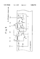
- FIG. 2 shows a main part of a semiconductor device for use in a first embodiment according to the present invention.
- a CMOS output buffer and a peripheral circuit thereof are shown in FIG. 2(a) and a cross sectional view of the CMOS output buffer is shown in FIG. 2(b).
- a CMOS output buffer 20 of the semiconductor device shown in FIG. 2 is constituted of a PMOS 21 which is a first MOS transistor and an NMOS 22 which is a second MOS transistor. These PMOS 21 and NMOS 22 are connected between a first power supply potential Vcc, for example 3.3v, and a ground potential Vss which is a second power supply potential.
- the source of the PMOS 21 is connected to the power supply potential Vcc and the source of the NMOS 22 is connected to the ground potential Vss.
- the drains of PMOS 21 and NMOS 22 are connected with each other and connected to an output terminal OUT.
- the gates of PMOS 21 and NMOS 22 are connected such that two outputs G1 an G2 of an output buffer control circuit 40 are entered therein.
- This semiconductor device is provided with an on-chip Vpp generating circuit 50 constituted, for example, of a typical booststrap circuit.
- the Vpp generating circuit 50 is connected between the power supply Vcc and the ground potential Vss and the third power supply potential Vpp generated by the Vpp generating circuit 50 is connected to the back gate of the PMOS 21.
- the Vpp generating circuit 50 has a function to output a power supply potential Vcc+ ⁇ ( ⁇ >0), for example 4 ⁇ 4.5v. That is, the output potential of the Vpp generating circuit 50 is escalated to a boosted potential Vcc+ ⁇ after the power supply is turned on, the boosted potential is maintained until the power supply is turned off and the back gate of the PMOS 21 is biased.
- the output buffer control circuit 40 functions to control the output buffer 20, for example, to supply signals G1 and G2, which correspond to the data read from a memory array of a DRAM, to the gates of PMOS 21 and NMOS 22.
- the output buffer 20, the output buffer control circuit 40 and the Vpp generating circuit 50 are formed on, for example, the P type substrate 1.
- the drain 21a and the source 21b of the PMOS 21 are formed in the N well 2 formed on the P type substrate 1 and the gate 21c of the PMOS 21 is formed between the drain 21a and the source 21b.
- the gate 22c of the NMOS 22 is formed between the drain 22a and the source 22b of the NMOS 22.
- the P type substrate 1 is biased to a negative voltage Vbb, for example -1.5v, to prevent a circuit between the P type substrate 1 and the N well 2 from being in a forward direction even though the input pin undershoots.
- data stored in a memory cell in the DRAM is read through a complementary bit line pair and a sense amplifier and supplied to the output buffer control circuit 40.
- the output buffer control circuit 40 outputs data signals G1 and G2 corresponding to the read data to the gates 21c and 22c of PMOS 21 and NMOS 22, respectively.
- the levels of the respective data signals G1 and G2 are the ground potential Vss
- the PMOS 21 turns on and the NMOS 22 turns off. Therefore, high level signals are output from the output terminal OUT.
- the levels of data signals G1 and G2 are the power supply potential Vcc
- the PMOS 21 turns off and the NMOS 22 turns on. Therefore low level signals are output from the output terminal OUT.
- the back gate bias of the PMOS 21 is set at a higher potential Vpp than the power supply potential Vcc and therefore the latch-up tolerance is improved.
- FIG. 3 is a cross sectional view of the CMOS output buffer shown in FIG. 1.
- FIG. 3 there are shown the N type well 2 formed on the P type substrate 1, the PMOS 21 constituted of the drain 21a, the source 21b and the gate 21c, the NMOS 22 constituted of the drain 22a, the source 22b and the gate 22c, the active region 24 in the N type well 2 to be connected to the bias potential Vpp, and the active region 25 in the substrate 1 to be connected to the bias potential Vbb.
- Parasitic bipolar transistors 31, 32, 33, 34 and 35 as shown in FIG. 3 are provided in the output buffer 20.
- Transistors 31 and 32 serve as n-p-n type bipolar transistors and transistors 33 to 35 serve as p-n-p type bipolar transistors.
- An ON voltage that is, a built-in potential of the bipolar transistors is assumed as BP and a threshold voltage of the PMOS 21 as Vtp. If a positive surge voltage from the output terminal OUT rises up to approximately Vcc+BP when the higher potential Vpp than the potential Vcc is Vpp ⁇ Vcc+(Vtp-BP), transistors 33 and 34 turn on before the PMOS 21 turns on. A current flowing through the transistor 34 flows to the side of the power supply Vcc and the current flowing through the transistor 33 flows into the substrate 1. In this case, the current flowing through the transistor 33 is larger than the current flowing through the transistor 34 since the potentials are different, and a greater part of the current flows in the substrate 1.
- a current supplying capacity of a bias potential Vbb generating circuit (not shown) is not so high because a stand-by current is controlled to be low. Therefore, when a current flowing into the substrate 1 due to the positive surge is compared with the current supplying capacity of the bias potential Vbb generating circuit, the current which flows into the substrate 1 is absolutely larger and, since the substrate resistance 36 is generally so large, the potential of the base of the transistor 31 steeply rises. Accordingly, when the current flows into the substrate 1, the potential Vbb of the substrate 1 steeply rises and the transistor 31 turns on.
- a trigger current flows in the path of the power supply Vcc ⁇ N type well resistor 37 ⁇ transistor 31 ⁇ ground potential Vss.
- the trigger current flows, a potential difference corresponding to the quantity of the trigger current is produced at both end points A and B of the N type well resistance 37, and the base potential of the transistor is lowered. Accordingly, the potential difference is produced between the base and the emitter of the transistor 35, and the transistor is turned on. Therefore, the current flows from the power supply potential Vcc to the substrate 1, and the potential Vbb of the substrate 1 rises again. Consequently, the current flows in the path of the power supply Vcc ⁇ N type well resistor 37 ⁇ transistor 31 ⁇ ground potential Vss, the potential difference between the points A and B further becomes large to finally result in the latch-up.
- the back gate bias of the PMOS 21 is the potential Vpp.
- the base potential of transistor becomes higher when the trigger current flows. In other words, the current which flows in the transistor 35 is controlled and the latch-up tolerance is improved.
- this embodiment enables to improve the latchup tolerance of the semiconductor device since the back gate bias of the PMOS 21 in the CMOS output buffer is set at the potential Vpp higher than the power supply potential Vcc. That is, the semiconductor device can be protected from damage due to the latch-up.
- FIGS. 4(a) and (b) are respectively a cross sectional view of the CMOS output buffer illustrating the second embodiment of the present invention and those element common to FIG. 2 are given the common symbols.
- This embodiment is a semiconductor device for which the construction of the output buffer 20 in the first embodiment is modified and the constructions of other components are as same as in FIG. 2.
- the drain 21a and the source 21b of the PMOS 21 are formed in the N type well 2 formed on the P type substrate 1 and the gate 21c of the PMOS 21 is formed between the drain 21a and the source 21b.
- the drain 22a and the source 22b of the NMOS 22 are formed on the P type substrate 1 and the gate of the NMOS 22 is formed between the drain 22a and the source 22b.
- the P type substrate 1 is biased to the negative voltage Vbb to prevent the P type substrate from being forward biased to the N type well.
- the active region 24 for setting the back gate bias of the PMOS 21 in FIG. 2 is replaced by active regions 26a and 26b.
- the active regions 26a and 26b are formed so as to surround the PMOS 21 on the edge of the N type well where the PMOS 21 is formed.
- FIG. 6 is an example of a plan view in FIG. 4 where the active region 26 is formed so as to completely surround the PMOS 21.
- the semiconductor device having this configuration operates as in the first embodiment.
- the data stored in the memory cells in, for example, the DRAM are read through the complementary bit line pair and the sense amplifier, and supplied to the output buffer control circuit 40.
- the output buffer control circuit 40 outputs data signals G1 and G2 corresponding to the read data to the gates 21c and 22c of PMOS 21 and NMOS 22, respectively. If both levels of data signals G1 and G2 are the ground potential Vss, the PMOS 21 turns on and the NMOS 22 turns off. Thus, a high level is output from the output terminal OUT. If both levels of data signals G1 and G2 are the power supply potential Vcc, the PMOS 21 turns off and the NMOS 22 turns on. Accordingly, a low level is output from the output terminal OUT.
- parasitic bipolar transistors 31 to 35 as shown in FIG. 4(b) are provided on the PMOS 21 and the NMOS 22, the back gate bias of the PMOS 21 is set at the potential Vpp higher than the power supply potential Vcc and the latch-up tolerance is improved as in the first embodiment.
- the active regions 26a and 26b are formed so as to surround the PMOS 21, the resistance values of the N type well resistors 38a and 38b are smaller than that of the N type well resistor 37 in the first embodiment. Therefore, the base potential of transistors 33 and 35 are stably maintained at approximately potential Vpp level. Consequently, the current which flows into the substrate 1 is reduced and the latch-up tolerance is improved as compared with that in the first embodiment.
- this embodiment enables to improve the latch-up tolerance of the semiconductor device as in the first embodiment since the back gate bias of the PMOS 21 in the CMOS output buffer 20 is set at the potential Vpp higher than the power supply potential Vcc. Since the active regions 26a and 26b for setting the back gate bias of the PMOS 21 are formed so as to surround the PMOS 21, the latch-up tolerance can be further improved.
- FIG. 6 shows the example where the active region 26 is formed so as to completely surround the PMOS 21, the active region 26 may be formed so as to substantially surround the PMOS 21.
- FIG. 7 shows another example of a plan view in FIG. 4 where the PMOS 21 is substantially surrounded by a diffusion layer to which the potential Vpp is supplied.
- FIG. 5 shows a main part of a semiconductor device according to a third embodiment of the present invention, and those elements common to FIG. 2 are given common symbols.
- the CMOS output buffer and the peripheral circuit are shown in FIG. 5(a) and the cross sectional view of the CMOS output buffer is shown in FIG. 5(b).
- the semiconductor device of this embodiment is provided with the output buffer control circuit 40 and the potential Vpp generating circuit 50 as in the first embodiment and an output buffer 60 different from the output buffer 20 is provided.
- the CMOS output buffer 60 of this semiconductor device has the PMOS 21 and the NMOS 22 connected in series between the power supply potential Vcc and the ground potential Vss as in FIG. 1 and further has a PMOS 61 which constitutes a third MOS transistor.
- the drain of the PMOS 61 is connected to the drains of the PMOS 21 and the NMOS 22 and the source thereof is connected to the power supply potential Vcc.
- the PMOS 61 is connected in parallel with the PMOS 21 between the power supply potential Vcc and the drain of the NMOS 22.
- the gate of the PMOS 61 is connected to the power supply potential Vcc and the back gate bias of the PMOS 61 is set at the potential Vpp.
- the PMOS 61 is provided and therefore a parasitic bipolar transistor as shown in FIG. 5(b) is formed in the N type well 2 in the CMOS output buffer 60. That is, the construction is such that parasitic bipolar transistors 71 to 73 are added to the parasitic bipolar transistors 31 to 35 shown in FIG. 3.
- the data stored in, for example, the memory cells in the DRAM are read through the complementary bit line pair and the sense amplifiers and supplied to the output buffer control circuit 40.
- the output buffer control circuit 40 outputs data signals G1 and G2 corresponding to the read data to the gates 21c and 22c of the PMOS 21 and the NMOS 22, respectively.
- the levels of data signals G1 and G2 are the ground potential Vss
- the PMOS 21 turns on and the NMOS 22 turns off. Therefore, the high level is output from the output terminal OUT.
- the levels of the respective data signals G1 and G2 are the power supply potential Vcc
- the PMOS 21 tuns off and the NMOS 22 turns on. Therefore, the low level is output from the output terminal OUT.
- the back gate bias of PMOS 21 and PMOS 61 is set at the potential Vpp higher than the power supply potential Vcc. Therefore, the latch-up tolerance is improved.
- a parasitic bipolar transistor 72 is disposed and, when the positive voltage surge is produced, the current separately flows into the bipolar transistor 34 and the bipolar transistor 72 and the current from the output terminal OUT flows to the side of the power supply potential Vcc. Accordingly, the current which flows into the substrate 1 reduces. In other words, the latch-up trigger current is suppressed. The latch-up tolerance is further improved. If the gate width of the PMOS 61 increases, the effect is further improved.
- the PMOS connected in parallel with the PMOS 21 in the CMOS output buffer is provided. Therefore, the latch-up trigger current can be suppressed and the latch-up tolerance of the semiconductor device can be improved.
- the semiconductor device which is the DRAM is described.
- the latch-up phenomenon is a problem in all semiconductor devices which receive the CMOS output buffer and various types of measures are required.
- the present invention is applicable to all these semiconductor devices and enables to improve the latch-up tolerance in a simple configuration without taking special measures.
- the back gate bias of the PMOS 21 is set at the potential Vpp higher than the power supply potential Vcc.
- the latch-up tolerance can similarly be improved better than the conventional one even when the back gate bias of the PMOS 21 is set at the power supply potential Vcc.
- the present invention is applicable even when it is set at the ground potential Vss.
- the bias of the N type well 2 is set to be higher than the potential Vcc and, therefore, an effect that the leak current from the PMOS 21 and the PMOS 61 can be reduced is expected.
- the first aspect of the invention is adapted so that the back gate bias of the first MOS transistor is set at the third power supply potential higher than the first power supply potential and therefore the base potential of the parasitic bipolar transistor disposed between the first MOS transistor and the substrate is higher than in the case that the back gate bias of the first MOS transistor is set at the first power supply potential. Accordingly, the current which flows in the parasitic transistor is suppressed and the latch-up tolerance in the semiconductor device can be improved.
- the active region for setting the back gate bias of the first MOS transistor is arranged so as to surround the first MOS transistor, the potential difference which occurs in the well resistor becomes small, the base potential of the parasitic bipolar transistor disposed between the first MOS transistor and the substrate becomes high, the current which flows in the parasitic bipolar transistor disposed between the first MOS transistor and the substrate is suppressed and the latch-up tolerance in the semiconductor device can be improved.
- the third aspect of the invention is adapted so that a third MOS transistor is provided in parallel with the first MOS transistor and the first power supply potential or a potential higher than the first power supply potential is applied to the back gate of the third MOS transistor. Therefore, when the surge voltage is produced at the output terminal, the current separately flows in the first power supply potential through the parasitic bipolar transistor disposed between the drain and the source of the first MOS transistor and the parasitic bipolar transistor disposed between the drain and the source of the third MOS transistor, and the latch-up trigger current can be suppressed. Therefore the latch-up tolerance of the semiconductor device is improved.
Abstract
Description
Claims (14)
Applications Claiming Priority (2)
| Application Number | Priority Date | Filing Date | Title |
|---|---|---|---|
| JP6-325573 | 1994-12-27 | ||
| JP6325573A JPH08181598A (en) | 1994-12-27 | 1994-12-27 | Semiconductor device |
Publications (1)
| Publication Number | Publication Date |
|---|---|
| US5686752A true US5686752A (en) | 1997-11-11 |
Family
ID=18178402
Family Applications (1)
| Application Number | Title | Priority Date | Filing Date |
|---|---|---|---|
| US08/576,614 Expired - Lifetime US5686752A (en) | 1994-12-27 | 1995-12-21 | Semiconductor device having a CMOS element as a buffer |
Country Status (6)
| Country | Link |
|---|---|
| US (1) | US5686752A (en) |
| EP (1) | EP0720295B1 (en) |
| JP (1) | JPH08181598A (en) |
| KR (1) | KR100318298B1 (en) |
| DE (1) | DE69522789T2 (en) |
| TW (1) | TW365085B (en) |
Cited By (11)
| Publication number | Priority date | Publication date | Assignee | Title |
|---|---|---|---|---|
| US5973554A (en) * | 1996-05-30 | 1999-10-26 | Mitsubishi Denki Kabushiki Kaisha | Semiconductor device structured to be less susceptible to power supply noise |
| US6150685A (en) * | 1997-11-13 | 2000-11-21 | Mitsubishi Denki Kabushiki Kaisha | Semiconductor device with filed-effect transistors of a complementary type and method of manufacturing the same |
| US6153914A (en) * | 1997-10-24 | 2000-11-28 | Stmicroelectronic S.R.L. | Output circuit for integrated circuits |
| US6228726B1 (en) | 2000-03-06 | 2001-05-08 | Taiwan Semiconductor Manufacturing Company | Method to suppress CMOS device latchup and improve interwell isolation |
| US6414360B1 (en) * | 1998-06-09 | 2002-07-02 | Aeroflex Utmc Microelectronic Systems, Inc. | Method of programmability and an architecture for cold sparing of CMOS arrays |
| US20050286295A1 (en) * | 2004-06-25 | 2005-12-29 | Kapre Ravindra M | Memory cell array latchup prevention |
| US20060202714A1 (en) * | 2004-12-07 | 2006-09-14 | Hoang Tim T | Apparatus and methods for adjusting performance characteristics and power consumption of programmable logic devices |
| US20080235541A1 (en) * | 2007-03-19 | 2008-09-25 | Powerchip Semiconductor Corp. | Method for testing a word line failure |
| US20110234742A1 (en) * | 2010-03-23 | 2011-09-29 | Oki Data Corporation | Drive device, print head and image forming apparatus |
| US9842629B2 (en) | 2004-06-25 | 2017-12-12 | Cypress Semiconductor Corporation | Memory cell array latchup prevention |
| US20190067281A1 (en) * | 2017-08-30 | 2019-02-28 | Taiwan Semiconductor Manufacturing Co., Ltd. | Semiconductor device and method for manufacturing the same |
Families Citing this family (7)
| Publication number | Priority date | Publication date | Assignee | Title |
|---|---|---|---|---|
| AU2001271166A1 (en) * | 2001-07-05 | 2002-01-08 | Telefonaktiebolaget Lm Ericsson (Publ) | Detrimental latch-up avoidance |
| JP2004207437A (en) * | 2002-12-25 | 2004-07-22 | Nec Corp | Ground switch circuit |
| US7330049B2 (en) * | 2006-03-06 | 2008-02-12 | Altera Corporation | Adjustable transistor body bias generation circuitry with latch-up prevention |
| JP5027471B2 (en) * | 2006-10-06 | 2012-09-19 | パナソニック株式会社 | Semiconductor integrated circuit device |
| JP5304505B2 (en) * | 2009-07-21 | 2013-10-02 | 富士通セミコンダクター株式会社 | Semiconductor integrated circuit |
| KR101153565B1 (en) | 2010-02-01 | 2012-06-12 | 한국과학기술원 | Radio frequency switch circuit |
| US8283979B2 (en) * | 2011-01-19 | 2012-10-09 | Harman International Industries, Incorporated | Amplifier system for a power converter |
Citations (5)
| Publication number | Priority date | Publication date | Assignee | Title |
|---|---|---|---|---|
| DE2632448A1 (en) * | 1975-07-18 | 1977-01-20 | Tokyo Shibaura Electric Co | Semiconductor device and process for its production |
| US5039877A (en) * | 1990-08-30 | 1991-08-13 | Micron Technology, Inc. | Low current substrate bias generator |
| JPH06177335A (en) * | 1992-12-07 | 1994-06-24 | Nippon Steel Corp | I/o circuit of integrated circuit |
| US5473183A (en) * | 1992-02-21 | 1995-12-05 | Sony Corporation | Semiconductor device of a first conductivity type which has a first well of a second conductivity type formed therein and a second well of the first conductivity type formed in the first well and a pair of MOSFET formed in the first and second wells |
| US5510630A (en) * | 1993-10-18 | 1996-04-23 | Westinghouse Electric Corporation | Non-volatile random access memory cell constructed of silicon carbide |
-
1994
- 1994-12-27 JP JP6325573A patent/JPH08181598A/en not_active Withdrawn
-
1995
- 1995-10-21 TW TW084111166A patent/TW365085B/en not_active IP Right Cessation
- 1995-12-13 DE DE69522789T patent/DE69522789T2/en not_active Expired - Lifetime
- 1995-12-13 EP EP95119653A patent/EP0720295B1/en not_active Expired - Lifetime
- 1995-12-21 US US08/576,614 patent/US5686752A/en not_active Expired - Lifetime
- 1995-12-27 KR KR1019950058776A patent/KR100318298B1/en not_active IP Right Cessation
Patent Citations (5)
| Publication number | Priority date | Publication date | Assignee | Title |
|---|---|---|---|---|
| DE2632448A1 (en) * | 1975-07-18 | 1977-01-20 | Tokyo Shibaura Electric Co | Semiconductor device and process for its production |
| US5039877A (en) * | 1990-08-30 | 1991-08-13 | Micron Technology, Inc. | Low current substrate bias generator |
| US5473183A (en) * | 1992-02-21 | 1995-12-05 | Sony Corporation | Semiconductor device of a first conductivity type which has a first well of a second conductivity type formed therein and a second well of the first conductivity type formed in the first well and a pair of MOSFET formed in the first and second wells |
| JPH06177335A (en) * | 1992-12-07 | 1994-06-24 | Nippon Steel Corp | I/o circuit of integrated circuit |
| US5510630A (en) * | 1993-10-18 | 1996-04-23 | Westinghouse Electric Corporation | Non-volatile random access memory cell constructed of silicon carbide |
Cited By (23)
| Publication number | Priority date | Publication date | Assignee | Title |
|---|---|---|---|---|
| US5973554A (en) * | 1996-05-30 | 1999-10-26 | Mitsubishi Denki Kabushiki Kaisha | Semiconductor device structured to be less susceptible to power supply noise |
| US6153914A (en) * | 1997-10-24 | 2000-11-28 | Stmicroelectronic S.R.L. | Output circuit for integrated circuits |
| US6150685A (en) * | 1997-11-13 | 2000-11-21 | Mitsubishi Denki Kabushiki Kaisha | Semiconductor device with filed-effect transistors of a complementary type and method of manufacturing the same |
| US6414360B1 (en) * | 1998-06-09 | 2002-07-02 | Aeroflex Utmc Microelectronic Systems, Inc. | Method of programmability and an architecture for cold sparing of CMOS arrays |
| US6228726B1 (en) | 2000-03-06 | 2001-05-08 | Taiwan Semiconductor Manufacturing Company | Method to suppress CMOS device latchup and improve interwell isolation |
| US8045410B2 (en) | 2004-06-25 | 2011-10-25 | Cypress Semiconductor Corporation | Memory cell array |
| US20050286295A1 (en) * | 2004-06-25 | 2005-12-29 | Kapre Ravindra M | Memory cell array latchup prevention |
| US9842629B2 (en) | 2004-06-25 | 2017-12-12 | Cypress Semiconductor Corporation | Memory cell array latchup prevention |
| US8837245B2 (en) | 2004-06-25 | 2014-09-16 | Cypress Semiconductor Corporation | Memory cell array latchup prevention |
| US20090213677A1 (en) * | 2004-06-25 | 2009-08-27 | Kapre Ravindra M | Memory Cell Array |
| US7773442B2 (en) * | 2004-06-25 | 2010-08-10 | Cypress Semiconductor Corporation | Memory cell array latchup prevention |
| US8493804B2 (en) | 2004-06-25 | 2013-07-23 | Cypress Semiconductor Corporation | Memory cell array latchup prevention |
| US7986160B2 (en) | 2004-12-07 | 2011-07-26 | Altera Corporation | Apparatus and methods for adjusting performance characteristics and power consumption of programmable logic devices |
| US20060202714A1 (en) * | 2004-12-07 | 2006-09-14 | Hoang Tim T | Apparatus and methods for adjusting performance characteristics and power consumption of programmable logic devices |
| US20080235541A1 (en) * | 2007-03-19 | 2008-09-25 | Powerchip Semiconductor Corp. | Method for testing a word line failure |
| US20110234742A1 (en) * | 2010-03-23 | 2011-09-29 | Oki Data Corporation | Drive device, print head and image forming apparatus |
| US8848012B2 (en) * | 2010-03-23 | 2014-09-30 | Oki Data Corporation | Drive device, print head and image forming apparatus |
| US20190067281A1 (en) * | 2017-08-30 | 2019-02-28 | Taiwan Semiconductor Manufacturing Co., Ltd. | Semiconductor device and method for manufacturing the same |
| US10366992B2 (en) * | 2017-08-30 | 2019-07-30 | Taiwan Semiconductor Manufacturing Co., Ltd. | Semiconductor device including transistors sharing gates |
| US11222893B2 (en) | 2017-08-30 | 2022-01-11 | Taiwan Semiconductor Manufacturing Co., Ltd. | Semiconductor device including transistors sharing gates with structures having reduced parasitic circuit |
| US20220130825A1 (en) * | 2017-08-30 | 2022-04-28 | Taiwan Semiconductor Manufacturing Co., Ltd. | Semiconductor device including transistors sharing gates with structures having reduced parasitic circuit |
| US11855088B2 (en) * | 2017-08-30 | 2023-12-26 | Taiwan Semiconductor Manufacturing Co., Ltd. | Semiconductor device including transistors sharing gates with structures having reduced parasitic circuit |
| US11908859B2 (en) | 2017-08-30 | 2024-02-20 | Taiwan Semiconductor Manufacturing Co., Ltd. | Semiconductor device including transistors sharing gates with structures having reduced parasitic circuit |
Also Published As
| Publication number | Publication date |
|---|---|
| EP0720295A2 (en) | 1996-07-03 |
| KR100318298B1 (en) | 2002-04-22 |
| TW365085B (en) | 1999-07-21 |
| EP0720295B1 (en) | 2001-09-19 |
| EP0720295A3 (en) | 1997-02-05 |
| DE69522789T2 (en) | 2002-05-23 |
| JPH08181598A (en) | 1996-07-12 |
| DE69522789D1 (en) | 2001-10-25 |
Similar Documents
| Publication | Publication Date | Title |
|---|---|---|
| US5686752A (en) | Semiconductor device having a CMOS element as a buffer | |
| KR940001251B1 (en) | Voltage control circuit | |
| KR960003374B1 (en) | Semiconductor integrated circuit device | |
| EP0090116B1 (en) | Cmis semiconductor device with two power supplies | |
| KR0155078B1 (en) | Semiconductor circuit having cmos circuit for use in strong electric field | |
| KR900004725B1 (en) | Power voltage regulator circuit | |
| KR0132053B1 (en) | Semiconductor integrated circuit device and its composite electronic device | |
| US5867042A (en) | Switch for minimizing transistor exposure to high voltage | |
| US5942784A (en) | Semiconductor device | |
| US5963061A (en) | Switch for minimizing transistor exposure to high voltage | |
| US4260909A (en) | Back gate bias voltage generator circuit | |
| JPH0323999B2 (en) | ||
| US6144080A (en) | Semiconductor integrated circuit device having field shield MOS devices | |
| JP3105512B2 (en) | MOS type semiconductor integrated circuit | |
| JP3875285B2 (en) | Intermediate voltage generation circuit for semiconductor integrated circuit | |
| US4904885A (en) | Substrate bias circuit having substrate bias voltage clamp and operating method therefor | |
| US6476641B2 (en) | Low power consuming circuit | |
| US5986309A (en) | Semiconductor integrated circuit apparatus having a plurality of well bias voltage supply circuits | |
| US6271692B1 (en) | Semiconductor integrated circuit | |
| JP2799772B2 (en) | Low standby current intermediate DC voltage generator | |
| US6885232B2 (en) | Semiconductor integrated circuit having a function determination circuit | |
| US6172554B1 (en) | Power supply insensitive substrate bias voltage detector circuit | |
| JPS6155195B2 (en) | ||
| US5875089A (en) | Input protection circuit device | |
| KR950002275B1 (en) | Semiconductor integrated circuit including p-channel mos transistors having different threshold voltages |
Legal Events
| Date | Code | Title | Description |
|---|---|---|---|
| AS | Assignment |
Owner name: DEFENSE, DEPARTMENT OF, UNITED STATES, AS REPRESEN Free format text: CONFIRMATORY LICENSE;ASSIGNOR:MENTOR GRAPHICS CORPORATION;REEL/FRAME:008090/0929 Effective date: 19960515 |
|
| STCF | Information on status: patent grant |
Free format text: PATENTED CASE |
|
| FEPP | Fee payment procedure |
Free format text: PAYOR NUMBER ASSIGNED (ORIGINAL EVENT CODE: ASPN); ENTITY STATUS OF PATENT OWNER: LARGE ENTITY |
|
| FPAY | Fee payment |
Year of fee payment: 4 |
|
| FPAY | Fee payment |
Year of fee payment: 8 |
|
| AS | Assignment |
Owner name: OKI SEMICONDUCTOR CO., LTD., JAPAN Free format text: CHANGE OF NAME;ASSIGNOR:OKI ELECTRIC INDUSTRY CO., LTD.;REEL/FRAME:022288/0277 Effective date: 20081001 |
|
| FPAY | Fee payment |
Year of fee payment: 12 |
|
| AS | Assignment |
Owner name: LAPIS SEMICONDUCTOR CO., LTD., JAPAN Free format text: CHANGE OF NAME;ASSIGNOR:OKI SEMICONDUCTOR CO., LTD;REEL/FRAME:032495/0483 Effective date: 20111003 |