US5695568A - Chemical vapor deposition chamber - Google Patents
Chemical vapor deposition chamber Download PDFInfo
- Publication number
- US5695568A US5695568A US08/200,862 US20086294A US5695568A US 5695568 A US5695568 A US 5695568A US 20086294 A US20086294 A US 20086294A US 5695568 A US5695568 A US 5695568A
- Authority
- US
- United States
- Prior art keywords
- substrate
- enclosure
- support member
- stem
- substrate support
- Prior art date
- Legal status (The legal status is an assumption and is not a legal conclusion. Google has not performed a legal analysis and makes no representation as to the accuracy of the status listed.)
- Expired - Lifetime
Links
Images


Classifications
-
- C—CHEMISTRY; METALLURGY
- C23—COATING METALLIC MATERIAL; COATING MATERIAL WITH METALLIC MATERIAL; CHEMICAL SURFACE TREATMENT; DIFFUSION TREATMENT OF METALLIC MATERIAL; COATING BY VACUUM EVAPORATION, BY SPUTTERING, BY ION IMPLANTATION OR BY CHEMICAL VAPOUR DEPOSITION, IN GENERAL; INHIBITING CORROSION OF METALLIC MATERIAL OR INCRUSTATION IN GENERAL
- C23C—COATING METALLIC MATERIAL; COATING MATERIAL WITH METALLIC MATERIAL; SURFACE TREATMENT OF METALLIC MATERIAL BY DIFFUSION INTO THE SURFACE, BY CHEMICAL CONVERSION OR SUBSTITUTION; COATING BY VACUUM EVAPORATION, BY SPUTTERING, BY ION IMPLANTATION OR BY CHEMICAL VAPOUR DEPOSITION, IN GENERAL
- C23C16/00—Chemical coating by decomposition of gaseous compounds, without leaving reaction products of surface material in the coating, i.e. chemical vapour deposition [CVD] processes
- C23C16/44—Chemical coating by decomposition of gaseous compounds, without leaving reaction products of surface material in the coating, i.e. chemical vapour deposition [CVD] processes characterised by the method of coating
- C23C16/455—Chemical coating by decomposition of gaseous compounds, without leaving reaction products of surface material in the coating, i.e. chemical vapour deposition [CVD] processes characterised by the method of coating characterised by the method used for introducing gases into reaction chamber or for modifying gas flows in reaction chamber
- C23C16/45519—Inert gas curtains
-
- C—CHEMISTRY; METALLURGY
- C23—COATING METALLIC MATERIAL; COATING MATERIAL WITH METALLIC MATERIAL; CHEMICAL SURFACE TREATMENT; DIFFUSION TREATMENT OF METALLIC MATERIAL; COATING BY VACUUM EVAPORATION, BY SPUTTERING, BY ION IMPLANTATION OR BY CHEMICAL VAPOUR DEPOSITION, IN GENERAL; INHIBITING CORROSION OF METALLIC MATERIAL OR INCRUSTATION IN GENERAL
- C23C—COATING METALLIC MATERIAL; COATING MATERIAL WITH METALLIC MATERIAL; SURFACE TREATMENT OF METALLIC MATERIAL BY DIFFUSION INTO THE SURFACE, BY CHEMICAL CONVERSION OR SUBSTITUTION; COATING BY VACUUM EVAPORATION, BY SPUTTERING, BY ION IMPLANTATION OR BY CHEMICAL VAPOUR DEPOSITION, IN GENERAL
- C23C16/00—Chemical coating by decomposition of gaseous compounds, without leaving reaction products of surface material in the coating, i.e. chemical vapour deposition [CVD] processes
- C23C16/44—Chemical coating by decomposition of gaseous compounds, without leaving reaction products of surface material in the coating, i.e. chemical vapour deposition [CVD] processes characterised by the method of coating
- C23C16/4412—Details relating to the exhausts, e.g. pumps, filters, scrubbers, particle traps
-
- C—CHEMISTRY; METALLURGY
- C23—COATING METALLIC MATERIAL; COATING MATERIAL WITH METALLIC MATERIAL; CHEMICAL SURFACE TREATMENT; DIFFUSION TREATMENT OF METALLIC MATERIAL; COATING BY VACUUM EVAPORATION, BY SPUTTERING, BY ION IMPLANTATION OR BY CHEMICAL VAPOUR DEPOSITION, IN GENERAL; INHIBITING CORROSION OF METALLIC MATERIAL OR INCRUSTATION IN GENERAL
- C23C—COATING METALLIC MATERIAL; COATING MATERIAL WITH METALLIC MATERIAL; SURFACE TREATMENT OF METALLIC MATERIAL BY DIFFUSION INTO THE SURFACE, BY CHEMICAL CONVERSION OR SUBSTITUTION; COATING BY VACUUM EVAPORATION, BY SPUTTERING, BY ION IMPLANTATION OR BY CHEMICAL VAPOUR DEPOSITION, IN GENERAL
- C23C16/00—Chemical coating by decomposition of gaseous compounds, without leaving reaction products of surface material in the coating, i.e. chemical vapour deposition [CVD] processes
- C23C16/44—Chemical coating by decomposition of gaseous compounds, without leaving reaction products of surface material in the coating, i.e. chemical vapour deposition [CVD] processes characterised by the method of coating
- C23C16/455—Chemical coating by decomposition of gaseous compounds, without leaving reaction products of surface material in the coating, i.e. chemical vapour deposition [CVD] processes characterised by the method of coating characterised by the method used for introducing gases into reaction chamber or for modifying gas flows in reaction chamber
- C23C16/45519—Inert gas curtains
- C23C16/45521—Inert gas curtains the gas, other than thermal contact gas, being introduced the rear of the substrate to flow around its periphery
-
- C—CHEMISTRY; METALLURGY
- C23—COATING METALLIC MATERIAL; COATING MATERIAL WITH METALLIC MATERIAL; CHEMICAL SURFACE TREATMENT; DIFFUSION TREATMENT OF METALLIC MATERIAL; COATING BY VACUUM EVAPORATION, BY SPUTTERING, BY ION IMPLANTATION OR BY CHEMICAL VAPOUR DEPOSITION, IN GENERAL; INHIBITING CORROSION OF METALLIC MATERIAL OR INCRUSTATION IN GENERAL
- C23C—COATING METALLIC MATERIAL; COATING MATERIAL WITH METALLIC MATERIAL; SURFACE TREATMENT OF METALLIC MATERIAL BY DIFFUSION INTO THE SURFACE, BY CHEMICAL CONVERSION OR SUBSTITUTION; COATING BY VACUUM EVAPORATION, BY SPUTTERING, BY ION IMPLANTATION OR BY CHEMICAL VAPOUR DEPOSITION, IN GENERAL
- C23C16/00—Chemical coating by decomposition of gaseous compounds, without leaving reaction products of surface material in the coating, i.e. chemical vapour deposition [CVD] processes
- C23C16/44—Chemical coating by decomposition of gaseous compounds, without leaving reaction products of surface material in the coating, i.e. chemical vapour deposition [CVD] processes characterised by the method of coating
- C23C16/458—Chemical coating by decomposition of gaseous compounds, without leaving reaction products of surface material in the coating, i.e. chemical vapour deposition [CVD] processes characterised by the method of coating characterised by the method used for supporting substrates in the reaction chamber
- C23C16/4582—Rigid and flat substrates, e.g. plates or discs
- C23C16/4583—Rigid and flat substrates, e.g. plates or discs the substrate being supported substantially horizontally
- C23C16/4585—Devices at or outside the perimeter of the substrate support, e.g. clamping rings, shrouds
-
- C—CHEMISTRY; METALLURGY
- C23—COATING METALLIC MATERIAL; COATING MATERIAL WITH METALLIC MATERIAL; CHEMICAL SURFACE TREATMENT; DIFFUSION TREATMENT OF METALLIC MATERIAL; COATING BY VACUUM EVAPORATION, BY SPUTTERING, BY ION IMPLANTATION OR BY CHEMICAL VAPOUR DEPOSITION, IN GENERAL; INHIBITING CORROSION OF METALLIC MATERIAL OR INCRUSTATION IN GENERAL
- C23C—COATING METALLIC MATERIAL; COATING MATERIAL WITH METALLIC MATERIAL; SURFACE TREATMENT OF METALLIC MATERIAL BY DIFFUSION INTO THE SURFACE, BY CHEMICAL CONVERSION OR SUBSTITUTION; COATING BY VACUUM EVAPORATION, BY SPUTTERING, BY ION IMPLANTATION OR BY CHEMICAL VAPOUR DEPOSITION, IN GENERAL
- C23C16/00—Chemical coating by decomposition of gaseous compounds, without leaving reaction products of surface material in the coating, i.e. chemical vapour deposition [CVD] processes
- C23C16/44—Chemical coating by decomposition of gaseous compounds, without leaving reaction products of surface material in the coating, i.e. chemical vapour deposition [CVD] processes characterised by the method of coating
- C23C16/46—Chemical coating by decomposition of gaseous compounds, without leaving reaction products of surface material in the coating, i.e. chemical vapour deposition [CVD] processes characterised by the method of coating characterised by the method used for heating the substrate
-
- H—ELECTRICITY
- H01—ELECTRIC ELEMENTS
- H01L—SEMICONDUCTOR DEVICES NOT COVERED BY CLASS H10
- H01L21/00—Processes or apparatus adapted for the manufacture or treatment of semiconductor or solid state devices or of parts thereof
- H01L21/67—Apparatus specially adapted for handling semiconductor or electric solid state devices during manufacture or treatment thereof; Apparatus specially adapted for handling wafers during manufacture or treatment of semiconductor or electric solid state devices or components ; Apparatus not specifically provided for elsewhere
- H01L21/67005—Apparatus not specifically provided for elsewhere
- H01L21/67011—Apparatus for manufacture or treatment
- H01L21/67098—Apparatus for thermal treatment
- H01L21/67103—Apparatus for thermal treatment mainly by conduction
-
- H—ELECTRICITY
- H01—ELECTRIC ELEMENTS
- H01L—SEMICONDUCTOR DEVICES NOT COVERED BY CLASS H10
- H01L21/00—Processes or apparatus adapted for the manufacture or treatment of semiconductor or solid state devices or of parts thereof
- H01L21/67—Apparatus specially adapted for handling semiconductor or electric solid state devices during manufacture or treatment thereof; Apparatus specially adapted for handling wafers during manufacture or treatment of semiconductor or electric solid state devices or components ; Apparatus not specifically provided for elsewhere
- H01L21/68—Apparatus specially adapted for handling semiconductor or electric solid state devices during manufacture or treatment thereof; Apparatus specially adapted for handling wafers during manufacture or treatment of semiconductor or electric solid state devices or components ; Apparatus not specifically provided for elsewhere for positioning, orientation or alignment
-
- H—ELECTRICITY
- H01—ELECTRIC ELEMENTS
- H01L—SEMICONDUCTOR DEVICES NOT COVERED BY CLASS H10
- H01L21/00—Processes or apparatus adapted for the manufacture or treatment of semiconductor or solid state devices or of parts thereof
- H01L21/67—Apparatus specially adapted for handling semiconductor or electric solid state devices during manufacture or treatment thereof; Apparatus specially adapted for handling wafers during manufacture or treatment of semiconductor or electric solid state devices or components ; Apparatus not specifically provided for elsewhere
- H01L21/683—Apparatus specially adapted for handling semiconductor or electric solid state devices during manufacture or treatment thereof; Apparatus specially adapted for handling wafers during manufacture or treatment of semiconductor or electric solid state devices or components ; Apparatus not specifically provided for elsewhere for supporting or gripping
- H01L21/687—Apparatus specially adapted for handling semiconductor or electric solid state devices during manufacture or treatment thereof; Apparatus specially adapted for handling wafers during manufacture or treatment of semiconductor or electric solid state devices or components ; Apparatus not specifically provided for elsewhere for supporting or gripping using mechanical means, e.g. chucks, clamps or pinches
- H01L21/68714—Apparatus specially adapted for handling semiconductor or electric solid state devices during manufacture or treatment thereof; Apparatus specially adapted for handling wafers during manufacture or treatment of semiconductor or electric solid state devices or components ; Apparatus not specifically provided for elsewhere for supporting or gripping using mechanical means, e.g. chucks, clamps or pinches the wafers being placed on a susceptor, stage or support
- H01L21/68721—Apparatus specially adapted for handling semiconductor or electric solid state devices during manufacture or treatment thereof; Apparatus specially adapted for handling wafers during manufacture or treatment of semiconductor or electric solid state devices or components ; Apparatus not specifically provided for elsewhere for supporting or gripping using mechanical means, e.g. chucks, clamps or pinches the wafers being placed on a susceptor, stage or support characterised by edge clamping, e.g. clamping ring
-
- H—ELECTRICITY
- H01—ELECTRIC ELEMENTS
- H01L—SEMICONDUCTOR DEVICES NOT COVERED BY CLASS H10
- H01L21/00—Processes or apparatus adapted for the manufacture or treatment of semiconductor or solid state devices or of parts thereof
- H01L21/67—Apparatus specially adapted for handling semiconductor or electric solid state devices during manufacture or treatment thereof; Apparatus specially adapted for handling wafers during manufacture or treatment of semiconductor or electric solid state devices or components ; Apparatus not specifically provided for elsewhere
- H01L21/683—Apparatus specially adapted for handling semiconductor or electric solid state devices during manufacture or treatment thereof; Apparatus specially adapted for handling wafers during manufacture or treatment of semiconductor or electric solid state devices or components ; Apparatus not specifically provided for elsewhere for supporting or gripping
- H01L21/687—Apparatus specially adapted for handling semiconductor or electric solid state devices during manufacture or treatment thereof; Apparatus specially adapted for handling wafers during manufacture or treatment of semiconductor or electric solid state devices or components ; Apparatus not specifically provided for elsewhere for supporting or gripping using mechanical means, e.g. chucks, clamps or pinches
- H01L21/68714—Apparatus specially adapted for handling semiconductor or electric solid state devices during manufacture or treatment thereof; Apparatus specially adapted for handling wafers during manufacture or treatment of semiconductor or electric solid state devices or components ; Apparatus not specifically provided for elsewhere for supporting or gripping using mechanical means, e.g. chucks, clamps or pinches the wafers being placed on a susceptor, stage or support
- H01L21/68728—Apparatus specially adapted for handling semiconductor or electric solid state devices during manufacture or treatment thereof; Apparatus specially adapted for handling wafers during manufacture or treatment of semiconductor or electric solid state devices or components ; Apparatus not specifically provided for elsewhere for supporting or gripping using mechanical means, e.g. chucks, clamps or pinches the wafers being placed on a susceptor, stage or support characterised by a plurality of separate clamping members, e.g. clamping fingers
-
- H—ELECTRICITY
- H01—ELECTRIC ELEMENTS
- H01L—SEMICONDUCTOR DEVICES NOT COVERED BY CLASS H10
- H01L21/00—Processes or apparatus adapted for the manufacture or treatment of semiconductor or solid state devices or of parts thereof
- H01L21/67—Apparatus specially adapted for handling semiconductor or electric solid state devices during manufacture or treatment thereof; Apparatus specially adapted for handling wafers during manufacture or treatment of semiconductor or electric solid state devices or components ; Apparatus not specifically provided for elsewhere
- H01L21/683—Apparatus specially adapted for handling semiconductor or electric solid state devices during manufacture or treatment thereof; Apparatus specially adapted for handling wafers during manufacture or treatment of semiconductor or electric solid state devices or components ; Apparatus not specifically provided for elsewhere for supporting or gripping
- H01L21/687—Apparatus specially adapted for handling semiconductor or electric solid state devices during manufacture or treatment thereof; Apparatus specially adapted for handling wafers during manufacture or treatment of semiconductor or electric solid state devices or components ; Apparatus not specifically provided for elsewhere for supporting or gripping using mechanical means, e.g. chucks, clamps or pinches
- H01L21/68714—Apparatus specially adapted for handling semiconductor or electric solid state devices during manufacture or treatment thereof; Apparatus specially adapted for handling wafers during manufacture or treatment of semiconductor or electric solid state devices or components ; Apparatus not specifically provided for elsewhere for supporting or gripping using mechanical means, e.g. chucks, clamps or pinches the wafers being placed on a susceptor, stage or support
- H01L21/68735—Apparatus specially adapted for handling semiconductor or electric solid state devices during manufacture or treatment thereof; Apparatus specially adapted for handling wafers during manufacture or treatment of semiconductor or electric solid state devices or components ; Apparatus not specifically provided for elsewhere for supporting or gripping using mechanical means, e.g. chucks, clamps or pinches the wafers being placed on a susceptor, stage or support characterised by edge profile or support profile
-
- H—ELECTRICITY
- H01—ELECTRIC ELEMENTS
- H01L—SEMICONDUCTOR DEVICES NOT COVERED BY CLASS H10
- H01L21/00—Processes or apparatus adapted for the manufacture or treatment of semiconductor or solid state devices or of parts thereof
- H01L21/67—Apparatus specially adapted for handling semiconductor or electric solid state devices during manufacture or treatment thereof; Apparatus specially adapted for handling wafers during manufacture or treatment of semiconductor or electric solid state devices or components ; Apparatus not specifically provided for elsewhere
- H01L21/683—Apparatus specially adapted for handling semiconductor or electric solid state devices during manufacture or treatment thereof; Apparatus specially adapted for handling wafers during manufacture or treatment of semiconductor or electric solid state devices or components ; Apparatus not specifically provided for elsewhere for supporting or gripping
- H01L21/687—Apparatus specially adapted for handling semiconductor or electric solid state devices during manufacture or treatment thereof; Apparatus specially adapted for handling wafers during manufacture or treatment of semiconductor or electric solid state devices or components ; Apparatus not specifically provided for elsewhere for supporting or gripping using mechanical means, e.g. chucks, clamps or pinches
- H01L21/68714—Apparatus specially adapted for handling semiconductor or electric solid state devices during manufacture or treatment thereof; Apparatus specially adapted for handling wafers during manufacture or treatment of semiconductor or electric solid state devices or components ; Apparatus not specifically provided for elsewhere for supporting or gripping using mechanical means, e.g. chucks, clamps or pinches the wafers being placed on a susceptor, stage or support
- H01L21/6875—Apparatus specially adapted for handling semiconductor or electric solid state devices during manufacture or treatment thereof; Apparatus specially adapted for handling wafers during manufacture or treatment of semiconductor or electric solid state devices or components ; Apparatus not specifically provided for elsewhere for supporting or gripping using mechanical means, e.g. chucks, clamps or pinches the wafers being placed on a susceptor, stage or support characterised by a plurality of individual support members, e.g. support posts or protrusions
-
- H—ELECTRICITY
- H01—ELECTRIC ELEMENTS
- H01L—SEMICONDUCTOR DEVICES NOT COVERED BY CLASS H10
- H01L21/00—Processes or apparatus adapted for the manufacture or treatment of semiconductor or solid state devices or of parts thereof
- H01L21/67—Apparatus specially adapted for handling semiconductor or electric solid state devices during manufacture or treatment thereof; Apparatus specially adapted for handling wafers during manufacture or treatment of semiconductor or electric solid state devices or components ; Apparatus not specifically provided for elsewhere
- H01L21/683—Apparatus specially adapted for handling semiconductor or electric solid state devices during manufacture or treatment thereof; Apparatus specially adapted for handling wafers during manufacture or treatment of semiconductor or electric solid state devices or components ; Apparatus not specifically provided for elsewhere for supporting or gripping
- H01L21/687—Apparatus specially adapted for handling semiconductor or electric solid state devices during manufacture or treatment thereof; Apparatus specially adapted for handling wafers during manufacture or treatment of semiconductor or electric solid state devices or components ; Apparatus not specifically provided for elsewhere for supporting or gripping using mechanical means, e.g. chucks, clamps or pinches
- H01L21/68714—Apparatus specially adapted for handling semiconductor or electric solid state devices during manufacture or treatment thereof; Apparatus specially adapted for handling wafers during manufacture or treatment of semiconductor or electric solid state devices or components ; Apparatus not specifically provided for elsewhere for supporting or gripping using mechanical means, e.g. chucks, clamps or pinches the wafers being placed on a susceptor, stage or support
- H01L21/68785—Apparatus specially adapted for handling semiconductor or electric solid state devices during manufacture or treatment thereof; Apparatus specially adapted for handling wafers during manufacture or treatment of semiconductor or electric solid state devices or components ; Apparatus not specifically provided for elsewhere for supporting or gripping using mechanical means, e.g. chucks, clamps or pinches the wafers being placed on a susceptor, stage or support characterised by the mechanical construction of the susceptor, stage or support
-
- H—ELECTRICITY
- H01—ELECTRIC ELEMENTS
- H01L—SEMICONDUCTOR DEVICES NOT COVERED BY CLASS H10
- H01L21/00—Processes or apparatus adapted for the manufacture or treatment of semiconductor or solid state devices or of parts thereof
- H01L21/67—Apparatus specially adapted for handling semiconductor or electric solid state devices during manufacture or treatment thereof; Apparatus specially adapted for handling wafers during manufacture or treatment of semiconductor or electric solid state devices or components ; Apparatus not specifically provided for elsewhere
- H01L21/683—Apparatus specially adapted for handling semiconductor or electric solid state devices during manufacture or treatment thereof; Apparatus specially adapted for handling wafers during manufacture or treatment of semiconductor or electric solid state devices or components ; Apparatus not specifically provided for elsewhere for supporting or gripping
- H01L21/687—Apparatus specially adapted for handling semiconductor or electric solid state devices during manufacture or treatment thereof; Apparatus specially adapted for handling wafers during manufacture or treatment of semiconductor or electric solid state devices or components ; Apparatus not specifically provided for elsewhere for supporting or gripping using mechanical means, e.g. chucks, clamps or pinches
- H01L21/68714—Apparatus specially adapted for handling semiconductor or electric solid state devices during manufacture or treatment thereof; Apparatus specially adapted for handling wafers during manufacture or treatment of semiconductor or electric solid state devices or components ; Apparatus not specifically provided for elsewhere for supporting or gripping using mechanical means, e.g. chucks, clamps or pinches the wafers being placed on a susceptor, stage or support
- H01L21/68792—Apparatus specially adapted for handling semiconductor or electric solid state devices during manufacture or treatment thereof; Apparatus specially adapted for handling wafers during manufacture or treatment of semiconductor or electric solid state devices or components ; Apparatus not specifically provided for elsewhere for supporting or gripping using mechanical means, e.g. chucks, clamps or pinches the wafers being placed on a susceptor, stage or support characterised by the construction of the shaft
-
- Y—GENERAL TAGGING OF NEW TECHNOLOGICAL DEVELOPMENTS; GENERAL TAGGING OF CROSS-SECTIONAL TECHNOLOGIES SPANNING OVER SEVERAL SECTIONS OF THE IPC; TECHNICAL SUBJECTS COVERED BY FORMER USPC CROSS-REFERENCE ART COLLECTIONS [XRACs] AND DIGESTS
- Y10—TECHNICAL SUBJECTS COVERED BY FORMER USPC
- Y10S—TECHNICAL SUBJECTS COVERED BY FORMER USPC CROSS-REFERENCE ART COLLECTIONS [XRACs] AND DIGESTS
- Y10S438/00—Semiconductor device manufacturing: process
- Y10S438/935—Gas flow control
Definitions
- the present invention relates to methods and apparatus for depositing useful layers of materials on substrates used in the manufacture of semiconductor die. More particularly, the invention relates to improved apparatus and methods for use in the processing of substrates, such as by chemical vapor deposition.
- Chemical vapor deposition commonly referred to as "CVD," is used to deposit a thin layer of material on a semiconductor substrate.
- a vacuum chamber is provided with a susceptor configured to receive a substrate thereon.
- the substrate is placed into and removed from the chamber by a robot blade.
- the chamber includes an intermediate substrate positioning assembly on which the substrate is located when it is placed into, or about to be removed from, the chamber.
- the susceptor is passed through the center of the substrate positioning assembly to lift the substrate therefrom. The susceptor and the substrate are then heated to a temperature of between 250°-650° C.
- a precursor gas is charged to the vacuum chamber through a gas manifold situated above the substrate.
- the precursor gas reacts with the heated substrate surface to deposit the thin material layer thereon.
- volatile byproduct gasses are formed, and these gasses are pumped out of the vacuum chamber through a chamber exhaust system.
- a primary goal of substrate processing is to obtain as many useful die as possible from each substrate.
- Many factors influence the processing of substrates in the CVD chamber and affect the ultimate yield of die from each substrate processed therein. These factors include processing variables, which affect the uniformity and thickness of the deposition material layer deposited on the substrate, and contaminants that can attach to the substrate and contaminate one or more die therein. Both of these factors must be controlled in CVD and other processes to maximize the die yield from each substrate.
- the exhaust system of the chamber includes a circumferential exhaust channel located above the substrate adjacent the perimeter thereof, through which the reacted process gas is vented.
- a gap exists in the circumferential exhaust channel where the slit valve for moving the substrate into and out of the chamber passes through the chamber wall. The exhausting of reacted gaseous products from the chamber is less efficient near this gap, and thus the exhausting of reaction products is non-uniform in the chamber.
- CVD processing chambers include multiple sources of particle contaminants which, if received on the substrate, reduce the die yield therefrom.
- One primary source of particulate contamination in CVD processing is the deposition material deposited on the chamber surfaces during processing.
- a material layer is indiscriminately deposited on all surfaces within the chamber which are contacted with the gas, such as lamp covers. If these chamber surfaces are later touched or rubbed, or if the material layer is loosely attached to the chamber surface and the chamber is shaken or vibrated, particles of deposition material layer can become free in the chamber and contaminate the substrate.
- the deposition material layer does not typically firmly attach itself to the edge and underside of the substrate, and the layer formed in that location of the substrate is known to flake off the substrate and become a particle contaminant.
- a shadow ring is a masking member, which is received on the susceptor and contacts the upper, outer, circumferential area of the substrate and limits access of the deposition gas to the contacted area of the substrate.
- the shadow ring has several limitations which contribute to the non-uniform processing of substrates. The volatile deposition gas still tends to migrate under the lip of the shadow ring and deposit a material layer on the substrate edge and underside which may later flake off. Additionally, the engagement of the shadow ring with the substrate can create particles.
- the shadow ring is a heat sink, which draws heat out of the substrate and thus reduces the temperature of the substrate adjacent the area of contact between the substrate and shadow ring, which affects the thickness of the deposition material layer on the area of the substrate adjacent the shadow ring.
- EPO 467 623 A3 One alternative to the shadow ring is disclosed in European Patent Application No. EPO 467 623 A3, published Jan. 22, 1992.
- a shroud is provided around the perimeter of the substrate.
- the shroud includes a lip which overhangs, but does not touch, the substrate.
- a gas is provided to the underside of the substrate, and a portion of this gas flows outwardly between the substrate and susceptor and into a gap formed between the substrate and the shroud.
- the shroud creates a circumferential channel in which a non-reactive gas may be maintained to mask the edge of the substrate, the structure shown in EPO 467 623 A3 has several disadvantages.
- the shroud when the shroud is received on the susceptor, it aligns with the susceptor and no means is disclosed for aligning the substrate with the shroud. Any substantial misalignment between the substrate and the susceptor will result in substantial misalignment between the shroud and substrate, and the resulting annular gap between the substrate and shroud will be non-uniform around the perimeter of the substrate. This will create differential masking gas flow in different locations of the substrate edge. Second, introduction of the masking gas inwardly of the outer diameter of the substrate can cause the substrate to float off the susceptor during processing if the chamber pressure and process gas flow are not closely controlled. Finally, the European application notes that the shroud disclosed therein masks the upper surface of the substrate and prevents depositions thereon, which reduces the useful area of the substrate.
- a further source of substrate particulate contamination occurs where a cracked, warped or substantially misaligned substrate is present in the chamber. If a cracked, warped or substantially misaligned substrate is encountered, substantial numbers of particulate contaminants can be generated as the substrate is moved in the chamber. Additionally, if large segments of the substrate become free in the chamber, they may seriously damage the chamber components. Finally, the upper surface and passageways of the susceptor could be exposed to the corrosive reactive gas if a cracked, warped or misaligned substrate is processed in the chamber.
- the present invention is useful as a CVD processing apparatus for depositing blanket and selectively deposited tungsten, tungsten silicide, titanium nitride and other deposition materials with improved uniformity and controllability.
- the invention includes multiple embodiments which may be used independently or concurrently to improve the control of processing variables and/or reduce the incidence of contamination of the substrate during processing. Although the embodiments of the invention are discussed with reference to a CVD chamber, the embodiments of the invention are applicable to other substrate processes and process environments.
- the apparatus includes a chamber having a substrate support member on which the substrate is located for processing.
- the substrate is positioned on the substrate support member with a positioning means, which positions the substrate above the support member for insertion and removal of the substrate through the chamber slit valve, and also positions the substrate on the surface of the support member for processing.
- the positioning means positions the substrate partially in conjunction with, and partially independently of, movement of the support member.
- the substrate edge protection system of the chamber includes a manifold extending circumferentially about the edge of the substrate when the substrate is received on the support member.
- the manifold distributes a gas around the edge of the substrate.
- An alignment member may also be provided, to align the substrate edge with the channel. As the substrate does not touch the underside of a shadow ring, particle generation is reduced, the uniformity of the deposition material layer is increased, and the useable area of the substrate is increased.
- depressions may be provided in the upper surface of the plate and ported to a vacuum source.
- a pressure sensor is disposed in the vacuum line which supplies the vacuum to the depressions, which monitors pressure changes in the vacuum line corresponding to the presence of a cracked, warped or substantially misaligned substrate on the support member.
- a purge gas is circulated through the underside of the chamber, to protect the mechanical componentry of the chamber from corrosive attack and reduce the formation of deposits on the interior chamber surfaces.
- the chamber includes an extended pumping plate which extends around the circumference of the chamber about the edge of the substrate and spans the gap in the exhaust channel to uniformly pump reacted volatile gas from the chamber.
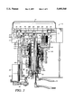
- FIG. 1 is a partial sectional view of the processing chamber of the present invention, showing the receipt of a substrate on the substrate support member thereof.
- FIG. 2 is a sectional view of the processing chamber of the present invention positioned to receive a substrate therein for processing;
- FIG. 3 is an additional sectional view of the processing chamber, positioned for processing a substrate therein;
- FIG. 4 is a top view of the heater plate disposed in the chamber of FIG. 2;
- FIG. 5 is an additional top view of the heater plate of FIG. 5 having a substrate thereon;
- FIG. 6 is a partial, sectional view of the heater plate and substrate edge protection system of FIG. 5 at 6--6.
- the processing chamber 10 of the present invention includes multiple features and embodiments, which may be used independently, or concurrently, to provide improvements in the structure and operation of substrate processing chambers. Referring to FIG. 1, the cooperation and interaction of several of these features are shown, including an internally heated substrate support member, or heater plate 18, a substrate edge protection system 30 in the form of a purge gas channel 220, a substrate alignment member 32 in the form of a plurality of alignment pins 224 on the upper surface of the heater plate 18, and an improved chamber exhaust system 300.
- the heater plate 18 is actuable upwardly within chamber 10 to receive a substrate 24 thereon for processing, and downwardly in chamber 10 to position the substrate 24 therefrom for removal from chamber 10.
- a plurality of support pins 25 are provided to position the substrate 24 on the heater plate 18. These support pins 25 pass through the body of the heater plate 18 and may be extended from the heater plate 18 to receive the substrate 24 as it is placed in the chamber 10 by the robot blade.
- the heater plate 18 may move upwardly with respect to the support pins 25 to position the substrate 24 on the heater plate 18 for processing, and downwardly with respect to the support pins 25 to position the substrate 24 above the heater plate 18 for removal of the substrate 24 from the chamber 10 by the robot blade.
- support pins 25 are shown in FIG. 1 as sinking into heater plate 18. However, it will be appreciated that as the substrate 24 is being received on heater plate 18, support pins 25 and substrate 24 are stationary and heater plate 18 is actually moving upwardly.
- heater plate 18 includes an edge protection system 30, preferably in the form of an integral, circumferential, purge gas channel 220 positioned adjacent the edge 27 of a substrate 24 when the substrate 24 is received on the heater plate 18. Once the substrate 24 is located on heater plate 18 and processing begins, a continuous flow of purge gas is provided to channel 220 about the edge 27 of the substrate 24 to ensure that little, or no, deposition will occur on undesirable portions of the edge 27 of the substrate 24, or on the underside of the substrate 24 immediately adjacent the edge thereof.
- edge protection system 30 preferably in the form of an integral, circumferential, purge gas channel 220 positioned adjacent the edge 27 of a substrate 24 when the substrate 24 is received on the heater plate 18.
- the heater plate 18 includes a substrate alignment member 32, which includes a plurality of tapered guide pins 224 provided above channel 220 along the perimeter thereof to guide the substrate 24 onto the heater plate 18.
- An eccentric and/or misaligned substrate 24 will engage one or more guide pins 224 as the substrate 24 is received onto the heater plate 18.
- the substrate 24 will be forced toward the center of the heater plate 18 at the portion of the substrate 24 edge 27 which touches a guide pin 224. This aligns the entire circumference of the substrate 24 in the proper position with respect to the purge gas channel 220 to ensure passage of purge gas over the entire edge 27 of the substrate 24, except in the very small area where the edge 27 contacts a pin 224.
- the substrate 24 is commonly maintained at an elevated temperature.
- the heater plate 18 of the present invention includes a resistive heating element therein.
- the heater plate 18 heats the substrate 24, which commonly enters the chamber at a temperature lower than that of heater plate 18.
- the substrate edge 27 may load against one or more of the guide pins 224, and if significant thermal expansion occurs thereafter, the substrate edge 27 may chip.
- chamber pressure may be maintained in the plurality of vacuum grooves 77, 78, which are provided in the heater plate upper surface 26 to chuck the substrate 24 to heater plate 18 during processing.
- gas may be introduced therein to reduce the fictional adhesion of the substrate 24 to the heater plate upper surface 26 and thus allow the substrate 24 to expand away from guide pins 224 as the substrate 24 thermally expands.
- the exhaust manifold 23 of the chamber receives a pumping plate 308 thereover, which includes a series of spaced apertures 29 therein.
- the apertures 29 are evenly spaced about the entire circumference of the manifold 23, and the plate 308 spans the gap in the manifold 23 created by the presence of the slit valve 11 in the chamber wall, to increase the uniformity of the removal of reacted gaseous products from the chamber.
- FIGS. 2 and 3 the multiple improvements and features of the chamber 10 of the present invention are shown in a CVD processing apparatus.
- the chamber 10 is shown in partial cutaway to show the interaction and interconnection of the improvements and features of the chamber 10.
- the chamber 10 is shown with the heater plate 18 in the retracted position, wherein a substrate 24 may be positioned on, or removed from, the heads of the support pins 25 which extend from the upper surface of the heater plate 18.
- the apparatus is shown with the heater plate 18 in the extended position with the support pins 25 sunk into the heater plate 18 to position the substrate 24 on the heater plate 18 for processing.
- FIGS. 2 or 3 the discussion of these features may include other Figures necessary to show the details of the features and improvements.
- the CVD processing apparatus of FIGS. 2 and 3 generally includes a chamber 10 having an outer wall 12, a cover 14 and a base 16 which form an evacuatable enclosure 13 in which the vertically-moveable substrate receiving heater plate 18 is located. Heater plate 18 is moveable within enclosure 13 to position a substrate 24 thereon for processing. Heater plate 18 preferably includes the substrate edge protection system 30 as an integral part thereof.
- the heater plate 18 is movable vertically in the enclosure 13 by the stem 20, which is connected to the underside of heater plate 18 and extends outwardly through the base 16 of the enclosure 13 where it is connected to a drive system 22.
- the stem 20 is preferably a right circular, tubular, aluminum member, having an upper end 40 disposed in supporting contact with the underside of the heater plate 18 and a lower end 42 closed off with a cover plate 43.
- the stem lower end 42 is received in a cup shaped sleeve 96, which forms the connection of the stem 20 to the drive system 22.
- cover plate 43 and sleeve 96 include a plurality of aligned apertures therein, through which the heater plate connections are maintained.
- Stem 20 mechanically positions the heater plate 18 within the enclosure 13 and also forms an ambient passageway through which a plurality of heater plate connections extend.
- the heater plate 18 is configured to provide heat to a substrate 24 received on the upper surface 26 thereof, while minimizing the heat transfer therefrom along the stem 20.
- the heater plate 18 is preferably a solid aluminum member, which is welded to the upper end 40 of stem 20.
- the heater plate is heated by a resistive heating element located therein, to provide sufficient heat to maintain the upper surface 26 of the heater plate 18 at elevated processing temperatures of between 250 and 650 degrees celsius.
- the element preferably includes a downwardly projecting tubular portion, which terminates in a blade type connector 64 in the cover plate 43.
- a mating blade connector 62 is located in the sleeve 96, to mate with, and provide electric power to, the connector 64 in the cover plate 43.
- a thermocouple 56 is provided in heater plate 18 to monitor the temperature thereof.
- the heater plate 18 includes a bore 50, extending upwardly therein and terminating adjacent, but interiorly of, the heater plate upper surface 26.
- This bore 50 provides a pilot to receive the end of the thermocouple 56 therein, and also provides an aperture for the receipt of the purge gas and vacuum supplies into the heater plate 18.
- the bore is preferably formed by boring a through hole in the heater plate upper surface 26, and extending a plug 51 and a connector housing 53 into the bore.
- the upper surface of the bore 51 may be slightly recessed from the upper surface 26 of the heater plate 18, or may be ground or otherwise configured to provide a continuous heater plate upper surface 26.
- the connector housing 53 and the plug 51 may be formed as separate elements, or as one continuous element.
- the thermocouple 56 is configured as a rigid rod, which extends through a pair of aligned apertures in the cover plate 43 and the sleeve 96, and terminates within the bore 50 in contact with the solid mass of the heater plate 18 and/or the connector housing 53.
- the lower end of the rigid rod includes a bracket 59, which is releasably attached to the exterior of the sleeve 96, to maintain the thermocouple 56 in position in the heater plate bore 50.
- the bracket is maintained on the exterior of the sleeve 96 by a plurality of screws, but other attachment means, such as clamps or spring clips, may be substituted for the screws.
- thermocouple 56 is connected to an amplifier and a filter for temperature display and over-temperature protection.
- the rigid rod may be slightly smaller in diameter than the aligned apertures in the cover plate 43 and the sleeve 96.
- ambient air will pass through the aligned apertures about the thermocouple 56 and thus be present about thermocouple 56 within the bore 50 in the heater plate 18 to increase the heat transfer between the mass of the heater plate 18 and the thermocouple 56 to increase the accuracy and response time of the thermocouple.
- Purge gas pipe 52 extends through stem 20, from cover plate 43 to the connector housing 53 in the heater plate 18.
- the connector housing 53 includes a plurality of bores therein, which register with purge gas and vacuum bores in the heater plate 18.
- a purge gas bore 70 extends within the heater plate 18, and into a corresponding bore in the connector housing 53, to supply purge gas from the connector housing 53 to the upper surface 26 of the heater plate 18.
- the bore 70 supplies purge gas to a manifold 218 which is ported to a plurality of purge gas apertures 234 extending through the upper surface of heater plate 18 into channel 220 as shown in FIG. 6.
- Vacuum pipe 48 passes through stem 20 from the cover plate 43 on the lower distal end 42 of the stem to upper end 40 of the stem, and is connected through the connector housing 53 in the heater plate 18 to a plurality of vacuum ports 76 extending into a plurality of individual vacuum grooves 77, 78 in the upper surface 26 of heater plate 18.
- a plurality of cross bores 75 are drilled into the heater plate 18 immediately below the upper surface 26, and these cross bores 75 all align into a corresponding bore in the connector housing 53.
- the vacuum pipe 48 terminates into the corresponding bore in the connector housing 53, and thus a vacuum is communicated through the vacuum pipe 48 and into the grooves 77, 78.
- the cover plate 43 and the sleeve 96 include aligned apertures to supply the purge gas and vacuum supplies into the purge gas pipe 52 and vacuum pipe 48 in stem 20, in addition to the apertures therethrough through which the thermocouple 56 and heater element connections extend.
- the purge gas supply, and the vacuum are preferably supplied to the sleeve 96 through bellows tubing, which is connected into fittings threaded into the proper apertures in sleeve 96.
- a circumferential groove is provided about the interface of the aligned apertures through which the vacuum and purge gas supplies are maintained.
- the grooves are preferably located about the exit of the apertures from the upper end of the sleeve 96, and o-ring seals are located in the grooves to seal any gap between the cover plate 43 and the sleeve 96 at the aligned apertures.
- o-rings to seal the gas and vacuum apertures, in conjunction with the use of a blade connector 64 to connect the heating element to the power supply and the use of a rigid rod as the thermocouple, permits relatively simple disassembly of the sleeve 96 from the stem 20.
- the heater plate positioning assembly 34 for positioning the heater plate at multiple locations within the chamber enclosure includes the stem 20 interconnected to the drive system 22.
- Stem 20 is connected to the underside of the heater plate 18, and extends outwardly of the base 16 to connect to the drive system 22.
- the drive system 22 includes a motor and reduction gearing assembly 82 suspended below enclosure 13 and connected with a drive belt 84 to a conformable coupling and lead screw assembly 86.
- a transfer housing 88 is received on lead screw assembly 86, which is guided up and down and held against rotation by a linear slide 90. Transfer housing 88 extends about the circumference of stem 20, and is attached to the lower distal end 42 thereof through the end sleeve 96, to move and support stem 20 and heater plate 18 thereon.
- the motor actuates the lead screw assembly 86 to move stem 20 and heater plate 18 thereon.
- a seal ring 126 is provided in a groove in stem 20 to seal the outer surface of the lower end 42 of stem 20 in sleeve 96.
- Heater plate 18 can droop or sag along its outer edge at the high temperatures used in CVD processing.
- support sleeve 81 is provided to radially support heater plate 18.
- Sleeve 81 includes a lower tubular portion 83, preferably formed of aluminum, received on a ledge 85 on stem 20.
- the ledge 85 may be formed, for example, by locating a snap ring in a groove in the stem 20, which projects radially from stem 20 adjacent stem lower distal end 42 or by machining a circumferential boss on stem 20.
- a spring 87 is received on ledge 85 to receive the base of lower tubular portion 83 thereon to upwardly bias sleeve 81.
- the upper end of sleeve 81 terminates in an outwardly radiating support flange 89, on which a support ring 91, preferably a ceramic ring with high resistance to sagging at elevated temperatures, is received.
- the flange 89 includes an inner circular alignment boss 93 and an outer, upwardly extending lip 95.
- the boss 93 extends into the central aperture in ring 91 to align the ring 91 on the boss 93.
- the support ring 91 is supported on the lip portion 95, to minimize the contact area between the support ring 91 and the sleeve 81.
- a plurality of apertures extend through lip 95, which allow gasses trapped in the interior of the sleeve 81 to vent outwardly therethrough, along the underside of the support ring 91.
- Support ring 91 presses against the lower ring 21 of heater plate 18, and is maintained in contact therewith by the upward bias of spring 87.
- the ceramic does not lose strength at the elevated processing temperature, and thus the ring 91 supports the heater plate 18 against sagging.
- a shroud 94 extends downwardly about stem 20 from the underside of chamber base 16 and terminates on lower end sleeve 96. Shroud 94 and the outer surface of stem 20 extending below aperture 100 form annulus 127 therebetween.
- the annulus 127 communicates with the interior of enclosure 13 through aperture 100, and is thus maintained at the same vacuum pressure as enclosure 13.
- Shroud 94 includes a pair of bellows 98, 99 and a transfer ring 102 which seals the area about the outer circumferential surface of the stem 20 from the atmosphere.
- Each bellows 98, 99 terminates in a support ring 106 a-d.
- Each support ring 106 a-d is a generally right circular member which includes an outwardly projecting support portion 112.
- a seal ring is disposed in projecting support portion 112 to seal the annulus 127 at the support rings 106 a-c.
- annulus 127 is sealed by the interconnection of sleeve 96 and transfer housing 88.
- Seal ring 126 disposed in stem distal end 42, seals the base of stem 20 to sleeve 96 and thus completes the sealing of annulus 127 from the atmosphere.
- the volatile reaction gas When a substrate is processed in chamber 10, the volatile reaction gas will migrate to the bottom of the enclosure 13, and then down through the aperture 100 and into contact with bellows 98, 99, transfer ring 102 and support rings 106 a-d.
- the heat generated by the electric resistance heating element to heat the heater plate 18 for substrate processing conducts through stem 20 to heat bellows 98, 99, support rings 106 a-d, drive system 22 and transfer ring 102.
- the stem 20 is manufactured from one material, preferably an aluminum alloy such as 5086 or 5083 aluminum, and the heater plate 18 is manufactured from a pure aluminum, preferably an 1100 aluminum, or other aluminum material having at least 99% Al and less than 0.05% Mg.
- the 1100 aluminum material may be used in the CVD environment, and need not be anodized.
- the aluminum material of stem 20 preferably has a smaller coefficient of thermal conductivity than the heater plate 18, and thus will transmit heat from heater plate 18 less efficiently than would a stem of a pure aluminum.
- a heat choke portion 44 is provided on stem 20 adjacent heater plate 18, through which a sufficient temperature gradient may be established between heater plate 18 and the lower distal end of stem 20 so that a low-cost flouroelastomer material such as a Viton® material may be used in seal 126.
- water may be provided to coolant passages provided within sleeve 96.
- a water jacket may be placed around the sleeve 96, or transfer case 88 and transfer ring 102, to help cool these components during and after substrate 24 processing.
- a cooling fan may be used to pass air over the components to increase heat transfer therefrom.
- sleeve 96 also includes a purge gas manifold 97 formed at the interface of the sleeve 96 and the lower support ring 106d, into which a supply of purge gas, such as Argon, may be provided.
- the purge gas flows outwardly from the manifold 97, from a plurality of holes spaced about the manifold 97, preferably 8 to 12 holes, and then upwardly through annulus 127, to maintain a gas barrier against entry of reactive gasses through aperture 100 into annulus 127.
- the flow of purge gas through the manifold 97 is preferably maintained at a flow rate which will maintain laminar plug flow of purge gas upwardly in the annulus 127. By maintaining these conditions, the diffusion of the reactive gas downwardly through the aperture 100 will be substantially eliminated. Additionally, during processing, the purge gas passes up through aperture 100 and about the outer edge of the heater plate 18 to minimize the passage of reactive gas down about the sides of heater plate 18. This reduces the amount of reactive gas which reaches the interior surfaces of the structural components of the chamber, and the underside of the heater plate 18, to reduce the amount of unwanted material deposition which may occur on these surfaces.
- Stem 20 moves upwardly and downwardly through the aperture 100 in base 16 of enclosure 13, to move heater plate 18 to receive a substrate 24 thereon and, after processing, to move heater plate 18 into a position where the substrate 24 may be removed from the enclosure 13 by a robot blade.
- the substrate positioning assembly 140 includes a plurality of support pins 25 which move with respect to heater plate 18 to support the substrate 24 in position to be placed in, or removed from, the enclosure 13, and to locate the substrate 24 on the heater plate 18.
- the support pins 25 are received in sleeves in bores 130 disposed vertically through heater plate 18.
- Each pin 25 includes a cylindrical shaft 132 terminating in a lower spherical portion 134 and an upper truncated conical head 136 formed as an outward extension of shaft 132.
- Bore 130 includes an upper, countersunk portion 138 sized to receive enlarged head 136 therein such that when pin 25 is fully received into heater plate 18, head 136 does not extend above the surface of heater plate 18.
- support pins 25 move partially in conjunction with, and partially independently of, heater plate 18 as heater plate 18 moves within enclosure 13.
- Support pins 25 must extend from heater plate 18 to allow the robot blade to remove the substrate 24 from the enclosure 13, but must also sink into heater plate 18 to locate the substrate 24 on the upper surface 26 of heater plate 18 for processing.
- a substrate positioning assembly 140 is provided which is normally biased upwardly into enclosure 13, but is also moveable downwardly by the stem 20 as stem 20 moves to actuate heater plate 18 downwardly in enclosure 13.
- Substrate positioning assembly 140 includes an annular pin support 142 which is configured to engage lower spherical portions 134 of support pins 25, and a drive member 144 which positions pin support 142 to selectively engage support pins 25 depending upon the position of heater plate 18 within chamber.
- Pin support 142 includes an upper pin support ring 146, preferably made from ceramic, which extends around the underside of heater plate 18 to selectively engage the lower spherical portions 134 of support pins 25, and a sleeve portion 150 which extends downwardly from pin support ring 146 through aperture 100 to terminate on transfer ring 102.
- Transfer ring 102 is disposed circumferentially about stem 20, and is keyed to slide 90 to prevent rotation thereof.
- the sleeve portion 150 includes a lower cylindrical portion 149, and an outwardly extending radial support 151 which receives and supports pin support 146 thereon.
- the radial support 151 includes an upper, generally flat, upper surface having a circumferential alignment wall 153 which aligns with the inner diameter of the annular pin support 146 and a plurality of upwardly supporting support ribs 155 which support the underside of the pin support ring 146.
- gases may become trapped along the interior of cylindrical portion 149, which could damage the chamber components.
- a plurality of gaps 157 are formed adjacent the support ribs 155, and a plurality of holes 159 are formed through lower cylindrical potion 149. The holes 159 and gaps 157 allow the free flow of gases from the interior to the exterior of the sleeve 150.
- Pin drive member 144 is located on the underside of enclosure 13 to control the movement of sleeve portion 150 with respect to heater plate 18, and includes therefore a spring assembly 156 which is connected to transfer ring 102 to provide the upward bias on transfer ring 102 and sleeve portion 150 to bias pin support ring 146 upwardly to push the support pins 25 upwardly through the heater plate 18, and the snap ring or ledge 84 on stem 20 which is selectively engageable with sleeve 150 to move sleeve portion 150 and pin support ring 146 attached thereto downwardly after heater plate 18 has moved a preselected distance downwardly in enclosure 13.
- Spring assembly 156 includes a housing 158 having a slot 160 therethrough, which is attached to the underside of enclosure 13 adjacent aperture 100.
- a spring-loaded finger 154 extends through slot 160, and is upwardly biased by a spring 164 in housing 158.
- Finger 154 is rigidly connected to transfer ring 102, and thus upwardly biases sleeve 150 attached thereto.
- the upper terminus of housing 158 limits the upward movement of finger 154.
- Transfer ring 102 is also rigidly connected to support ring 106c, which includes a downwardly extending tubular portion which terminates in an inwardly extending flange 173.
- the ledge 85 which supports sleeve 81 on stem 20, is also engageable against flange 173 as stem 20 moves downwardly.
- support pins 25 remain stationary and support the substrate 24 in a stationary position within chamber as heater plate 18 continues moving downwardly.
- the ledge 85 on stem 20 engages flange 173, which locks stem 20 to sleeve 150 and causes heater plate 18 and pin support ring 146 to move downwardly in unison.
- the support pins 25 remain stationary with respect to heater plate 18, and both elements move downwardly in enclosure 13.
- Stem 20 then moves to move sleeve 150 and heater plate 18 upwardly.
- finger 154 engages the top of housing 158 sleeve 150 becomes stationary, while ledge 85 moves off flange 173 as stem 20 continues moving upwardly, and thus continued movement of heater plate 18 sinks support pins 25 therein to position the substrate 24 thereon for processing.
- the overall length of the support pins 25 may be minimized, and the length of the pin shaft 132 which is exposed below the heater plate 18 and support ring 91 during processing is equal to the distance from the heater plate 18 that the substrate 24 is located when the substrate 24 is being manipulated on and off the support pins 25 by the robot blade.
- minimal support pin 25 surface area is exposed during processing, and therefore minimal deposits will occur on the support pins 25.
- the upper surface 26 of heater plate 18 includes a plurality of concentric grooves 78 therein, which intersect with a plurality of radial grooves 77.
- a plurality of vacuum ports 76 are disposed to communicate between the base of each radial groove 77 and the circular vacuum manifold 75 disposed within heater plate 18.
- Vacuum pipe 48 communicates with manifold 75 to supply the vacuum thereto.
- Vacuum ports 76 and grooves 77, 78 provide a low pressure environment under the substrate 24 to chuck the substrate 24 to the heater plate upper portion 26.
- enclosure 13 may be maintained at about 80 torr.
- a vacuum of 1.5 torr to 60 torr is drawn through vacuum pipe 48, and thus through ports 76 to grooves 77, 78.
- the 20 to 78 torr pressure differential between grooves 77, 78 and enclosure 13 causes the substrate 24 to adhere to the heater plate top surface 26 to increase the heat transfer from the heater plate 18 to the substrate 24.
- grooves 77, 78 may maintain a lower pressure than that present in enclosure 13, which may firmly adhere the substrate 24 to heater plate upper surface 26.
- support pins 25 can crack the substrate as it is forced off the heater plate 18.
- a bypass line may be provided between the vacuum pipe 48 inlet and the chamber slit valve 11. When the heater plate is actuated to remove the substrate 24 from the chamber 10, the bypass line is opened to communicate between the grooves 77, 78 and the enclosure 13.
- Heater plate top surface 26 may also include a groove, or plurality of grooves, located adjacent the outer circumference thereof which are not connected to the vacuum. These grooves reduce the area of contact between the substrate 24 and heater plate 18, which reduces the heat transfer to, and thus deposited film thickness on, the substrate edge 27.
- substrates 24 may become sufficiently misaligned, with respect to the chamber components, that the substrate 24 may be tipped with respect to heater plate upper surface 26. Additionally, substrates 24 may be cracked or warped. In each instance, the continued processing of the substrate 24 can allow the processing gas to contact the internal areas of the heater plate 18 which can effect the integrity of the heater plate 18, can create particles, or can free portions of the cracked substrates into the chamber. In these instances, it is desirable to immediately stop the processing to remove the substrate 24 before chamber damage occurs.
- a pressure sensor 49 is located in the vacuum line at the inlet to the vacuum pump to transmit a signal to a shut down controller, which shuts down chamber operation when the vacuum pressure is indicative of a cracked, warped or misaligned substrate.
- the substrate edge protection system 30 When a substrate is located on the upper surface 26 of heater plate 18, the substrate edge protection system 30 provides and a gas which passes about the perimeter of the substrate 24 to prevent material deposits on that area of the substrate 24.
- Substrate 24 has a circumferential edge 27 extending around the periphery thereof, which includes an upper tapered surface 17, a lower tapered surface 19 and a generally flat middle circumferential portion 21.
- the deposition layer should be evenly deposited all the way to the edge 27 of the substrate, but not occur on the underside, lower tapered surface 19 or flat middle portion 21 of the substrate 24 where it may contact other materials and become dislodged.
- the substrate edge protection system 30 of the present invention addresses this requirement.
- the upper surface 26 of heater plate 18 is configured to provide an integral purge gas channel 220 to supply a relatively constant supply of purge gas about the entire perimeter of substrate 24.
- heater plate upper surface 26 terminates in an upwardly projecting guide receiving portion 222 which is an annular flat raised portion, disposed 0.002 to 0.005 inches above upper surface 26.
- Purge gas channel 220 is formed as an inwardly extending groove, disposed at an approximately 135° angle from upper surface 26, at the interface of upper surface 26 and the base of the inner edge of guide receiving portion 222.
- a plurality of purge gas holes 234 are disposed between the inner terminus of purge gas channel 220 and the purge gas manifold 218, and are evenly spaced circumferentially about the heater plate 18 to supply the purge gas from manifold 218 into channel 220.
- the number of holes 234 is dependant upon the intended distance between the substrate edge 27 and the bottom of the channel 220. With a distance from the point of entry of the hole 234 into the channel 220 to the substrate edge 27 of 0.060 inches, the number of holes is approximately two - hundred and forty. As the distance from the hole 234 opening to the wafer edge 27 increases, the number of holes necessary to provide a constant flow of purge gas at substrate edge 27 decreases. Where the distance from the opening of hole 234 to the substrate edge 27 is doubled, the number of holes 234 is approximately halved.
- the preferred substrate alignment member 32 includes a plurality of ceramic guide pins 224 disposed on guide receiving portion 222 adjacent channel 220.
- Each pin 224 includes a front portion 226 tapered approximately 12 degrees from vertical.
- Front portion 226 includes a generally flat extending central portion 230, and tapered sides 228, such that central portion 230 extends further inward toward the center of the heater plate upper surface 26 than tapered sides 228.
- Central portion 230 extends inwardly from guide receiving portion 222 and over purge gas channel 220.
- Each pin 224 also includes a rearwardly extending mounting tab 231 , which includes a pair of holes therein for receipt of bolts to secure the pin 224 to guide receiving portion 222.
- the guide pins 224 are located on heater plate 18 such that extending central portions 230 of the pins 224 are disposed approximately five to seven thousandths of an inch from substrate flat middle circumferential portion 21 when substrate 24 is perfectly aligned to the center of heater plate 18. Thus, in the instance where the substrate 24 is perfectly aligned, the substrate 24 will come into contact with upper surface 26 without touching any of pins 224. However, most substrates have a slight amount of eccentricity, and the robot blade does not always perfectly center the substrate 24 on upper surface 26.
- lower tapered surface 19 and flat middle circumferential portion 21 of substrate 24 will engage one, or more, extending portions 230 of guide pins 224, and the guide pins 224 will align the substrate into position on upper surface 26 so that edge 27 does not substantially block purge gas channel 220.
- the guide pins 224 By positioning the substrate 24 with guide pins 224, the only portion of the substrate 24 which touches the alignment mechanism is that small portion of edge 27 in contact with guide pin central portion 230.
- central portion 230 extends radially inwardly from purge gas channel 220, substrate edge 27 will locate a small distance from the channel 220, and the area of substrate 24 to each side of the contact area of substrate 24 with central portion 230 will receive an uninterrupted supply of purge gas.
- the present invention specifically contemplates the use of reactive gasses, in addition to the purge gas, as the masking gas.
- a reactive species such as H 2
- deposition at the substrate edge may be selectively enhanced if desired.
- the temperature thereof may be substantially lower than the heater plate 18 temperature. Once the substrate 24 comes into contact with the heater plate 18, heat is transferred into the substrate 24 to raise its temperature to the processing temperature. This temperature increase causes thermal expansion of the substrate 24, such that edge 27 thereof may press against alignment pins 224. Further, the vacuum in grooves 77, 78 firmly adheres the substrate 24 to heater plate 18 upper surface 26, such that the edge 27 of substrate 24 may become compressively loaded against pin 224. As a result of this loading, the substrate 24 can crack or chip where it touches alignment pin 224.
- the chamber controller may be programmed to maintain the chamber pressure in the vacuum grooves 77, 78 during the period when the substrate 24 is heated, and then pull a vacuum through the grooves 77, 78 after the substrate 24 reaches a stable temperature.
- the presence of chamber pressure below substrate 24 allows the substrate to expand away from the area of contact with alignment pin 224, thus reducing localized compressive stresses and reducing the incidence of compressive cracking or chipping on the substrate edge 27.
- purge gas may be backflushed through vacuum grooves 77, 78 as the substrate 24 is received on upper surface 26 to help align the substrate 24 and reduce frictional adhesion of the substrate 24 to support pins 25 as guide pins 224 guide the substrate 24 into position, or gas may be backflushed through the grooves 77, 78 as the substrate 24 thermally expands to allow the substrate 24 to expand away from pins 224 when received on heater plate upper surface 26.
- the top 12 of chamber 10 includes a prior art manifold 23 which leads to the exhaust port 304 of the chamber 10. Suction through the exhaust port 304 pulls exhausted chamber gasses out of enclosure 13 to maintain the proper processing environment in enclosure 13.
- Manifold 23 extends substantially around the perimeter of top 14, but a gap remains where wall 16 is pierced by the slit valve 11. This gap creates uneven exhausting and thus uneven chamber processing gas distribution throughout the enclosure 11.
- a pumping plate 308 with a plurality of apertures 29 evenly spaced thereabout, is mounted over manifold 23.
- Apertures 29 are spaced apart approximately 30 degrees, and an aperture 29 is spaced at each end of manifold 23 adjacent the gap.
- the evenly spaced apertures in pumping plate 308 create even exhausting of used chamber processing materials, which leads to the creation of a more uniform deposition layer on the substrate 24.
- the foregoing embodiments of the invention provide a CVD chamber which yields a more uniform deposition material layer on the substrate, while simultaneously reducing the incidence of particle generation during processing.
- the overall yield of die from the substrates is increased by reducing localized temperature variation at the substrate edge and eliminating the masked edge of the substrate created by the shadow ring.
- the uniformity of the deposition is enhanced, by creating a uniform exhausting of reacted products from the enclosure 13.
- the structure of the improved CVD chamber also leads to reduced particle generation. Rubbing of the substrate 24 on heater plate 18 upper surface 26 is reduced, by reducing the frictional adhesion of the substrate 24 and heater plate 18 as the substrate is received thereon, by eliminating contact between the shadow ring and substrate 24, and by reducing the amount of deposition material received on the chamber components.
Abstract
An improved deposition chamber deposits useful layers on substrates. The improved chamber includes a substrate edge protection system which, in combination with a purge gas, protects selected portions of the edge and underside of the substrate from the deposition gas while preventing the creation of a masked area on the substrate edge. The substrate is supported on a solid receiving plate, which is supported by a stem having a heat limiting member and a shroud to protect the stem and a positioning assembly aligns the substrate to the receiving plate.
Description
This is a continuation-in-part of U.S. patent application Ser. No. 08/042,961 filed Apr. 5, 1993.
The present invention relates to methods and apparatus for depositing useful layers of materials on substrates used in the manufacture of semiconductor die. More particularly, the invention relates to improved apparatus and methods for use in the processing of substrates, such as by chemical vapor deposition.
Chemical vapor deposition, commonly referred to as "CVD," is used to deposit a thin layer of material on a semiconductor substrate. To process substrates with the CVD process, a vacuum chamber is provided with a susceptor configured to receive a substrate thereon. In a typical prior art CVD chamber, the substrate is placed into and removed from the chamber by a robot blade. The chamber includes an intermediate substrate positioning assembly on which the substrate is located when it is placed into, or about to be removed from, the chamber. To locate the substrate on the susceptor, the susceptor is passed through the center of the substrate positioning assembly to lift the substrate therefrom. The susceptor and the substrate are then heated to a temperature of between 250°-650° C. Once the substrate is located on the susceptor and heated to an appropriate temperature, a precursor gas is charged to the vacuum chamber through a gas manifold situated above the substrate. The precursor gas reacts with the heated substrate surface to deposit the thin material layer thereon. As the gas reacts to form the material layer, volatile byproduct gasses are formed, and these gasses are pumped out of the vacuum chamber through a chamber exhaust system.
A primary goal of substrate processing is to obtain as many useful die as possible from each substrate. Many factors influence the processing of substrates in the CVD chamber and affect the ultimate yield of die from each substrate processed therein. These factors include processing variables, which affect the uniformity and thickness of the deposition material layer deposited on the substrate, and contaminants that can attach to the substrate and contaminate one or more die therein. Both of these factors must be controlled in CVD and other processes to maximize the die yield from each substrate.
One CVD processing variable which affects the uniformity of the deposition material layer is the relative concentration of reacted and non-reacted process gas components in the deposition chamber. The exhaust system of the chamber includes a circumferential exhaust channel located above the substrate adjacent the perimeter thereof, through which the reacted process gas is vented. However, a gap exists in the circumferential exhaust channel where the slit valve for moving the substrate into and out of the chamber passes through the chamber wall. The exhausting of reacted gaseous products from the chamber is less efficient near this gap, and thus the exhausting of reaction products is non-uniform in the chamber. This contributes to the creation of non-uniform deposition material layers on the substrate, because the relative concentration of reactive gas in the total gas volume in the chamber varies about the surface of the substrate due to the non-uniform exhausting of reacted gaseous products from the chamber.
In addition to the foregoing factor which affects the uniformity and thickness of the deposition material layer, CVD processing chambers include multiple sources of particle contaminants which, if received on the substrate, reduce the die yield therefrom. One primary source of particulate contamination in CVD processing is the deposition material deposited on the chamber surfaces during processing. As the substrate is processed in the CVD chamber, a material layer is indiscriminately deposited on all surfaces within the chamber which are contacted with the gas, such as lamp covers. If these chamber surfaces are later touched or rubbed, or if the material layer is loosely attached to the chamber surface and the chamber is shaken or vibrated, particles of deposition material layer can become free in the chamber and contaminate the substrate. Additionally, the deposition material layer does not typically firmly attach itself to the edge and underside of the substrate, and the layer formed in that location of the substrate is known to flake off the substrate and become a particle contaminant.
One method of controlling particle generation in the chamber is to use a shadow ring to reduce the occurrence of the deposition layer on the edge and underside of the substrate. A shadow ring is a masking member, which is received on the susceptor and contacts the upper, outer, circumferential area of the substrate and limits access of the deposition gas to the contacted area of the substrate. However, the shadow ring has several limitations which contribute to the non-uniform processing of substrates. The volatile deposition gas still tends to migrate under the lip of the shadow ring and deposit a material layer on the substrate edge and underside which may later flake off. Additionally, the engagement of the shadow ring with the substrate can create particles. Finally, the shadow ring is a heat sink, which draws heat out of the substrate and thus reduces the temperature of the substrate adjacent the area of contact between the substrate and shadow ring, which affects the thickness of the deposition material layer on the area of the substrate adjacent the shadow ring.
One alternative to the shadow ring is disclosed in European Patent Application No. EPO 467 623 A3, published Jan. 22, 1992. In that application, a shroud is provided around the perimeter of the substrate. The shroud includes a lip which overhangs, but does not touch, the substrate. A gas is provided to the underside of the substrate, and a portion of this gas flows outwardly between the substrate and susceptor and into a gap formed between the substrate and the shroud. Although the shroud creates a circumferential channel in which a non-reactive gas may be maintained to mask the edge of the substrate, the structure shown in EPO 467 623 A3 has several disadvantages. First, when the shroud is received on the susceptor, it aligns with the susceptor and no means is disclosed for aligning the substrate with the shroud. Any substantial misalignment between the substrate and the susceptor will result in substantial misalignment between the shroud and substrate, and the resulting annular gap between the substrate and shroud will be non-uniform around the perimeter of the substrate. This will create differential masking gas flow in different locations of the substrate edge. Second, introduction of the masking gas inwardly of the outer diameter of the substrate can cause the substrate to float off the susceptor during processing if the chamber pressure and process gas flow are not closely controlled. Finally, the European application notes that the shroud disclosed therein masks the upper surface of the substrate and prevents depositions thereon, which reduces the useful area of the substrate.
A further source of substrate particulate contamination occurs where a cracked, warped or substantially misaligned substrate is present in the chamber. If a cracked, warped or substantially misaligned substrate is encountered, substantial numbers of particulate contaminants can be generated as the substrate is moved in the chamber. Additionally, if large segments of the substrate become free in the chamber, they may seriously damage the chamber components. Finally, the upper surface and passageways of the susceptor could be exposed to the corrosive reactive gas if a cracked, warped or misaligned substrate is processed in the chamber.
The present invention is useful as a CVD processing apparatus for depositing blanket and selectively deposited tungsten, tungsten silicide, titanium nitride and other deposition materials with improved uniformity and controllability. The invention includes multiple embodiments which may be used independently or concurrently to improve the control of processing variables and/or reduce the incidence of contamination of the substrate during processing. Although the embodiments of the invention are discussed with reference to a CVD chamber, the embodiments of the invention are applicable to other substrate processes and process environments.
In a first embodiment of the invention, the apparatus includes a chamber having a substrate support member on which the substrate is located for processing. The substrate is positioned on the substrate support member with a positioning means, which positions the substrate above the support member for insertion and removal of the substrate through the chamber slit valve, and also positions the substrate on the surface of the support member for processing. The positioning means positions the substrate partially in conjunction with, and partially independently of, movement of the support member.
In a second embodiment of the invention, the substrate edge protection system of the chamber includes a manifold extending circumferentially about the edge of the substrate when the substrate is received on the support member. The manifold distributes a gas around the edge of the substrate. An alignment member may also be provided, to align the substrate edge with the channel. As the substrate does not touch the underside of a shadow ring, particle generation is reduced, the uniformity of the deposition material layer is increased, and the useable area of the substrate is increased.
To secure the substrate to the receiving plate during processing, depressions may be provided in the upper surface of the plate and ported to a vacuum source. In a further embodiment of the invention, a pressure sensor is disposed in the vacuum line which supplies the vacuum to the depressions, which monitors pressure changes in the vacuum line corresponding to the presence of a cracked, warped or substantially misaligned substrate on the support member. In an additional embodiment of the invention, a purge gas is circulated through the underside of the chamber, to protect the mechanical componentry of the chamber from corrosive attack and reduce the formation of deposits on the interior chamber surfaces. In a still further embodiment of the invention, the chamber includes an extended pumping plate which extends around the circumference of the chamber about the edge of the substrate and spans the gap in the exhaust channel to uniformly pump reacted volatile gas from the chamber.
These, and other features and advantages of the invention will be apparent from the following description when read in conjunction with the accompanying drawings, wherein:
FIG. 1 is a partial sectional view of the processing chamber of the present invention, showing the receipt of a substrate on the substrate support member thereof.
FIG. 2 is a sectional view of the processing chamber of the present invention positioned to receive a substrate therein for processing;
FIG. 3 is an additional sectional view of the processing chamber, positioned for processing a substrate therein;
FIG. 4 is a top view of the heater plate disposed in the chamber of FIG. 2;
FIG. 5 is an additional top view of the heater plate of FIG. 5 having a substrate thereon; and
FIG. 6 is a partial, sectional view of the heater plate and substrate edge protection system of FIG. 5 at 6--6.
The processing chamber 10 of the present invention includes multiple features and embodiments, which may be used independently, or concurrently, to provide improvements in the structure and operation of substrate processing chambers. Referring to FIG. 1, the cooperation and interaction of several of these features are shown, including an internally heated substrate support member, or heater plate 18, a substrate edge protection system 30 in the form of a purge gas channel 220, a substrate alignment member 32 in the form of a plurality of alignment pins 224 on the upper surface of the heater plate 18, and an improved chamber exhaust system 300.
The heater plate 18 is actuable upwardly within chamber 10 to receive a substrate 24 thereon for processing, and downwardly in chamber 10 to position the substrate 24 therefrom for removal from chamber 10. To position the substrate 24 on the heater plate 18, a plurality of support pins 25 are provided. These support pins 25 pass through the body of the heater plate 18 and may be extended from the heater plate 18 to receive the substrate 24 as it is placed in the chamber 10 by the robot blade. The heater plate 18 may move upwardly with respect to the support pins 25 to position the substrate 24 on the heater plate 18 for processing, and downwardly with respect to the support pins 25 to position the substrate 24 above the heater plate 18 for removal of the substrate 24 from the chamber 10 by the robot blade. For ease of illustration, support pins 25 are shown in FIG. 1 as sinking into heater plate 18. However, it will be appreciated that as the substrate 24 is being received on heater plate 18, support pins 25 and substrate 24 are stationary and heater plate 18 is actually moving upwardly.
To reduce the occurrence of the deposition layer on the substrate underside and edge, heater plate 18 includes an edge protection system 30, preferably in the form of an integral, circumferential, purge gas channel 220 positioned adjacent the edge 27 of a substrate 24 when the substrate 24 is received on the heater plate 18. Once the substrate 24 is located on heater plate 18 and processing begins, a continuous flow of purge gas is provided to channel 220 about the edge 27 of the substrate 24 to ensure that little, or no, deposition will occur on undesirable portions of the edge 27 of the substrate 24, or on the underside of the substrate 24 immediately adjacent the edge thereof. To fully exploit the purge gas channel 220, the positioning of the substrate 24 on the heater plate 18 is critical, as any gross misalignment will place a portion of the substrate 24 edge in a position which substantially blocks the channel 220. Therefore, the heater plate 18 includes a substrate alignment member 32, which includes a plurality of tapered guide pins 224 provided above channel 220 along the perimeter thereof to guide the substrate 24 onto the heater plate 18. An eccentric and/or misaligned substrate 24 will engage one or more guide pins 224 as the substrate 24 is received onto the heater plate 18. As the heater plate 18 approaches the substrate 24 supported over the heater plate 18 on support pins 25, the substrate 24 will be forced toward the center of the heater plate 18 at the portion of the substrate 24 edge 27 which touches a guide pin 224. This aligns the entire circumference of the substrate 24 in the proper position with respect to the purge gas channel 220 to ensure passage of purge gas over the entire edge 27 of the substrate 24, except in the very small area where the edge 27 contacts a pin 224.
During processing, the substrate 24 is commonly maintained at an elevated temperature. To establish and maintain this temperature, the heater plate 18 of the present invention includes a resistive heating element therein. The heater plate 18 heats the substrate 24, which commonly enters the chamber at a temperature lower than that of heater plate 18. As the substrate is heated to the processing temperature, the substrate edge 27 may load against one or more of the guide pins 224, and if significant thermal expansion occurs thereafter, the substrate edge 27 may chip. To address this problem, chamber pressure may be maintained in the plurality of vacuum grooves 77, 78, which are provided in the heater plate upper surface 26 to chuck the substrate 24 to heater plate 18 during processing. Alternatively, gas may be introduced therein to reduce the fictional adhesion of the substrate 24 to the heater plate upper surface 26 and thus allow the substrate 24 to expand away from guide pins 224 as the substrate 24 thermally expands.
To increase the uniformity of the exhaust of reacted gaseous products within the chamber 10, the exhaust manifold 23 of the chamber receives a pumping plate 308 thereover, which includes a series of spaced apertures 29 therein. The apertures 29 are evenly spaced about the entire circumference of the manifold 23, and the plate 308 spans the gap in the manifold 23 created by the presence of the slit valve 11 in the chamber wall, to increase the uniformity of the removal of reacted gaseous products from the chamber.
These features, and other additional features of the invention described herein, may be used independently or concurrently to provide improvements in the processing of substrates in the chamber.
Referring now to FIGS. 2 and 3, the multiple improvements and features of the chamber 10 of the present invention are shown in a CVD processing apparatus. In FIGS. 2 and 3, the chamber 10 is shown in partial cutaway to show the interaction and interconnection of the improvements and features of the chamber 10. In FIG. 2, the chamber 10 is shown with the heater plate 18 in the retracted position, wherein a substrate 24 may be positioned on, or removed from, the heads of the support pins 25 which extend from the upper surface of the heater plate 18. In FIG. 3, the apparatus is shown with the heater plate 18 in the extended position with the support pins 25 sunk into the heater plate 18 to position the substrate 24 on the heater plate 18 for processing. Although the features and improvements of the chamber 10 are shown in FIGS. 2 or 3, the discussion of these features may include other Figures necessary to show the details of the features and improvements.
The CVD processing apparatus of FIGS. 2 and 3 generally includes a chamber 10 having an outer wall 12, a cover 14 and a base 16 which form an evacuatable enclosure 13 in which the vertically-moveable substrate receiving heater plate 18 is located. Heater plate 18 is moveable within enclosure 13 to position a substrate 24 thereon for processing. Heater plate 18 preferably includes the substrate edge protection system 30 as an integral part thereof.
The heater plate 18 is movable vertically in the enclosure 13 by the stem 20, which is connected to the underside of heater plate 18 and extends outwardly through the base 16 of the enclosure 13 where it is connected to a drive system 22. The stem 20 is preferably a right circular, tubular, aluminum member, having an upper end 40 disposed in supporting contact with the underside of the heater plate 18 and a lower end 42 closed off with a cover plate 43. The stem lower end 42 is received in a cup shaped sleeve 96, which forms the connection of the stem 20 to the drive system 22. To provide connections from the exterior of the chamber into the heater plate 18, cover plate 43 and sleeve 96 include a plurality of aligned apertures therein, through which the heater plate connections are maintained. Stem 20 mechanically positions the heater plate 18 within the enclosure 13 and also forms an ambient passageway through which a plurality of heater plate connections extend.
The heater plate 18 is configured to provide heat to a substrate 24 received on the upper surface 26 thereof, while minimizing the heat transfer therefrom along the stem 20. The heater plate 18 is preferably a solid aluminum member, which is welded to the upper end 40 of stem 20. Preferably, the heater plate is heated by a resistive heating element located therein, to provide sufficient heat to maintain the upper surface 26 of the heater plate 18 at elevated processing temperatures of between 250 and 650 degrees celsius. To power the heating element, the element preferably includes a downwardly projecting tubular portion, which terminates in a blade type connector 64 in the cover plate 43. A mating blade connector 62 is located in the sleeve 96, to mate with, and provide electric power to, the connector 64 in the cover plate 43.
Referring to FIG. 2, a thermocouple 56 is provided in heater plate 18 to monitor the temperature thereof. The heater plate 18 includes a bore 50, extending upwardly therein and terminating adjacent, but interiorly of, the heater plate upper surface 26. This bore 50 provides a pilot to receive the end of the thermocouple 56 therein, and also provides an aperture for the receipt of the purge gas and vacuum supplies into the heater plate 18. The bore is preferably formed by boring a through hole in the heater plate upper surface 26, and extending a plug 51 and a connector housing 53 into the bore. The upper surface of the bore 51 may be slightly recessed from the upper surface 26 of the heater plate 18, or may be ground or otherwise configured to provide a continuous heater plate upper surface 26. The connector housing 53 and the plug 51 may be formed as separate elements, or as one continuous element. The thermocouple 56 is configured as a rigid rod, which extends through a pair of aligned apertures in the cover plate 43 and the sleeve 96, and terminates within the bore 50 in contact with the solid mass of the heater plate 18 and/or the connector housing 53. The lower end of the rigid rod includes a bracket 59, which is releasably attached to the exterior of the sleeve 96, to maintain the thermocouple 56 in position in the heater plate bore 50. Preferably, the bracket is maintained on the exterior of the sleeve 96 by a plurality of screws, but other attachment means, such as clamps or spring clips, may be substituted for the screws. The thermocouple 56 is connected to an amplifier and a filter for temperature display and over-temperature protection. To ensure that air is present in the bore 50, the rigid rod may be slightly smaller in diameter than the aligned apertures in the cover plate 43 and the sleeve 96. Thus, ambient air will pass through the aligned apertures about the thermocouple 56 and thus be present about thermocouple 56 within the bore 50 in the heater plate 18 to increase the heat transfer between the mass of the heater plate 18 and the thermocouple 56 to increase the accuracy and response time of the thermocouple.
Referring now to FIG. 3, the purge gas supply for supplying a protective gas to the substrate edge protection system 30 is shown. Purge gas pipe 52 extends through stem 20, from cover plate 43 to the connector housing 53 in the heater plate 18. The connector housing 53 includes a plurality of bores therein, which register with purge gas and vacuum bores in the heater plate 18. A purge gas bore 70 extends within the heater plate 18, and into a corresponding bore in the connector housing 53, to supply purge gas from the connector housing 53 to the upper surface 26 of the heater plate 18. In the preferred substrate edge protection system, the bore 70 supplies purge gas to a manifold 218 which is ported to a plurality of purge gas apertures 234 extending through the upper surface of heater plate 18 into channel 220 as shown in FIG. 6.
Referring now to FIGS. 3 and 4, the vacuum supply to heater pipe 18 is shown. Vacuum pipe 48 passes through stem 20 from the cover plate 43 on the lower distal end 42 of the stem to upper end 40 of the stem, and is connected through the connector housing 53 in the heater plate 18 to a plurality of vacuum ports 76 extending into a plurality of individual vacuum grooves 77, 78 in the upper surface 26 of heater plate 18. To supply the vacuum ports 76, a plurality of cross bores 75 are drilled into the heater plate 18 immediately below the upper surface 26, and these cross bores 75 all align into a corresponding bore in the connector housing 53. The vacuum pipe 48 terminates into the corresponding bore in the connector housing 53, and thus a vacuum is communicated through the vacuum pipe 48 and into the grooves 77, 78.
The cover plate 43 and the sleeve 96 include aligned apertures to supply the purge gas and vacuum supplies into the purge gas pipe 52 and vacuum pipe 48 in stem 20, in addition to the apertures therethrough through which the thermocouple 56 and heater element connections extend. The purge gas supply, and the vacuum, are preferably supplied to the sleeve 96 through bellows tubing, which is connected into fittings threaded into the proper apertures in sleeve 96. To prevent leakage of the vacuum or purge gas at the interface of the cover plate 43 and the sleeve 96, a circumferential groove is provided about the interface of the aligned apertures through which the vacuum and purge gas supplies are maintained. The grooves are preferably located about the exit of the apertures from the upper end of the sleeve 96, and o-ring seals are located in the grooves to seal any gap between the cover plate 43 and the sleeve 96 at the aligned apertures. The use of o-rings to seal the gas and vacuum apertures, in conjunction with the use of a blade connector 64 to connect the heating element to the power supply and the use of a rigid rod as the thermocouple, permits relatively simple disassembly of the sleeve 96 from the stem 20.
The heater plate positioning assembly 34 for positioning the heater plate at multiple locations within the chamber enclosure includes the stem 20 interconnected to the drive system 22. Stem 20 is connected to the underside of the heater plate 18, and extends outwardly of the base 16 to connect to the drive system 22. The drive system 22 includes a motor and reduction gearing assembly 82 suspended below enclosure 13 and connected with a drive belt 84 to a conformable coupling and lead screw assembly 86. A transfer housing 88 is received on lead screw assembly 86, which is guided up and down and held against rotation by a linear slide 90. Transfer housing 88 extends about the circumference of stem 20, and is attached to the lower distal end 42 thereof through the end sleeve 96, to move and support stem 20 and heater plate 18 thereon. The motor actuates the lead screw assembly 86 to move stem 20 and heater plate 18 thereon. A seal ring 126 is provided in a groove in stem 20 to seal the outer surface of the lower end 42 of stem 20 in sleeve 96.
When a substrate is processed in chamber 10, the volatile reaction gas will migrate to the bottom of the enclosure 13, and then down through the aperture 100 and into contact with bellows 98, 99, transfer ring 102 and support rings 106 a-d. The heat generated by the electric resistance heating element to heat the heater plate 18 for substrate processing conducts through stem 20 to heat bellows 98, 99, support rings 106 a-d, drive system 22 and transfer ring 102. The heat radiated and conducted by the stem 20, in conjunction with the presence of the reactive gas, creates a corrosive environment for support rings 106 a-d, transfer ring 102 and bellows 98, 99.
To reduce the heating of the stem 20 by heating element within heater plate 18, the stem 20 is manufactured from one material, preferably an aluminum alloy such as 5086 or 5083 aluminum, and the heater plate 18 is manufactured from a pure aluminum, preferably an 1100 aluminum, or other aluminum material having at least 99% Al and less than 0.05% Mg. The 1100 aluminum material may be used in the CVD environment, and need not be anodized. The aluminum material of stem 20 preferably has a smaller coefficient of thermal conductivity than the heater plate 18, and thus will transmit heat from heater plate 18 less efficiently than would a stem of a pure aluminum. Additionally, a heat choke portion 44, with a reduced cross-section and preferably 4" in length, is provided on stem 20 adjacent heater plate 18, through which a sufficient temperature gradient may be established between heater plate 18 and the lower distal end of stem 20 so that a low-cost flouroelastomer material such as a Viton® material may be used in seal 126.
To reduce the temperature of the components below the enclosure 13 which are otherwise raised by the heat which is transferred down stem 20 past heat choke potions 44, and to quickly reduce the temperature of the entire assembly when servicing is necessary, water may be provided to coolant passages provided within sleeve 96. Alternatively, a water jacket may be placed around the sleeve 96, or transfer case 88 and transfer ring 102, to help cool these components during and after substrate 24 processing. Further, a cooling fan may be used to pass air over the components to increase heat transfer therefrom.
To limit the introduction of reactive gas into annulus 127 about stem 20 and shroud 94, sleeve 96 also includes a purge gas manifold 97 formed at the interface of the sleeve 96 and the lower support ring 106d, into which a supply of purge gas, such as Argon, may be provided. The purge gas flows outwardly from the manifold 97, from a plurality of holes spaced about the manifold 97, preferably 8 to 12 holes, and then upwardly through annulus 127, to maintain a gas barrier against entry of reactive gasses through aperture 100 into annulus 127. The flow of purge gas through the manifold 97 is preferably maintained at a flow rate which will maintain laminar plug flow of purge gas upwardly in the annulus 127. By maintaining these conditions, the diffusion of the reactive gas downwardly through the aperture 100 will be substantially eliminated. Additionally, during processing, the purge gas passes up through aperture 100 and about the outer edge of the heater plate 18 to minimize the passage of reactive gas down about the sides of heater plate 18. This reduces the amount of reactive gas which reaches the interior surfaces of the structural components of the chamber, and the underside of the heater plate 18, to reduce the amount of unwanted material deposition which may occur on these surfaces.
Referring now to FIGS. 2 and 3, support pins 25 move partially in conjunction with, and partially independently of, heater plate 18 as heater plate 18 moves within enclosure 13. Support pins 25 must extend from heater plate 18 to allow the robot blade to remove the substrate 24 from the enclosure 13, but must also sink into heater plate 18 to locate the substrate 24 on the upper surface 26 of heater plate 18 for processing. To provide this positioning, a substrate positioning assembly 140 is provided which is normally biased upwardly into enclosure 13, but is also moveable downwardly by the stem 20 as stem 20 moves to actuate heater plate 18 downwardly in enclosure 13.
The sleeve portion 150 includes a lower cylindrical portion 149, and an outwardly extending radial support 151 which receives and supports pin support 146 thereon. The radial support 151 includes an upper, generally flat, upper surface having a circumferential alignment wall 153 which aligns with the inner diameter of the annular pin support 146 and a plurality of upwardly supporting support ribs 155 which support the underside of the pin support ring 146. During the operation of the chamber 10, gases may become trapped along the interior of cylindrical portion 149, which could damage the chamber components. To relieve these gases, a plurality of gaps 157 are formed adjacent the support ribs 155, and a plurality of holes 159 are formed through lower cylindrical potion 149. The holes 159 and gaps 157 allow the free flow of gases from the interior to the exterior of the sleeve 150.
When heater plate 18 is fully upwardly extended in enclosure 13 for processing, finger 154 is fully actuated against the upper end of housing 158, and pin support ring 146 is disposed below heater plate 18 such that the lower spherical portions 134 of support pins 25 are spaced therefrom. When processing is completed, stem 20 moves downwardly to move heater plate 18 downwardly in enclosure 13. As this movement continues, lower spherical portions 134 of pins engage pin support ring 146. At this point, finger 154 is biased against the top of housing 158 and both the finger 154 and the pin support ring 146 coupled thereto remain stationary. Thus, once lower spherical portions 134 engage pin support ring 146, support pins 25 remain stationary and support the substrate 24 in a stationary position within chamber as heater plate 18 continues moving downwardly. After a preselected amount of heater plate 18 travel, the ledge 85 on stem 20 engages flange 173, which locks stem 20 to sleeve 150 and causes heater plate 18 and pin support ring 146 to move downwardly in unison. Once the ledge 85 engages flange 173, the support pins 25 remain stationary with respect to heater plate 18, and both elements move downwardly in enclosure 13. Once heater plate 18 and substrate 24 suspended thereover on support pins 25 are in the proper position, the robot blade enters through the slit valve 11, removes the substrate 24, and places a new substrate 24 on support pins 25. Stem 20 then moves to move sleeve 150 and heater plate 18 upwardly. When finger 154 engages the top of housing 158 sleeve 150 becomes stationary, while ledge 85 moves off flange 173 as stem 20 continues moving upwardly, and thus continued movement of heater plate 18 sinks support pins 25 therein to position the substrate 24 thereon for processing. By moving the support pins 25 partially in conjunction with, and partially independently of, the heater plate 18, the overall length of the support pins 25 may be minimized, and the length of the pin shaft 132 which is exposed below the heater plate 18 and support ring 91 during processing is equal to the distance from the heater plate 18 that the substrate 24 is located when the substrate 24 is being manipulated on and off the support pins 25 by the robot blade. Thus, minimal support pin 25 surface area is exposed during processing, and therefore minimal deposits will occur on the support pins 25.
Referring now to FIGS. 3 and 4, the vacuum clamping mechanism of the present invention is shown. The upper surface 26 of heater plate 18 includes a plurality of concentric grooves 78 therein, which intersect with a plurality of radial grooves 77. A plurality of vacuum ports 76, preferably three per radial groove 77, are disposed to communicate between the base of each radial groove 77 and the circular vacuum manifold 75 disposed within heater plate 18. Vacuum pipe 48 communicates with manifold 75 to supply the vacuum thereto.
During sequential processing of substrates, it has been found that substrates 24 may become sufficiently misaligned, with respect to the chamber components, that the substrate 24 may be tipped with respect to heater plate upper surface 26. Additionally, substrates 24 may be cracked or warped. In each instance, the continued processing of the substrate 24 can allow the processing gas to contact the internal areas of the heater plate 18 which can effect the integrity of the heater plate 18, can create particles, or can free portions of the cracked substrates into the chamber. In these instances, it is desirable to immediately stop the processing to remove the substrate 24 before chamber damage occurs. It has been found that in the situation where a substrate 24 is misaligned, cracked or warped, the vacuum pressure at the inlet to the vacuum pump, which maintains the vacuum pressure in grooves 77, 78 in the heater plate 18, will change from that which is present when a flat, complete and properly positioned substrate is on the heater plate 18. A pressure sensor 49 is located in the vacuum line at the inlet to the vacuum pump to transmit a signal to a shut down controller, which shuts down chamber operation when the vacuum pressure is indicative of a cracked, warped or misaligned substrate. When a substrate 24 is properly received on the heater plate 18, and the enclosure is maintained at about 80 torr, the pressure at the vacuum pump inlet, and thus at the sensor 49, will be 1 to 2 torr. Where a substrate 24 which is substantially misaligned, cocked or substantially warped is received on the upper surface 26, the sensor 49 pressure will approach less than 5 torr. With a cracked substrate, the pressure will range from 10 torr up to the chamber pressure.
Referring now to FIGS. 5 and 6, the preferred embodiment of the substrate edge protection system 30 is shown. When a substrate is located on the upper surface 26 of heater plate 18, the substrate edge protection system 30 provides and a gas which passes about the perimeter of the substrate 24 to prevent material deposits on that area of the substrate 24. Substrate 24 has a circumferential edge 27 extending around the periphery thereof, which includes an upper tapered surface 17, a lower tapered surface 19 and a generally flat middle circumferential portion 21. To limit the occurrence of substrate 24 defects caused by the dislodging of loose deposits on the edge 27 and underside of the substrate 24, but simultaneously maximize the number of useful die produced from the substrate 24, the deposition layer should be evenly deposited all the way to the edge 27 of the substrate, but not occur on the underside, lower tapered surface 19 or flat middle portion 21 of the substrate 24 where it may contact other materials and become dislodged. The substrate edge protection system 30 of the present invention addresses this requirement.
Referring to FIG. 6, the upper surface 26 of heater plate 18 is configured to provide an integral purge gas channel 220 to supply a relatively constant supply of purge gas about the entire perimeter of substrate 24. To provide purge gas channel 220, heater plate upper surface 26 terminates in an upwardly projecting guide receiving portion 222 which is an annular flat raised portion, disposed 0.002 to 0.005 inches above upper surface 26. Purge gas channel 220 is formed as an inwardly extending groove, disposed at an approximately 135° angle from upper surface 26, at the interface of upper surface 26 and the base of the inner edge of guide receiving portion 222. A plurality of purge gas holes 234 are disposed between the inner terminus of purge gas channel 220 and the purge gas manifold 218, and are evenly spaced circumferentially about the heater plate 18 to supply the purge gas from manifold 218 into channel 220. The number of holes 234 is dependant upon the intended distance between the substrate edge 27 and the bottom of the channel 220. With a distance from the point of entry of the hole 234 into the channel 220 to the substrate edge 27 of 0.060 inches, the number of holes is approximately two - hundred and forty. As the distance from the hole 234 opening to the wafer edge 27 increases, the number of holes necessary to provide a constant flow of purge gas at substrate edge 27 decreases. Where the distance from the opening of hole 234 to the substrate edge 27 is doubled, the number of holes 234 is approximately halved.
Referring again to FIGS. 5 and 6, to precisely position the substrate edge 27 adjacent channel 220 for processing, the preferred substrate alignment member 32 includes a plurality of ceramic guide pins 224 disposed on guide receiving portion 222 adjacent channel 220. Each pin 224 includes a front portion 226 tapered approximately 12 degrees from vertical. Front portion 226 includes a generally flat extending central portion 230, and tapered sides 228, such that central portion 230 extends further inward toward the center of the heater plate upper surface 26 than tapered sides 228. Central portion 230 extends inwardly from guide receiving portion 222 and over purge gas channel 220. Each pin 224 also includes a rearwardly extending mounting tab 231 , which includes a pair of holes therein for receipt of bolts to secure the pin 224 to guide receiving portion 222.
The guide pins 224 are located on heater plate 18 such that extending central portions 230 of the pins 224 are disposed approximately five to seven thousandths of an inch from substrate flat middle circumferential portion 21 when substrate 24 is perfectly aligned to the center of heater plate 18. Thus, in the instance where the substrate 24 is perfectly aligned, the substrate 24 will come into contact with upper surface 26 without touching any of pins 224. However, most substrates have a slight amount of eccentricity, and the robot blade does not always perfectly center the substrate 24 on upper surface 26. In those instances, lower tapered surface 19 and flat middle circumferential portion 21 of substrate 24 will engage one, or more, extending portions 230 of guide pins 224, and the guide pins 224 will align the substrate into position on upper surface 26 so that edge 27 does not substantially block purge gas channel 220. By positioning the substrate 24 with guide pins 224, the only portion of the substrate 24 which touches the alignment mechanism is that small portion of edge 27 in contact with guide pin central portion 230. As central portion 230 extends radially inwardly from purge gas channel 220, substrate edge 27 will locate a small distance from the channel 220, and the area of substrate 24 to each side of the contact area of substrate 24 with central portion 230 will receive an uninterrupted supply of purge gas. Although in the preferred embodiment a purge gas is supplied to the substrate edge, the present invention specifically contemplates the use of reactive gasses, in addition to the purge gas, as the masking gas. By adding a reactive species, such as H2 to the reactive gas, deposition at the substrate edge may be selectively enhanced if desired.
When the substrate 24 is first received on heater plate 18, the temperature thereof may be substantially lower than the heater plate 18 temperature. Once the substrate 24 comes into contact with the heater plate 18, heat is transferred into the substrate 24 to raise its temperature to the processing temperature. This temperature increase causes thermal expansion of the substrate 24, such that edge 27 thereof may press against alignment pins 224. Further, the vacuum in grooves 77, 78 firmly adheres the substrate 24 to heater plate 18 upper surface 26, such that the edge 27 of substrate 24 may become compressively loaded against pin 224. As a result of this loading, the substrate 24 can crack or chip where it touches alignment pin 224. To minimize the occurrence of chipping or cracking at the substrate edge 27, the chamber controller may be programmed to maintain the chamber pressure in the vacuum grooves 77, 78 during the period when the substrate 24 is heated, and then pull a vacuum through the grooves 77, 78 after the substrate 24 reaches a stable temperature. The presence of chamber pressure below substrate 24 allows the substrate to expand away from the area of contact with alignment pin 224, thus reducing localized compressive stresses and reducing the incidence of compressive cracking or chipping on the substrate edge 27. Additionally, purge gas may be backflushed through vacuum grooves 77, 78 as the substrate 24 is received on upper surface 26 to help align the substrate 24 and reduce frictional adhesion of the substrate 24 to support pins 25 as guide pins 224 guide the substrate 24 into position, or gas may be backflushed through the grooves 77, 78 as the substrate 24 thermally expands to allow the substrate 24 to expand away from pins 224 when received on heater plate upper surface 26.
Referring again to FIGS. 2 and 3, the improved exhaust system 300 of the present invention is shown. The top 12 of chamber 10 includes a prior art manifold 23 which leads to the exhaust port 304 of the chamber 10. Suction through the exhaust port 304 pulls exhausted chamber gasses out of enclosure 13 to maintain the proper processing environment in enclosure 13. Manifold 23 extends substantially around the perimeter of top 14, but a gap remains where wall 16 is pierced by the slit valve 11. This gap creates uneven exhausting and thus uneven chamber processing gas distribution throughout the enclosure 11. In accordance with the invention, a pumping plate 308, with a plurality of apertures 29 evenly spaced thereabout, is mounted over manifold 23. Apertures 29 are spaced apart approximately 30 degrees, and an aperture 29 is spaced at each end of manifold 23 adjacent the gap. The evenly spaced apertures in pumping plate 308 create even exhausting of used chamber processing materials, which leads to the creation of a more uniform deposition layer on the substrate 24.
The foregoing embodiments of the invention provide a CVD chamber which yields a more uniform deposition material layer on the substrate, while simultaneously reducing the incidence of particle generation during processing. By eliminating the shadow ring which touches the substrate during processing, and instead creating a uniform sheath of purge gas about the substrate edge during processing, the overall yield of die from the substrates is increased by reducing localized temperature variation at the substrate edge and eliminating the masked edge of the substrate created by the shadow ring. Additionally, the uniformity of the deposition is enhanced, by creating a uniform exhausting of reacted products from the enclosure 13.
The structure of the improved CVD chamber also leads to reduced particle generation. Rubbing of the substrate 24 on heater plate 18 upper surface 26 is reduced, by reducing the frictional adhesion of the substrate 24 and heater plate 18 as the substrate is received thereon, by eliminating contact between the shadow ring and substrate 24, and by reducing the amount of deposition material received on the chamber components.
Although specific materials have been described for use with the present invention, those skilled in the art will recognize that the materials, and the arrangement of the components of the invention, may be changed without deviating from the scope of the invention. Additionally, although the invention has been described for use in a CVD chamber, the components herein are equally suited for use in plasma deposition and other processes.
Claims (22)
1. An apparatus for depositing a layer on a substrate, comprising:
a chamber having an enclosure for receiving and processing the substrate therein;
a moveable substrate support member disposed within said enclosure;
a stem extending outwardly through said enclosure and interconnected to said substrate support member to move said substrate support member within said enclosure; and
a heat limiting member disposed about said stem to limit heat transfer along said stem.
2. The apparatus of claim 1, wherein said heat limiting member is a reduced area portion on said stem.
3. The apparatus of claim 1, further including a substrate edge protection member.
4. The apparatus of claim 3, further including a substrate alignment member to align a substrate on said substrate support member with respect to said substrate edge protection member.
5. The apparatus of claim 1, further including;
a shroud extending about the portion of said stem extending outwardly of said enclosure and forming an enclosed space about said stem; and
a gas supply ported to said space to supply a protective gas about said stem.
6. The apparatus of claim 5, wherein said space communicates with said enclosure.
7. The apparatus of claim 1, further comprising a substrate edge protection member integrally formed in said substrate support member, said protection member including a gas manifold positioned to direct a purge gas along the edge of a substrate received on the substrate support member.
8. The apparatus of claim 1, further comprising a thermocouple disposed within a bore in said substrate support member and maintained in communication with the conditions present on the exterior of said enclosure.
9. The apparatus of claim 1, further comprising an exhaust manifold in communication with said enclosure, and an exhaust plate disposed over the exhaust manifold having a plurality of exhaust apertures therein.
10. The apparatus of claim 1, further comprising:
a substrate edge protection member integrally formed in said substrate support member, said protection member including a gas manifold positioned to direct a purge gas along the edge of a substrate received on the substrate support member;
an exhaust manifold in communication with said enclosure;
an exhaust plate having a plurality of exhaust apertures therein provided intermediate said enclosure and said exhaust manifold; and
a thermocouple disposed within a bore in said substrate support member and maintained in communication with the conditions present on the exterior of said enclosure.
11. The apparatus of claim 1, wherein the stem is a tubular stem.
12. An apparatus for depositing a layer on a substrate, comprising:
a chamber having an enclosure for receiving and processing the substrate therein;
a moveable substrate support member disposed within said enclosure;
a stem extending outwardly through said enclosure and interconnected to said substrate support member within said enclosure to move said substrate support member within said enclosure;
a shroud disposed about said stem, said shroud extending outwardly of said enclosure and defining a space between said stem and said shroud wherein said space communicates with said enclosure;
a gas manifold having a plurality of ports in communication with said space; and
a conduit for directing a purge gas into said manifold, said purge gas flowing from said multiple ports in said manifold and into said space, and flowing from said space into said enclosure.
13. An apparatus for depositing a layer on a substrate, comprising:
a chamber having an enclosure for receiving and processing the substrate therein;
a substrate support member disposed within said enclosure and selectively maintainable at a high temperature;
a stem extending outwardly through said enclosure and interconnected to said substrate support member within said enclosure to support said substrate support member within said enclosure; and
a secondary support member biased against said substrate support member.
14. The apparatus of claim 13, wherein said secondary support member includes:
a sleeve having a first end and a second end, a support plate and a bias member;
said first end interconnected to said stem outwardly of said enclosure and extending into said enclosure adjacent the interconnection of said stem and said substrate support member; and
said second end interconnected to said support plate;
whereby said bias member biases said sleeve upwardly in said enclosure to bias said support plate against said substrate support member.
15. The apparatus of claim 14 wherein:
said stem includes a ledge thereon;
said first end is disposed adjacent said ledge; and
said bias member is a spring disposed on said ledge and engaged against said first end to bias the first end of said sleeve from said ledge.
16. The apparatus of claim 13, further comprising a substrate edge protection member integrally formed in said substrate support member, said protection member including a gas manifold positioned to direct a purge gas along the edge of a substrate received on the substrate support member.
17. The apparatus of claim 13, further comprising a thermocouple disposed within a bore in said substrate support member and maintained in communication with the conditions present on the exterior of said enclosure.
18. The apparatus of claim 13, further comprising an exhaust manifold in communication with said enclosure, and an exhaust plate having a plurality of exhaust apertures therein provided intermediate said enclosure and said exhaust manifold.
19. The apparatus of claim 13, further comprising:
a substrate edge protection member integrally formed in said substrate support member, said protection member including a gas manifold positioned to direct a purge gas along the edge of a substrate received on the substrate support member;
an exhaust manifold in communication with said enclosure;
an exhaust plate having a plurality of exhaust apertures therein provided intermediate said enclosure and said exhaust manifold; and
a thermocouple disposed within a bore in said substrate support member and maintained in communication with the conditions present on the exterior of said enclosure.
20. The apparatus of claim 13, wherein the stem is a tubular stem.
21. An apparatus for processing substrates, comprising:
a chamber having an enclosure;
a moveable substrate support member disposed in said enclosure to receive a substrate thereon for processing in said enclosure;
a substrate edge protection member integrally formed in said substrate support member, said member including a gas manifold positioned to direct a purge gas along the edge of a substrate received on the substrate support member;
a stem extending outwardly through said enclosure and interconnecting to said substrate support member to move said substrate support member within said enclosure;
a heat limiting member disposed about said stem to limit heat transfer along said stem;
an exhaust manifold in communication with said enclosure;
an exhaust plate having a plurality of exhaust apertures therein provided intermediate said enclosure and said exhaust manifold; and
a bore disposed in said substrate support member and maintained in communication with the conditions present on the exterior of said enclosure having a thermocouple disposed therein.
22. The apparatus of claim 21, wherein the stem is a tubular stem.
Priority Applications (8)
| Application Number | Priority Date | Filing Date | Title |
|---|---|---|---|
| US08/200,862 US5695568A (en) | 1993-04-05 | 1994-02-23 | Chemical vapor deposition chamber |
| US08/327,462 US5556476A (en) | 1994-02-23 | 1994-10-21 | Controlling edge deposition on semiconductor substrates |
| JP52241195A JP4108119B2 (en) | 1994-02-23 | 1995-02-21 | Improved chemical vapor deposition chamber |
| PCT/US1995/002138 WO1995023428A2 (en) | 1994-02-23 | 1995-02-21 | Chemical vapor deposition chamber |
| EP95911831A EP0746874A1 (en) | 1994-02-23 | 1995-02-21 | Chemical vapor deposition chamber |
| KR1019960703729A KR100373435B1 (en) | 1994-02-23 | 1995-02-21 | Chemical Vapor Deposition Chamber |
| US08/472,220 US5766365A (en) | 1994-02-23 | 1995-06-07 | Removable ring for controlling edge deposition in substrate processing apparatus |
| US08/939,962 US5882419A (en) | 1993-04-05 | 1997-09-29 | Chemical vapor deposition chamber |
Applications Claiming Priority (2)
| Application Number | Priority Date | Filing Date | Title |
|---|---|---|---|
| US4296193A | 1993-04-05 | 1993-04-05 | |
| US08/200,862 US5695568A (en) | 1993-04-05 | 1994-02-23 | Chemical vapor deposition chamber |
Related Parent Applications (1)
| Application Number | Title | Priority Date | Filing Date |
|---|---|---|---|
| US4296193A Continuation-In-Part | 1993-04-05 | 1993-04-05 |
Related Child Applications (3)
| Application Number | Title | Priority Date | Filing Date |
|---|---|---|---|
| US08/327,462 Continuation-In-Part US5556476A (en) | 1994-02-23 | 1994-10-21 | Controlling edge deposition on semiconductor substrates |
| US08/472,220 Continuation-In-Part US5766365A (en) | 1994-02-23 | 1995-06-07 | Removable ring for controlling edge deposition in substrate processing apparatus |
| US08/939,962 Division US5882419A (en) | 1993-04-05 | 1997-09-29 | Chemical vapor deposition chamber |
Publications (1)
| Publication Number | Publication Date |
|---|---|
| US5695568A true US5695568A (en) | 1997-12-09 |
Family
ID=21924692
Family Applications (7)
| Application Number | Title | Priority Date | Filing Date |
|---|---|---|---|
| US08/200,862 Expired - Lifetime US5695568A (en) | 1993-04-05 | 1994-02-23 | Chemical vapor deposition chamber |
| US08/200,079 Expired - Lifetime US5800686A (en) | 1993-04-05 | 1994-02-23 | Chemical vapor deposition chamber with substrate edge protection |
| US08/342,670 Expired - Lifetime US5516367A (en) | 1993-04-05 | 1994-11-21 | Chemical vapor deposition chamber with a purge guide |
| US08/342,522 Expired - Lifetime US5856240A (en) | 1993-04-05 | 1994-11-21 | Chemical vapor deposition of a thin film onto a substrate |
| US08/605,809 Expired - Lifetime US6103014A (en) | 1993-04-05 | 1996-02-23 | Chemical vapor deposition chamber |
| US08/606,267 Expired - Lifetime US5935338A (en) | 1993-04-05 | 1996-02-23 | Chemical vapor deposition chamber |
| US08/939,962 Expired - Lifetime US5882419A (en) | 1993-04-05 | 1997-09-29 | Chemical vapor deposition chamber |
Family Applications After (6)
| Application Number | Title | Priority Date | Filing Date |
|---|---|---|---|
| US08/200,079 Expired - Lifetime US5800686A (en) | 1993-04-05 | 1994-02-23 | Chemical vapor deposition chamber with substrate edge protection |
| US08/342,670 Expired - Lifetime US5516367A (en) | 1993-04-05 | 1994-11-21 | Chemical vapor deposition chamber with a purge guide |
| US08/342,522 Expired - Lifetime US5856240A (en) | 1993-04-05 | 1994-11-21 | Chemical vapor deposition of a thin film onto a substrate |
| US08/605,809 Expired - Lifetime US6103014A (en) | 1993-04-05 | 1996-02-23 | Chemical vapor deposition chamber |
| US08/606,267 Expired - Lifetime US5935338A (en) | 1993-04-05 | 1996-02-23 | Chemical vapor deposition chamber |
| US08/939,962 Expired - Lifetime US5882419A (en) | 1993-04-05 | 1997-09-29 | Chemical vapor deposition chamber |
Country Status (5)
| Country | Link |
|---|---|
| US (7) | US5695568A (en) |
| EP (2) | EP0843023A3 (en) |
| JP (1) | JP2918785B2 (en) |
| KR (1) | KR100190726B1 (en) |
| DE (1) | DE69411307T2 (en) |
Cited By (51)
| Publication number | Priority date | Publication date | Assignee | Title |
|---|---|---|---|---|
| US5837058A (en) * | 1996-07-12 | 1998-11-17 | Applied Materials, Inc. | High temperature susceptor |
| US5882419A (en) * | 1993-04-05 | 1999-03-16 | Applied Materials, Inc. | Chemical vapor deposition chamber |
| US5885353A (en) * | 1996-06-21 | 1999-03-23 | Micron Technology, Inc. | Thermal conditioning apparatus |
| US5899653A (en) * | 1997-06-23 | 1999-05-04 | Applied Materials, Inc. | Two-stage vacuum bellows |
| US5951776A (en) * | 1996-10-25 | 1999-09-14 | Applied Materials, Inc. | Self aligning lift mechanism |
| US5977519A (en) * | 1997-02-28 | 1999-11-02 | Applied Komatsu Technology, Inc. | Heating element with a diamond sealing material |
| US5985033A (en) * | 1997-07-11 | 1999-11-16 | Applied Materials, Inc. | Apparatus and method for delivering a gas |
| US6027605A (en) * | 1998-05-22 | 2000-02-22 | Raines Technologies, Inc. | Plasma etching apparatus and method and apparatus for verifying a wafer |
| US6056825A (en) * | 1997-06-18 | 2000-05-02 | Sez Semiconductor-Equipment Zubehor Fur Die Halbleiterfertigung Ag | Rotary chuck including pins for lifting wafers |
| US6118100A (en) * | 1997-11-26 | 2000-09-12 | Mattson Technology, Inc. | Susceptor hold-down mechanism |
| US6120609A (en) * | 1996-10-25 | 2000-09-19 | Applied Materials, Inc. | Self-aligning lift mechanism |
| US6120608A (en) * | 1997-03-12 | 2000-09-19 | Applied Materials, Inc. | Workpiece support platen for semiconductor process chamber |
| US6146463A (en) * | 1998-06-12 | 2000-11-14 | Applied Materials, Inc. | Apparatus and method for aligning a substrate on a support member |
| US6210483B1 (en) | 1997-12-02 | 2001-04-03 | Applied Materials, Inc. | Anti-notch thinning heater |
| US6231716B1 (en) * | 1998-11-09 | 2001-05-15 | Applied Materials, Inc. | Processing chamber with rapid wafer exchange |
| WO2001044537A1 (en) * | 1999-12-14 | 2001-06-21 | Corning Incorporated | Chuck heater for improved planar deposition process |
| US6270582B1 (en) * | 1997-12-15 | 2001-08-07 | Applied Materials, Inc | Single wafer load lock chamber for pre-processing and post-processing wafers in a vacuum processing system |
| WO2001066817A1 (en) * | 2000-03-09 | 2001-09-13 | Semix Incorporated | Wafer processing apparatus and method |
| US6296712B1 (en) * | 1997-12-02 | 2001-10-02 | Applied Materials, Inc. | Chemical vapor deposition hardware and process |
| US6494955B1 (en) | 2000-02-15 | 2002-12-17 | Applied Materials, Inc. | Ceramic substrate support |
| EP1274121A1 (en) * | 2001-06-29 | 2003-01-08 | Infineon Technologies SC300 GmbH & Co. KG | Wafer chuck for supporting a semiconductor wafer |
| US6508197B1 (en) | 1998-09-03 | 2003-01-21 | Cvc Products, Inc. | Apparatus for dispensing gas for fabricating substrates |
| US6518548B2 (en) * | 1997-04-02 | 2003-02-11 | Hitachi, Ltd. | Substrate temperature control system and method for controlling temperature of substrate |
| US6576483B1 (en) * | 2002-03-19 | 2003-06-10 | Taiwan Semiconductor Manufacturing Co., Ltd. | Backside cannelure to provide for wafer shift detection |
| US6633831B2 (en) | 2000-09-20 | 2003-10-14 | Kla Tencor Technologies | Methods and systems for determining a critical dimension and a thin film characteristic of a specimen |
| US6673637B2 (en) | 2000-09-20 | 2004-01-06 | Kla-Tencor Technologies | Methods and systems for determining a presence of macro defects and overlay of a specimen |
| US20040026041A1 (en) * | 2001-08-08 | 2004-02-12 | Takayuki Yamagishi | Semiconductor-processing reaction chamber |
| US6694284B1 (en) | 2000-09-20 | 2004-02-17 | Kla-Tencor Technologies Corp. | Methods and systems for determining at least four properties of a specimen |
| US6730175B2 (en) | 2002-01-22 | 2004-05-04 | Applied Materials, Inc. | Ceramic substrate support |
| US6782337B2 (en) | 2000-09-20 | 2004-08-24 | Kla-Tencor Technologies Corp. | Methods and systems for determining a critical dimension an a presence of defects on a specimen |
| US20040168642A1 (en) * | 1999-12-22 | 2004-09-02 | Kentaro Asakura | Film deposition system |
| US6812045B1 (en) | 2000-09-20 | 2004-11-02 | Kla-Tencor, Inc. | Methods and systems for determining a characteristic of a specimen prior to, during, or subsequent to ion implantation |
| US20050051520A1 (en) * | 2002-01-10 | 2005-03-10 | Sumi Tanaka | Processing apparatus |
| US6949143B1 (en) | 1999-12-15 | 2005-09-27 | Applied Materials, Inc. | Dual substrate loadlock process equipment |
| US7105463B2 (en) | 2000-09-15 | 2006-09-12 | Applied Materials, Inc. | Load lock chamber having two dual slot regions |
| US7130029B2 (en) | 2000-09-20 | 2006-10-31 | Kla-Tencor Technologies Corp. | Methods and systems for determining an adhesion characteristic and a thickness of a specimen |
| US7207766B2 (en) | 2003-10-20 | 2007-04-24 | Applied Materials, Inc. | Load lock chamber for large area substrate processing system |
| US20070099355A1 (en) * | 2005-10-28 | 2007-05-03 | Mitsubishi Electric Corporation | Satellite and method of manufacturing a semiconductor film using the satellite |
| US7316966B2 (en) | 2001-09-21 | 2008-01-08 | Applied Materials, Inc. | Method for transferring substrates in a load lock chamber |
| US7497414B2 (en) | 2004-06-14 | 2009-03-03 | Applied Materials, Inc. | Curved slit valve door with flexible coupling |
| US20090165720A1 (en) * | 2002-08-30 | 2009-07-02 | Tokyo Electron Limited | Substrate treating apparatus |
| US7665951B2 (en) | 2006-06-02 | 2010-02-23 | Applied Materials, Inc. | Multiple slot load lock chamber and method of operation |
| US7751046B2 (en) | 2000-09-20 | 2010-07-06 | Kla-Tencor Technologies Corp. | Methods and systems for determining a critical dimension and overlay of a specimen |
| US7845891B2 (en) | 2006-01-13 | 2010-12-07 | Applied Materials, Inc. | Decoupled chamber body |
| US7845618B2 (en) | 2006-06-28 | 2010-12-07 | Applied Materials, Inc. | Valve door with ball coupling |
| US8124907B2 (en) | 2006-08-04 | 2012-02-28 | Applied Materials, Inc. | Load lock chamber with decoupled slit valve door seal compartment |
| US9633875B2 (en) * | 2015-03-13 | 2017-04-25 | Varian Semiconductor Equipment Associates, Inc. | Apparatus for improving temperature uniformity of a workpiece |
| US20170345704A1 (en) * | 2016-05-24 | 2017-11-30 | Mitsubishi Electric Corporation | Wafer tray |
| CN109136884A (en) * | 2018-07-23 | 2019-01-04 | 中国电子科技集团公司第四十八研究所 | The automatic transmission control unit of plate type PECVD apparatus support plate, PECVD device and method |
| US10332810B2 (en) | 2016-10-24 | 2019-06-25 | Kla-Tencor Corp. | Process modules integrated into a metrology and/or inspection tool |
| US20220216093A1 (en) * | 2021-01-06 | 2022-07-07 | Changxin Memory Technologies, Inc. | Floating pin, wafer carrying device and depositing apparatus |
Families Citing this family (340)
| Publication number | Priority date | Publication date | Assignee | Title |
|---|---|---|---|---|
| US5843233A (en) * | 1990-07-16 | 1998-12-01 | Novellus Systems, Inc. | Exclusion guard and gas-based substrate protection for chemical vapor deposition apparatus |
| US5620525A (en) * | 1990-07-16 | 1997-04-15 | Novellus Systems, Inc. | Apparatus for supporting a substrate and introducing gas flow doximate to an edge of the substrate |
| US5855687A (en) * | 1990-12-05 | 1999-01-05 | Applied Materials, Inc. | Substrate support shield in wafer processing reactors |
| US5304248A (en) * | 1990-12-05 | 1994-04-19 | Applied Materials, Inc. | Passive shield for CVD wafer processing which provides frontside edge exclusion and prevents backside depositions |
| US6544379B2 (en) * | 1993-09-16 | 2003-04-08 | Hitachi, Ltd. | Method of holding substrate and substrate holding system |
| TW277139B (en) * | 1993-09-16 | 1996-06-01 | Hitachi Seisakusyo Kk | |
| JP4108119B2 (en) * | 1994-02-23 | 2008-06-25 | アプライド マテリアルズ, インコーポレイテッド | Improved chemical vapor deposition chamber |
| US5556476A (en) * | 1994-02-23 | 1996-09-17 | Applied Materials, Inc. | Controlling edge deposition on semiconductor substrates |
| US5888304A (en) * | 1996-04-02 | 1999-03-30 | Applied Materials, Inc. | Heater with shadow ring and purge above wafer surface |
| US6033480A (en) * | 1994-02-23 | 2000-03-07 | Applied Materials, Inc. | Wafer edge deposition elimination |
| US5766365A (en) * | 1994-02-23 | 1998-06-16 | Applied Materials, Inc. | Removable ring for controlling edge deposition in substrate processing apparatus |
| US5476548A (en) * | 1994-06-20 | 1995-12-19 | Applied Materials, Inc. | Reducing backside deposition in a substrate processing apparatus through the use of a shadow ring |
| US5705080A (en) * | 1994-07-06 | 1998-01-06 | Applied Materials, Inc. | Plasma-inert cover and plasma cleaning process |
| US5730801A (en) * | 1994-08-23 | 1998-03-24 | Applied Materials, Inc. | Compartnetalized substrate processing chamber |
| US6365495B2 (en) | 1994-11-14 | 2002-04-02 | Applied Materials, Inc. | Method for performing metallo-organic chemical vapor deposition of titanium nitride at reduced temperature |
| US5885356A (en) * | 1994-11-30 | 1999-03-23 | Applied Materials, Inc. | Method of reducing residue accumulation in CVD chamber using ceramic lining |
| US5558717A (en) * | 1994-11-30 | 1996-09-24 | Applied Materials | CVD Processing chamber |
| US5985089A (en) * | 1995-05-25 | 1999-11-16 | Tegal Corporation | Plasma etch system |
| KR0165484B1 (en) * | 1995-11-28 | 1999-02-01 | 김광호 | Method of depositing ta2o5 and apparatus thereof |
| US5860640A (en) * | 1995-11-29 | 1999-01-19 | Applied Materials, Inc. | Semiconductor wafer alignment member and clamp ring |
| US5895530A (en) * | 1996-02-26 | 1999-04-20 | Applied Materials, Inc. | Method and apparatus for directing fluid through a semiconductor processing chamber |
| US5709772A (en) | 1996-03-29 | 1998-01-20 | Applied Materials, Inc. | Non-plasma halogenated gas flow to prevent metal residues |
| US5844205A (en) * | 1996-04-19 | 1998-12-01 | Applied Komatsu Technology, Inc. | Heated substrate support structure |
| US5761023A (en) * | 1996-04-25 | 1998-06-02 | Applied Materials, Inc. | Substrate support with pressure zones having reduced contact area and temperature feedback |
| US5846332A (en) * | 1996-07-12 | 1998-12-08 | Applied Materials, Inc. | Thermally floating pedestal collar in a chemical vapor deposition chamber |
| US5993916A (en) * | 1996-07-12 | 1999-11-30 | Applied Materials, Inc. | Method for substrate processing with improved throughput and yield |
| JPH1064847A (en) * | 1996-07-16 | 1998-03-06 | Applied Materials Inc | Film-forming method for tungsten material, susceptor and film-forming device |
| US5653808A (en) * | 1996-08-07 | 1997-08-05 | Macleish; Joseph H. | Gas injection system for CVD reactors |
| US6602348B1 (en) * | 1996-09-17 | 2003-08-05 | Applied Materials, Inc. | Substrate cooldown chamber |
| AU4741497A (en) | 1996-09-30 | 1998-04-24 | Lam Research Corporation | Apparatus for reducing polymer deposition on substrate support |
| US6033478A (en) * | 1996-11-05 | 2000-03-07 | Applied Materials, Inc. | Wafer support with improved temperature control |
| US6019848A (en) * | 1996-11-13 | 2000-02-01 | Applied Materials, Inc. | Lid assembly for high temperature processing chamber |
| US6444037B1 (en) | 1996-11-13 | 2002-09-03 | Applied Materials, Inc. | Chamber liner for high temperature processing chamber |
| US5968587A (en) * | 1996-11-13 | 1999-10-19 | Applied Materials, Inc. | Systems and methods for controlling the temperature of a vapor deposition apparatus |
| US5879574A (en) * | 1996-11-13 | 1999-03-09 | Applied Materials, Inc. | Systems and methods for detecting end of chamber clean in a thermal (non-plasma) process |
| US5873781A (en) * | 1996-11-14 | 1999-02-23 | Bally Gaming International, Inc. | Gaming machine having truly random results |
| US6189482B1 (en) | 1997-02-12 | 2001-02-20 | Applied Materials, Inc. | High temperature, high flow rate chemical vapor deposition apparatus and related methods |
| US6035101A (en) * | 1997-02-12 | 2000-03-07 | Applied Materials, Inc. | High temperature multi-layered alloy heater assembly and related methods |
| US5955858A (en) | 1997-02-14 | 1999-09-21 | Applied Materials, Inc. | Mechanically clamping robot wrist |
| US6174377B1 (en) * | 1997-03-03 | 2001-01-16 | Genus, Inc. | Processing chamber for atomic layer deposition processes |
| US6153260A (en) * | 1997-04-11 | 2000-11-28 | Applied Materials, Inc. | Method for heating exhaust gas in a substrate reactor |
| US6226452B1 (en) * | 1997-05-19 | 2001-05-01 | Texas Instruments Incorporated | Radiant chamber for simultaneous rapid die attach and lead frame embed for ceramic packaging |
| US6280790B1 (en) * | 1997-06-30 | 2001-08-28 | Applied Materials, Inc. | Reducing the deposition rate of volatile contaminants onto an optical component of a substrate processing system |
| TW524873B (en) | 1997-07-11 | 2003-03-21 | Applied Materials Inc | Improved substrate supporting apparatus and processing chamber |
| US6083321A (en) * | 1997-07-11 | 2000-07-04 | Applied Materials, Inc. | Fluid delivery system and method |
| US6063440A (en) | 1997-07-11 | 2000-05-16 | Applied Materials, Inc. | Method for aligning a wafer |
| US5944422A (en) * | 1997-07-11 | 1999-08-31 | A. G. Associates (Israel) Ltd. | Apparatus for measuring the processing temperature of workpieces particularly semiconductor wafers |
| JPH1136076A (en) * | 1997-07-16 | 1999-02-09 | Tokyo Electron Ltd | Cvd deposition apparatus and cvd deposition method |
| US5870526A (en) * | 1997-07-17 | 1999-02-09 | Steag-Ast | Inflatable elastomeric element for rapid thermal processing (RTP) system |
| US6186092B1 (en) | 1997-08-19 | 2001-02-13 | Applied Materials, Inc. | Apparatus and method for aligning and controlling edge deposition on a substrate |
| US6110556A (en) * | 1997-10-17 | 2000-08-29 | Applied Materials, Inc. | Lid assembly for a process chamber employing asymmetric flow geometries |
| US6063441A (en) * | 1997-12-02 | 2000-05-16 | Applied Materials, Inc. | Processing chamber and method for confining plasma |
| US6093281A (en) * | 1998-02-26 | 2000-07-25 | International Business Machines Corp. | Baffle plate design for decreasing conductance lost during precipitation of polymer precursors in plasma etching chambers |
| US5961724A (en) * | 1998-03-30 | 1999-10-05 | Lam Research Corporation | Techniques for reducing particulate contamination on a substrate during processing |
| JPH11297800A (en) * | 1998-04-09 | 1999-10-29 | Nec Kyushu Ltd | Device for manufacturing semiconductor device |
| US6179924B1 (en) * | 1998-04-28 | 2001-01-30 | Applied Materials, Inc. | Heater for use in substrate processing apparatus to deposit tungsten |
| US6596086B1 (en) * | 1998-04-28 | 2003-07-22 | Shin-Etsu Handotai Co., Ltd. | Apparatus for thin film growth |
| US6146504A (en) | 1998-05-21 | 2000-11-14 | Applied Materials, Inc. | Substrate support and lift apparatus and method |
| US6040011A (en) * | 1998-06-24 | 2000-03-21 | Applied Materials, Inc. | Substrate support member with a purge gas channel and pumping system |
| US6016611A (en) * | 1998-07-13 | 2000-01-25 | Applied Komatsu Technology, Inc. | Gas flow control in a substrate processing system |
| US6096135A (en) * | 1998-07-21 | 2000-08-01 | Applied Materials, Inc. | Method and apparatus for reducing contamination of a substrate in a substrate processing system |
| US20030101938A1 (en) * | 1998-10-27 | 2003-06-05 | Applied Materials, Inc. | Apparatus for the deposition of high dielectric constant films |
| JP4317608B2 (en) * | 1999-01-18 | 2009-08-19 | 東京エレクトロン株式会社 | Deposition equipment |
| JP3352418B2 (en) * | 1999-01-28 | 2002-12-03 | キヤノン株式会社 | Pressure reduction method and pressure reduction device |
| US6159299A (en) * | 1999-02-09 | 2000-12-12 | Applied Materials, Inc. | Wafer pedestal with a purge ring |
| SG87084A1 (en) * | 1999-02-09 | 2002-03-19 | Applied Materials Inc | Method for performing metallo-organic chemical vapor deposition of titanium nitride at reduced temperature |
| US6610150B1 (en) * | 1999-04-02 | 2003-08-26 | Asml Us, Inc. | Semiconductor wafer processing system with vertically-stacked process chambers and single-axis dual-wafer transfer system |
| US6464795B1 (en) | 1999-05-21 | 2002-10-15 | Applied Materials, Inc. | Substrate support member for a processing chamber |
| US20030051656A1 (en) | 1999-06-14 | 2003-03-20 | Charles Chiun-Chieh Yang | Method for the preparation of an epitaxial silicon wafer with intrinsic gettering |
| US6821571B2 (en) * | 1999-06-18 | 2004-11-23 | Applied Materials Inc. | Plasma treatment to enhance adhesion and to minimize oxidation of carbon-containing layers |
| US6261407B1 (en) * | 1999-06-29 | 2001-07-17 | Lam Research Corporation | Method and apparatus for removal of thin films from wafers |
| US6530992B1 (en) * | 1999-07-09 | 2003-03-11 | Applied Materials, Inc. | Method of forming a film in a chamber and positioning a substitute in a chamber |
| US6586343B1 (en) * | 1999-07-09 | 2003-07-01 | Applied Materials, Inc. | Method and apparatus for directing constituents through a processing chamber |
| US6163015A (en) * | 1999-07-21 | 2000-12-19 | Moore Epitaxial, Inc. | Substrate support element |
| US6354832B1 (en) * | 1999-07-28 | 2002-03-12 | Tokyo Electron Limited | Substrate processing apparatus and substrate processing method |
| US6206976B1 (en) | 1999-08-27 | 2001-03-27 | Lucent Technologies Inc. | Deposition apparatus and related method with controllable edge exclusion |
| US6375748B1 (en) * | 1999-09-01 | 2002-04-23 | Applied Materials, Inc. | Method and apparatus for preventing edge deposition |
| US6291347B1 (en) | 1999-10-08 | 2001-09-18 | Texas Instruments Incorporated | Method and system for constructing semiconductor devices |
| US6184154B1 (en) * | 1999-10-13 | 2001-02-06 | Seh America, Inc. | Method of processing the backside of a wafer within an epitaxial reactor chamber |
| US6541369B2 (en) | 1999-12-07 | 2003-04-01 | Applied Materials, Inc. | Method and apparatus for reducing fixed charges in a semiconductor device |
| US6589352B1 (en) * | 1999-12-10 | 2003-07-08 | Applied Materials, Inc. | Self aligning non contact shadow ring process kit |
| US6503330B1 (en) | 1999-12-22 | 2003-01-07 | Genus, Inc. | Apparatus and method to achieve continuous interface and ultrathin film during atomic layer deposition |
| US6551399B1 (en) | 2000-01-10 | 2003-04-22 | Genus Inc. | Fully integrated process for MIM capacitors using atomic layer deposition |
| US6223447B1 (en) * | 2000-02-15 | 2001-05-01 | Applied Materials, Inc. | Fastening device for a purge ring |
| US6350320B1 (en) * | 2000-02-22 | 2002-02-26 | Applied Materials, Inc. | Heater for processing chamber |
| US6394023B1 (en) | 2000-03-27 | 2002-05-28 | Applied Materials, Inc. | Process kit parts and method for using same |
| US6444027B1 (en) * | 2000-05-08 | 2002-09-03 | Memc Electronic Materials, Inc. | Modified susceptor for use in chemical vapor deposition process |
| JP4422295B2 (en) * | 2000-05-17 | 2010-02-24 | キヤノンアネルバ株式会社 | CVD equipment |
| US6599815B1 (en) | 2000-06-30 | 2003-07-29 | Memc Electronic Materials, Inc. | Method and apparatus for forming a silicon wafer with a denuded zone |
| US6339016B1 (en) | 2000-06-30 | 2002-01-15 | Memc Electronic Materials, Inc. | Method and apparatus for forming an epitaxial silicon wafer with a denuded zone |
| CN1441961A (en) * | 2000-06-30 | 2003-09-10 | Memc电子材料有限公司 | Method and apparatus for forming silicon wafer with denuded zone |
| US7011039B1 (en) | 2000-07-07 | 2006-03-14 | Applied Materials, Inc. | Multi-purpose processing chamber with removable chamber liner |
| US6802906B2 (en) * | 2000-07-21 | 2004-10-12 | Applied Materials, Inc. | Emissivity-change-free pumping plate kit in a single wafer chamber |
| AU2001288232A1 (en) * | 2000-08-10 | 2002-02-25 | Tokyo Electron Limited | Method and apparatus for tuning a plasma reactor chamber |
| US6503331B1 (en) * | 2000-09-12 | 2003-01-07 | Applied Materials, Inc. | Tungsten chamber with stationary heater |
| US6617173B1 (en) | 2000-10-11 | 2003-09-09 | Genus, Inc. | Integration of ferromagnetic films with ultrathin insulating film using atomic layer deposition |
| US20030190424A1 (en) * | 2000-10-20 | 2003-10-09 | Ofer Sneh | Process for tungsten silicide atomic layer deposition |
| US6630201B2 (en) * | 2001-04-05 | 2003-10-07 | Angstron Systems, Inc. | Adsorption process for atomic layer deposition |
| JP4133333B2 (en) * | 2001-02-15 | 2008-08-13 | 東京エレクトロン株式会社 | Method of processing object and processing apparatus thereof |
| US6709721B2 (en) | 2001-03-28 | 2004-03-23 | Applied Materials Inc. | Purge heater design and process development for the improvement of low k film properties |
| US6795292B2 (en) | 2001-05-15 | 2004-09-21 | Dennis Grimard | Apparatus for regulating temperature of a process kit in a semiconductor wafer-processing chamber |
| US6506994B2 (en) * | 2001-06-15 | 2003-01-14 | Applied Materials, Inc. | Low profile thick film heaters in multi-slot bake chamber |
| US7090727B2 (en) * | 2001-08-17 | 2006-08-15 | Micron Technology, Inc. | Heated gas line body feedthrough for vapor and gas delivery systems and methods for employing same |
| JP2003197532A (en) * | 2001-12-21 | 2003-07-11 | Sumitomo Mitsubishi Silicon Corp | Epitaxial growth method and epitaxial growth suscepter |
| KR100453014B1 (en) * | 2001-12-26 | 2004-10-14 | 주성엔지니어링(주) | Apparatus for Chemical Vapor Deposition |
| DE10208450B4 (en) * | 2002-02-27 | 2004-09-16 | Infineon Technologies Ag | Process for the deposition of thin layers by means of ALD / CVD processes in connection with fast thermal processes |
| US20030168174A1 (en) * | 2002-03-08 | 2003-09-11 | Foree Michael Todd | Gas cushion susceptor system |
| US7005601B2 (en) | 2002-04-18 | 2006-02-28 | Applied Materials, Inc. | Thermal flux processing by scanning |
| US6987240B2 (en) * | 2002-04-18 | 2006-01-17 | Applied Materials, Inc. | Thermal flux processing by scanning |
| US6776850B2 (en) * | 2002-06-08 | 2004-08-17 | Taiwan Semiconductor Manufacturing Co., Ltd | Preventative maintenance aided tool for CVD chamber |
| US6963043B2 (en) * | 2002-08-28 | 2005-11-08 | Tokyo Electron Limited | Asymmetrical focus ring |
| US7252738B2 (en) * | 2002-09-20 | 2007-08-07 | Lam Research Corporation | Apparatus for reducing polymer deposition on a substrate and substrate support |
| US20040083976A1 (en) * | 2002-09-25 | 2004-05-06 | Silterra Malaysia Sdn. Bhd. | Modified deposition ring to eliminate backside and wafer edge coating |
| US6874510B2 (en) * | 2003-02-07 | 2005-04-05 | Lsi Logic Corporation | Method to use a laser to perform the edge clean operation on a semiconductor wafer |
| US7015426B2 (en) * | 2003-02-11 | 2006-03-21 | Genus, Inc. | Purged heater-susceptor for an ALD/CVD reactor |
| US7033443B2 (en) * | 2003-03-28 | 2006-04-25 | Axcelis Technologies, Inc. | Gas-cooled clamp for RTP |
| KR100522727B1 (en) * | 2003-03-31 | 2005-10-20 | 주식회사 아이피에스 | Reactor for depositing thin film on wafer |
| US20040194885A1 (en) * | 2003-04-04 | 2004-10-07 | Stacey David A. | Degas chamber particle shield |
| US20040261946A1 (en) | 2003-04-24 | 2004-12-30 | Tokyo Electron Limited | Plasma processing apparatus, focus ring, and susceptor |
| US20040250774A1 (en) * | 2003-06-16 | 2004-12-16 | Brent Elliot | Wafer heater with protected heater element |
| US7024105B2 (en) * | 2003-10-10 | 2006-04-04 | Applied Materials Inc. | Substrate heater assembly |
| US20050109276A1 (en) * | 2003-11-25 | 2005-05-26 | Applied Materials, Inc. | Thermal chemical vapor deposition of silicon nitride using BTBAS bis(tertiary-butylamino silane) in a single wafer chamber |
| WO2005081283A2 (en) * | 2004-02-13 | 2005-09-01 | Asm America, Inc. | Substrate support system for reduced autodoping and backside deposition |
| US20060051966A1 (en) * | 2004-02-26 | 2006-03-09 | Applied Materials, Inc. | In-situ chamber clean process to remove by-product deposits from chemical vapor etch chamber |
| US7780793B2 (en) * | 2004-02-26 | 2010-08-24 | Applied Materials, Inc. | Passivation layer formation by plasma clean process to reduce native oxide growth |
| US20050230350A1 (en) * | 2004-02-26 | 2005-10-20 | Applied Materials, Inc. | In-situ dry clean chamber for front end of line fabrication |
| US20050217569A1 (en) * | 2004-04-01 | 2005-10-06 | Nirmal Ramaswamy | Methods of depositing an elemental silicon-comprising material over a semiconductor substrate and methods of cleaning an internal wall of a chamber |
| US20050217585A1 (en) * | 2004-04-01 | 2005-10-06 | Blomiley Eric R | Substrate susceptor for receiving a substrate to be deposited upon |
| US8236105B2 (en) * | 2004-04-08 | 2012-08-07 | Applied Materials, Inc. | Apparatus for controlling gas flow in a semiconductor substrate processing chamber |
| US20050223985A1 (en) * | 2004-04-08 | 2005-10-13 | Blomiley Eric R | Deposition apparatuses, methods of assessing the temperature of semiconductor wafer substrates within deposition apparatuses, and methods for deposition of epitaxial semiconductive material |
| US20050223993A1 (en) * | 2004-04-08 | 2005-10-13 | Blomiley Eric R | Deposition apparatuses; methods for assessing alignments of substrates within deposition apparatuses; and methods for assessing thicknesses of deposited layers within deposition apparatuses |
| EP1738251A2 (en) * | 2004-04-16 | 2007-01-03 | Cascade Basic Research Corp. | Modelling relationships within an on-line connectivity universe |
| KR100587681B1 (en) * | 2004-05-07 | 2006-06-08 | 삼성전자주식회사 | Sealing apparatus of line mounting on heater block of process chamber for manufacturing semiconductor |
| US7253107B2 (en) * | 2004-06-17 | 2007-08-07 | Asm International N.V. | Pressure control system |
| US7628863B2 (en) * | 2004-08-03 | 2009-12-08 | Applied Materials, Inc. | Heated gas box for PECVD applications |
| US20060084283A1 (en) * | 2004-10-20 | 2006-04-20 | Paranjpe Ajit P | Low temperature sin deposition methods |
| KR20060041497A (en) * | 2004-11-09 | 2006-05-12 | 동부일렉트로닉스 주식회사 | Dry etching apparatus |
| US7552521B2 (en) * | 2004-12-08 | 2009-06-30 | Tokyo Electron Limited | Method and apparatus for improved baffle plate |
| US20060130971A1 (en) * | 2004-12-21 | 2006-06-22 | Applied Materials, Inc. | Apparatus for generating plasma by RF power |
| US7601242B2 (en) * | 2005-01-11 | 2009-10-13 | Tokyo Electron Limited | Plasma processing system and baffle assembly for use in plasma processing system |
| US20080314320A1 (en) * | 2005-02-04 | 2008-12-25 | Component Re-Engineering Company, Inc. | Chamber Mount for High Temperature Application of AIN Heaters |
| JP4590363B2 (en) * | 2005-03-16 | 2010-12-01 | 日本碍子株式会社 | Gas supply member and processing apparatus using the same |
| US20060225654A1 (en) * | 2005-03-29 | 2006-10-12 | Fink Steven T | Disposable plasma reactor materials and methods |
| US8282768B1 (en) | 2005-04-26 | 2012-10-09 | Novellus Systems, Inc. | Purging of porogen from UV cure chamber |
| US8617672B2 (en) | 2005-07-13 | 2013-12-31 | Applied Materials, Inc. | Localized surface annealing of components for substrate processing chambers |
| US7550381B2 (en) * | 2005-07-18 | 2009-06-23 | Applied Materials, Inc. | Contact clean by remote plasma and repair of silicide surface |
| US7429718B2 (en) * | 2005-08-02 | 2008-09-30 | Applied Materials, Inc. | Heating and cooling of substrate support |
| US8038837B2 (en) * | 2005-09-02 | 2011-10-18 | Tokyo Electron Limited | Ring-shaped component for use in a plasma processing, plasma processing apparatus and outer ring-shaped member |
| US20070082507A1 (en) * | 2005-10-06 | 2007-04-12 | Applied Materials, Inc. | Method and apparatus for the low temperature deposition of doped silicon nitride films |
| KR100689843B1 (en) * | 2006-01-03 | 2007-03-08 | 삼성전자주식회사 | Wafer stage and chucking method of wafer using the same |
| US20070169703A1 (en) * | 2006-01-23 | 2007-07-26 | Brent Elliot | Advanced ceramic heater for substrate processing |
| US20070221128A1 (en) * | 2006-03-23 | 2007-09-27 | Soo Young Choi | Method and apparatus for improving uniformity of large-area substrates |
| EP2034035B2 (en) | 2006-05-18 | 2022-09-14 | Kabushiki Kaisha Kobe Seiko Sho | Process for producing aluminum alloy plate |
| US7501355B2 (en) * | 2006-06-29 | 2009-03-10 | Applied Materials, Inc. | Decreasing the etch rate of silicon nitride by carbon addition |
| US20080145536A1 (en) * | 2006-12-13 | 2008-06-19 | Applied Materials, Inc. | METHOD AND APPARATUS FOR LOW TEMPERATURE AND LOW K SiBN DEPOSITION |
| US7981262B2 (en) | 2007-01-29 | 2011-07-19 | Applied Materials, Inc. | Process kit for substrate processing chamber |
| US7541290B2 (en) * | 2007-03-08 | 2009-06-02 | Samsung Electronics Co., Ltd. | Methods of forming mask patterns on semiconductor wafers that compensate for nonuniform center-to-edge etch rates during photolithographic processing |
| JP5179482B2 (en) * | 2007-05-09 | 2013-04-10 | 株式会社アルバック | Purge gas assembly |
| JP5373602B2 (en) * | 2007-05-18 | 2013-12-18 | 株式会社アルバック | Plasma processing apparatus and method for manufacturing deposition preventing member |
| US7942969B2 (en) | 2007-05-30 | 2011-05-17 | Applied Materials, Inc. | Substrate cleaning chamber and components |
| US20080314319A1 (en) * | 2007-06-19 | 2008-12-25 | Memc Electronic Materials, Inc. | Susceptor for improving throughput and reducing wafer damage |
| US20090031955A1 (en) * | 2007-07-30 | 2009-02-05 | Applied Materials, Inc. | Vacuum chucking heater of axisymmetrical and uniform thermal profile |
| US20090151872A1 (en) * | 2007-12-17 | 2009-06-18 | Tugrul Samir | Low cost high conductance chamber |
| US8999106B2 (en) * | 2007-12-19 | 2015-04-07 | Applied Materials, Inc. | Apparatus and method for controlling edge performance in an inductively coupled plasma chamber |
| US8404049B2 (en) * | 2007-12-27 | 2013-03-26 | Memc Electronic Materials, Inc. | Epitaxial barrel susceptor having improved thickness uniformity |
| CN101552182B (en) * | 2008-03-31 | 2010-11-03 | 北京北方微电子基地设备工艺研究中心有限责任公司 | Marginal ring mechanism used in semiconductor manufacture technology |
| US20090274590A1 (en) * | 2008-05-05 | 2009-11-05 | Applied Materials, Inc. | Plasma reactor electrostatic chuck having a coaxial rf feed and multizone ac heater power transmission through the coaxial feed |
| US20090280248A1 (en) * | 2008-05-06 | 2009-11-12 | Asm America, Inc. | Porous substrate holder with thinned portions |
| US20100098519A1 (en) * | 2008-10-17 | 2010-04-22 | Memc Electronic Materials, Inc. | Support for a semiconductor wafer in a high temperature environment |
| US20100177454A1 (en) * | 2009-01-09 | 2010-07-15 | Component Re-Engineering Company, Inc. | Electrostatic chuck with dielectric inserts |
| US9324576B2 (en) | 2010-05-27 | 2016-04-26 | Applied Materials, Inc. | Selective etch for silicon films |
| US10283321B2 (en) | 2011-01-18 | 2019-05-07 | Applied Materials, Inc. | Semiconductor processing system and methods using capacitively coupled plasma |
| US8771539B2 (en) | 2011-02-22 | 2014-07-08 | Applied Materials, Inc. | Remotely-excited fluorine and water vapor etch |
| US9064815B2 (en) | 2011-03-14 | 2015-06-23 | Applied Materials, Inc. | Methods for etch of metal and metal-oxide films |
| US8999856B2 (en) | 2011-03-14 | 2015-04-07 | Applied Materials, Inc. | Methods for etch of sin films |
| US8771536B2 (en) | 2011-08-01 | 2014-07-08 | Applied Materials, Inc. | Dry-etch for silicon-and-carbon-containing films |
| US8679982B2 (en) | 2011-08-26 | 2014-03-25 | Applied Materials, Inc. | Selective suppression of dry-etch rate of materials containing both silicon and oxygen |
| US8679983B2 (en) | 2011-09-01 | 2014-03-25 | Applied Materials, Inc. | Selective suppression of dry-etch rate of materials containing both silicon and nitrogen |
| US8927390B2 (en) | 2011-09-26 | 2015-01-06 | Applied Materials, Inc. | Intrench profile |
| US8808563B2 (en) | 2011-10-07 | 2014-08-19 | Applied Materials, Inc. | Selective etch of silicon by way of metastable hydrogen termination |
| WO2013070436A1 (en) | 2011-11-08 | 2013-05-16 | Applied Materials, Inc. | Methods of reducing substrate dislocation during gapfill processing |
| US8940094B2 (en) | 2012-04-10 | 2015-01-27 | Sunedison Semiconductor Limited | Methods for fabricating a semiconductor wafer processing device |
| WO2013155073A1 (en) * | 2012-04-10 | 2013-10-17 | Memc Electronic Materials, Inc. | Susceptor for improved epitaxial wafer flatness and methods for fabricating a semiconductor wafer processing device |
| US9267739B2 (en) | 2012-07-18 | 2016-02-23 | Applied Materials, Inc. | Pedestal with multi-zone temperature control and multiple purge capabilities |
| US9373517B2 (en) | 2012-08-02 | 2016-06-21 | Applied Materials, Inc. | Semiconductor processing with DC assisted RF power for improved control |
| US9034770B2 (en) | 2012-09-17 | 2015-05-19 | Applied Materials, Inc. | Differential silicon oxide etch |
| US9023734B2 (en) | 2012-09-18 | 2015-05-05 | Applied Materials, Inc. | Radical-component oxide etch |
| US9390937B2 (en) | 2012-09-20 | 2016-07-12 | Applied Materials, Inc. | Silicon-carbon-nitride selective etch |
| US9132436B2 (en) | 2012-09-21 | 2015-09-15 | Applied Materials, Inc. | Chemical control features in wafer process equipment |
| US8765574B2 (en) | 2012-11-09 | 2014-07-01 | Applied Materials, Inc. | Dry etch process |
| US8969212B2 (en) | 2012-11-20 | 2015-03-03 | Applied Materials, Inc. | Dry-etch selectivity |
| US9064816B2 (en) | 2012-11-30 | 2015-06-23 | Applied Materials, Inc. | Dry-etch for selective oxidation removal |
| US8980763B2 (en) | 2012-11-30 | 2015-03-17 | Applied Materials, Inc. | Dry-etch for selective tungsten removal |
| US9111877B2 (en) | 2012-12-18 | 2015-08-18 | Applied Materials, Inc. | Non-local plasma oxide etch |
| US8921234B2 (en) | 2012-12-21 | 2014-12-30 | Applied Materials, Inc. | Selective titanium nitride etching |
| US9018108B2 (en) | 2013-01-25 | 2015-04-28 | Applied Materials, Inc. | Low shrinkage dielectric films |
| US10256079B2 (en) | 2013-02-08 | 2019-04-09 | Applied Materials, Inc. | Semiconductor processing systems having multiple plasma configurations |
| US9997381B2 (en) | 2013-02-18 | 2018-06-12 | Lam Research Corporation | Hybrid edge ring for plasma wafer processing |
| FR3002242B1 (en) | 2013-02-21 | 2015-04-03 | Altatech Semiconductor | CHEMICAL VAPOR DEPOSITION DEVICE |
| FR3002241B1 (en) | 2013-02-21 | 2015-11-20 | Altatech Semiconductor | CHEMICAL VAPOR DEPOSITION DEVICE |
| US9362130B2 (en) | 2013-03-01 | 2016-06-07 | Applied Materials, Inc. | Enhanced etching processes using remote plasma sources |
| US9040422B2 (en) | 2013-03-05 | 2015-05-26 | Applied Materials, Inc. | Selective titanium nitride removal |
| US8801952B1 (en) | 2013-03-07 | 2014-08-12 | Applied Materials, Inc. | Conformal oxide dry etch |
| US10170282B2 (en) | 2013-03-08 | 2019-01-01 | Applied Materials, Inc. | Insulated semiconductor faceplate designs |
| US20140271097A1 (en) | 2013-03-15 | 2014-09-18 | Applied Materials, Inc. | Processing systems and methods for halide scavenging |
| JP5386046B1 (en) * | 2013-03-27 | 2014-01-15 | エピクルー株式会社 | Susceptor support and epitaxial growth apparatus provided with this susceptor support |
| US8895449B1 (en) | 2013-05-16 | 2014-11-25 | Applied Materials, Inc. | Delicate dry clean |
| US9114438B2 (en) | 2013-05-21 | 2015-08-25 | Applied Materials, Inc. | Copper residue chamber clean |
| US9493879B2 (en) | 2013-07-12 | 2016-11-15 | Applied Materials, Inc. | Selective sputtering for pattern transfer |
| US9773648B2 (en) | 2013-08-30 | 2017-09-26 | Applied Materials, Inc. | Dual discharge modes operation for remote plasma |
| US8956980B1 (en) | 2013-09-16 | 2015-02-17 | Applied Materials, Inc. | Selective etch of silicon nitride |
| US8951429B1 (en) | 2013-10-29 | 2015-02-10 | Applied Materials, Inc. | Tungsten oxide processing |
| US9236265B2 (en) | 2013-11-04 | 2016-01-12 | Applied Materials, Inc. | Silicon germanium processing |
| US9576809B2 (en) | 2013-11-04 | 2017-02-21 | Applied Materials, Inc. | Etch suppression with germanium |
| US9520303B2 (en) | 2013-11-12 | 2016-12-13 | Applied Materials, Inc. | Aluminum selective etch |
| US9245762B2 (en) | 2013-12-02 | 2016-01-26 | Applied Materials, Inc. | Procedure for etch rate consistency |
| US9117855B2 (en) | 2013-12-04 | 2015-08-25 | Applied Materials, Inc. | Polarity control for remote plasma |
| US9287095B2 (en) | 2013-12-17 | 2016-03-15 | Applied Materials, Inc. | Semiconductor system assemblies and methods of operation |
| US9263278B2 (en) | 2013-12-17 | 2016-02-16 | Applied Materials, Inc. | Dopant etch selectivity control |
| US9190293B2 (en) | 2013-12-18 | 2015-11-17 | Applied Materials, Inc. | Even tungsten etch for high aspect ratio trenches |
| US10804081B2 (en) | 2013-12-20 | 2020-10-13 | Lam Research Corporation | Edge ring dimensioned to extend lifetime of elastomer seal in a plasma processing chamber |
| US9287134B2 (en) | 2014-01-17 | 2016-03-15 | Applied Materials, Inc. | Titanium oxide etch |
| US9396989B2 (en) | 2014-01-27 | 2016-07-19 | Applied Materials, Inc. | Air gaps between copper lines |
| US9293568B2 (en) | 2014-01-27 | 2016-03-22 | Applied Materials, Inc. | Method of fin patterning |
| US9385028B2 (en) | 2014-02-03 | 2016-07-05 | Applied Materials, Inc. | Air gap process |
| US9499898B2 (en) | 2014-03-03 | 2016-11-22 | Applied Materials, Inc. | Layered thin film heater and method of fabrication |
| US9299575B2 (en) | 2014-03-17 | 2016-03-29 | Applied Materials, Inc. | Gas-phase tungsten etch |
| US9299537B2 (en) | 2014-03-20 | 2016-03-29 | Applied Materials, Inc. | Radial waveguide systems and methods for post-match control of microwaves |
| US9299538B2 (en) | 2014-03-20 | 2016-03-29 | Applied Materials, Inc. | Radial waveguide systems and methods for post-match control of microwaves |
| US9136273B1 (en) | 2014-03-21 | 2015-09-15 | Applied Materials, Inc. | Flash gate air gap |
| US9903020B2 (en) | 2014-03-31 | 2018-02-27 | Applied Materials, Inc. | Generation of compact alumina passivation layers on aluminum plasma equipment components |
| US9269590B2 (en) | 2014-04-07 | 2016-02-23 | Applied Materials, Inc. | Spacer formation |
| US9309598B2 (en) | 2014-05-28 | 2016-04-12 | Applied Materials, Inc. | Oxide and metal removal |
| US9847289B2 (en) | 2014-05-30 | 2017-12-19 | Applied Materials, Inc. | Protective via cap for improved interconnect performance |
| US9378969B2 (en) | 2014-06-19 | 2016-06-28 | Applied Materials, Inc. | Low temperature gas-phase carbon removal |
| US9406523B2 (en) | 2014-06-19 | 2016-08-02 | Applied Materials, Inc. | Highly selective doped oxide removal method |
| US9425058B2 (en) | 2014-07-24 | 2016-08-23 | Applied Materials, Inc. | Simplified litho-etch-litho-etch process |
| US9159606B1 (en) | 2014-07-31 | 2015-10-13 | Applied Materials, Inc. | Metal air gap |
| US9378978B2 (en) | 2014-07-31 | 2016-06-28 | Applied Materials, Inc. | Integrated oxide recess and floating gate fin trimming |
| US9496167B2 (en) | 2014-07-31 | 2016-11-15 | Applied Materials, Inc. | Integrated bit-line airgap formation and gate stack post clean |
| US9165786B1 (en) | 2014-08-05 | 2015-10-20 | Applied Materials, Inc. | Integrated oxide and nitride recess for better channel contact in 3D architectures |
| US9659753B2 (en) | 2014-08-07 | 2017-05-23 | Applied Materials, Inc. | Grooved insulator to reduce leakage current |
| US9553102B2 (en) | 2014-08-19 | 2017-01-24 | Applied Materials, Inc. | Tungsten separation |
| US9355856B2 (en) | 2014-09-12 | 2016-05-31 | Applied Materials, Inc. | V trench dry etch |
| US9355862B2 (en) | 2014-09-24 | 2016-05-31 | Applied Materials, Inc. | Fluorine-based hardmask removal |
| US9368364B2 (en) | 2014-09-24 | 2016-06-14 | Applied Materials, Inc. | Silicon etch process with tunable selectivity to SiO2 and other materials |
| US9613822B2 (en) | 2014-09-25 | 2017-04-04 | Applied Materials, Inc. | Oxide etch selectivity enhancement |
| US9355922B2 (en) | 2014-10-14 | 2016-05-31 | Applied Materials, Inc. | Systems and methods for internal surface conditioning in plasma processing equipment |
| US9966240B2 (en) | 2014-10-14 | 2018-05-08 | Applied Materials, Inc. | Systems and methods for internal surface conditioning assessment in plasma processing equipment |
| US11637002B2 (en) | 2014-11-26 | 2023-04-25 | Applied Materials, Inc. | Methods and systems to enhance process uniformity |
| US9299583B1 (en) | 2014-12-05 | 2016-03-29 | Applied Materials, Inc. | Aluminum oxide selective etch |
| US10573496B2 (en) | 2014-12-09 | 2020-02-25 | Applied Materials, Inc. | Direct outlet toroidal plasma source |
| US10224210B2 (en) | 2014-12-09 | 2019-03-05 | Applied Materials, Inc. | Plasma processing system with direct outlet toroidal plasma source |
| US9502258B2 (en) | 2014-12-23 | 2016-11-22 | Applied Materials, Inc. | Anisotropic gap etch |
| US9343272B1 (en) | 2015-01-08 | 2016-05-17 | Applied Materials, Inc. | Self-aligned process |
| US11257693B2 (en) | 2015-01-09 | 2022-02-22 | Applied Materials, Inc. | Methods and systems to improve pedestal temperature control |
| US9373522B1 (en) | 2015-01-22 | 2016-06-21 | Applied Mateials, Inc. | Titanium nitride removal |
| US9449846B2 (en) | 2015-01-28 | 2016-09-20 | Applied Materials, Inc. | Vertical gate separation |
| US9728437B2 (en) | 2015-02-03 | 2017-08-08 | Applied Materials, Inc. | High temperature chuck for plasma processing systems |
| US20160225652A1 (en) | 2015-02-03 | 2016-08-04 | Applied Materials, Inc. | Low temperature chuck for plasma processing systems |
| US9881805B2 (en) | 2015-03-02 | 2018-01-30 | Applied Materials, Inc. | Silicon selective removal |
| US9741593B2 (en) | 2015-08-06 | 2017-08-22 | Applied Materials, Inc. | Thermal management systems and methods for wafer processing systems |
| US9691645B2 (en) | 2015-08-06 | 2017-06-27 | Applied Materials, Inc. | Bolted wafer chuck thermal management systems and methods for wafer processing systems |
| US9349605B1 (en) | 2015-08-07 | 2016-05-24 | Applied Materials, Inc. | Oxide etch selectivity systems and methods |
| US10504700B2 (en) | 2015-08-27 | 2019-12-10 | Applied Materials, Inc. | Plasma etching systems and methods with secondary plasma injection |
| WO2017066418A1 (en) * | 2015-10-15 | 2017-04-20 | Applied Materials, Inc. | Substrate carrier system |
| KR102468743B1 (en) | 2015-12-31 | 2022-11-21 | 엘지디스플레이 주식회사 | Display device, touch sensing circuit, and driving method |
| TWI734770B (en) | 2016-04-24 | 2021-08-01 | 美商應用材料股份有限公司 | Apparatus for prevention of backside deposition in a spatial ald process chamber |
| US10522371B2 (en) | 2016-05-19 | 2019-12-31 | Applied Materials, Inc. | Systems and methods for improved semiconductor etching and component protection |
| US10504754B2 (en) | 2016-05-19 | 2019-12-10 | Applied Materials, Inc. | Systems and methods for improved semiconductor etching and component protection |
| US9865484B1 (en) | 2016-06-29 | 2018-01-09 | Applied Materials, Inc. | Selective etch using material modification and RF pulsing |
| US10629473B2 (en) | 2016-09-09 | 2020-04-21 | Applied Materials, Inc. | Footing removal for nitride spacer |
| US10062575B2 (en) | 2016-09-09 | 2018-08-28 | Applied Materials, Inc. | Poly directional etch by oxidation |
| US9934942B1 (en) | 2016-10-04 | 2018-04-03 | Applied Materials, Inc. | Chamber with flow-through source |
| US10062585B2 (en) | 2016-10-04 | 2018-08-28 | Applied Materials, Inc. | Oxygen compatible plasma source |
| US9721789B1 (en) | 2016-10-04 | 2017-08-01 | Applied Materials, Inc. | Saving ion-damaged spacers |
| US10546729B2 (en) | 2016-10-04 | 2020-01-28 | Applied Materials, Inc. | Dual-channel showerhead with improved profile |
| US10062579B2 (en) | 2016-10-07 | 2018-08-28 | Applied Materials, Inc. | Selective SiN lateral recess |
| US9947549B1 (en) | 2016-10-10 | 2018-04-17 | Applied Materials, Inc. | Cobalt-containing material removal |
| US9768034B1 (en) | 2016-11-11 | 2017-09-19 | Applied Materials, Inc. | Removal methods for high aspect ratio structures |
| US10163696B2 (en) | 2016-11-11 | 2018-12-25 | Applied Materials, Inc. | Selective cobalt removal for bottom up gapfill |
| US10026621B2 (en) | 2016-11-14 | 2018-07-17 | Applied Materials, Inc. | SiN spacer profile patterning |
| US10242908B2 (en) | 2016-11-14 | 2019-03-26 | Applied Materials, Inc. | Airgap formation with damage-free copper |
| US10566206B2 (en) | 2016-12-27 | 2020-02-18 | Applied Materials, Inc. | Systems and methods for anisotropic material breakthrough |
| US10403507B2 (en) | 2017-02-03 | 2019-09-03 | Applied Materials, Inc. | Shaped etch profile with oxidation |
| US10431429B2 (en) | 2017-02-03 | 2019-10-01 | Applied Materials, Inc. | Systems and methods for radial and azimuthal control of plasma uniformity |
| US10043684B1 (en) | 2017-02-06 | 2018-08-07 | Applied Materials, Inc. | Self-limiting atomic thermal etching systems and methods |
| US10319739B2 (en) | 2017-02-08 | 2019-06-11 | Applied Materials, Inc. | Accommodating imperfectly aligned memory holes |
| US10943834B2 (en) | 2017-03-13 | 2021-03-09 | Applied Materials, Inc. | Replacement contact process |
| US10319649B2 (en) | 2017-04-11 | 2019-06-11 | Applied Materials, Inc. | Optical emission spectroscopy (OES) for remote plasma monitoring |
| DE102017206671A1 (en) * | 2017-04-20 | 2018-10-25 | Siltronic Ag | A susceptor for holding a wafer having an orientation notch during deposition of a film on a front side of the wafer and methods for depositing the film using the susceptor |
| US11276590B2 (en) | 2017-05-17 | 2022-03-15 | Applied Materials, Inc. | Multi-zone semiconductor substrate supports |
| JP6837911B2 (en) * | 2017-05-17 | 2021-03-03 | 株式会社Screenホールディングス | Heat treatment equipment |
| US11276559B2 (en) | 2017-05-17 | 2022-03-15 | Applied Materials, Inc. | Semiconductor processing chamber for multiple precursor flow |
| US10049891B1 (en) | 2017-05-31 | 2018-08-14 | Applied Materials, Inc. | Selective in situ cobalt residue removal |
| US10497579B2 (en) | 2017-05-31 | 2019-12-03 | Applied Materials, Inc. | Water-free etching methods |
| US10920320B2 (en) | 2017-06-16 | 2021-02-16 | Applied Materials, Inc. | Plasma health determination in semiconductor substrate processing reactors |
| US10541246B2 (en) | 2017-06-26 | 2020-01-21 | Applied Materials, Inc. | 3D flash memory cells which discourage cross-cell electrical tunneling |
| US10727080B2 (en) | 2017-07-07 | 2020-07-28 | Applied Materials, Inc. | Tantalum-containing material removal |
| US10541184B2 (en) | 2017-07-11 | 2020-01-21 | Applied Materials, Inc. | Optical emission spectroscopic techniques for monitoring etching |
| US10354889B2 (en) | 2017-07-17 | 2019-07-16 | Applied Materials, Inc. | Non-halogen etching of silicon-containing materials |
| US10170336B1 (en) | 2017-08-04 | 2019-01-01 | Applied Materials, Inc. | Methods for anisotropic control of selective silicon removal |
| US10043674B1 (en) | 2017-08-04 | 2018-08-07 | Applied Materials, Inc. | Germanium etching systems and methods |
| US10297458B2 (en) | 2017-08-07 | 2019-05-21 | Applied Materials, Inc. | Process window widening using coated parts in plasma etch processes |
| US10283324B1 (en) | 2017-10-24 | 2019-05-07 | Applied Materials, Inc. | Oxygen treatment for nitride etching |
| US10128086B1 (en) | 2017-10-24 | 2018-11-13 | Applied Materials, Inc. | Silicon pretreatment for nitride removal |
| JP6967954B2 (en) * | 2017-12-05 | 2021-11-17 | 東京エレクトロン株式会社 | Exhaust device, processing device and exhaust method |
| US10256112B1 (en) | 2017-12-08 | 2019-04-09 | Applied Materials, Inc. | Selective tungsten removal |
| US10903054B2 (en) | 2017-12-19 | 2021-01-26 | Applied Materials, Inc. | Multi-zone gas distribution systems and methods |
| US11328909B2 (en) | 2017-12-22 | 2022-05-10 | Applied Materials, Inc. | Chamber conditioning and removal processes |
| US10854426B2 (en) | 2018-01-08 | 2020-12-01 | Applied Materials, Inc. | Metal recess for semiconductor structures |
| US10679870B2 (en) | 2018-02-15 | 2020-06-09 | Applied Materials, Inc. | Semiconductor processing chamber multistage mixing apparatus |
| US10964512B2 (en) | 2018-02-15 | 2021-03-30 | Applied Materials, Inc. | Semiconductor processing chamber multistage mixing apparatus and methods |
| TWI716818B (en) | 2018-02-28 | 2021-01-21 | 美商應用材料股份有限公司 | Systems and methods to form airgaps |
| US10593560B2 (en) | 2018-03-01 | 2020-03-17 | Applied Materials, Inc. | Magnetic induction plasma source for semiconductor processes and equipment |
| US10319600B1 (en) | 2018-03-12 | 2019-06-11 | Applied Materials, Inc. | Thermal silicon etch |
| US10497573B2 (en) | 2018-03-13 | 2019-12-03 | Applied Materials, Inc. | Selective atomic layer etching of semiconductor materials |
| US10573527B2 (en) | 2018-04-06 | 2020-02-25 | Applied Materials, Inc. | Gas-phase selective etching systems and methods |
| US10490406B2 (en) | 2018-04-10 | 2019-11-26 | Appled Materials, Inc. | Systems and methods for material breakthrough |
| US10699879B2 (en) | 2018-04-17 | 2020-06-30 | Applied Materials, Inc. | Two piece electrode assembly with gap for plasma control |
| US10886137B2 (en) | 2018-04-30 | 2021-01-05 | Applied Materials, Inc. | Selective nitride removal |
| WO2019245592A1 (en) * | 2018-06-22 | 2019-12-26 | Versum Materials Us, Llc | Purge system for gas supply equipment capable of high-temperature high-pressure purging |
| US11427912B2 (en) | 2018-06-25 | 2022-08-30 | Applied Materials, Inc. | High temperature rotation module for a processing chamber |
| US10755941B2 (en) | 2018-07-06 | 2020-08-25 | Applied Materials, Inc. | Self-limiting selective etching systems and methods |
| US10872778B2 (en) | 2018-07-06 | 2020-12-22 | Applied Materials, Inc. | Systems and methods utilizing solid-phase etchants |
| US10672642B2 (en) | 2018-07-24 | 2020-06-02 | Applied Materials, Inc. | Systems and methods for pedestal configuration |
| US11049755B2 (en) | 2018-09-14 | 2021-06-29 | Applied Materials, Inc. | Semiconductor substrate supports with embedded RF shield |
| US10892198B2 (en) | 2018-09-14 | 2021-01-12 | Applied Materials, Inc. | Systems and methods for improved performance in semiconductor processing |
| US11062887B2 (en) | 2018-09-17 | 2021-07-13 | Applied Materials, Inc. | High temperature RF heater pedestals |
| US11417534B2 (en) | 2018-09-21 | 2022-08-16 | Applied Materials, Inc. | Selective material removal |
| US11682560B2 (en) | 2018-10-11 | 2023-06-20 | Applied Materials, Inc. | Systems and methods for hafnium-containing film removal |
| US11121002B2 (en) | 2018-10-24 | 2021-09-14 | Applied Materials, Inc. | Systems and methods for etching metals and metal derivatives |
| US11437242B2 (en) | 2018-11-27 | 2022-09-06 | Applied Materials, Inc. | Selective removal of silicon-containing materials |
| US11721527B2 (en) | 2019-01-07 | 2023-08-08 | Applied Materials, Inc. | Processing chamber mixing systems |
| US10920319B2 (en) | 2019-01-11 | 2021-02-16 | Applied Materials, Inc. | Ceramic showerheads with conductive electrodes |
| CN111863589A (en) * | 2019-04-24 | 2020-10-30 | 北京北方华创微电子装备有限公司 | Purging method and structure, deposition process and air inlet system |
| TW202110587A (en) * | 2019-05-22 | 2021-03-16 | 荷蘭商Asm Ip 控股公司 | Workpiece susceptor body and method for purging workpiece susceptor |
| US11415463B2 (en) * | 2019-06-04 | 2022-08-16 | Applied Materials, Inc. | Contactless workpiece temperature sensor |
| US11764101B2 (en) | 2019-10-24 | 2023-09-19 | ASM IP Holding, B.V. | Susceptor for semiconductor substrate processing |
| US11817313B2 (en) | 2020-02-05 | 2023-11-14 | Applied Materials, Inc. | Methods for pressure ramped plasma purge |
Citations (30)
| Publication number | Priority date | Publication date | Assignee | Title |
|---|---|---|---|---|
| FR2171877A1 (en) * | 1972-02-14 | 1973-09-28 | Commissariat Energie Atomique | Semiconductor coating appts - giving improved uniformity of coating |
| US4061800A (en) * | 1975-02-06 | 1977-12-06 | Applied Materials, Inc. | Vapor desposition method |
| US4209357A (en) * | 1979-05-18 | 1980-06-24 | Tegal Corporation | Plasma reactor apparatus |
| US4579618A (en) * | 1984-01-06 | 1986-04-01 | Tegal Corporation | Plasma reactor apparatus |
| US4585920A (en) * | 1982-05-21 | 1986-04-29 | Tegal Corporation | Plasma reactor removable insert |
| JPS636833A (en) * | 1986-06-26 | 1988-01-12 | Toshiba Ceramics Co Ltd | Vapor growth apparatus |
| US4872947A (en) * | 1986-12-19 | 1989-10-10 | Applied Materials, Inc. | CVD of silicon oxide using TEOS decomposition and in-situ planarization process |
| US4883560A (en) * | 1988-02-18 | 1989-11-28 | Matsushita Electric Industrial Co., Ltd. | Plasma treating apparatus for gas temperature measuring method |
| US4892753A (en) * | 1986-12-19 | 1990-01-09 | Applied Materials, Inc. | Process for PECVD of silicon oxide using TEOS decomposition |
| WO1990013687A2 (en) * | 1989-05-08 | 1990-11-15 | N.V. Philips' Gloeilampenfabrieken | Apparatus and method for treating flat substrates under reduced pressure |
| US4981103A (en) * | 1987-10-08 | 1991-01-01 | Anelva Corporation | Apparatus for forming a metal thin film utilizing temperature controlling means |
| US4997677A (en) * | 1987-08-31 | 1991-03-05 | Massachusetts Institute Of Technology | Vapor phase reactor for making multilayer structures |
| EP0456372A1 (en) * | 1990-04-23 | 1991-11-13 | Genus, Inc. | Perimeter wafer seal with gas exclusion |
| EP0467623A2 (en) * | 1990-07-16 | 1992-01-22 | Novellus Systems, Inc. | Apparatus for and method of protection during substrate processing |
| US5148714A (en) * | 1990-10-24 | 1992-09-22 | Ag Processing Technology, Inc. | Rotary/linear actuator for closed chamber, and reaction chamber utilizing same |
| US5198034A (en) * | 1987-03-31 | 1993-03-30 | Epsilon Technology, Inc. | Rotatable substrate supporting mechanism with temperature sensing device for use in chemical vapor deposition equipment |
| US5228501A (en) * | 1986-12-19 | 1993-07-20 | Applied Materials, Inc. | Physical vapor deposition clamping mechanism and heater/cooler |
| US5230741A (en) * | 1990-07-16 | 1993-07-27 | Novellus Systems, Inc. | Gas-based backside protection during substrate processing |
| US5231690A (en) * | 1990-03-12 | 1993-07-27 | Ngk Insulators, Ltd. | Wafer heaters for use in semiconductor-producing apparatus and heating units using such wafer heaters |
| JPH05226252A (en) * | 1992-02-10 | 1993-09-03 | Fujitsu Ltd | Vapor growth apparatus and vapor growth method using the apparatus |
| WO1994001597A1 (en) * | 1992-07-07 | 1994-01-20 | Cobrain N.V. | Apparatus and method for treating a wafer of semiconductor material |
| US5324553A (en) * | 1993-04-30 | 1994-06-28 | Energy Conversion Devices, Inc. | Method for the improved microwave deposition of thin films |
| US5343938A (en) * | 1992-12-24 | 1994-09-06 | Vlsi Technology, Inc. | Method and apparatus for thermally insulating a wafer support |
| US5421893A (en) * | 1993-02-26 | 1995-06-06 | Applied Materials, Inc. | Susceptor drive and wafer displacement mechanism |
| US5443648A (en) * | 1993-04-13 | 1995-08-22 | Tokyo Electron Kabushiki Kaisha | Vertical heat treatment apparatus with a rotary holder turning independently of a liner plate |
| US5476548A (en) * | 1994-06-20 | 1995-12-19 | Applied Materials, Inc. | Reducing backside deposition in a substrate processing apparatus through the use of a shadow ring |
| US5492566A (en) * | 1993-02-08 | 1996-02-20 | Sumnitsch; Franz | Support for disk-shaped articles using the Bernoulli principle |
| US5516367A (en) * | 1993-04-05 | 1996-05-14 | Applied Materials, Inc. | Chemical vapor deposition chamber with a purge guide |
| US5525160A (en) * | 1993-05-10 | 1996-06-11 | Tokyo Electron Kabushiki Kaisha | Film deposition processing device having transparent support and transfer pins |
| US5556476A (en) * | 1994-02-23 | 1996-09-17 | Applied Materials, Inc. | Controlling edge deposition on semiconductor substrates |
Family Cites Families (19)
| Publication number | Priority date | Publication date | Assignee | Title |
|---|---|---|---|---|
| JPS612319A (en) * | 1984-06-14 | 1986-01-08 | Semiconductor Energy Lab Co Ltd | Chemical vapor deposition device |
| US5000113A (en) * | 1986-12-19 | 1991-03-19 | Applied Materials, Inc. | Thermal CVD/PECVD reactor and use for thermal chemical vapor deposition of silicon dioxide and in-situ multi-step planarized process |
| US5158644A (en) * | 1986-12-19 | 1992-10-27 | Applied Materials, Inc. | Reactor chamber self-cleaning process |
| US4951601A (en) * | 1986-12-19 | 1990-08-28 | Applied Materials, Inc. | Multi-chamber integrated process system |
| US4854263B1 (en) * | 1987-08-14 | 1997-06-17 | Applied Materials Inc | Inlet manifold and methods for increasing gas dissociation and for PECVD of dielectric films |
| US4820371A (en) * | 1987-12-15 | 1989-04-11 | Texas Instruments Incorporated | Apertured ring for exhausting plasma reactor gases |
| FR2638020B1 (en) * | 1988-10-14 | 1990-12-28 | Labo Electronique Physique | EPITAXY REACTOR WITH IMPROVED GAS COLLECTOR |
| JPH03211823A (en) * | 1990-01-17 | 1991-09-17 | Matsushita Electron Corp | Semiconductor manufacturing equipment |
| US5108792A (en) * | 1990-03-09 | 1992-04-28 | Applied Materials, Inc. | Double-dome reactor for semiconductor processing |
| US5578532A (en) * | 1990-07-16 | 1996-11-26 | Novellus Systems, Inc. | Wafer surface protection in a gas deposition process |
| US5304248A (en) * | 1990-12-05 | 1994-04-19 | Applied Materials, Inc. | Passive shield for CVD wafer processing which provides frontside edge exclusion and prevents backside depositions |
| JPH0811718B2 (en) * | 1992-02-27 | 1996-02-07 | 大同ほくさん株式会社 | Gas source molecular beam epitaxy system |
| US5370739A (en) * | 1992-06-15 | 1994-12-06 | Materials Research Corporation | Rotating susceptor semiconductor wafer processing cluster tool module useful for tungsten CVD |
| US5534072A (en) * | 1992-06-24 | 1996-07-09 | Anelva Corporation | Integrated module multi-chamber CVD processing system and its method for processing subtrates |
| US5589224A (en) * | 1992-09-30 | 1996-12-31 | Applied Materials, Inc. | Apparatus for full wafer deposition |
| US5292554A (en) * | 1992-11-12 | 1994-03-08 | Applied Materials, Inc. | Deposition apparatus using a perforated pumping plate |
| JP2662365B2 (en) * | 1993-01-28 | 1997-10-08 | アプライド マテリアルズ インコーポレイテッド | Single-substrate vacuum processing apparatus with improved discharge system |
| US5326725A (en) * | 1993-03-11 | 1994-07-05 | Applied Materials, Inc. | Clamping ring and susceptor therefor |
| US5437757A (en) * | 1994-01-21 | 1995-08-01 | Applied Materials, Inc. | Clamp ring for domed pedestal in wafer processing chamber |
-
1994
- 1994-02-23 US US08/200,862 patent/US5695568A/en not_active Expired - Lifetime
- 1994-02-23 US US08/200,079 patent/US5800686A/en not_active Expired - Lifetime
- 1994-03-31 DE DE69411307T patent/DE69411307T2/en not_active Expired - Fee Related
- 1994-03-31 EP EP97117254A patent/EP0843023A3/en not_active Withdrawn
- 1994-03-31 EP EP94105139A patent/EP0619381B1/en not_active Expired - Lifetime
- 1994-04-05 JP JP6067474A patent/JP2918785B2/en not_active Expired - Lifetime
- 1994-04-06 KR KR1019940007125A patent/KR100190726B1/en not_active IP Right Cessation
- 1994-11-21 US US08/342,670 patent/US5516367A/en not_active Expired - Lifetime
- 1994-11-21 US US08/342,522 patent/US5856240A/en not_active Expired - Lifetime
-
1996
- 1996-02-23 US US08/605,809 patent/US6103014A/en not_active Expired - Lifetime
- 1996-02-23 US US08/606,267 patent/US5935338A/en not_active Expired - Lifetime
-
1997
- 1997-09-29 US US08/939,962 patent/US5882419A/en not_active Expired - Lifetime
Patent Citations (32)
| Publication number | Priority date | Publication date | Assignee | Title |
|---|---|---|---|---|
| FR2171877A1 (en) * | 1972-02-14 | 1973-09-28 | Commissariat Energie Atomique | Semiconductor coating appts - giving improved uniformity of coating |
| US4061800A (en) * | 1975-02-06 | 1977-12-06 | Applied Materials, Inc. | Vapor desposition method |
| US4209357A (en) * | 1979-05-18 | 1980-06-24 | Tegal Corporation | Plasma reactor apparatus |
| US4585920A (en) * | 1982-05-21 | 1986-04-29 | Tegal Corporation | Plasma reactor removable insert |
| US4579618A (en) * | 1984-01-06 | 1986-04-01 | Tegal Corporation | Plasma reactor apparatus |
| JPS636833A (en) * | 1986-06-26 | 1988-01-12 | Toshiba Ceramics Co Ltd | Vapor growth apparatus |
| US5228501A (en) * | 1986-12-19 | 1993-07-20 | Applied Materials, Inc. | Physical vapor deposition clamping mechanism and heater/cooler |
| US4892753A (en) * | 1986-12-19 | 1990-01-09 | Applied Materials, Inc. | Process for PECVD of silicon oxide using TEOS decomposition |
| US4872947A (en) * | 1986-12-19 | 1989-10-10 | Applied Materials, Inc. | CVD of silicon oxide using TEOS decomposition and in-situ planarization process |
| US5374315A (en) * | 1987-03-31 | 1994-12-20 | Advanced Semiconductor Materials America, Inc. | Rotatable substrate supporting mechanism with temperature sensing device for use in chemical vapor deposition equipment |
| US5198034A (en) * | 1987-03-31 | 1993-03-30 | Epsilon Technology, Inc. | Rotatable substrate supporting mechanism with temperature sensing device for use in chemical vapor deposition equipment |
| US4997677A (en) * | 1987-08-31 | 1991-03-05 | Massachusetts Institute Of Technology | Vapor phase reactor for making multilayer structures |
| US4981103A (en) * | 1987-10-08 | 1991-01-01 | Anelva Corporation | Apparatus for forming a metal thin film utilizing temperature controlling means |
| US4883560A (en) * | 1988-02-18 | 1989-11-28 | Matsushita Electric Industrial Co., Ltd. | Plasma treating apparatus for gas temperature measuring method |
| WO1990013687A2 (en) * | 1989-05-08 | 1990-11-15 | N.V. Philips' Gloeilampenfabrieken | Apparatus and method for treating flat substrates under reduced pressure |
| US5231690A (en) * | 1990-03-12 | 1993-07-27 | Ngk Insulators, Ltd. | Wafer heaters for use in semiconductor-producing apparatus and heating units using such wafer heaters |
| EP0456372A1 (en) * | 1990-04-23 | 1991-11-13 | Genus, Inc. | Perimeter wafer seal with gas exclusion |
| US5238499A (en) * | 1990-07-16 | 1993-08-24 | Novellus Systems, Inc. | Gas-based substrate protection during processing |
| EP0467623A2 (en) * | 1990-07-16 | 1992-01-22 | Novellus Systems, Inc. | Apparatus for and method of protection during substrate processing |
| US5230741A (en) * | 1990-07-16 | 1993-07-27 | Novellus Systems, Inc. | Gas-based backside protection during substrate processing |
| US5148714A (en) * | 1990-10-24 | 1992-09-22 | Ag Processing Technology, Inc. | Rotary/linear actuator for closed chamber, and reaction chamber utilizing same |
| JPH05226252A (en) * | 1992-02-10 | 1993-09-03 | Fujitsu Ltd | Vapor growth apparatus and vapor growth method using the apparatus |
| WO1994001597A1 (en) * | 1992-07-07 | 1994-01-20 | Cobrain N.V. | Apparatus and method for treating a wafer of semiconductor material |
| US5343938A (en) * | 1992-12-24 | 1994-09-06 | Vlsi Technology, Inc. | Method and apparatus for thermally insulating a wafer support |
| US5492566A (en) * | 1993-02-08 | 1996-02-20 | Sumnitsch; Franz | Support for disk-shaped articles using the Bernoulli principle |
| US5421893A (en) * | 1993-02-26 | 1995-06-06 | Applied Materials, Inc. | Susceptor drive and wafer displacement mechanism |
| US5516367A (en) * | 1993-04-05 | 1996-05-14 | Applied Materials, Inc. | Chemical vapor deposition chamber with a purge guide |
| US5443648A (en) * | 1993-04-13 | 1995-08-22 | Tokyo Electron Kabushiki Kaisha | Vertical heat treatment apparatus with a rotary holder turning independently of a liner plate |
| US5324553A (en) * | 1993-04-30 | 1994-06-28 | Energy Conversion Devices, Inc. | Method for the improved microwave deposition of thin films |
| US5525160A (en) * | 1993-05-10 | 1996-06-11 | Tokyo Electron Kabushiki Kaisha | Film deposition processing device having transparent support and transfer pins |
| US5556476A (en) * | 1994-02-23 | 1996-09-17 | Applied Materials, Inc. | Controlling edge deposition on semiconductor substrates |
| US5476548A (en) * | 1994-06-20 | 1995-12-19 | Applied Materials, Inc. | Reducing backside deposition in a substrate processing apparatus through the use of a shadow ring |
Cited By (86)
| Publication number | Priority date | Publication date | Assignee | Title |
|---|---|---|---|---|
| US5882419A (en) * | 1993-04-05 | 1999-03-16 | Applied Materials, Inc. | Chemical vapor deposition chamber |
| US6103014A (en) * | 1993-04-05 | 2000-08-15 | Applied Materials, Inc. | Chemical vapor deposition chamber |
| US6107609A (en) * | 1996-06-21 | 2000-08-22 | Micron Technology, Inc. | Thermal conditioning apparatus |
| US5885353A (en) * | 1996-06-21 | 1999-03-23 | Micron Technology, Inc. | Thermal conditioning apparatus |
| US6171402B1 (en) | 1996-06-21 | 2001-01-09 | Micron Technology, Inc. | Thermal conditioning apparatus |
| US6150638A (en) * | 1996-06-21 | 2000-11-21 | Micron Technology, Inc. | Thermal conditioning apparatus |
| US6403933B1 (en) | 1996-06-21 | 2002-06-11 | Micron Technology, Inc. | Thermal conditioning apparatus |
| US6051074A (en) * | 1996-06-21 | 2000-04-18 | Micron Technology, Inc. | Thermal conditioning apparatus |
| US6090209A (en) * | 1996-06-21 | 2000-07-18 | Micron Technology, Inc. | Thermal conditioning apparatus |
| US5837058A (en) * | 1996-07-12 | 1998-11-17 | Applied Materials, Inc. | High temperature susceptor |
| US5951776A (en) * | 1996-10-25 | 1999-09-14 | Applied Materials, Inc. | Self aligning lift mechanism |
| US6120609A (en) * | 1996-10-25 | 2000-09-19 | Applied Materials, Inc. | Self-aligning lift mechanism |
| US5977519A (en) * | 1997-02-28 | 1999-11-02 | Applied Komatsu Technology, Inc. | Heating element with a diamond sealing material |
| US6191390B1 (en) | 1997-02-28 | 2001-02-20 | Applied Komatsu Technology, Inc. | Heating element with a diamond sealing material |
| US6120608A (en) * | 1997-03-12 | 2000-09-19 | Applied Materials, Inc. | Workpiece support platen for semiconductor process chamber |
| US6518548B2 (en) * | 1997-04-02 | 2003-02-11 | Hitachi, Ltd. | Substrate temperature control system and method for controlling temperature of substrate |
| US6056825A (en) * | 1997-06-18 | 2000-05-02 | Sez Semiconductor-Equipment Zubehor Fur Die Halbleiterfertigung Ag | Rotary chuck including pins for lifting wafers |
| US6316367B1 (en) | 1997-06-18 | 2001-11-13 | Sez Semiconductor-Equipment Zubehor | Process and device for handling disk-like objects, especially silicon wafers |
| US5899653A (en) * | 1997-06-23 | 1999-05-04 | Applied Materials, Inc. | Two-stage vacuum bellows |
| US5985033A (en) * | 1997-07-11 | 1999-11-16 | Applied Materials, Inc. | Apparatus and method for delivering a gas |
| US6118100A (en) * | 1997-11-26 | 2000-09-12 | Mattson Technology, Inc. | Susceptor hold-down mechanism |
| US6210483B1 (en) | 1997-12-02 | 2001-04-03 | Applied Materials, Inc. | Anti-notch thinning heater |
| US6296712B1 (en) * | 1997-12-02 | 2001-10-02 | Applied Materials, Inc. | Chemical vapor deposition hardware and process |
| US6270582B1 (en) * | 1997-12-15 | 2001-08-07 | Applied Materials, Inc | Single wafer load lock chamber for pre-processing and post-processing wafers in a vacuum processing system |
| US6027605A (en) * | 1998-05-22 | 2000-02-22 | Raines Technologies, Inc. | Plasma etching apparatus and method and apparatus for verifying a wafer |
| US6374508B1 (en) * | 1998-06-12 | 2002-04-23 | Applied Materials, Inc. | Apparatus and method for aligning a substrate on a support member |
| US6146463A (en) * | 1998-06-12 | 2000-11-14 | Applied Materials, Inc. | Apparatus and method for aligning a substrate on a support member |
| US6508197B1 (en) | 1998-09-03 | 2003-01-21 | Cvc Products, Inc. | Apparatus for dispensing gas for fabricating substrates |
| US6692575B1 (en) * | 1998-09-03 | 2004-02-17 | Cvc Products Inc. | Apparatus for supporting a substrate in a reaction chamber |
| US6544341B1 (en) | 1998-09-03 | 2003-04-08 | Cvc Products, Inc. | System for fabricating a device on a substrate with a process gas |
| US6231716B1 (en) * | 1998-11-09 | 2001-05-15 | Applied Materials, Inc. | Processing chamber with rapid wafer exchange |
| US6328807B1 (en) * | 1999-12-14 | 2001-12-11 | Corning Incorporated | Chuck heater for improved planar deposition process |
| WO2001044537A1 (en) * | 1999-12-14 | 2001-06-21 | Corning Incorporated | Chuck heater for improved planar deposition process |
| US20070086881A1 (en) * | 1999-12-15 | 2007-04-19 | Shinichi Kurita | Dual substrate loadlock process equipment |
| US7641434B2 (en) | 1999-12-15 | 2010-01-05 | Applied Materials, Inc. | Dual substrate loadlock process equipment |
| US6949143B1 (en) | 1999-12-15 | 2005-09-27 | Applied Materials, Inc. | Dual substrate loadlock process equipment |
| US20040168642A1 (en) * | 1999-12-22 | 2004-09-02 | Kentaro Asakura | Film deposition system |
| US6494955B1 (en) | 2000-02-15 | 2002-12-17 | Applied Materials, Inc. | Ceramic substrate support |
| US20020164849A1 (en) * | 2000-03-09 | 2002-11-07 | Khanh Tran | Wafer processing apparatus and method |
| US6455098B2 (en) | 2000-03-09 | 2002-09-24 | Semix Incorporated | Wafer processing apparatus and method |
| WO2001066817A1 (en) * | 2000-03-09 | 2001-09-13 | Semix Incorporated | Wafer processing apparatus and method |
| US7105463B2 (en) | 2000-09-15 | 2006-09-12 | Applied Materials, Inc. | Load lock chamber having two dual slot regions |
| US6694284B1 (en) | 2000-09-20 | 2004-02-17 | Kla-Tencor Technologies Corp. | Methods and systems for determining at least four properties of a specimen |
| US6633831B2 (en) | 2000-09-20 | 2003-10-14 | Kla Tencor Technologies | Methods and systems for determining a critical dimension and a thin film characteristic of a specimen |
| US8502979B2 (en) | 2000-09-20 | 2013-08-06 | Kla-Tencor Technologies Corp. | Methods and systems for determining a critical dimension and overlay of a specimen |
| US6782337B2 (en) | 2000-09-20 | 2004-08-24 | Kla-Tencor Technologies Corp. | Methods and systems for determining a critical dimension an a presence of defects on a specimen |
| US7751046B2 (en) | 2000-09-20 | 2010-07-06 | Kla-Tencor Technologies Corp. | Methods and systems for determining a critical dimension and overlay of a specimen |
| US6806951B2 (en) | 2000-09-20 | 2004-10-19 | Kla-Tencor Technologies Corp. | Methods and systems for determining at least one characteristic of defects on at least two sides of a specimen |
| US6812045B1 (en) | 2000-09-20 | 2004-11-02 | Kla-Tencor, Inc. | Methods and systems for determining a characteristic of a specimen prior to, during, or subsequent to ion implantation |
| US6818459B2 (en) | 2000-09-20 | 2004-11-16 | Kla-Tencor Technologies Corp. | Methods and systems for determining a presence of macro defects and overlay of a specimen |
| US6829559B2 (en) | 2000-09-20 | 2004-12-07 | K.L.A.-Tencor Technologies | Methods and systems for determining a presence of macro and micro defects on a specimen |
| US7196782B2 (en) | 2000-09-20 | 2007-03-27 | Kla-Tencor Technologies Corp. | Methods and systems for determining a thin film characteristic and an electrical property of a specimen |
| US6917433B2 (en) | 2000-09-20 | 2005-07-12 | Kla-Tencor Technologies Corp. | Methods and systems for determining a property of a specimen prior to, during, or subsequent to an etch process |
| US6946394B2 (en) | 2000-09-20 | 2005-09-20 | Kla-Tencor Technologies | Methods and systems for determining a characteristic of a layer formed on a specimen by a deposition process |
| US6673637B2 (en) | 2000-09-20 | 2004-01-06 | Kla-Tencor Technologies | Methods and systems for determining a presence of macro defects and overlay of a specimen |
| US7139083B2 (en) | 2000-09-20 | 2006-11-21 | Kla-Tencor Technologies Corp. | Methods and systems for determining a composition and a thickness of a specimen |
| US7006235B2 (en) | 2000-09-20 | 2006-02-28 | Kla-Tencor Technologies Corp. | Methods and systems for determining overlay and flatness of a specimen |
| US8179530B2 (en) | 2000-09-20 | 2012-05-15 | Kla-Tencor Technologies Corp. | Methods and systems for determining a critical dimension and overlay of a specimen |
| US7130029B2 (en) | 2000-09-20 | 2006-10-31 | Kla-Tencor Technologies Corp. | Methods and systems for determining an adhesion characteristic and a thickness of a specimen |
| US6767170B2 (en) | 2001-06-29 | 2004-07-27 | Infineon Technologies Sc300 Gmbh & Co. Kg | Wafer handling system and wafer handling method |
| EP1274121A1 (en) * | 2001-06-29 | 2003-01-08 | Infineon Technologies SC300 GmbH & Co. KG | Wafer chuck for supporting a semiconductor wafer |
| US6955741B2 (en) | 2001-08-08 | 2005-10-18 | Asm Japan K.K. | Semiconductor-processing reaction chamber |
| US20040026041A1 (en) * | 2001-08-08 | 2004-02-12 | Takayuki Yamagishi | Semiconductor-processing reaction chamber |
| US8616820B2 (en) | 2001-09-21 | 2013-12-31 | Applied Materials, Inc. | Double dual slot load lock chamber |
| US7316966B2 (en) | 2001-09-21 | 2008-01-08 | Applied Materials, Inc. | Method for transferring substrates in a load lock chamber |
| US20050051520A1 (en) * | 2002-01-10 | 2005-03-10 | Sumi Tanaka | Processing apparatus |
| US7547860B2 (en) * | 2002-01-10 | 2009-06-16 | Tokyo Electron Limited | Microwave plasma processing apparatus for semiconductor element production |
| US6730175B2 (en) | 2002-01-22 | 2004-05-04 | Applied Materials, Inc. | Ceramic substrate support |
| US6576483B1 (en) * | 2002-03-19 | 2003-06-10 | Taiwan Semiconductor Manufacturing Co., Ltd. | Backside cannelure to provide for wafer shift detection |
| US20090165720A1 (en) * | 2002-08-30 | 2009-07-02 | Tokyo Electron Limited | Substrate treating apparatus |
| US7207766B2 (en) | 2003-10-20 | 2007-04-24 | Applied Materials, Inc. | Load lock chamber for large area substrate processing system |
| US7651315B2 (en) | 2003-10-20 | 2010-01-26 | Applied Materials, Inc. | Large area substrate transferring method for aligning with horizontal actuation of lever arm |
| US7497414B2 (en) | 2004-06-14 | 2009-03-03 | Applied Materials, Inc. | Curved slit valve door with flexible coupling |
| US20070099355A1 (en) * | 2005-10-28 | 2007-05-03 | Mitsubishi Electric Corporation | Satellite and method of manufacturing a semiconductor film using the satellite |
| US7845891B2 (en) | 2006-01-13 | 2010-12-07 | Applied Materials, Inc. | Decoupled chamber body |
| US7665951B2 (en) | 2006-06-02 | 2010-02-23 | Applied Materials, Inc. | Multiple slot load lock chamber and method of operation |
| US7845618B2 (en) | 2006-06-28 | 2010-12-07 | Applied Materials, Inc. | Valve door with ball coupling |
| US8124907B2 (en) | 2006-08-04 | 2012-02-28 | Applied Materials, Inc. | Load lock chamber with decoupled slit valve door seal compartment |
| US9633875B2 (en) * | 2015-03-13 | 2017-04-25 | Varian Semiconductor Equipment Associates, Inc. | Apparatus for improving temperature uniformity of a workpiece |
| JP2018509764A (en) * | 2015-03-13 | 2018-04-05 | ヴァリアン セミコンダクター イクイップメント アソシエイツ インコーポレイテッド | Equipment to improve workpiece temperature uniformity |
| TWI685914B (en) * | 2015-03-13 | 2020-02-21 | 美商瓦里安半導體設備公司 | Workpiece holding and heating apparatus |
| US20170345704A1 (en) * | 2016-05-24 | 2017-11-30 | Mitsubishi Electric Corporation | Wafer tray |
| US10950486B2 (en) * | 2016-05-24 | 2021-03-16 | Mitsubishi Electric Corporation | Wafer tray |
| US10332810B2 (en) | 2016-10-24 | 2019-06-25 | Kla-Tencor Corp. | Process modules integrated into a metrology and/or inspection tool |
| CN109136884A (en) * | 2018-07-23 | 2019-01-04 | 中国电子科技集团公司第四十八研究所 | The automatic transmission control unit of plate type PECVD apparatus support plate, PECVD device and method |
| US20220216093A1 (en) * | 2021-01-06 | 2022-07-07 | Changxin Memory Technologies, Inc. | Floating pin, wafer carrying device and depositing apparatus |
Also Published As
| Publication number | Publication date |
|---|---|
| EP0843023A3 (en) | 1998-10-28 |
| EP0619381A1 (en) | 1994-10-12 |
| EP0619381B1 (en) | 1998-07-01 |
| EP0843023A2 (en) | 1998-05-20 |
| US5935338A (en) | 1999-08-10 |
| US6103014A (en) | 2000-08-15 |
| US5516367A (en) | 1996-05-14 |
| DE69411307D1 (en) | 1998-08-06 |
| US5856240A (en) | 1999-01-05 |
| KR100190726B1 (en) | 1999-06-01 |
| JPH06306615A (en) | 1994-11-01 |
| DE69411307T2 (en) | 1999-04-15 |
| US5882419A (en) | 1999-03-16 |
| JP2918785B2 (en) | 1999-07-12 |
| US5800686A (en) | 1998-09-01 |
Similar Documents
| Publication | Publication Date | Title |
|---|---|---|
| US5695568A (en) | Chemical vapor deposition chamber | |
| US5556476A (en) | Controlling edge deposition on semiconductor substrates | |
| EP0746874A1 (en) | Chemical vapor deposition chamber | |
| US5476548A (en) | Reducing backside deposition in a substrate processing apparatus through the use of a shadow ring | |
| EP1046729B1 (en) | CVD processing chamber | |
| US6033480A (en) | Wafer edge deposition elimination | |
| US6375748B1 (en) | Method and apparatus for preventing edge deposition | |
| US6827815B2 (en) | Showerhead assembly for a processing chamber | |
| US5766365A (en) | Removable ring for controlling edge deposition in substrate processing apparatus | |
| JP3217798B2 (en) | Versatile process chamber for chemical vapor deposition processes | |
| US6544340B2 (en) | Heater with detachable ceramic top plate | |
| US20020069970A1 (en) | Temperature controlled semiconductor processing chamber liner | |
| WO2021087002A1 (en) | Process kit for improving edge film thickness uniformity on a substrate | |
| KR100373435B1 (en) | Chemical Vapor Deposition Chamber |
Legal Events
| Date | Code | Title | Description |
|---|---|---|---|
| AS | Assignment |
Owner name: APPLIED MATERIALS, INC., CALIFORNIA Free format text: ASSIGNMENT OF ASSIGNORS INTEREST;ASSIGNORS:SINHA, ASHOK;CHANG, MEI;PERLOV, ILYA;AND OTHERS;REEL/FRAME:006996/0222;SIGNING DATES FROM 19940413 TO 19940502 |
|
| STCF | Information on status: patent grant |
Free format text: PATENTED CASE |
|
| FPAY | Fee payment |
Year of fee payment: 4 |
|
| FPAY | Fee payment |
Year of fee payment: 8 |
|
| FPAY | Fee payment |
Year of fee payment: 12 |