US5782665A - Fabricating array with storage capacitor between cell electrode and dark matrix - Google Patents
Fabricating array with storage capacitor between cell electrode and dark matrix Download PDFInfo
- Publication number
- US5782665A US5782665A US08/581,088 US58108895A US5782665A US 5782665 A US5782665 A US 5782665A US 58108895 A US58108895 A US 58108895A US 5782665 A US5782665 A US 5782665A
- Authority
- US
- United States
- Prior art keywords
- cell
- patterned layer
- layer
- improved method
- cell electrode
- Prior art date
- Legal status (The legal status is an assumption and is not a legal conclusion. Google has not performed a legal analysis and makes no representation as to the accuracy of the status listed.)
- Expired - Lifetime
Links
- 239000011159 matrix material Substances 0.000 title claims abstract description 113
- 238000003860 storage Methods 0.000 title claims abstract description 54
- 239000003990 capacitor Substances 0.000 title claims abstract description 47
- 239000003989 dielectric material Substances 0.000 claims abstract description 26
- 238000000034 method Methods 0.000 claims description 55
- 239000000463 material Substances 0.000 claims description 29
- 239000000758 substrate Substances 0.000 claims description 25
- 239000004020 conductor Substances 0.000 claims description 22
- 229910052581 Si3N4 Inorganic materials 0.000 claims description 9
- 238000000151 deposition Methods 0.000 claims description 9
- HQVNEWCFYHHQES-UHFFFAOYSA-N silicon nitride Chemical compound N12[Si]34N5[Si]62N3[Si]51N64 HQVNEWCFYHHQES-UHFFFAOYSA-N 0.000 claims description 9
- 229910052710 silicon Inorganic materials 0.000 claims description 7
- 239000010703 silicon Substances 0.000 claims description 7
- AMGQUBHHOARCQH-UHFFFAOYSA-N indium;oxotin Chemical compound [In].[Sn]=O AMGQUBHHOARCQH-UHFFFAOYSA-N 0.000 claims description 5
- 238000000059 patterning Methods 0.000 claims description 4
- 230000002745 absorbent Effects 0.000 claims description 2
- 239000002250 absorbent Substances 0.000 claims description 2
- 210000004027 cell Anatomy 0.000 description 109
- 229910052751 metal Inorganic materials 0.000 description 21
- 239000002184 metal Substances 0.000 description 21
- 229910021417 amorphous silicon Inorganic materials 0.000 description 19
- 239000004973 liquid crystal related substance Substances 0.000 description 12
- 150000004767 nitrides Chemical class 0.000 description 11
- 238000003491 array Methods 0.000 description 8
- 229910052782 aluminium Inorganic materials 0.000 description 7
- XAGFODPZIPBFFR-UHFFFAOYSA-N aluminium Chemical compound [Al] XAGFODPZIPBFFR-UHFFFAOYSA-N 0.000 description 7
- 238000004519 manufacturing process Methods 0.000 description 7
- 239000010409 thin film Substances 0.000 description 7
- 238000012546 transfer Methods 0.000 description 6
- 229910052719 titanium Inorganic materials 0.000 description 5
- 239000010936 titanium Substances 0.000 description 5
- XUIMIQQOPSSXEZ-UHFFFAOYSA-N Silicon Chemical compound [Si] XUIMIQQOPSSXEZ-UHFFFAOYSA-N 0.000 description 4
- RTAQQCXQSZGOHL-UHFFFAOYSA-N Titanium Chemical compound [Ti] RTAQQCXQSZGOHL-UHFFFAOYSA-N 0.000 description 4
- 239000011651 chromium Substances 0.000 description 4
- 230000000295 complement effect Effects 0.000 description 4
- 210000002858 crystal cell Anatomy 0.000 description 4
- 238000005530 etching Methods 0.000 description 4
- 238000002161 passivation Methods 0.000 description 4
- VYZAMTAEIAYCRO-UHFFFAOYSA-N Chromium Chemical compound [Cr] VYZAMTAEIAYCRO-UHFFFAOYSA-N 0.000 description 3
- 239000004642 Polyimide Substances 0.000 description 3
- 230000004888 barrier function Effects 0.000 description 3
- 229910052804 chromium Inorganic materials 0.000 description 3
- WABPQHHGFIMREM-RKEGKUSMSA-N lead-214 Chemical compound [214Pb] WABPQHHGFIMREM-RKEGKUSMSA-N 0.000 description 3
- 229920001721 polyimide Polymers 0.000 description 3
- 230000008569 process Effects 0.000 description 3
- 230000005855 radiation Effects 0.000 description 3
- 229910052715 tantalum Inorganic materials 0.000 description 3
- GUVRBAGPIYLISA-UHFFFAOYSA-N tantalum atom Chemical compound [Ta] GUVRBAGPIYLISA-UHFFFAOYSA-N 0.000 description 3
- VYPSYNLAJGMNEJ-UHFFFAOYSA-N Silicium dioxide Chemical compound O=[Si]=O VYPSYNLAJGMNEJ-UHFFFAOYSA-N 0.000 description 2
- 229910000577 Silicon-germanium Inorganic materials 0.000 description 2
- 229910045601 alloy Inorganic materials 0.000 description 2
- 239000000956 alloy Substances 0.000 description 2
- 230000005540 biological transmission Effects 0.000 description 2
- 239000002131 composite material Substances 0.000 description 2
- 238000007796 conventional method Methods 0.000 description 2
- 230000007423 decrease Effects 0.000 description 2
- 238000005516 engineering process Methods 0.000 description 2
- 239000010408 film Substances 0.000 description 2
- 229910052739 hydrogen Inorganic materials 0.000 description 2
- 239000001257 hydrogen Substances 0.000 description 2
- 238000001459 lithography Methods 0.000 description 2
- 238000012986 modification Methods 0.000 description 2
- 230000004048 modification Effects 0.000 description 2
- 229910021420 polycrystalline silicon Inorganic materials 0.000 description 2
- 230000009467 reduction Effects 0.000 description 2
- 230000004044 response Effects 0.000 description 2
- 230000000717 retained effect Effects 0.000 description 2
- 239000004065 semiconductor Substances 0.000 description 2
- 229910052814 silicon oxide Inorganic materials 0.000 description 2
- MAKDTFFYCIMFQP-UHFFFAOYSA-N titanium tungsten Chemical compound [Ti].[W] MAKDTFFYCIMFQP-UHFFFAOYSA-N 0.000 description 2
- 241001239379 Calophysus macropterus Species 0.000 description 1
- UFHFLCQGNIYNRP-UHFFFAOYSA-N Hydrogen Chemical compound [H][H] UFHFLCQGNIYNRP-UHFFFAOYSA-N 0.000 description 1
- -1 ITO Inorganic materials 0.000 description 1
- 229910015202 MoCr Inorganic materials 0.000 description 1
- 229910016024 MoTa Inorganic materials 0.000 description 1
- ZOKXTWBITQBERF-UHFFFAOYSA-N Molybdenum Chemical compound [Mo] ZOKXTWBITQBERF-UHFFFAOYSA-N 0.000 description 1
- 229910008599 TiW Inorganic materials 0.000 description 1
- ATJFFYVFTNAWJD-UHFFFAOYSA-N Tin Chemical compound [Sn] ATJFFYVFTNAWJD-UHFFFAOYSA-N 0.000 description 1
- WGLPBDUCMAPZCE-UHFFFAOYSA-N Trioxochromium Chemical compound O=[Cr](=O)=O WGLPBDUCMAPZCE-UHFFFAOYSA-N 0.000 description 1
- JRBRVDCKNXZZGH-UHFFFAOYSA-N alumane;copper Chemical compound [AlH3].[Cu] JRBRVDCKNXZZGH-UHFFFAOYSA-N 0.000 description 1
- 238000000137 annealing Methods 0.000 description 1
- 239000010407 anodic oxide Substances 0.000 description 1
- 238000010923 batch production Methods 0.000 description 1
- YXTPWUNVHCYOSP-UHFFFAOYSA-N bis($l^{2}-silanylidene)molybdenum Chemical compound [Si]=[Mo]=[Si] YXTPWUNVHCYOSP-UHFFFAOYSA-N 0.000 description 1
- 230000000903 blocking effect Effects 0.000 description 1
- UHYPYGJEEGLRJD-UHFFFAOYSA-N cadmium(2+);selenium(2-) Chemical compound [Se-2].[Cd+2] UHYPYGJEEGLRJD-UHFFFAOYSA-N 0.000 description 1
- 238000005229 chemical vapour deposition Methods 0.000 description 1
- VNTLIPZTSJSULJ-UHFFFAOYSA-N chromium molybdenum Chemical compound [Cr].[Mo] VNTLIPZTSJSULJ-UHFFFAOYSA-N 0.000 description 1
- 229910000423 chromium oxide Inorganic materials 0.000 description 1
- 239000011248 coating agent Substances 0.000 description 1
- 238000000576 coating method Methods 0.000 description 1
- 230000008878 coupling Effects 0.000 description 1
- 238000010168 coupling process Methods 0.000 description 1
- 238000005859 coupling reaction Methods 0.000 description 1
- 239000013078 crystal Substances 0.000 description 1
- 230000007547 defect Effects 0.000 description 1
- 230000008021 deposition Effects 0.000 description 1
- 238000011161 development Methods 0.000 description 1
- 238000010586 diagram Methods 0.000 description 1
- 238000009792 diffusion process Methods 0.000 description 1
- 238000007667 floating Methods 0.000 description 1
- 239000011521 glass Substances 0.000 description 1
- 238000009499 grossing Methods 0.000 description 1
- BHEPBYXIRTUNPN-UHFFFAOYSA-N hydridophosphorus(.) (triplet) Chemical compound [PH] BHEPBYXIRTUNPN-UHFFFAOYSA-N 0.000 description 1
- 150000002431 hydrogen Chemical class 0.000 description 1
- 238000002513 implantation Methods 0.000 description 1
- 150000002739 metals Chemical class 0.000 description 1
- 229910021424 microcrystalline silicon Inorganic materials 0.000 description 1
- 239000000203 mixture Substances 0.000 description 1
- 229910052750 molybdenum Inorganic materials 0.000 description 1
- 239000011733 molybdenum Substances 0.000 description 1
- 229910021344 molybdenum silicide Inorganic materials 0.000 description 1
- 239000012811 non-conductive material Substances 0.000 description 1
- 230000003647 oxidation Effects 0.000 description 1
- 238000007254 oxidation reaction Methods 0.000 description 1
- TWNQGVIAIRXVLR-UHFFFAOYSA-N oxo(oxoalumanyloxy)alumane Chemical compound O=[Al]O[Al]=O TWNQGVIAIRXVLR-UHFFFAOYSA-N 0.000 description 1
- BPUBBGLMJRNUCC-UHFFFAOYSA-N oxygen(2-);tantalum(5+) Chemical compound [O-2].[O-2].[O-2].[O-2].[O-2].[Ta+5].[Ta+5] BPUBBGLMJRNUCC-UHFFFAOYSA-N 0.000 description 1
- 229920002120 photoresistant polymer Polymers 0.000 description 1
- 238000005240 physical vapour deposition Methods 0.000 description 1
- 229920000642 polymer Polymers 0.000 description 1
- 229910000679 solder Inorganic materials 0.000 description 1
- 238000009987 spinning Methods 0.000 description 1
- 229910001936 tantalum oxide Inorganic materials 0.000 description 1
- 229910052718 tin Inorganic materials 0.000 description 1
Images


Classifications
-
- G—PHYSICS
- G02—OPTICS
- G02F—OPTICAL DEVICES OR ARRANGEMENTS FOR THE CONTROL OF LIGHT BY MODIFICATION OF THE OPTICAL PROPERTIES OF THE MEDIA OF THE ELEMENTS INVOLVED THEREIN; NON-LINEAR OPTICS; FREQUENCY-CHANGING OF LIGHT; OPTICAL LOGIC ELEMENTS; OPTICAL ANALOGUE/DIGITAL CONVERTERS
- G02F1/00—Devices or arrangements for the control of the intensity, colour, phase, polarisation or direction of light arriving from an independent light source, e.g. switching, gating or modulating; Non-linear optics
- G02F1/01—Devices or arrangements for the control of the intensity, colour, phase, polarisation or direction of light arriving from an independent light source, e.g. switching, gating or modulating; Non-linear optics for the control of the intensity, phase, polarisation or colour
- G02F1/13—Devices or arrangements for the control of the intensity, colour, phase, polarisation or direction of light arriving from an independent light source, e.g. switching, gating or modulating; Non-linear optics for the control of the intensity, phase, polarisation or colour based on liquid crystals, e.g. single liquid crystal display cells
- G02F1/133—Constructional arrangements; Operation of liquid crystal cells; Circuit arrangements
- G02F1/136—Liquid crystal cells structurally associated with a semi-conducting layer or substrate, e.g. cells forming part of an integrated circuit
- G02F1/1362—Active matrix addressed cells
- G02F1/136209—Light shielding layers, e.g. black matrix, incorporated in the active matrix substrate, e.g. structurally associated with the switching element
-
- G—PHYSICS
- G02—OPTICS
- G02F—OPTICAL DEVICES OR ARRANGEMENTS FOR THE CONTROL OF LIGHT BY MODIFICATION OF THE OPTICAL PROPERTIES OF THE MEDIA OF THE ELEMENTS INVOLVED THEREIN; NON-LINEAR OPTICS; FREQUENCY-CHANGING OF LIGHT; OPTICAL LOGIC ELEMENTS; OPTICAL ANALOGUE/DIGITAL CONVERTERS
- G02F1/00—Devices or arrangements for the control of the intensity, colour, phase, polarisation or direction of light arriving from an independent light source, e.g. switching, gating or modulating; Non-linear optics
- G02F1/01—Devices or arrangements for the control of the intensity, colour, phase, polarisation or direction of light arriving from an independent light source, e.g. switching, gating or modulating; Non-linear optics for the control of the intensity, phase, polarisation or colour
- G02F1/13—Devices or arrangements for the control of the intensity, colour, phase, polarisation or direction of light arriving from an independent light source, e.g. switching, gating or modulating; Non-linear optics for the control of the intensity, phase, polarisation or colour based on liquid crystals, e.g. single liquid crystal display cells
- G02F1/133—Constructional arrangements; Operation of liquid crystal cells; Circuit arrangements
- G02F1/136—Liquid crystal cells structurally associated with a semi-conducting layer or substrate, e.g. cells forming part of an integrated circuit
- G02F1/1362—Active matrix addressed cells
- G02F1/136213—Storage capacitors associated with the pixel electrode
-
- G—PHYSICS
- G02—OPTICS
- G02F—OPTICAL DEVICES OR ARRANGEMENTS FOR THE CONTROL OF LIGHT BY MODIFICATION OF THE OPTICAL PROPERTIES OF THE MEDIA OF THE ELEMENTS INVOLVED THEREIN; NON-LINEAR OPTICS; FREQUENCY-CHANGING OF LIGHT; OPTICAL LOGIC ELEMENTS; OPTICAL ANALOGUE/DIGITAL CONVERTERS
- G02F1/00—Devices or arrangements for the control of the intensity, colour, phase, polarisation or direction of light arriving from an independent light source, e.g. switching, gating or modulating; Non-linear optics
- G02F1/01—Devices or arrangements for the control of the intensity, colour, phase, polarisation or direction of light arriving from an independent light source, e.g. switching, gating or modulating; Non-linear optics for the control of the intensity, phase, polarisation or colour
- G02F1/13—Devices or arrangements for the control of the intensity, colour, phase, polarisation or direction of light arriving from an independent light source, e.g. switching, gating or modulating; Non-linear optics for the control of the intensity, phase, polarisation or colour based on liquid crystals, e.g. single liquid crystal display cells
- G02F1/133—Constructional arrangements; Operation of liquid crystal cells; Circuit arrangements
- G02F1/136—Liquid crystal cells structurally associated with a semi-conducting layer or substrate, e.g. cells forming part of an integrated circuit
- G02F1/1362—Active matrix addressed cells
- G02F1/1368—Active matrix addressed cells in which the switching element is a three-electrode device
Definitions
- the present invention relates to fabrication of circuitry on substrates. More specifically, the present invention relates to fabrication of arrays of light active cells.
- a black matrix can be formed on a transparent substrate on which an active matrix array is formed, with minimum width.
- the black matrix can be formed along the boundary region of each pixel region and on the surface of a TFT, over an insulating film that in turn is over a pixel electrode.
- a potential is not applied to the black matrix so that it is in a floating state, its potential changes depending on operational state of the display. The potential changes cause display quality to deteriorate.
- the black matrix can instead be a conductive and light shielding layer formed in a pixel's boundary region, insulated from data lines, gate lines, and other pixel electrodes, but electrically connected to the pixel electrode of the pixel it bounds.
- the pixel electrode or the conductive and light shielding layer has an outer end located adjacent and above a forward gate line to form an overlapping portion.
- BM black matrix
- Cs storage capacitance
- the invention addresses problems that affect fabrication of arrays of light active cells on substrates.
- each cell must include a storage capacitor sufficiently large to hold the cell's transparent electrode within any of two or more voltage bands during the interval between successive scan line signals.
- a storage capacitor is conventionally formed that includes part of a cell electrode and part of a storage electrode that can be formed, for example, in the same layer as the array's scan lines. If a light active cell is light transmissive, some conventional techniques form a cell's storage capacitor that includes part of an adjacent cell's scan line and part of another conductive layer.
- an array of light active cells such as an active matrix array for a liquid crystal display (LCD) must typically include light blocking material, often referred to as a "dark matrix” or “black matrix,” positioned to prevent undesired light reflection or transmission.
- dark matrix is typically necessary along data lines and scan lines to block light from passing around the edges of each cell's light control electrode, which is typically formed in a layer of indium-tin-oxide (ITO).
- ITO indium-tin-oxide
- dark matrix is also typically necessary over each cell's thin film transistor (TFT). It would be advantageous to use the dark matrix rather than an additional electrode or a layer in which data lines and scan lines are formed to provide a storage capacitor.
- the invention is further based on the discovery of a technique that forms a storage capacitor using a cell's dark matrix, simplifying each cell's circuitry without significantly reducing aperture ratio.
- the technique provides a storage capacitor that includes part of the cell electrode, part of the dark matrix, and part of a dielectric layer between the cell electrode and the dark matrix. This technique can provide sufficient capacitance that the cell does not require an additional storage capacitor electrode, significantly simplifying cell circuitry.
- the technique can be implemented in an improved method that patterns the cell electrode and conductive dark matrix so that each has an overlap area in which they overlap.
- the improved method also deposits a layer of dielectric material between the cell electrode and the dark matrix to a thickness so that the overlap areas and the dielectric material between them form a storage capacitor.
- the improved method then electrically connects the dark matrix to fixed potential circuitry.
- the overlap area can be sufficiently large and the dielectric layer sufficiently thin that the storage capacitor has at least the minimum storage capacitance required by the cell.
- the overlap area can have a substantially uniform width along the entire perimeter of the cell electrode.
- the dielectric layer can be silicon nitride, oxynitride, or the like, deposited to a thickness of 1000-2500 angstroms, for example.
- the cell electrode can be a transparent conductive material such as indium-tin-oxide (ITO).
- ITO indium-tin-oxide
- the dark matrix can include a highly conductive metal sublayer coated with a sublayer of light absorbent material.
- the technique can also be implemented in a method that produces cell electrodes over a series of layers that include scan lines and data lines, then produces a dielectric pattern over the cell electrodes, and finally produces a dark matrix pattern over the dielectric pattern.
- the technique can be implemented in a method that produces a dark matrix pattern, then deposits a dielectric layer over the dark matrix pattern, then produces a series of patterned layers that include scan lines and data lines and that define for each cell a cell electrode opening that overlaps the cell's dark matrix, and finally produces each cell's electrode in the cell's opening.
- the technique can provide an array of light active cells in which each cell's storage capacitor is formed between its cell electrode and its dark matrix.
- the technique could be applied, for example, to fabricate a light valve array for an AMLCD.
- the technique described above is advantageous because it provides ways to integrate a dark matrix onto an active matrix array to provide a storage capacitor that makes the conventional storage capacitor electrode unnecessary, significantly simplifying the array circuitry.
- the dark matrix storage capacitor can reduce scan line capacitance, providing several possible advantages including increased addressing speed, narrower scan lines, and greater flexibility in choosing a scan line material.
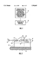
- FIG. 1 is a flow chart showing general acts in producing an array in which a cell's fixed potential dark matrix and cell electrode have overlap areas that, together with dielectric material between them, form a storage capacitor.
- FIG. 2 is schematic cross section showing a storage capacitor formed by the acts in FIG. 1.
- FIG. 3 is a flow chart showing acts that can produce a structure like that in FIG. 2.
- FIG. 4 is another flow chart showing acts that can produce a structure like that in FIG. 2.
- FIG. 5 is a schematic circuit diagram showing another layout of a cell with dark matrix connected to a fixed potential.
- FIG. 6 is a cross sectional view of the cell in FIG. 5, taken along line C--C.
- FIG. 7 is a cross sectional view of the cell in FIG. 5, taken along line D--D.
- FIG. 8 is a flow chart showing acts in producing a structure as shown in FIGS. 5-7.
- Circuitry or a “circuit” is any physical arrangement of matter that can respond to a first signal at one location or time by providing a second signal at another location or time, where the second signal includes information from the first signal. Circuitry "stores” a first signal when it receives the first signal at one time and, in response, provides the second signal at another time. Circuitry "transfers” a first signal when it receives the first signal at a first location and, in response, provides the second signal at a second location.
- Any two components are "connected” when there is a combination of circuitry that can transfer signals from one of the components to the other.
- two components are “connected” by any combination of connections between them that permits transfer of signals from one of the components to the other.
- Two components are "electrically connected” when there is a combination of circuitry that can transfer electric signals from one to the other. Two components could be electrically connected even though they are not in physical contact, such as through a combination of conductive components that are electrically connected between them.
- a “signal interval” is a period of time during which a signal is provided or received.
- An “electric circuit” is a circuit within which components are electrically connected.
- An “electric structure” is a physical structure that includes one or more electric circuits.
- a “substrate” or “chip” is a unit of material that has a surface at which circuitry can be formed or mounted.
- An “insulating substrate” is a substrate through which no electric current can flow.
- a “layer” is a thickness of material formed over a surface and extending generally parallel to the surface, with one side toward the surface and another side away from the surface.
- a layer may include two or more layers within it, referred to as “sublayers.”
- a layer may be homogeneous or its composition may vary.
- An operation "deposits" a layer by depositing material to form the layer, such as by physical or chemical vapor deposition.
- a "patterned layer” is a layer that forms a pattern.
- a patterned layer may be formed by removing part of a layer to form a pattern or by depositing a layer in a pattern.
- lithography or to “lithographically pattern” is to use a radiation source to transfer a mask pattern to a layer of radiation-sensitive material and then to develop the radiation-sensitive material to obtain a positive or negative copy of the mask pattern. If it is to be used for etching, a pattern of resist that results from development may be referred to as a "pattern of mask material” or simply a “mask.”
- An "integrated circuit” is a circuit formed at a substrate's surface by batch processes such as deposition, lithography, etching, oxidation, diffusion, implantation, annealing, and so forth.
- a "thin-film structure” is an electric structure that is formed at a surface of an insulating substrate.
- a thin-film structure could be formed, for example, by depositing and lithographically patterning films on the insulating substrate's surface.
- a part of a first layer "covers” or “has a shape that covers” or “is over” a part of a second layer if the part of the second layer is between the part of the first layer and the surface.
- a “lead” is a part of a component at which the component is electrically connected to other components.
- a “line” is a simple component that extends between and electrically connects two or more leads. A line is “connected between” the components or leads it electrically connects. A lead of a component is “connected” to a lead of another component when the two leads are electrically connected by a combination of leads and lines. In an integrated circuit, leads of two components may also be “connected” by being formed as a single lead that is part of both components.
- An “array” is an article of manufacture that includes an arrangement of "cells.”
- a "two-dimensional array” or “2D array” includes an arrangement of cells in two dimensions.
- a 2D array of circuitry may include rows and columns with a line for each row and a line for each column. Lines in one direction may be “data lines” through which a cell receives or provides signals that determine or indicate its state. Lines in the other direction may be “scan lines” through which a cell receives a signal enabling it to receive signals from or provide signals to its data line. The cell receives signals from or provides signals to a data line "under control of" a scan line if signals from the scan line enable the cell to receive signals from or provide signals to the data line.
- a cell's "addressing time" is the signal interval during which the cell's scan line enables it to receive or provide signals through its data line.
- cell circuitry is circuitry connected to a cell's scan line and data line.
- a cell is a "light active cell” if the cell includes circuitry that can interact with light, such as by sensing light, by emitting light, or by modifying reflected or transmitted light.
- the cell circuitry of a light active cell is "light active circuitry.”
- the cell's "light active area" is the area within which the cell's light active circuitry can interact with light.
- a component "blocks" light by absorbing the light or otherwise preventing the light from being transmitted or reflected.
- a "dark matrix material” is a material that can block light.
- a patterned layer of dark matrix material "blocks light in an area” if the dark matrix material blocks nearly all light in the area so that light cannot be transmitted or reflected in the area.
- a "crossing region” is a region in which two lines cross, such as a scan line and a data line.
- An “insulating layer” is a layer formed of a non-conductive material.
- a part of a layer "has an edge” if another, complementary part of the layer has been removed by one or more processes, leaving the part of the layer.
- the edge is the boundary between part of a layer and its complementary part.
- a part of a first layer "overlaps" a part of a second layer and vice versa if the part of the first layer is over and extends beyond an edge of the part of the second layer, but has an edge inside the edge of the part of the second layer.
- the "overlap area" of the first part is the area of the first part between the first part's overlapping edge and the projection of the overlapping edge of the second part onto the first part. If first and second overlapping parts are separated by a third layer, the part of the third layer that is "between" the overlapping parts is the part between the projection of the first part's overlapping edge onto the third layer and the projection of the second part's overlapping edge onto the third layer.
- An operation "forms" an electrical connection by producing an electric structure through which current can flow between components.
- the operation could, for example, solder a wire between leads of the components.
- a component is "at a fixed potential” if, during operation of the circuit, it is connected through a combination of leads and lines to a low impedance component, referred to herein as "fixed potential circuitry," that is treated as being at a fixed potential.
- fixed potential circuitry a low impedance component
- an integrated circuit typically has an external ground connection that is treated as zero potential; a component that is connected by a combination of leads and lines to the external ground connection is at a fixed potential and, more specifically, is at ground potential.
- a “capacitively coupled signal” is a signal that a component receives capacitively rather than through other events, such as flow of current to or from the component.
- a capacitively coupled signal "decays" in a material if the signal rapidly loses energy as it propagates through the material.
- a signal decays "in significantly less time than" a signal interval or other time period if the rate at which the signal loses energy is indicated by a time constant that is less than half the signal interval or other time period.
- a "connected component” is a part of a patterned layer shaped such that any two locations within the part are connected by a line of other locations within the part. Therefore, if a connected component is part of a conductive patterned layer, any two locations within the connected component are electrically connected through the connected component.
- a “capacitive element” or “capacitor” is a component that stores a voltage level by storing charge.
- a capacitive element may include two conductive components, called “electrodes,” separated by an insulating layer.
- a “dielectric layer” is an insulating layer that separates the electrodes of a capacitive element.
- a cell's area may include a "cell electrode.”
- a cell electrode may serve as one electrode of a capacitor whose other electrode is external to the array.
- Overlapping parts of two conductive layers and a part of a dielectric layer between them "form a storage capacitor" for a cell of an array if the overlapping parts and the part of the dielectric layer between them functions to capacitively store signals that are received or provided by the cell.
- the overlapping parts may, for example, be a cell electrode and a dark matrix.
- An “image” is a pattern of physical light.
- An “image output device” is a device that can provide output defining an image.
- a “display” is an image output device that provides information in a visible form.
- a “liquid crystal cell” is an enclosure containing a liquid crystal material.
- a “liquid crystal display” or “LCD” is a display that includes a liquid crystal cell with a light transmission characteristic that can be controlled in parts of the cell by an array of light control units to cause presentation of an image.
- An “active matrix liquid crystal display” or “AMLCD” is a liquid crystal display that includes a liquid crystal cell and an array of cell circuitry that can cause presentation of an image by the liquid crystal cell.
- FIGS. 1-4 show general features of the invention.
- FIG. 1 shows general acts in producing an array in which a cell's fixed potential dark matrix and cell electrode have overlap areas that, together with dielectric material between them, form a storage capacitor.
- FIG. 2 shows a storage capacitor formed by the acts in FIG. 1.
- FIGS. 3 and 4 show two ways of producing a structure like that in FIG. 2.
- the act in box 10 in FIG. 1 produces a series of layers on a surface of a substrate, with each cell including parts of the series of layers.
- the layers include a first conductive layer with scan lines, a second conductive layer with data lines, a third conductive layer with cell electrodes, a patterned layer of conductive dark matrix material, and a dielectric layer between the cell electrodes and the dark matrix.
- Each cell's dark matrix and cell electrode overlap, and the overlap areas and the dielectric material between them for a storage capacitor for the cell.
- the act in box 12 electrically connects the dark matrix to a fixed potential.
- Circuitry 40 in FIG. 2 is formed on surface 42 of substrate 44.
- Circuitry 40 includes cell electrode 50, formed in a layer of conductive material.
- Cell electrode 50 is illustratively shown over a number of other layers that could, for example, include scan lines, data lines, and a switching element for a cell, such as a TFT.
- Over cell electrode 50 are dielectric layer 52 and then dark matrix 54, a cell's part of a patterned layer of dark matrix material that is conductive. As shown, dark matrix 54 overlaps cell electrode 50.
- Capacitor 60 includes overlap area 62 of cell electrode 50, overlap area 64 of dark matrix 54, and part 66 of dielectric layer 52 between overlap areas 62 and 64. Even though dark matrix 54 is electrically connected to fixed potential circuitry 70 and is therefore held at fixed potential V F , capacitor 60 has capacitance C S , and C S can provide a cell's required storage capacitance if overlap areas 62 and 64 are large enough and if part 66 of dielectric layer 52 is thin enough. In general, a cell requires a storage capacitance that is at least two or three times as large as the capacitance of the liquid crystal in the area controlled by the cell's electrode.
- Cell electrode 50 could instead be over dielectric layer 52 and dark matrix 54, and other layers that include scan lines, data lines, and switching elements could instead be over rather than under the layers that include cell electrode 50, dielectric layer 52, and dark matrix 54.
- the act in box 80 begins by producing a series of layers that includes scan lines and data lines in first and second conductive layers, respectively, as well as insulating layers and other layers as appropriate for each cell's circuitry.
- the act in box 82 produces cell electrodes in a patterned layer of conductive material over the series of layers from box 80.
- the act in box 84 produces a dielectric pattern over the cell electrodes.
- the act in box 86 produces a conductive dark matrix pattern over the dielectric pattern, overlapping the cell electrodes to form a storage capacitor for each cell.
- the act in box 90 begins by producing a conductive dark matrix pattern.
- the act in box 92 deposits a dielectric layer over the dark matrix pattern.
- the act in box 94 produces a series of layers that includes scan lines and data lines in first and second conductive layers, respectively, as well as insulating layers and other layers as appropriate for each cell's circuitry, much as in box 80 in FIG. 3; for each cell, the act in box 94 defines a cell electrode opening in the series of layers, and the opening overlaps the cell's dark matrix.
- the act in box 96 produces cell electrodes in a patterned layer of conductive material. Each cell's electrode is in the cell's opening from box 94, so that it overlaps the cell's dark matrix to form a storage capacitor.
- FIGS. 5-8 show an implementation in which a fixed potential dark matrix overlaps with a cell electrode to form a capacitor.
- the implementation in FIGS. 5-8 can be made using AMLCD technology described in copending, coassigned U.S. Pat. No. 5,621,556, entitled “Active Matrix Liquid Crystal Device and Manufacturing Method” ("the Top ITO Application"), incorporated herein by reference.
- each pixel could be square with effective widths of approximately 45 ⁇ m ⁇ 45 ⁇ m and scan lines and data lines could be approximately 5 ⁇ m wide.
- FIG. 5 shows layout of a cell with dark matrix connected to a fixed potential.
- FIG. 6 shows a cross-section along line C--C in FIG. 5.
- FIG. 7 shows a cross-section along line D--D.
- FIG. 8 shows acts in producing a structure as shown in FIGS. 5-7.
- FIG. 5 which is a modified version of FIG. 1 of the Top ITO Application, shows a layout for a light control unit of an AMLCD.
- FIG. 5 shows three layers, with upper layers that are farthest from the substrate's surface obscuring lower layers.
- the uppermost layer shown in FIG. 5 is an ITO layer that forms transparent electrode 200.
- the next layer shown is a top metal layer, which forms data line 202 connected to one channel lead of an a-Si transistor that switches the light active circuitry.
- the top metal layer also forms line 204, which connects the other channel lead of the a-Si transistor to transparent electrode 200, and data line 206, bounding the side of the transparent electrode 200 opposite data line 202.
- the lowest layer shown is a bottom metal layer, which forms scan lines 210 and 212 bounding transparent electrode 200 and also forms lead 214, the gate lead of the transistor, which is connected to scan line 210.
- FIG. 5 does not explicitly show the dark matrix layer.
- the dark matrix layer forms a grid that is complementary to the ITO layer, overlapping the ITO layer by a distance sufficient to provide an adequate storage capacitor, such as 1 or 2 ⁇ m. Therefore, the edge of the dark matrix grid in FIG. 5 would be the same as that of transparent electrode 200, but a short distance inward. Because of the capacitor formed by the dark matrix grid and transparent electrode 200, the light control unit does not have an additional capacitor electrode. Because it covers all areas except transparent electrode 200, the dark matrix grid also covers all edges of the data lines and scan lines.
- FIGS. 6 and 7 show cross-sections along lines C--C and D--D in FIG. 5, respectively. Layers of the same material are similarly shaded and bear the same reference number in the two drawings.
- Substrate 250 has surface 252 at which a thin-film structure is formed, beginning with bottom metal layer 254 which in FIG. 6 forms scan line 210 and in FIG. 7 forms gate lead 214.
- bottom metal layer 254 Over bottom metal layer 254 is bottom nitride layer 260, followed by amorphous silicon layer 262, which in FIG. 7 includes a gated region in which the channel of a TFT can be formed.
- top nitride layer 264 Over amorphous silicon layer 262 is top nitride layer 264, forming an etch stopping island over the gated region of the amorphous silicon layer in FIG. 7.
- n + amorphous silicon layer 266 Over top nitride layer 264 where it exists and over amorphous silicon layer 262 where it is exposed elsewhere is n + amorphous silicon layer 266, providing channel leads for the TFT in FIG. 6. Over n+ layer 266 is top metal layer 268, forming data line 202 and line 204 in FIG. 7. Over top metal layer 268 is insulating layer 270, similar to the passivation layer described in the Top ITO Application but not as thick. Over insulating layer 270 is ITO layer 272, forming transparent electrode 200 in both FIGS. 6 and 7, as well as transparent electrodes of adjacent cells.
- dielectric layer 274 Over ITO layer 272 and other exposed layers is dielectric layer 274, which could be any appropriate dielectric material, such as silicon nitride, silicon oxide, or silicon oxynitride.
- dielectric layer 274 Over dielectric layer 274 is dark matrix layer 280.
- Dark matrix layer 280 could, for example, be a layer of aluminum with a black polyimide on top or on both bottom and top. Or, for easier contact at the periphery of the array, dark matrix layer 280 could be a layer of chromium with chromium oxide on both sides, also referred to as dark chromium. Because the only exposed layers after fabrication are dielectric layer 274 and dark matrix layer 280, a further passivation layer may be unnecessary in the structure of FIGS. 5-7.
- dark matrix layer 280 overlaps ITO layer 272, so that the overlap areas and the part of dielectric layer 274 between them form a storage capacitor for each cell, shown schematically with dashed lines in FIGS. 6 and 7.
- the overlap areas are sufficiently large and dielectric layer 274 is sufficiently thin that the storage capacitor provides the cell's required storage capacitance.
- the act in box 300 in FIG. 8 begins by producing a pattern in bottom metal layer 254 on an insulating substrate such as glass.
- the act in box 300 can be implemented as described in relation to FIG. 3A of the Top ITO Application, depositing chromium, molybdenum, titanium, copper-aluminum, or aluminum capped with a barrier layer of titanium, titanium-tungsten, tantalum, or any other appropriate metal or alloy.
- the act in box 300 then lithographically patterns the deposited metal to obtain a pattern that includes scan lines 210 and 212 and gate lead 214.
- bottom nitride layer 260 can be silicon nitride deposited at approximately 300°-380° C. to a thickness of approximately 3000 angstroms.
- Amorphous silicon layer 262 can contain approximately 5-12% hydrogen and can be deposited at approximately 230°-300° C. to a thickness of approximately 300-500 angstroms.
- Top nitride layer 264 can be silicon nitride deposited at approximately 200°-250° C. to a thickness of approximately 1000-1500 angstroms.
- top nitride layer 264 can also be retained in crossover regions where data lines cross scan lines, as described in copending, coassigned U.S. Pat. No. 5,486,939, entitled "Thin-Film Structure With Insulating and Smoothing Layers Between Crossing Conductive Lines," incorporated herein by reference.
- the act in box 306 deposits n + amorphous silicon layer 266 and top metal layer 268.
- the act in box 306 can be implemented as described in relation to FIG. 3C of the Top ITO Application, with n + amorphous silicon layer 266 including approximately 0.5-2% phosphorous and approximately 5-15% hydrogen, deposited at approximately 200°-250° C. to a thickness of approximately 1000 angstroms.
- Top metal layer 268 can include molybdenum-chromium, titanium, tantalum, a multilayered structure with alternating layers of aluminum and titanium-tungsten (TiW), or aluminum with appropriate barrier metal layers on top and bottom, such as titanium, TiW, or tantalum.
- a first sublayer of TiW can be approximately 500 angstroms thick; then an aluminum sublayer can be approximately 3000-10,000 angstroms thick; then a second sublayer of TiW can be approximately 500-1000 angstroms thick.
- the act in box 310 lithographically patterns top metal layer 268, n + amorphous silicon layer 266, and amorphous silicon layer 262 to produce channel leads for the transistor as well as data lines 202 and 206.
- a multiple step etch can be used after a patterned layer of photoresist has been lithographically produced, etching the second sublayer of TiW, then the aluminum sublayer, then the first sublayer of TiW, then n + amorphous silicon layer 266 and amorphous silicon layer 262, both of which will be etched by a 10:1 solution of CF 4 /0 2 .
- n + amorphous silicon layer 266 and amorphous silicon layer 262 will be retained wherever top metal layer 268 remains, including the crossover regions mentioned above in relation to box 304.
- insulating layer 270 which can include silicon oxynitride, silicon nitride, or silicon oxide, or an organic dielectric coating of polyimide or other suitable polymer layer; insulating layer 270 may be similar to the passivation layer described in relation to FIG. 3D of the Top ITO Application. For example, insulating layer 270 could be approximately 5000-50,000 angstroms thick.
- the act in box 312 patterns insulating layer 270 to produce openings through which ITO layer 272 can form electrical connections with channel leads, as between transparent electrode 200 and line 204 in FIG. 7.
- the act in box 314 then deposits and lithographically patterns ITO layer 272.
- the act in box 314 can be implemented as explained in relation to FIG. 3E of the Top ITO Application.
- ITO layer 272 forms transparent electrode 200.
- Dielectric layer 274 could include the same material as insulating layer 270, deposited under the same conditions for etching compatibility to an appropriate thickness for the required storage capacitance, such as approximately 1000-2500 angstroms.
- openings can be formed to top metal layer 268 to allow electrical connections between data lines and circuitry that provides data signals.
- openings can be formed to bottom metal layer 254 to allow electrical connections between scan lines and circuitry that provides scan signals.
- openings can be formed to allow connection of a dark matrix layer to underlying metal layers, through which it can in turn be connected to a fixed potential.
- the act in box 322 then deposits and lithographically patterns dark matrix layer 280.
- the mask used in box 320 can be the complement of that used to pattern ITO layer in box 314, with lines slightly offset to obtain an appropriate overlap for the required storage capacitance, such as approximately 1-2 ⁇ m.
- the act in box 324 electrically connects the pattern formed in dark matrix layer 280 to circuitry that provides a fixed potential.
- the electrical connection could be provided through wires or other conductive elements connected to leads in dark matrix layer 280 or in parts of other conductive layers to which it is electrically connected through one or more holes formed by the act in box 320.
- the act in box 324 may follow other acts that in turn follow box 322, such as acts that make other electrical connections.
- additional acts can be performed to assemble an AMLCD using the array. Those acts can including spinning on polyimide over dark matrix layer 280, providing further passivation.
- the implementation described above provides thin film circuitry on an insulating substrate.
- the invention could be implemented with other types of circuitry on other types of substrates.
- the above implementation provides an array of cells with particular dimensions and densities.
- the invention could be implemented with a wide variety of array sizes and shapes, cell sizes and shapes, and cell densities.
- the implementation described above includes layers in a specific sequence, but the sequence of layers could be modified.
- the above implementation has a dark matrix layer over other layers, but the invention could be implemented with a dark matrix layer under other layers, as described above in relation to FIG. 4.
- the implementation described above uses a specific cell layout and circuitry with particular materials and specific geometric and electric characteristics, but the invention could be implemented with many other layouts and types of circuitry with other materials and characteristics.
- the invention could be implemented with cell layout, circuitry, materials, and characteristics disclosed in copending, coassigned U.S. patent application Ser. No. 08/559,862, entitled “Array Having Multiple Channel Structures With Continuously Doped Interchannel Regions," incorporated herein by reference.
- the invention could be implemented with circuitry, materials, and characteristics disclosed in copending, coassigned U.S. patent application Ser. No. 08/578,780, entitled “Array With Fully Self-Aligned Amorphous Silicon TFTs,” incorporated herein by reference.
- top and bottom nitride layers include top and bottom nitride layers, but many other materials could be used in insulating layers, such as silicon oxynitride, a composite of silicon nitride and silicon oxynitride, or an anodic oxide such as tantalum oxide or aluminum oxide.
- the implementation described above includes layers of specified thicknesses, produced from specified materials by specified processes, but other thicknesses could be produced, and other materials and processes could be used.
- the dielectric layer could be thinner to increase storage capacitance.
- other semiconductor materials could be used in the semiconductor layers, including but not limited to poly-Si, microcrystalline silicon, SiGe, CdSe, or a composite layer of poly-Si and SiGe.
- various conductive materials could be used in the scan lines and data lines, including but not limited to any appropriate metal or alloy such as Al with or without layers or barrier metals, ITO, MoTa, Cr, MoCr, Ta, Cu, Ti, TiN, and any appropriate organic conductive material.
- the invention could be applied in many ways, including display arrays, light valve arrays, sensor arrays, and other arrays that interact with images.
Abstract
Description
Claims (37)
Priority Applications (3)
| Application Number | Priority Date | Filing Date | Title |
|---|---|---|---|
| US08/581,088 US5782665A (en) | 1995-12-29 | 1995-12-29 | Fabricating array with storage capacitor between cell electrode and dark matrix |
| JP31102796A JPH09197441A (en) | 1995-12-29 | 1996-11-21 | Formation of optical active cell array |
| EP96309521.1A EP0782035B1 (en) | 1995-12-29 | 1996-12-27 | Method of forming array of light active cells and array |
Applications Claiming Priority (1)
| Application Number | Priority Date | Filing Date | Title |
|---|---|---|---|
| US08/581,088 US5782665A (en) | 1995-12-29 | 1995-12-29 | Fabricating array with storage capacitor between cell electrode and dark matrix |
Publications (1)
| Publication Number | Publication Date |
|---|---|
| US5782665A true US5782665A (en) | 1998-07-21 |
Family
ID=24323840
Family Applications (1)
| Application Number | Title | Priority Date | Filing Date |
|---|---|---|---|
| US08/581,088 Expired - Lifetime US5782665A (en) | 1995-12-29 | 1995-12-29 | Fabricating array with storage capacitor between cell electrode and dark matrix |
Country Status (3)
| Country | Link |
|---|---|
| US (1) | US5782665A (en) |
| EP (1) | EP0782035B1 (en) |
| JP (1) | JPH09197441A (en) |
Cited By (24)
| Publication number | Priority date | Publication date | Assignee | Title |
|---|---|---|---|---|
| US5929948A (en) * | 1996-02-20 | 1999-07-27 | Semiconductor Energy Laboratory Co., Ltd. | Black matrix coupled to common electrode through a transparent conductive film |
| US6038004A (en) * | 1996-04-30 | 2000-03-14 | Matsushita Electric Industrial Co., Ltd. | Active matrix liquid crystal display for projection system |
| EP1037094A2 (en) | 1999-03-05 | 2000-09-20 | Sel Semiconductor Energy Laboratory Co., Ltd. | Active matrix type display device |
| US6344885B1 (en) * | 1998-04-07 | 2002-02-05 | Hitachi, Ltd. | Liquid crystal display device |
| US20020109660A1 (en) * | 1997-02-06 | 2002-08-15 | Semiconductor Energy Laboratory Co., Ltd., A Japan Corporation | Reflection type display device and electronic device |
| US6465287B1 (en) | 1996-01-27 | 2002-10-15 | Semiconductor Energy Laboratory Co., Ltd. | Method for fabricating a semiconductor device using a metal catalyst and high temperature crystallization |
| US6478263B1 (en) | 1997-01-17 | 2002-11-12 | Semiconductor Energy Laboratory Co., Ltd. | Semiconductor device and its manufacturing method |
| US6504174B1 (en) | 1996-01-19 | 2003-01-07 | Semiconductor Energy Laboratory Co., Ltd. | Semiconductor device and method for fabricating the same |
| US6528820B1 (en) | 1996-01-19 | 2003-03-04 | Semiconductor Energy Laboratory Co., Ltd. | Semiconductor device and method of fabricating same |
| US6541315B2 (en) | 1996-01-20 | 2003-04-01 | Semiconductor Energy Laboratory Co., Ltd. | Semiconductor device and fabrication method thereof |
| US6559914B1 (en) * | 2001-07-05 | 2003-05-06 | International Rectifier Corp. | Conductive black matrix layer for LCD display connected to gate through two vias |
| US6646638B1 (en) * | 1999-05-04 | 2003-11-11 | Varintelligent (Bvi) Limited | Driving scheme for liquid crystal display |
| US20030224584A1 (en) * | 2002-04-15 | 2003-12-04 | Thomas Hecht | Method and configuration for reinforcement of a dielectric layer at defects by self-aligning and self-limiting electrochemical conversion of a substrate material |
| US6690434B1 (en) | 1999-03-15 | 2004-02-10 | Semiconductor Energy Laboratory Co., Ltd. | Active matrix liquid crystal display device |
| US20040057117A1 (en) * | 2002-09-20 | 2004-03-25 | Eastman Kodak Company | Chromium black light shield |
| US6744069B1 (en) * | 1996-01-19 | 2004-06-01 | Semiconductor Energy Laboratory Co., Ltd. | Semiconductor device and its manufacturing method |
| US6795143B1 (en) * | 1999-09-22 | 2004-09-21 | Sharp Kabushiki Kaisha | Liquid crystal display device and method for manufacturing the same |
| US20050037529A1 (en) * | 2000-01-25 | 2005-02-17 | Semiconductor Energy Laboratory Co., Ltd. | Method of fabricating display device |
| US20070146265A1 (en) * | 1999-07-21 | 2007-06-28 | Semiconductor Energy Laboratory Co., Ltd. | Display device |
| US20080197354A1 (en) * | 2007-02-21 | 2008-08-21 | Kyu-Sik Cho | Thin film transistor, an organic light emitting device including the same, and a manufacturing method thereof |
| US20080266514A1 (en) * | 2007-04-25 | 2008-10-30 | Seiko Epson Corporation | Active-matrix substrate and method for producing the same, electrooptical device and method for producing the same, and electronic apparatus |
| US7709837B2 (en) | 1996-01-19 | 2010-05-04 | Semiconductor Energy Laboratory Co., Ltd | Semiconductor device and its manufacturing method |
| US20100320473A1 (en) * | 2009-01-09 | 2010-12-23 | Chih-Chung Liu | Thin film transistor structure of pixel |
| US10366660B2 (en) * | 2016-12-30 | 2019-07-30 | Shenzhen China Star Optoelectronics Technology Co., Ltd | Color filter on array (COA) substrates and liquid crystal panels |
Families Citing this family (1)
| Publication number | Priority date | Publication date | Assignee | Title |
|---|---|---|---|---|
| JP2009503572A (en) * | 2005-07-25 | 2009-01-29 | コーニンクレッカ フィリップス エレクトロニクス エヌ ヴィ | Thin film circuit having a transistor with a light-shielding body |
Citations (19)
| Publication number | Priority date | Publication date | Assignee | Title |
|---|---|---|---|---|
| EP0136509A2 (en) * | 1983-08-23 | 1985-04-10 | Kabushiki Kaisha Toshiba | Active matrix type display apparatus |
| US4568149A (en) * | 1983-01-28 | 1986-02-04 | Canon Kabushiki Kaisha | Liquid crystal display panel with opaque mask over gate or signal line |
| US4867537A (en) * | 1984-04-20 | 1989-09-19 | Hosiden Electronics Co., Ltd. | Color liquid crystal display device |
| US5056894A (en) * | 1989-03-03 | 1991-10-15 | U.S. Philips Corporation | Switching unit for a display device and display device including such a switching unit |
| JPH04280228A (en) * | 1991-03-08 | 1992-10-06 | Nec Corp | Thin film field effect type transistor driving liquid crystal display element array and driving method thereof |
| US5162933A (en) * | 1990-05-16 | 1992-11-10 | Nippon Telegraph And Telephone Corporation | Active matrix structure for liquid crystal display elements wherein each of the gate/data lines includes at least a molybdenum-base alloy layer containing 0.5 to 10 wt. % of chromium |
| EP0554061A1 (en) * | 1992-01-30 | 1993-08-04 | Canon Kabushiki Kaisha | Liquid crystal display |
| EP0556484A1 (en) * | 1991-12-25 | 1993-08-25 | Kabushiki Kaisha Toshiba | Liquid crystal display device |
| EP0569601A1 (en) * | 1991-11-29 | 1993-11-18 | Seiko Epson Corporation | Liquid crystal display and method of manufacturing same |
| EP0592063A2 (en) * | 1992-09-14 | 1994-04-13 | Kabushiki Kaisha Toshiba | Active matrix liquid crystal display device |
| EP0604006A2 (en) * | 1992-10-27 | 1994-06-29 | Nec Corporation | Active matrix liquid crystal display cell |
| US5339181A (en) * | 1991-09-05 | 1994-08-16 | Samsung Electronics Co., Ltd. | Liquid crystal display comprising a storage capacitor including the closed-ended electrode for providing a current bath for circumventing break |
| US5432625A (en) * | 1992-03-30 | 1995-07-11 | France Telecom Etablissement Autonome De Droit Public | Display screen having opaque conductive optical mask and TFT of semiconductive, insulating, and conductive layers on first transparent conductive film |
| US5486939A (en) * | 1994-04-28 | 1996-01-23 | Xerox Corporation | Thin-film structure with insulating and smoothing layers between crossing conductive lines |
| US5491347A (en) * | 1994-04-28 | 1996-02-13 | Xerox Corporation | Thin-film structure with dense array of binary control units for presenting images |
| US5510916A (en) * | 1992-01-30 | 1996-04-23 | Nec Corporation | Active matrix liquid crystal device with opposite substrate having black matrix with larger aperture than active substrate |
| US5517341A (en) * | 1992-06-01 | 1996-05-14 | Samsung Electronics Co., Ltd. | Liquid crystal display with TFT and capacitor electrodes with redundant connection |
| US5517342A (en) * | 1993-03-04 | 1996-05-14 | Samsung Electronics Co., Ltd. | Liquid crystal display having additional capacitors formed from pixel electrodes and a method for manufacturing the same |
| US5557534A (en) * | 1995-01-03 | 1996-09-17 | Xerox Corporation | Forming array with metal scan lines to control semiconductor gate lines |
Family Cites Families (2)
| Publication number | Priority date | Publication date | Assignee | Title |
|---|---|---|---|---|
| JP3098345B2 (en) * | 1992-12-28 | 2000-10-16 | 富士通株式会社 | Thin film transistor matrix device and method of manufacturing the same |
| CH689471A5 (en) | 1994-05-05 | 1999-04-30 | Landis & Gyr Tech Innovat | Summer for products of similar or different signals e.g. for electricity meter |
-
1995
- 1995-12-29 US US08/581,088 patent/US5782665A/en not_active Expired - Lifetime
-
1996
- 1996-11-21 JP JP31102796A patent/JPH09197441A/en active Pending
- 1996-12-27 EP EP96309521.1A patent/EP0782035B1/en not_active Expired - Lifetime
Patent Citations (27)
| Publication number | Priority date | Publication date | Assignee | Title |
|---|---|---|---|---|
| US4568149A (en) * | 1983-01-28 | 1986-02-04 | Canon Kabushiki Kaisha | Liquid crystal display panel with opaque mask over gate or signal line |
| US4568149C1 (en) * | 1983-01-28 | 2002-04-09 | Canon Kk | Liquid crystal display panel with opaque mask over gate or signal line |
| US4568149B1 (en) * | 1983-01-28 | 1995-12-12 | Canon Kk | Liquid crystal display panel with opaque mask over gate or signal line |
| EP0136509A2 (en) * | 1983-08-23 | 1985-04-10 | Kabushiki Kaisha Toshiba | Active matrix type display apparatus |
| US4759610A (en) * | 1983-08-23 | 1988-07-26 | Kabushiki Kaisha Toshiba | Active matrix display with capacitive light shield |
| US4867537A (en) * | 1984-04-20 | 1989-09-19 | Hosiden Electronics Co., Ltd. | Color liquid crystal display device |
| US5056894A (en) * | 1989-03-03 | 1991-10-15 | U.S. Philips Corporation | Switching unit for a display device and display device including such a switching unit |
| US5162933A (en) * | 1990-05-16 | 1992-11-10 | Nippon Telegraph And Telephone Corporation | Active matrix structure for liquid crystal display elements wherein each of the gate/data lines includes at least a molybdenum-base alloy layer containing 0.5 to 10 wt. % of chromium |
| JPH04280228A (en) * | 1991-03-08 | 1992-10-06 | Nec Corp | Thin film field effect type transistor driving liquid crystal display element array and driving method thereof |
| US5339181A (en) * | 1991-09-05 | 1994-08-16 | Samsung Electronics Co., Ltd. | Liquid crystal display comprising a storage capacitor including the closed-ended electrode for providing a current bath for circumventing break |
| EP0569601A1 (en) * | 1991-11-29 | 1993-11-18 | Seiko Epson Corporation | Liquid crystal display and method of manufacturing same |
| US5414547A (en) * | 1991-11-29 | 1995-05-09 | Seiko Epson Corporation | Liquid crystal display device and manufacturing method therefor |
| EP0556484A1 (en) * | 1991-12-25 | 1993-08-25 | Kabushiki Kaisha Toshiba | Liquid crystal display device |
| US5446562A (en) * | 1991-12-25 | 1995-08-29 | Kabushiki Kasiha Toshiba | Liquid crystal display device with transparent conductive film between pixel electrodes and signal or scanning lines |
| EP0554061A1 (en) * | 1992-01-30 | 1993-08-04 | Canon Kabushiki Kaisha | Liquid crystal display |
| US5510916A (en) * | 1992-01-30 | 1996-04-23 | Nec Corporation | Active matrix liquid crystal device with opposite substrate having black matrix with larger aperture than active substrate |
| US5432625A (en) * | 1992-03-30 | 1995-07-11 | France Telecom Etablissement Autonome De Droit Public | Display screen having opaque conductive optical mask and TFT of semiconductive, insulating, and conductive layers on first transparent conductive film |
| US5517341A (en) * | 1992-06-01 | 1996-05-14 | Samsung Electronics Co., Ltd. | Liquid crystal display with TFT and capacitor electrodes with redundant connection |
| US5459596A (en) * | 1992-09-14 | 1995-10-17 | Kabushiki Kaisha Toshiba | Active matrix liquid crystal display with supplemental capacitor line which overlaps signal line |
| EP0592063A2 (en) * | 1992-09-14 | 1994-04-13 | Kabushiki Kaisha Toshiba | Active matrix liquid crystal display device |
| US5600461A (en) * | 1992-09-14 | 1997-02-04 | Kabushiki Kaisha Toshiba | Active matrix liquid crystal display device |
| US5499123A (en) * | 1992-10-27 | 1996-03-12 | Nec Corporation | Active matrix liquid crystal display cell with light blocking capacitor electrode above insulating layer |
| EP0604006A2 (en) * | 1992-10-27 | 1994-06-29 | Nec Corporation | Active matrix liquid crystal display cell |
| US5517342A (en) * | 1993-03-04 | 1996-05-14 | Samsung Electronics Co., Ltd. | Liquid crystal display having additional capacitors formed from pixel electrodes and a method for manufacturing the same |
| US5486939A (en) * | 1994-04-28 | 1996-01-23 | Xerox Corporation | Thin-film structure with insulating and smoothing layers between crossing conductive lines |
| US5491347A (en) * | 1994-04-28 | 1996-02-13 | Xerox Corporation | Thin-film structure with dense array of binary control units for presenting images |
| US5557534A (en) * | 1995-01-03 | 1996-09-17 | Xerox Corporation | Forming array with metal scan lines to control semiconductor gate lines |
Non-Patent Citations (23)
| Title |
|---|
| Kim, S.S., Jang, I.S., Kim, D.G., and Kim, N.D., "A Fault-Tolerant Architecture for Amorphous Silicon TFT Active-Matrix LCDs," Semi Korea, Flat Panel Display Seminar, Sep. 1995, pp. 119-125. |
| Kim, S.S., Jang, I.S., Kim, D.G., and Kim, N.D., A Fault Tolerant Architecture for Amorphous Silicon TFT Active Matrix LCDs, Semi Korea, Flat Panel Display Seminar, Sep. 1995, pp. 119 125. * |
| Matsueda, Y. et al. "HDTV Poly-SI TFT-LCD Light Valve with 70% Aperture Ratio," Conference Proceedings from The 13th International Display Research Conference, Aug. 31-Sep. 3, 1993, Strasbourg, France, pp. 601-605. |
| Matsueda, Y. et al. HDTV Poly SI TFT LCD Light Valve with 70% Aperture Ratio, Conference Proceedings from The 13th International Display Research Conference, Aug. 31 Sep. 3, 1993, Strasbourg, France, pp. 601 605. * |
| Suzuki, K., "High-Aperture TFT Array Structures," SID 94 Digest, 1994, pp. 167-170. |
| Suzuki, K., High Aperture TFT Array Structures, SID 94 Digest, 1994, pp. 167 170. * |
| U.S. Patent Application No. 08/367,984 entitled "Circuitry With Gate Line Crossing Semiconductor Line at Two or More Channels", filed on Jan. 3, 1995, Now U.S. Pat. 5,608,557. |
| U.S. Patent Application No. 08/367,984 entitled Circuitry With Gate Line Crossing Semiconductor Line at Two or More Channels , filed on Jan. 3, 1995, Now U.S. Pat. 5,608,557. * |
| U.S. Patent Application No. 08/453,732 entitled "Active Matrix Liquid Crystal Device and Manufacturing Method", filed on May 30, 1995, Now U.S. Pat. 5,621,556. |
| U.S. Patent Application No. 08/453,732 entitled Active Matrix Liquid Crystal Device and Manufacturing Method , filed on May 30, 1995, Now U.S. Pat. 5,621,556. * |
| U.S. Patent Application No. 08/455,888 entitled "Integrated Dark Matrix For An Active Matrix Liquid Crystal Display And Manufacturing Method", filed on May. 31, 1995, Now U.S. Pat. 5,682,211. |
| U.S. Patent Application No. 08/455,888 entitled Integrated Dark Matrix For An Active Matrix Liquid Crystal Display And Manufacturing Method , filed on May. 31, 1995, Now U.S. Pat. 5,682,211. * |
| U.S. Patent Application No. 08/559,862 entitled "Multiple Gate Polysilicon Structures With Continuously Doped Interchannel Regions", filed on Nov. 20, 1995, Now U.S. Pat. 5,703,382. |
| U.S. Patent Application No. 08/559,862 entitled Multiple Gate Polysilicon Structures With Continuously Doped Interchannel Regions , filed on Nov. 20, 1995, Now U.S. Pat. 5,703,382. * |
| U.S. Patent Application No. 08/572,357 entitled Array With Metal Scan Lines Controlling Semiconductor Gate Lines, filed on Dec. 14, 1995, Now U.S. Pat. 5,600,155. * |
| U.S. Patent Application No. 08/577,634 entitled "Fabricating Fully Self-Aligned Amorphous Silicon Device", filed on Dec. 22, 1995, Now U.S. Pat. 5,773,804. |
| U.S. Patent Application No. 08/577,634 entitled Fabricating Fully Self Aligned Amorphous Silicon Device , filed on Dec. 22, 1995, Now U.S. Pat. 5,773,804. * |
| U.S. Patent Application No. 08/578,780 entitled "Array With Amorphous Silicon TFTS in Which Channel Leads Overlap Insulating Region No More Than Maximum Overlap (as amended)", filed on Dec. 22, 1995, Now U.S. Pat. 5,717,223. |
| U.S. Patent Application No. 08/578,780 entitled Array With Amorphous Silicon TFTS in Which Channel Leads Overlap Insulating Region No More Than Maximum Overlap (as amended) , filed on Dec. 22, 1995, Now U.S. Pat. 5,717,223. * |
| Ueda, T., Sugahara, J., Toeda, H., Akiyama, M., Ikeda, M., Suzuki, K., "A High-Aperture-Ratio TFT-LCD with a Shield-Electrode Structure," SID 93 Digest, May, 1993, pp. 739-742. |
| Ueda, T., Sugahara, J., Toeda, H., Akiyama, M., Ikeda, M., Suzuki, K., A High Aperture Ratio TFT LCD with a Shield Electrode Structure, SID 93 Digest, May, 1993, pp. 739 742. * |
| Yamanaka, H., Fukunaga, T., Koseki, T., Nagayama, K., and Ueki, T., "Integrated Black Matrix on TFT Arrays," SID 92 Digest, May 1992, pp. 789-792. |
| Yamanaka, H., Fukunaga, T., Koseki, T., Nagayama, K., and Ueki, T., Integrated Black Matrix on TFT Arrays, SID 92 Digest, May 1992, pp. 789 792. * |
Cited By (44)
| Publication number | Priority date | Publication date | Assignee | Title |
|---|---|---|---|---|
| US7709837B2 (en) | 1996-01-19 | 2010-05-04 | Semiconductor Energy Laboratory Co., Ltd | Semiconductor device and its manufacturing method |
| US6744069B1 (en) * | 1996-01-19 | 2004-06-01 | Semiconductor Energy Laboratory Co., Ltd. | Semiconductor device and its manufacturing method |
| US20030094625A1 (en) * | 1996-01-19 | 2003-05-22 | Semiconductor Energy Laboratory Co., Ltd. | Semiconductor device and method for fabricating the same |
| US7679087B2 (en) | 1996-01-19 | 2010-03-16 | Semiconductor Energy Laboratory Co., Ltd. | Semiconductor active region of TFTs having radial crystal grains through the whole area of the region |
| US6528820B1 (en) | 1996-01-19 | 2003-03-04 | Semiconductor Energy Laboratory Co., Ltd. | Semiconductor device and method of fabricating same |
| US6504174B1 (en) | 1996-01-19 | 2003-01-07 | Semiconductor Energy Laboratory Co., Ltd. | Semiconductor device and method for fabricating the same |
| US6528358B1 (en) | 1996-01-19 | 2003-03-04 | Semiconductor Energy Laboratory Co., Ltd. | Semiconductor device and method for fabricating the same |
| US6541315B2 (en) | 1996-01-20 | 2003-04-01 | Semiconductor Energy Laboratory Co., Ltd. | Semiconductor device and fabrication method thereof |
| US6465287B1 (en) | 1996-01-27 | 2002-10-15 | Semiconductor Energy Laboratory Co., Ltd. | Method for fabricating a semiconductor device using a metal catalyst and high temperature crystallization |
| US20010052954A1 (en) * | 1996-02-20 | 2001-12-20 | Semiconductor Energy Laboratory Co., Ltd. | Liquid crystal display device |
| US6198517B1 (en) * | 1996-02-20 | 2001-03-06 | Semiconductor Energy Laboratory Co., Ltd | Liquid crystal display device |
| US5929948A (en) * | 1996-02-20 | 1999-07-27 | Semiconductor Energy Laboratory Co., Ltd. | Black matrix coupled to common electrode through a transparent conductive film |
| US6038004A (en) * | 1996-04-30 | 2000-03-14 | Matsushita Electric Industrial Co., Ltd. | Active matrix liquid crystal display for projection system |
| US6478263B1 (en) | 1997-01-17 | 2002-11-12 | Semiconductor Energy Laboratory Co., Ltd. | Semiconductor device and its manufacturing method |
| US20020109660A1 (en) * | 1997-02-06 | 2002-08-15 | Semiconductor Energy Laboratory Co., Ltd., A Japan Corporation | Reflection type display device and electronic device |
| US7176993B2 (en) * | 1997-02-06 | 2007-02-13 | Semiconductor Energy Laboratory Co., Ltd. | Reflection type display device using a light shading film with a light shading material evenly dispersed throughout |
| US6344885B1 (en) * | 1998-04-07 | 2002-02-05 | Hitachi, Ltd. | Liquid crystal display device |
| EP1037094A3 (en) * | 1999-03-05 | 2001-01-03 | Sel Semiconductor Energy Laboratory Co., Ltd. | Active matrix type display device |
| EP1037094A2 (en) | 1999-03-05 | 2000-09-20 | Sel Semiconductor Energy Laboratory Co., Ltd. | Active matrix type display device |
| US6690434B1 (en) | 1999-03-15 | 2004-02-10 | Semiconductor Energy Laboratory Co., Ltd. | Active matrix liquid crystal display device |
| US6646638B1 (en) * | 1999-05-04 | 2003-11-11 | Varintelligent (Bvi) Limited | Driving scheme for liquid crystal display |
| US8362994B2 (en) | 1999-07-21 | 2013-01-29 | Semiconductor Energy Laboratory Co., Ltd. | Display device |
| US8669928B2 (en) | 1999-07-21 | 2014-03-11 | Semiconductor Laboratory Co., Ltd. | Display device |
| US8004483B2 (en) | 1999-07-21 | 2011-08-23 | Semiconductor Energy Laboratory Co., Ltd. | Display device |
| US8018412B2 (en) | 1999-07-21 | 2011-09-13 | Semiconductor Energy Laboratory Co., Ltd. | Display device |
| US7995015B2 (en) * | 1999-07-21 | 2011-08-09 | Semiconductor Energy Laboratory Co., Ltd. | Display device |
| US20070146265A1 (en) * | 1999-07-21 | 2007-06-28 | Semiconductor Energy Laboratory Co., Ltd. | Display device |
| US20070171164A1 (en) * | 1999-07-21 | 2007-07-26 | Semiconductor Energy Laboratory Co., Ltd. | Display device |
| US20070182678A1 (en) * | 1999-07-21 | 2007-08-09 | Semiconductor Energy Laboratory Co., Ltd. | Display device |
| US6795143B1 (en) * | 1999-09-22 | 2004-09-21 | Sharp Kabushiki Kaisha | Liquid crystal display device and method for manufacturing the same |
| US20050037529A1 (en) * | 2000-01-25 | 2005-02-17 | Semiconductor Energy Laboratory Co., Ltd. | Method of fabricating display device |
| US20050042798A1 (en) * | 2000-01-25 | 2005-02-24 | Semiconductor Energy Laboratory Co., Ltd. | Method of fabricating display device |
| US6559914B1 (en) * | 2001-07-05 | 2003-05-06 | International Rectifier Corp. | Conductive black matrix layer for LCD display connected to gate through two vias |
| US7176514B2 (en) * | 2002-04-15 | 2007-02-13 | Infineon Technologies Ag | Method and configuration for reinforcement of a dielectric layer at defects by self-aligning and self-limiting electrochemical conversion of a substrate material |
| US20030224584A1 (en) * | 2002-04-15 | 2003-12-04 | Thomas Hecht | Method and configuration for reinforcement of a dielectric layer at defects by self-aligning and self-limiting electrochemical conversion of a substrate material |
| US6939015B2 (en) * | 2002-09-20 | 2005-09-06 | Eastman Kodak Company | Chromium black light shield |
| US20040057117A1 (en) * | 2002-09-20 | 2004-03-25 | Eastman Kodak Company | Chromium black light shield |
| US20080197354A1 (en) * | 2007-02-21 | 2008-08-21 | Kyu-Sik Cho | Thin film transistor, an organic light emitting device including the same, and a manufacturing method thereof |
| US20080266514A1 (en) * | 2007-04-25 | 2008-10-30 | Seiko Epson Corporation | Active-matrix substrate and method for producing the same, electrooptical device and method for producing the same, and electronic apparatus |
| US8120740B2 (en) * | 2007-04-25 | 2012-02-21 | Seiko Epson Corporation | Active-matrix substrate and method for producing the same, electrooptical device and method for producing the same, and electronic apparatus |
| CN101295680B (en) * | 2007-04-25 | 2012-02-29 | 精工爱普生株式会社 | Active-matrix substrate and method for producing the same, electrooptical device and method for producing the same, and electronic apparatus |
| US20100320473A1 (en) * | 2009-01-09 | 2010-12-23 | Chih-Chung Liu | Thin film transistor structure of pixel |
| US8188518B2 (en) * | 2009-01-09 | 2012-05-29 | Century Display(ShenZhen) Co., Ltd. | Thin film transistor structure of pixel with drain extensions overlapping gate electrode and gate electrode extention |
| US10366660B2 (en) * | 2016-12-30 | 2019-07-30 | Shenzhen China Star Optoelectronics Technology Co., Ltd | Color filter on array (COA) substrates and liquid crystal panels |
Also Published As
| Publication number | Publication date |
|---|---|
| EP0782035B1 (en) | 2015-02-11 |
| JPH09197441A (en) | 1997-07-31 |
| EP0782035A1 (en) | 1997-07-02 |
Similar Documents
| Publication | Publication Date | Title |
|---|---|---|
| US5782665A (en) | Fabricating array with storage capacitor between cell electrode and dark matrix | |
| EP0762180B1 (en) | Transmissive display device | |
| US5648674A (en) | Array circuitry with conductive lines, contact leads, and storage capacitor electrode all formed in layer that includes highly conductive metal | |
| JP3654474B2 (en) | Matrix array of active matrix liquid crystal display device, liquid crystal display device and manufacturing method thereof | |
| US7522224B2 (en) | Array substrate of liquid crystal display and fabricating method thereof | |
| US6028653A (en) | Active matrix liquid crystal display panel having an improved numerical aperture and display reliability and wiring designing method therefor | |
| KR100247628B1 (en) | Liquid crystal display element and its manufacturing method | |
| US5828082A (en) | Thin film transistor having dual insulation layer with a window above gate electrode | |
| US6256077B1 (en) | Thin film transistor array panel for a liquid crystal display and a method for manufacturing the same using four photolithography steps | |
| US5933208A (en) | Liquid crystal display with color filter and light shielding layer forming a substantially planarized surface over the TFT | |
| US5231039A (en) | Method of fabricating a liquid crystal display device | |
| US5796448A (en) | Structure for a parasitic capacitor and a storage capacitor in a thin film transistor-liquid crystal display and a method for making the same | |
| US20020135710A1 (en) | Liquid crystal display device with double metal layer source and drain electrodes and fabricating method thereof | |
| KR100474529B1 (en) | Reflective liquid crystal display device and its manufacturing method | |
| US6265249B1 (en) | Method of manufacturing thin film transistors | |
| US4990460A (en) | Fabrication method for thin film field effect transistor array suitable for liquid crystal display | |
| EP0721215B1 (en) | Forming array with metal scan lines to control semiconductor gatelines | |
| KR100348995B1 (en) | The method for fabricating liquid crystal display using four masks and the liquid crystal display thereof | |
| US7705925B2 (en) | Method of manufacturing an array substrate for use in a LCD device | |
| US5929489A (en) | Display matrix structure with a parasitic transistor having a storage capacitor electrode and column electrode as source and drain regions | |
| US5693567A (en) | Separately etching insulating layer for contacts within array and for peripheral pads | |
| JPH09171196A (en) | Liquid crystal display device | |
| EP0721214A2 (en) | Circuitry with gate line crossing semiconductor line at two or more channels | |
| US5508765A (en) | Matrix-addressed type display device | |
| EP0721213B1 (en) | Array with metal scan lines controlling semiconductor gate lines |
Legal Events
| Date | Code | Title | Description |
|---|---|---|---|
| AS | Assignment |
Owner name: XEROX CORPORATION, CONNECTICUT Free format text: ASSIGNMENT OF ASSIGNORS INTEREST;ASSIGNORS:WEISFIELD, RICHARD L.;HACK, MICHAEL G.;LEVINE, JOEL;REEL/FRAME:007950/0051;SIGNING DATES FROM 19960414 TO 19960424 |
|
| STCF | Information on status: patent grant |
Free format text: PATENTED CASE |
|
| FPAY | Fee payment |
Year of fee payment: 4 |
|
| AS | Assignment |
Owner name: BANK ONE, NA, AS ADMINISTRATIVE AGENT, ILLINOIS Free format text: SECURITY INTEREST;ASSIGNOR:XEROX CORPORATION;REEL/FRAME:013153/0001 Effective date: 20020621 |
|
| AS | Assignment |
Owner name: JPMORGAN CHASE BANK, AS COLLATERAL AGENT, TEXAS Free format text: SECURITY AGREEMENT;ASSIGNOR:XEROX CORPORATION;REEL/FRAME:015134/0476 Effective date: 20030625 Owner name: JPMORGAN CHASE BANK, AS COLLATERAL AGENT,TEXAS Free format text: SECURITY AGREEMENT;ASSIGNOR:XEROX CORPORATION;REEL/FRAME:015134/0476 Effective date: 20030625 |
|
| FPAY | Fee payment |
Year of fee payment: 8 |
|
| AS | Assignment |
Owner name: XEROX CORPORATION, NEW YORK Free format text: RELEASE BY SECURED PARTY;ASSIGNOR:JP MORGAN CHASE BANK, NA;REEL/FRAME:020540/0463 Effective date: 20061204 Owner name: XEROX CORPORATION, NEW YORK Free format text: RELEASE BY SECURED PARTY;ASSIGNOR:BANK ONE, NA;REEL/FRAME:020540/0850 Effective date: 20030625 |
|
| AS | Assignment |
Owner name: XEROX CORPORATION, NEW YORK Free format text: RELEASE BY SECURED PARTY;ASSIGNOR:JP MORGAN CHASE BANK, N.A., SUCCESSOR BY MERGER TO BANK ONE NA;REEL/FRAME:021291/0203 Effective date: 20071129 |
|
| AS | Assignment |
Owner name: THOMSON LICENSING LLC, NEW JERSEY Free format text: ASSIGNMENT OF ASSIGNORS INTEREST;ASSIGNORS:XEROX CORPORATION;PALO ALTO RESEARCH CENTER INCORPORATED;REEL/FRAME:022575/0761;SIGNING DATES FROM 20080804 TO 20080805 Owner name: THOMSON LICENSING, FRANCE Free format text: ASSIGNMENT OF ASSIGNORS INTEREST;ASSIGNOR:THOMSON LICENSING LLC;REEL/FRAME:022575/0746 Effective date: 20081231 |
|
| FPAY | Fee payment |
Year of fee payment: 12 |
|
| AS | Assignment |
Owner name: XEROX CORPORATION, CONNECTICUT Free format text: RELEASE BY SECURED PARTY;ASSIGNOR:JPMORGAN CHASE BANK, N.A. AS SUCCESSOR-IN-INTEREST ADMINISTRATIVE AGENT AND COLLATERAL AGENT TO JPMORGAN CHASE BANK;REEL/FRAME:066728/0193 Effective date: 20220822 |