US5787577A - Method for adjusting an electronic part template - Google Patents
Method for adjusting an electronic part template Download PDFInfo
- Publication number
- US5787577A US5787577A US08/698,632 US69863296A US5787577A US 5787577 A US5787577 A US 5787577A US 69863296 A US69863296 A US 69863296A US 5787577 A US5787577 A US 5787577A
- Authority
- US
- United States
- Prior art keywords
- electronic part
- image
- edge
- points
- predetermined number
- Prior art date
- Legal status (The legal status is an assumption and is not a legal conclusion. Google has not performed a legal analysis and makes no representation as to the accuracy of the status listed.)
- Expired - Lifetime
Links
- 238000000034 method Methods 0.000 title claims abstract description 25
- 239000000758 substrate Substances 0.000 claims abstract description 13
- 238000005070 sampling Methods 0.000 description 5
- 230000008569 process Effects 0.000 description 3
- 230000004044 response Effects 0.000 description 2
- 235000010724 Wisteria floribunda Nutrition 0.000 description 1
- 230000008901 benefit Effects 0.000 description 1
- 230000008859 change Effects 0.000 description 1
- 230000002860 competitive effect Effects 0.000 description 1
- 238000001514 detection method Methods 0.000 description 1
- 238000010586 diagram Methods 0.000 description 1
- 238000003708 edge detection Methods 0.000 description 1
- 238000007689 inspection Methods 0.000 description 1
- 238000002372 labelling Methods 0.000 description 1
- 238000010330 laser marking Methods 0.000 description 1
- 238000004519 manufacturing process Methods 0.000 description 1
- 230000003287 optical effect Effects 0.000 description 1
- 238000003908 quality control method Methods 0.000 description 1
- 230000009467 reduction Effects 0.000 description 1
- 238000007650 screen-printing Methods 0.000 description 1
- 230000032258 transport Effects 0.000 description 1
Images


Classifications
-
- H—ELECTRICITY
- H05—ELECTRIC TECHNIQUES NOT OTHERWISE PROVIDED FOR
- H05K—PRINTED CIRCUITS; CASINGS OR CONSTRUCTIONAL DETAILS OF ELECTRIC APPARATUS; MANUFACTURE OF ASSEMBLAGES OF ELECTRICAL COMPONENTS
- H05K13/00—Apparatus or processes specially adapted for manufacturing or adjusting assemblages of electric components
- H05K13/04—Mounting of components, e.g. of leadless components
- H05K13/0404—Pick-and-place heads or apparatus, e.g. with jaws
- H05K13/0413—Pick-and-place heads or apparatus, e.g. with jaws with orientation of the component while holding it; Drive mechanisms for gripping tools, e.g. lifting, lowering or turning of gripping tools
-
- H—ELECTRICITY
- H05—ELECTRIC TECHNIQUES NOT OTHERWISE PROVIDED FOR
- H05K—PRINTED CIRCUITS; CASINGS OR CONSTRUCTIONAL DETAILS OF ELECTRIC APPARATUS; MANUFACTURE OF ASSEMBLAGES OF ELECTRICAL COMPONENTS
- H05K13/00—Apparatus or processes specially adapted for manufacturing or adjusting assemblages of electric components
- H05K13/08—Monitoring manufacture of assemblages
- H05K13/081—Integration of optical monitoring devices in assembly lines; Processes using optical monitoring devices specially adapted for controlling devices or machines in assembly lines
- H05K13/0813—Controlling of single components prior to mounting, e.g. orientation, component geometry
-
- H—ELECTRICITY
- H05—ELECTRIC TECHNIQUES NOT OTHERWISE PROVIDED FOR
- H05K—PRINTED CIRCUITS; CASINGS OR CONSTRUCTIONAL DETAILS OF ELECTRIC APPARATUS; MANUFACTURE OF ASSEMBLAGES OF ELECTRICAL COMPONENTS
- H05K13/00—Apparatus or processes specially adapted for manufacturing or adjusting assemblages of electric components
- H05K13/08—Monitoring manufacture of assemblages
- H05K13/083—Quality monitoring using results from monitoring devices, e.g. feedback loops
-
- Y—GENERAL TAGGING OF NEW TECHNOLOGICAL DEVELOPMENTS; GENERAL TAGGING OF CROSS-SECTIONAL TECHNOLOGIES SPANNING OVER SEVERAL SECTIONS OF THE IPC; TECHNICAL SUBJECTS COVERED BY FORMER USPC CROSS-REFERENCE ART COLLECTIONS [XRACs] AND DIGESTS
- Y10—TECHNICAL SUBJECTS COVERED BY FORMER USPC
- Y10T—TECHNICAL SUBJECTS COVERED BY FORMER US CLASSIFICATION
- Y10T29/00—Metal working
- Y10T29/49—Method of mechanical manufacture
- Y10T29/49002—Electrical device making
- Y10T29/49117—Conductor or circuit manufacturing
- Y10T29/49124—On flat or curved insulated base, e.g., printed circuit, etc.
- Y10T29/4913—Assembling to base an electrical component, e.g., capacitor, etc.
- Y10T29/49131—Assembling to base an electrical component, e.g., capacitor, etc. by utilizing optical sighting device
-
- Y—GENERAL TAGGING OF NEW TECHNOLOGICAL DEVELOPMENTS; GENERAL TAGGING OF CROSS-SECTIONAL TECHNOLOGIES SPANNING OVER SEVERAL SECTIONS OF THE IPC; TECHNICAL SUBJECTS COVERED BY FORMER USPC CROSS-REFERENCE ART COLLECTIONS [XRACs] AND DIGESTS
- Y10—TECHNICAL SUBJECTS COVERED BY FORMER USPC
- Y10T—TECHNICAL SUBJECTS COVERED BY FORMER US CLASSIFICATION
- Y10T29/00—Metal working
- Y10T29/49—Method of mechanical manufacture
- Y10T29/49002—Electrical device making
- Y10T29/49117—Conductor or circuit manufacturing
- Y10T29/49124—On flat or curved insulated base, e.g., printed circuit, etc.
- Y10T29/4913—Assembling to base an electrical component, e.g., capacitor, etc.
- Y10T29/49133—Assembling to base an electrical component, e.g., capacitor, etc. with component orienting
-
- Y—GENERAL TAGGING OF NEW TECHNOLOGICAL DEVELOPMENTS; GENERAL TAGGING OF CROSS-SECTIONAL TECHNOLOGIES SPANNING OVER SEVERAL SECTIONS OF THE IPC; TECHNICAL SUBJECTS COVERED BY FORMER USPC CROSS-REFERENCE ART COLLECTIONS [XRACs] AND DIGESTS
- Y10—TECHNICAL SUBJECTS COVERED BY FORMER USPC
- Y10T—TECHNICAL SUBJECTS COVERED BY FORMER US CLASSIFICATION
- Y10T29/00—Metal working
- Y10T29/53—Means to assemble or disassemble
- Y10T29/53087—Means to assemble or disassemble with signal, scale, illuminator, or optical viewer
- Y10T29/53091—Means to assemble or disassemble with signal, scale, illuminator, or optical viewer for work-holder for assembly or disassembly
Definitions
- the present invention relates generally to electronic parts and more specifically to electronic parts data used by a part placement machine to mount electronic parts on a substrate.
- a vision system including a camera prior to placement on a substrate, such as a printed circuit board, by a part placement machine.
- the vision system determines whether to discard or use each electronic part based on an image of the part and a corresponding pre-stored electronic part template.
- the electronic part template is typically provided by the supplier of the electronic part.
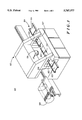
- FIG. 1 is a perspective view illustrating a part placement machine employing a vision section
- FIG. 2 is a block diagram functionally illustrating the part placement machine of FIG. 1;
- FIG. 3 is a flow chart illustrating the operation of the part placement machine of FIG. 1;
- FIG. 4 is a plan view illustrating an image of an electronic part captured by the vision section of FIG. 1;
- FIG. 5 is a plan view illustrating calculated dimensions of the image of FIG. 4.
- An apparatus for adjusting an electronic part template of an electronic part assembly system includes a memory section and a vision section.
- the memory section contains data representing the electronic part template.
- the vision section is coupled to the memory section and captures an image of the electronic part prior to placement.
- the vision section calculates one or more dimensions of the electronic part from the image.
- the data in the memory section representing the electronic part template is adjusted based on the calculated dimension.
- FIG. 1 illustrates a section of assembly line 100.
- the section of assembly line 100 includes a part placement machine 102 and a conveyance 104.
- the part placement machine 102 includes side openings 107 and 108 that permit extension of the conveyance 104 into the part placement machine 102.
- the conveyance 104 transports substrates 105, such as printed circuit boards. The substrates 105 enter the part placement machine 102 via the conveyance 104 and the side opening 107.
- the part placement machine 102 comprises a part placement section 200 (FIG. 2), a vision section 202, a control section 204, and a memory section 206.
- the control section 204 controls the operation of the part placement machine 102.
- the control section 204 comprises one or more commercially available microprocessors that execute predetermined instructions and one or more commercially available memory elements (not shown), separate from the memory section 206, that store the instructions.
- the part placement section 200 comprises tape reels 106 (FIG. 1). Each one of the tape reels 106 contains a plurality of functionally equivalent electronic parts supplied by one supplier. When a reel of parts is exhausted, the used reel is replaced by a new reel full of parts. Although the parts are functionally equivalent, the new reel may be from a different supplier. As used herein, functionally equivalent parts are those parts that are operable to substantially similar electrical specifications. The electronic parts supplied by different suppliers may have slight mechanical differences. Such mechanical differences include weight, size, composition, or the like.
- the memory section 206 comprises any suitable commercially available storage medium, such as random-access memory (RAM), floppy or magnetic disk, read/write compact disk (CD) read-only memory (ROM), or the like.
- RAM random-access memory
- CD compact disk
- ROM read-only memory
- the memory section 206 holds the data representing only one electronic part template for each type of electronic part.
- Each electronic part template defines dimensional characteristics of an electronic part, such as its length and width. Data comprising each electronic part template is manually entered into the memory section 206 to reflect the mechanical specifications of the electronic part of one supplier. Once entered, the electronic part template is not adjusted and remains in the memory section 206 until it is removed.
- the part placement section 200 includes a placement table 112 (FIG. 1).
- the placement table 112 is for positioning one or more of the substrates 105 delivered by the conveyance 104 for part placement.
- Part placement is a procedure by which the part placement machine 102 selectively removes electronic parts from the tape reels 106 and places them at predetermined locations on the substrates 105 positioned on the placement table 112.
- the control section 204 controls the part placement machine 102 to perform the procedure illustrated in FIG. 3.
- the part placement section 200 includes a placement head 110 (FIG. 1) having suction nozzles 114.
- the placement head 110 In response to instructions received from the control section 204 (FIG. 2) via bus 208, the placement head 110 (FIG. 1) directs one of the nozzles 114 to pick an electronic part from one of the tape reels 106 (at block 300 of FIG. 3).
- the vision section 202 (FIG. 2) includes a camera, such as camera 201, disposed in each of the nozzles 114 (FIG. 1) and a vision processor 203 (FIG. 2) that operates the vision section 202 in response to instructions received from the control section 204 via bus 210.
- the camera disposed in the nozzle holding the picked electronic part captures a two-dimensional image 400 (FIG. 4) of the picked electronic part (at block 302 of FIG. 3).
- the vision processor 203 which may be any suitable commercially available microprocessor, converts the image 400 from binary form into grayscale form.
- the control section 04 reads the electronic part template corresponding to the picked electronic part from the memory section 206 via bus 212 and couples it to the vision processor 203 of the vision section 202 (FIG.
- the vision processor 203 generates a tolerance window 402 (FIG. 4) based on the dimensions in the electronic part template (at block 306 of FIG. 3). In the illustrated embodiment, the vision processor 203 sets the length and width of the tolerance window 402 to be approximately 0.3 mm larger than the corresponding dimensions in the electronic part template. The vision processor 203 accepts or rejects the picked electronic part based on the fit of the image 400 within the tolerance window 402 (at block 308 of FIG. 3). If the vision processor 203 detects any points that the image 400 overlaps the tolerance window 402, a discard signal is sent to the control section 204 via bus 210. The part placement section 200 discards the picked electronic part responsive to instructions sent by the control section 204 on bus 208 (at block 310 of FIG. 3). Once discarded, the control section 204 ends the procedure of FIG. 3 (at block 312 of FIG. 3).
- the vision processor 203 does not detect any points of overlap between the tolerance window 402 (FIG. 4) and the image 400, the electronic part is accepted. If accepted, the vision processor 203 detects a predetermined number of points along the edges of the image 400 (at block 314 of FIG. 3).
- the vision processor 203 employs a known edge detection algorithm that detects edges by grayscale contrasting of the image 400 of the picked electronic part against a white background.
- the vision processor 203 initially approximates a center 403 (FIG. 4) of the image 400 based on the electronic part template.
- the vision processor 203 translates leftward along a transverse axis 405 of the image 400 from the center 403 one-half of the width defined by the electronic part template to a left edge of the image 400.
- the vision processor 203 At the left edge, the vision processor 203 generates a target window 404 and a best fit line 404a therein that describes a greatest gradient change in contrast between the left edge of the image 400 and the background.
- the vision processor 203 detects an edge point 404bat the midpoint of the best fit line 404a.
- the vision processor 203 sizes the target window 404 sufficiently large to ensure detection of the edge point 404bin situations when the image 400 is skewed because the picked electronic part held in the nozzle is rotated.
- edge point 404b may not define a midpoint of the length of the image 400, additional edge points must be calculated.
- the vision processor 203 uses the edge point 404b to generate additional edge points 406b, 408b, 410b, and 412bvia respective target windows 406, 408, 410, and 412 and respective best fit lines 406a, 408a, 410a, and 412a.
- edge points 404band 406b Once an edge point of each dimension of the image 400 is detected (i.e., edge points 404band 406b), the remaining edge points may be accurately detected with a comparatively smaller target window.
- the vision processor 203 From edge point 404b, the vision processor 203, first, translates rightward along the transverse axis 405 one-half of the width and, second, translates upward along a longitudinal axis 413 of the image 400 one-half of a length defined by the electronic part template to a top edge of the image 400. At the top edge, the vision processor 203 generates the target window 406 and best fit line 406a, and detects edge point 406b. From edge point 406b, the vision processor 203 translates downward along the longitudinal axis 413 one-quarter of the length and rightward parallel to the transverse axis 405 one-half of the width to a top right edge of the image 400.
- the vision processor 203 At the top right edge, the vision processor 203 generates the target window 408 and best fit line 408a, and detects edge point 408b. From edge point 408b, the vision processor 203 translates downward parallel to the longitudinal axis 413 one-half of the length to a bottom right edge. At the bottom right edge, the vision processor 203 generates the target window 410 and best fit line 410a, and detects edge point 410b. From edge point 410b, the vision processor 203 translates leftward parallel to the transverse axis 405 one-half of the width and downward along the longitudinal axis 413 one-quarter of the length to the bottom edge. At the bottom edge, the vision processor 203 generates the target window 412 and best fit line 412a, and detects edge point 412.
- the vision processor 203 outputs the edge points 404b, 406b, 408b, 410b, and 412bto the control section 204 (FIG. 2) via bus 210 (at block 318 of FIG. 3).
- the control section 204 determines the orientation of the picked electronic part held in the nozzle from the edge points 404b, 406b, 408b, 410b, and 412b and, accordingly, adjusts the placement head 110 (FIG. 1) of the part placement section 200 (FIG. 2) via instructions sent on bus 208 (at block 320 of FIG. 3). This ensures accurate placement of the picked electronic part.
- the vision processor 203 (FIG. 2) of the vision section 202 also calculates the dimensions of the image 400 (FIG. 5) (at block 322 of FIG. 3).
- An actual width of the image 400 is calculated in the following manner.
- the vision processor 203 generates a line segment 500 (FIG. 5) by imposing a straight line through the points 408b and 410b.
- the vision processor 203 next generates a line segment 502 by imposing a straight line, parallel to the line segment 500, through the point 406b.
- the vision processor 203 calculates the actual width of the image 400 by imposing a line segment 506 orthogonally from the line segment 500 at a point equidistant the points 408b and 410b to the line segment 502.
- the vision processor 203 defines the actual width of the image 400 as the length of line segment 506.
- An actual length of the image 400 is calculated in the following manner.
- the vision processor 203 generates a line segment 508 by imposing a straight line through the point 406b so as to intersect the line segment 500 at a right angle.
- the vision processor 203 generates a line segment 510 by imposing a straight line through the point 412b so as to intersect the line segment 500 at a right angle.
- the vision processor 203 calculates the actual length of the image 400 by imposing line segment 512 between the edge points 406b and 412b and parallel a the line segment 500.
- the vision processor 203 defines the actual length of the image 400 as the length of the line segment 512.
- the vision processor 203 outputs the calculated actual length and width of the image 400 to the control section 204 via bus 210 (at lock 322 of FIG. 3).
- the control section 204 adjusts the data representing electronic part template of the picked electronic part stored in the memory section 206 (at block 324 of FIG. 3).
- the control section 204 replaces, via bus 212, corresponding dimensions of the electronic part template stored in the memory section 206 with the newly calculated dimensions of the picked electronic part provided by the vision section 202.
- This dynamic adjustment varies the electronic part template thereby allowing variation in the size of the tolerance window 402 (FIG. 4) for subsequent ones of the same picked electronic part.
- the dynamic adjustment does not mitigate accuracy or quality in an assembly system because the electronic part template is adjusted based on electronic parts that are found to be acceptable according to prior acceptable electronic parts. This creates an electronic part template that more accurately reflects the actual, acceptable electronic parts being used and, thereby, minimizes excessive rejection rates caused by functionally equivalent, but slightly dimensionally different, electronic parts provided by different suppliers.
- the control section 204 (FIG. 2) adjusts the electronic part template in the memory section 206 only after receiving dimensions from a predetermined number, or sampling size, of the same electronic part from the vision section 202 and determining average dimensions from the predetermined sampling size.
- the control section 204 replaces corresponding dimensions of the electronic part template stored in the memory section 206 with the average dimensions.
- the control section 204 continuously repeats the process of gathering a predetermined sampling size of dimensions from the vision section 202, determining average dimensions therefrom, and storing the average dimensions in the memory section 206.
- the electronic part template reflects a statistical average of the dimensions of electronic parts within each predetermined sampling size.
- the picked electronic part is placed by the part placement section 200 on a substrate positioned on the placement table 112 (FIG. 1) (at block 326 of FIG. 3).
- the control section 204 (FIG. 2) ends the procedure (at block 312 of FIG. 3).
- the substrate exits the part placement machine 102 via the side opening 108 and the conveyance 104.
- part placement machine 102 such as, for example, a model FCP-VI manufactured and sold by Fuji Machine Manufacturing Co.
- a part placement machine 102 such as, for example, a model FCP-VI manufactured and sold by Fuji Machine Manufacturing Co.
- Fuji Machine Manufacturing Co. a part placement machine 102
- the apparatus and method described herein can find application in a variety of other machines utilized in the manufacturing environment that would benefit from dynamic adjustment of prestored dimensions of articles.
- These other machines include laser marking machines, automated optical inspection machines, screen printing machines, automated labeling machines, or the like.
- an electronic part template of an electronic part assembly system can be dynamically varied. By calculating the dimensions of the picked electronic part prior to placement, the electronic part template can be adjusted to more accurately reflect the scope of acceptable electronic parts. This permits use of functionally equivalent, but slightly dimensionally different, electronic parts provided by different suppliers without fear of excessive electronic part rejection rates and reductions in quality control.
Abstract
Description
Claims (11)
Priority Applications (1)
| Application Number | Priority Date | Filing Date | Title |
|---|---|---|---|
| US08/698,632 US5787577A (en) | 1996-08-16 | 1996-08-16 | Method for adjusting an electronic part template |
Applications Claiming Priority (1)
| Application Number | Priority Date | Filing Date | Title |
|---|---|---|---|
| US08/698,632 US5787577A (en) | 1996-08-16 | 1996-08-16 | Method for adjusting an electronic part template |
Publications (1)
| Publication Number | Publication Date |
|---|---|
| US5787577A true US5787577A (en) | 1998-08-04 |
Family
ID=24806050
Family Applications (1)
| Application Number | Title | Priority Date | Filing Date |
|---|---|---|---|
| US08/698,632 Expired - Lifetime US5787577A (en) | 1996-08-16 | 1996-08-16 | Method for adjusting an electronic part template |
Country Status (1)
| Country | Link |
|---|---|
| US (1) | US5787577A (en) |
Cited By (18)
| Publication number | Priority date | Publication date | Assignee | Title |
|---|---|---|---|---|
| US5896652A (en) * | 1996-05-08 | 1999-04-27 | Tenryu Technics Co., Ltd. | Method of packaging electronic components |
| US6016599A (en) * | 1995-11-29 | 2000-01-25 | Matsushita Electric Industrial Co., Ltd. | Device and method for mounting electronic parts |
| US6141599A (en) * | 1996-07-16 | 2000-10-31 | Kabushiki Kaisha Shinkawa | Method for setting conveying data for a lead frame |
| US6178626B1 (en) * | 1998-02-02 | 2001-01-30 | Matsushita Electric Industrial Co., Ltd. | Electronic component installation method |
| US6205636B1 (en) * | 1998-09-02 | 2001-03-27 | Matsushita Electric Industrial Co., Ltd. | Automatic assembly apparatus and automatic assembly method |
| US6332269B1 (en) | 1997-08-21 | 2001-12-25 | Micron Technology, Inc. | Component alignment methods |
| US6467162B2 (en) * | 1997-07-17 | 2002-10-22 | Fuji Photo Film Co., Ltd. | Method for mounting devices on a printed circuit board despite misalignment of resist |
| US6490787B1 (en) * | 1999-05-28 | 2002-12-10 | Ohashi Co., Ltd. | Method and apparatus for aligning and supplying electrical component |
| US20030017758A1 (en) * | 2001-06-21 | 2003-01-23 | Masayuki Arase | Apparatus for and method of mounting electronic parts |
| US6535291B1 (en) | 2000-06-07 | 2003-03-18 | Cyberoptics Corporation | Calibration methods for placement machines incorporating on-head linescan sensing |
| US6538244B1 (en) | 1999-11-03 | 2003-03-25 | Cyberoptics Corporation | Pick and place machine with improved vision system including a linescan sensor |
| US6557251B2 (en) * | 2000-03-10 | 2003-05-06 | Infotech, A.G. | Digital feature separation |
| US20030093896A1 (en) * | 2001-09-28 | 2003-05-22 | Yoshinao Usui | Electronic component mounting apparatus |
| US6608320B1 (en) | 1998-11-05 | 2003-08-19 | Cyberoptics Corporation | Electronics assembly apparatus with height sensing sensor |
| EP1424885A2 (en) * | 2002-11-29 | 2004-06-02 | Hitachi High-Tech Instruments Co., Ltd. | Electronic component mounting apparatus and electronic component mounting method |
| US20120102726A1 (en) * | 2009-06-29 | 2012-05-03 | Panasonic Corporation | Device and method for mounting electronic components |
| US20130331975A1 (en) * | 2012-06-12 | 2013-12-12 | Apple Inc. | Method and apparatus for component assembly using continuous selection |
| US20210248734A1 (en) * | 2018-05-31 | 2021-08-12 | Goertek Inc. | Method and apparatus for detecting pixel defect of optical module, and device |
Citations (5)
| Publication number | Priority date | Publication date | Assignee | Title |
|---|---|---|---|---|
| US4980971A (en) * | 1989-12-14 | 1991-01-01 | At&T Bell Laboratories | Method and apparatus for chip placement |
| US5113565A (en) * | 1990-07-06 | 1992-05-19 | International Business Machines Corp. | Apparatus and method for inspection and alignment of semiconductor chips and conductive lead frames |
| US5317802A (en) * | 1991-06-27 | 1994-06-07 | Mitsubishi Denki Kabushiki Kaisha | Method for loading a printed circuit board mounting line |
| US5384956A (en) * | 1992-07-01 | 1995-01-31 | Yamaha Hatsudoki Kabushiki Kaisha | Method for mounting components |
| US5400497A (en) * | 1990-10-29 | 1995-03-28 | Matsushita Electric Industrial Co., Ltd. | Electronic parts mounting apparatus having memory equipped parts supply device |
-
1996
- 1996-08-16 US US08/698,632 patent/US5787577A/en not_active Expired - Lifetime
Patent Citations (5)
| Publication number | Priority date | Publication date | Assignee | Title |
|---|---|---|---|---|
| US4980971A (en) * | 1989-12-14 | 1991-01-01 | At&T Bell Laboratories | Method and apparatus for chip placement |
| US5113565A (en) * | 1990-07-06 | 1992-05-19 | International Business Machines Corp. | Apparatus and method for inspection and alignment of semiconductor chips and conductive lead frames |
| US5400497A (en) * | 1990-10-29 | 1995-03-28 | Matsushita Electric Industrial Co., Ltd. | Electronic parts mounting apparatus having memory equipped parts supply device |
| US5317802A (en) * | 1991-06-27 | 1994-06-07 | Mitsubishi Denki Kabushiki Kaisha | Method for loading a printed circuit board mounting line |
| US5384956A (en) * | 1992-07-01 | 1995-01-31 | Yamaha Hatsudoki Kabushiki Kaisha | Method for mounting components |
Cited By (35)
| Publication number | Priority date | Publication date | Assignee | Title |
|---|---|---|---|---|
| US6016599A (en) * | 1995-11-29 | 2000-01-25 | Matsushita Electric Industrial Co., Ltd. | Device and method for mounting electronic parts |
| US5896652A (en) * | 1996-05-08 | 1999-04-27 | Tenryu Technics Co., Ltd. | Method of packaging electronic components |
| US6141599A (en) * | 1996-07-16 | 2000-10-31 | Kabushiki Kaisha Shinkawa | Method for setting conveying data for a lead frame |
| US6467162B2 (en) * | 1997-07-17 | 2002-10-22 | Fuji Photo Film Co., Ltd. | Method for mounting devices on a printed circuit board despite misalignment of resist |
| US7222414B2 (en) | 1997-08-21 | 2007-05-29 | Micron Technology, Inc. | Component transfer systems |
| US6332269B1 (en) | 1997-08-21 | 2001-12-25 | Micron Technology, Inc. | Component alignment methods |
| US6463653B1 (en) | 1997-08-21 | 2002-10-15 | Micron Technology, Inc. | Component alignment apparatuses |
| US6606791B1 (en) | 1997-08-21 | 2003-08-19 | Micron Technology, Inc. | Component alignment methods |
| US20050138802A1 (en) * | 1997-08-21 | 2005-06-30 | Micron Technology, Inc. | Component alignment apparatus and methods |
| US6895661B1 (en) * | 1997-08-21 | 2005-05-24 | Micron Technology, Inc. | Component alignment apparatuses and methods |
| US6845555B1 (en) | 1997-08-21 | 2005-01-25 | Micron Technology, Inc. | Component alignment methods |
| US6178626B1 (en) * | 1998-02-02 | 2001-01-30 | Matsushita Electric Industrial Co., Ltd. | Electronic component installation method |
| US6205636B1 (en) * | 1998-09-02 | 2001-03-27 | Matsushita Electric Industrial Co., Ltd. | Automatic assembly apparatus and automatic assembly method |
| US6610991B1 (en) | 1998-11-05 | 2003-08-26 | Cyberoptics Corporation | Electronics assembly apparatus with stereo vision linescan sensor |
| US6608320B1 (en) | 1998-11-05 | 2003-08-19 | Cyberoptics Corporation | Electronics assembly apparatus with height sensing sensor |
| US6490787B1 (en) * | 1999-05-28 | 2002-12-10 | Ohashi Co., Ltd. | Method and apparatus for aligning and supplying electrical component |
| US6538244B1 (en) | 1999-11-03 | 2003-03-25 | Cyberoptics Corporation | Pick and place machine with improved vision system including a linescan sensor |
| US6557251B2 (en) * | 2000-03-10 | 2003-05-06 | Infotech, A.G. | Digital feature separation |
| US20030156297A1 (en) * | 2000-06-07 | 2003-08-21 | Skunes Timothy A. | Calibration methods for placement machines incorporating on-head linescan sensing |
| US6744499B2 (en) | 2000-06-07 | 2004-06-01 | Cyberoptics Corporation | Calibration methods for placement machines incorporating on-head linescan sensing |
| US6535291B1 (en) | 2000-06-07 | 2003-03-18 | Cyberoptics Corporation | Calibration methods for placement machines incorporating on-head linescan sensing |
| US20030017758A1 (en) * | 2001-06-21 | 2003-01-23 | Masayuki Arase | Apparatus for and method of mounting electronic parts |
| US7032299B2 (en) * | 2001-06-21 | 2006-04-25 | Matsushita Electric Industrial Co., Ltd. | Apparatus for mounting electronic parts |
| US20030093896A1 (en) * | 2001-09-28 | 2003-05-22 | Yoshinao Usui | Electronic component mounting apparatus |
| US7296343B2 (en) * | 2001-09-28 | 2007-11-20 | Sanyo Electric Co., Ltd. | Electronic component mounting apparatus |
| EP1424885A3 (en) * | 2002-11-29 | 2008-01-16 | Hitachi High-Tech Instruments Co., Ltd. | Electronic component mounting apparatus and electronic component mounting method |
| EP1424885A2 (en) * | 2002-11-29 | 2004-06-02 | Hitachi High-Tech Instruments Co., Ltd. | Electronic component mounting apparatus and electronic component mounting method |
| US8646174B2 (en) * | 2009-06-29 | 2014-02-11 | Panasonic Corporation | Device and method for mounting electronic components |
| US20120102726A1 (en) * | 2009-06-29 | 2012-05-03 | Panasonic Corporation | Device and method for mounting electronic components |
| US20130331975A1 (en) * | 2012-06-12 | 2013-12-12 | Apple Inc. | Method and apparatus for component assembly using continuous selection |
| US20130326851A1 (en) * | 2012-06-12 | 2013-12-12 | Apple Inc. | Method and apparatus for component assembly using continuous selection |
| US9134724B2 (en) * | 2012-06-12 | 2015-09-15 | Apple Inc. | Method and apparatus for component assembly using continuous selection |
| US10054927B2 (en) | 2012-06-12 | 2018-08-21 | Apple Inc. | Method and apparatus for component assembly using continuous selection |
| US20210248734A1 (en) * | 2018-05-31 | 2021-08-12 | Goertek Inc. | Method and apparatus for detecting pixel defect of optical module, and device |
| US11587219B2 (en) * | 2018-05-31 | 2023-02-21 | Goertek Inc. | Method and apparatus for detecting pixel defect of optical module, and device |
Similar Documents
| Publication | Publication Date | Title |
|---|---|---|
| US5787577A (en) | Method for adjusting an electronic part template | |
| EP0660657B1 (en) | Method and mounting device for mounting a component at a specific position | |
| US6850855B2 (en) | Apparatus and method for inspecting working operations on circuit substrate, and system and method for fabricating electric circuit | |
| US6216341B1 (en) | Surface mounting method of electronic components | |
| US7346419B2 (en) | Component feeder exchange diagnostic tool | |
| US5646681A (en) | Electronic parts data recorder and a mounter employing the recorder | |
| JP4514322B2 (en) | Component mounting method and component mounting apparatus | |
| US6222629B1 (en) | Procedure and system for inspecting a component with leads to determine its fitness for assembly | |
| JP3974445B2 (en) | Mark recognition method and apparatus | |
| JP3442109B2 (en) | Electronic component mounting error correction method and component mounting device | |
| JP3691888B2 (en) | Electronic component mounting method | |
| US5038380A (en) | Method for recognizing position of component and apparatus therefor | |
| JP4707607B2 (en) | Image acquisition method for component recognition data creation and component mounter | |
| JP4681174B2 (en) | Electronic component automatic mounting device | |
| US6229608B1 (en) | Procedure and system for inspecting a component with leads to determine its fitness for assembly | |
| JP2000013097A (en) | Part mounting system | |
| JP3681843B2 (en) | Electronic component correction angle correction method and electronic component mounting apparatus using the same | |
| JP2005064026A (en) | Component mounting equipment | |
| JPH06137837A (en) | Part attitude judgement method for visual attitude selection device | |
| JPH0722800A (en) | Method of mounting electronic component and equipment for mounting electronic component | |
| JP2000106498A (en) | Part mounting method and equipment | |
| US11219148B2 (en) | Production system and production method | |
| JP2003051698A (en) | Method and device for mounting electronic component | |
| JPH07131191A (en) | Automatic electronic component mounting device | |
| JP2002057495A (en) | Electronic component mounting method |
Legal Events
| Date | Code | Title | Description |
|---|---|---|---|
| AS | Assignment |
Owner name: MOTOROLA, INC., ILLINOIS Free format text: ASSIGNMENT OF ASSIGNORS INTEREST;ASSIGNOR:KENT, KEVIN L.;REEL/FRAME:008160/0417 Effective date: 19960816 |
|
| STCF | Information on status: patent grant |
Free format text: PATENTED CASE |
|
| FPAY | Fee payment |
Year of fee payment: 4 |
|
| FPAY | Fee payment |
Year of fee payment: 8 |
|
| FPAY | Fee payment |
Year of fee payment: 12 |
|
| AS | Assignment |
Owner name: MOTOROLA MOBILITY, INC, ILLINOIS Free format text: ASSIGNMENT OF ASSIGNORS INTEREST;ASSIGNOR:MOTOROLA, INC;REEL/FRAME:025673/0558 Effective date: 20100731 |
|
| AS | Assignment |
Owner name: MOTOROLA MOBILITY LLC, ILLINOIS Free format text: CHANGE OF NAME;ASSIGNOR:MOTOROLA MOBILITY, INC.;REEL/FRAME:029216/0282 Effective date: 20120622 |
|
| AS | Assignment |
Owner name: GOOGLE TECHNOLOGY HOLDINGS LLC, CALIFORNIA Free format text: ASSIGNMENT OF ASSIGNORS INTEREST;ASSIGNOR:MOTOROLA MOBILITY LLC;REEL/FRAME:034303/0001 Effective date: 20141028 |