US5799248A - Quasi-double balanced passive reflection FET mixer - Google Patents
Quasi-double balanced passive reflection FET mixer Download PDFInfo
- Publication number
- US5799248A US5799248A US08/575,409 US57540995A US5799248A US 5799248 A US5799248 A US 5799248A US 57540995 A US57540995 A US 57540995A US 5799248 A US5799248 A US 5799248A
- Authority
- US
- United States
- Prior art keywords
- signal
- fet
- mixer
- transmission line
- terminal
- Prior art date
- Legal status (The legal status is an assumption and is not a legal conclusion. Google has not performed a legal analysis and makes no representation as to the accuracy of the status listed.)
- Expired - Lifetime
Links
- 230000008878 coupling Effects 0.000 claims abstract description 45
- 238000010168 coupling process Methods 0.000 claims abstract description 45
- 238000005859 coupling reaction Methods 0.000 claims abstract description 45
- 230000005540 biological transmission Effects 0.000 claims abstract description 38
- 230000010363 phase shift Effects 0.000 claims abstract description 9
- 239000003990 capacitor Substances 0.000 claims description 24
- 238000006243 chemical reaction Methods 0.000 claims description 15
- 229910001218 Gallium arsenide Inorganic materials 0.000 claims description 6
- 230000004044 response Effects 0.000 claims description 6
- PNEYBMLMFCGWSK-UHFFFAOYSA-N Alumina Chemical compound [O-2].[O-2].[O-2].[Al+3].[Al+3] PNEYBMLMFCGWSK-UHFFFAOYSA-N 0.000 claims description 5
- 239000000758 substrate Substances 0.000 claims description 5
- 230000006872 improvement Effects 0.000 claims description 3
- 230000001131 transforming effect Effects 0.000 claims 4
- 239000002184 metal Substances 0.000 claims 2
- 238000004804 winding Methods 0.000 claims 2
- 229910000859 α-Fe Inorganic materials 0.000 claims 2
- 238000002955 isolation Methods 0.000 abstract description 7
- 230000008859 change Effects 0.000 description 8
- 230000000903 blocking effect Effects 0.000 description 7
- 238000010586 diagram Methods 0.000 description 7
- 230000009471 action Effects 0.000 description 5
- 230000000694 effects Effects 0.000 description 4
- 230000003094 perturbing effect Effects 0.000 description 4
- 230000008901 benefit Effects 0.000 description 3
- 230000006835 compression Effects 0.000 description 3
- 238000007906 compression Methods 0.000 description 3
- 239000008186 active pharmaceutical agent Substances 0.000 description 2
- 230000004075 alteration Effects 0.000 description 2
- 230000004048 modification Effects 0.000 description 2
- 238000012986 modification Methods 0.000 description 2
- 235000014366 other mixer Nutrition 0.000 description 2
- 230000003071 parasitic effect Effects 0.000 description 2
- 238000004891 communication Methods 0.000 description 1
- 230000000295 complement effect Effects 0.000 description 1
- 150000001875 compounds Chemical class 0.000 description 1
- 238000010276 construction Methods 0.000 description 1
- 238000000586 desensitisation Methods 0.000 description 1
- 230000002708 enhancing effect Effects 0.000 description 1
- 238000002474 experimental method Methods 0.000 description 1
- 230000005669 field effect Effects 0.000 description 1
- 230000001629 suppression Effects 0.000 description 1
Images


Classifications
-
- H—ELECTRICITY
- H03—ELECTRONIC CIRCUITRY
- H03D—DEMODULATION OR TRANSFERENCE OF MODULATION FROM ONE CARRIER TO ANOTHER
- H03D9/00—Demodulation or transference of modulation of modulated electromagnetic waves
- H03D9/06—Transference of modulation using distributed inductance and capacitance
- H03D9/0658—Transference of modulation using distributed inductance and capacitance by means of semiconductor devices having more than two electrodes
- H03D9/0675—Transference of modulation using distributed inductance and capacitance by means of semiconductor devices having more than two electrodes using field effect transistors
-
- H—ELECTRICITY
- H03—ELECTRONIC CIRCUITRY
- H03D—DEMODULATION OR TRANSFERENCE OF MODULATION FROM ONE CARRIER TO ANOTHER
- H03D2200/00—Indexing scheme relating to details of demodulation or transference of modulation from one carrier to another covered by H03D
- H03D2200/0001—Circuit elements of demodulators
- H03D2200/0023—Balun circuits
-
- H—ELECTRICITY
- H03—ELECTRONIC CIRCUITRY
- H03D—DEMODULATION OR TRANSFERENCE OF MODULATION FROM ONE CARRIER TO ANOTHER
- H03D2200/00—Indexing scheme relating to details of demodulation or transference of modulation from one carrier to another covered by H03D
- H03D2200/0041—Functional aspects of demodulators
- H03D2200/0043—Bias and operating point
-
- H—ELECTRICITY
- H03—ELECTRONIC CIRCUITRY
- H03D—DEMODULATION OR TRANSFERENCE OF MODULATION FROM ONE CARRIER TO ANOTHER
- H03D2200/00—Indexing scheme relating to details of demodulation or transference of modulation from one carrier to another covered by H03D
- H03D2200/0041—Functional aspects of demodulators
- H03D2200/0066—Mixing
- H03D2200/0074—Mixing using a resistive mixer or a passive mixer
-
- H—ELECTRICITY
- H03—ELECTRONIC CIRCUITRY
- H03D—DEMODULATION OR TRANSFERENCE OF MODULATION FROM ONE CARRIER TO ANOTHER
- H03D2200/00—Indexing scheme relating to details of demodulation or transference of modulation from one carrier to another covered by H03D
- H03D2200/0041—Functional aspects of demodulators
- H03D2200/0088—Reduction of intermodulation, nonlinearities, adjacent channel interference; intercept points of harmonics or intermodulation products
-
- H—ELECTRICITY
- H03—ELECTRONIC CIRCUITRY
- H03D—DEMODULATION OR TRANSFERENCE OF MODULATION FROM ONE CARRIER TO ANOTHER
- H03D2200/00—Indexing scheme relating to details of demodulation or transference of modulation from one carrier to another covered by H03D
- H03D2200/0041—Functional aspects of demodulators
- H03D2200/009—Reduction of local oscillator or RF leakage
-
- H—ELECTRICITY
- H03—ELECTRONIC CIRCUITRY
- H03D—DEMODULATION OR TRANSFERENCE OF MODULATION FROM ONE CARRIER TO ANOTHER
- H03D7/00—Transference of modulation from one carrier to another, e.g. frequency-changing
- H03D7/12—Transference of modulation from one carrier to another, e.g. frequency-changing by means of semiconductor devices having more than two electrodes
- H03D7/125—Transference of modulation from one carrier to another, e.g. frequency-changing by means of semiconductor devices having more than two electrodes with field effect transistors
-
- H—ELECTRICITY
- H03—ELECTRONIC CIRCUITRY
- H03D—DEMODULATION OR TRANSFERENCE OF MODULATION FROM ONE CARRIER TO ANOTHER
- H03D7/00—Transference of modulation from one carrier to another, e.g. frequency-changing
- H03D7/14—Balanced arrangements
Definitions
- the invention relates generally to radio frequency communication devices and more specifically to passive transmission FET mixers requiring relatively low local oscillator power levels and having excellent isolation of the local oscillator signal relative to the radio and intermediate frequency signals.
- the dynamic range of many prior art microwave front-ends is controlled by the single and two-tone intermodulation levels of a Schottky diode mixer.
- a typical Schottky mixer obtains third order intercept points approximately equal to the local oscillator (LO) power minus the conversion loss plus 10-dB.
- the diode-ring double-balanced mixer often requires the LO power to exceed the signal compression level by 6-dB. Trade-offs between LO power levels and third order intercept and one dBm compression points are inevitable, even in multiple diode schemes attempting to improve isolation, bandwidth, and single-tone intermodulation levels.
- Weiner, et al. explain that previous designs using MESFETs had been limited by the LO balun and intermediate frequency (IF) transformer. These limitations were overcome by using a ring of GaAs MESFETs and tapered micro strip baluns in single and double balanced configurations to achieve multi-octave bandwidths. However, the bandwidth of these units is limited by the MESFET package parasitic reactances used in the ring. Weiner, et al., indicate that their future experiments will include a monolithic quad-MESFET with special gate geometry designed to improve the third order distortion, and wire-bonding of the FET to an alumina substrate to minimize parasitic reactances.
- the Siliconix Si8901-DBM is a monolithic quad-MOSFET ring demodulator/mixer that is reported to achieve third-order intercepts exceeding +37 dBm and 2-dB signal overload compression and desensitization of +30 dBm at a LO drive level of +17 dBm (50 mW).
- the Si8901 commutation-mixer relies on the switching action of the quad-MOSFET elements to effect a mixing action.
- the MOSFETs act, essentially, as a pair of switches reversing the phase of a signal at a rate determined by the LO frequency.
- the MOSFETs exhibit a finite on-resistance that is expressed as a conversion efficiency loss.
- the loss results from the r ds (on) of the MOSFETs relative to both the signal and IF impedances and signal conversion to unwanted frequencies.
- the present invention comprises a quasi-double balanced passive reflection FET mixer that operates with reduced levels of nonlinearity and intermodulation distortion as the result of the topological structure and the application of a dc bias to FET channels used for mixing which is useful for both up- and down-frequency conversion of non-overlapping RF and IF signal frequencies.
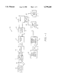
- FIG. 1 is a block diagram of an embodiment of the quasi-double balanced mixer of the present invention.
- FIG. 2 is a schematic diagram of a preferred embodiment of the quasi-double balanced mixer of the present invention.
- FIG. 3 is a schematic of a pair of back-to-back FETs used as a model to explain how the present invention reduces intermodulation distortion in the preferred embodiment.
- FIG. 4 is a schematic diagram showing propagarion of a wavefront in a transmission line.
- FIG. 5 is a schematic diagram of the embodiment of the invention in FIG. 2 showing the incident wavefront propagation and current flow in the mixer when FETs Q1 and Q2 are conducting (ON) or non-conducting (OFF).
- FIG. 6 is a schematic diagram of the embodiment of the invention in FIG. 2 showing the reflected wavefront propagation and current flow in the mixer when FETs Q1 and Q2 are non-conducting (OFF).
- FIG. 7 is a schematic diagram of the embodiment of the invention in FIG. 2 showing the reflected wavefront propagation and current flow in the mixer when FETs Q1 and Q2 are conducting (ON).
- Mixer 10 comprises a local oscillator (LO) input circuit 11, a switching circuit 12 coupled to local oscillator circuit 11 via filter circuit 13 (a D.C. blocking circuit in the preferred embodiment), a switching circuit control circuit 14 coupled to and provided for controlling the switching of the switching circuit 12, a radio frequency (RF) port to intermediate frequency (IF) port coupling circuit 16 (an RF-to-IF Balun circuit in the preferred embodiment) connected to the switching circuit 12, and a diplexer circuit 23 coupled between the RF-to-IF coupling circuit 16 and RF port 24 and IF port 28.
- Switching circuit 12 acts as the LO/RF or LO/IF signal mixer by creating a time varying impedance that varies in response to the applied LO signal.
- a two-terminal local oscillator port 19 having a pin terminal 20 and a ground terminal 21 is provided for coupling an external local oscillator signal source 22 to the local oscillator input circuit 11.
- a two-terminal radio frequency (RF) port 24 having a pin terminal 25 and a ground terminal 26 is provided for coupling an external radio frequency signal source (or sink) 27 to the RF-to-IF coupling circuit 16 via diplexer circuit 23.
- a two-terminal intermediate frequency (IF) port 28 having a pin terminal 29 and a ground terminal 30 is provided for coupling an external intermediate frequency signal load/sink (or source) 31 to RF-to-IF coupling circuit 16 via diplexer 23.
- Control circuit 14 may optionally be provided with a control circuit input port 32 for coupling the control circuit to an external control signal generator 33.
- Switching circuit 12 is a three port device having a LO signal input port 17 for receiving the LO signal which functions to operate the switch, and first and second ports coupled to the RF and IF ports 24, 28 through the RF-to-IF (IF-to-RF) coupling circuit 16 and diplexer circuit 23.
- the switching circuit responds to the applied LO signal by turning ON and OFF at the LO signal frequency, thereby causing a rapid time-varying change in resistance of the switching elements.
- Unbalanced diplexer circuit 23 functions to filter and separate the IF from the RF signals during either up-frequency conversion in which an IF signal is applied (source) and an RF signal is extracted (sink or load) or down-frequency conversion in which an RF signal is applied (source) and the IF signal is extracted (sink or load).
- RF-to-IF (IF-toe RF) coupling circuit 16 functions to prevent LO signals from appearing at the RF and IF ports, and to transform the RF and IF signal impedance.
- FIG. 2 is an illustration of a preferred embodiment of the quasi-double balanced mixer shown in functional block diagram form in FIG. 1.
- the term "quasi-double balanced" is used in describing the inventive mixer 10 because the inventive mixer 10 resembles a double balanced mixer in that both RF and IF ports are balanced via coupling circuit 16, and resembles a single balanced mixer in that RF and IF signals must be non-overlapping in frequency.
- This embodiment nominally operates over a LO/RF frequency range of from about 800 MHz to about 1000 MHz, but there are no absolute limits to the useful frequency range of the inventive mixer.
- the illustrated embodiment of the mixer nominally operates with a LO drive of about +17 dBm and about a +5 Volt drain bias voltage.
- the gate terminals are self biasing at about -2 volts.
- switching device 12 is realized with a pair Q1 38 and Q2 39 of interconnected field-effect transistors (FETs), each FET having a control or gate (G) terminal, as well as drain (D) and source (S) terminals.
- the source terminal of Q1 is connected to the source terminal of Q2.
- the FET-pair switching device 12 is responsible for mixing the local oscillator (LO) signal coupled to the FET switch by the LO input circuit 11 with the radio frequency (RF) signal coupled to the FET switch by the RF-to-IF coupling circuit 16 and Diplexer Circuit 23 to generate an intermediate frequency (IF) signal.
- LO local oscillator
- RF radio frequency
- FET-pair (Q1-Q2) is at the heart of the signal mixing action and couples to the LO, RF, and IF functional components of the mixer circuit 10, the structure and operation of mixer 10 are described relative to the FET-pair Q1 38 and Q2 39.
- FET pair Q1-Q2 provides a single switching operation between circuit nodes 40 and 41, each of which nodes corresponds to a drain terminal of one of the FETs. In this embodiment, both interconnected FET source terminals are connected to ground.
- signal propagation through a FET junction has a perturbing effect on FET admittance (or resistance) which results in FET output signal distortion, particularly signal intermodulation distortion when the FET is used as a signal mixing means. Therefore, reducing the admittance (resistance) perturbing effect reduces distortion and improves overall mixer performance.
- implementing the signal switching function with a FET-pair rather than with a single FET reduces the perturbing effect on admittance as described hereinafter, and results in reduced distortion.
- the RF signals are forced to pass through both FETs (Q1 38 and Q2 39) in such a way that the RF signal enters the drain of one FET (Q1) at circuit node 40 emerges from the source terminal of the same FET (Q1) at circuit node 62, then enters the source terminal of the second FET (Q2) and emerges from the drain of the second FET (Q2) at circuit node 41.
- propagation of the RF signal through the first FET (Q1) drain-to-source may perturb the admittance of the FET with the resulting effect on the signal, but for FETs (Q1 and Q2) of comparable construction, propagation through the second FET (Q2) source-to-drain has an opposite perturbing effect on the admittance of Q2 as compared to the effect on Q1.
- the net effect of propagation of the signal through both serially connected (source-to-source) FETs Q1 and Q2 is cancellation of some of the distortion, including an appreciable amount of intermodulation distortion.
- the FETs operate with a gate bias voltage Vg applied by gate bias circuit 48 between the gate and source terminals and a drain bias voltage Vd applied by drain bias circuit 45 between the drain and source terminals.
- the drain bias voltage is generated by an external drain bias voltage source 46, while the gate terminals of the FETs are self biased.
- FIG. 3 shows a pair of serially connected FETS.
- the serially connected FET-pair structure, and application of drain bias to the channels of the FET transistors significantly reduce the intermodulation distortion in the mixer output signal.
- FIG. 3 is a simplified circuit which illustrates how the back-to-back connected FETs (Q1-Q2) cancels intermodulation distortion.
- the gate-to-source voltage (V GS ) is equal to the sum of the gate-to-drain voltage (V GD ) and the drain-to-source voltage (V DS ).
- V GS be fixed, set by a fixed voltage source for example, then: ##EQU1## where ⁇ R DS is the change in resistance between the FET drain and source terminals.
- the change in resistance between the two FET drains ( ⁇ R D1D2 ) is equal to the change of resistance between the source and drain of the first FET Q1 ( ⁇ R D1S1 ) and the change of resistance between the source and drain of the second FET Q2 ( ⁇ R D2S2 ).
- V D1D2 is symmetrically dropped across both FETS Q1 and Q2, so that:
- FET pair Q1-Q2 is pumped by LO circuit 11 comprising inductor L1 46 (15 nH) , resistor R1 47 (100 ohm), and capacitor C1 44 (50 pF) which may alternatively be considered a component of filter 13 rather than as a component of LO input circuit 11.
- Inductor L1 46 and resistor R1 47 are connected in parallel with each other across the LO input port 19 and therefore in parallel with the external oscillator source 22, while capacitor C1 44 is serially connected between the local oscillator source 22 and the gate terminals of the FET-pair. Inductor L1, capacitor C1, and resistor R1 also for the gate bias circuit 48 as described.
- Intrinsic gate capacitances of the FET transistors Q1 and Q2 are tuned to an open circuit with inductor L1 46.
- Resistor R1 47 provides the necessary matching load impedance to the local oscillator input port 19.
- Capacitor C1 44 is a dc blocking capacitor which allows the gates of FET-pair Q1-Q2 to self bias at about -2 volts.
- RF port 24 and IF port 28 are coupled to mixer 10 through an unbalanced diplexer circuit 23 comprising inductor L2 51 (36 nh), capacitor C4 52 (10 pF), and capacitor C5 53 (10 kpF).
- the unbalanced diplexer circuit 23 is then coupled to the balanced FET-pair switching circuit comprising FETS Q1-Q2 via transmission line balun T1 72 (comprising T1A 73 and T1B 74).
- Balun T1 72 acts to prevent LO frequency signals appearing at the FET drain terminals of Q1 and Q2 from coupling to the RF and/or IF ports.
- LO signal coupling to the RF and/or IF ports is prevented because equal LO voltages at circuit nodes 40, 41 cancel at node 63 by the symmetry of balun T1.
- Balun T1 72 also acts to transform the RF input signal impedance from about 50 ohms to about 200 ohms.
- the mixing FETs provide a more ideal short circuit to a 200 ohm system than to a 50 ohm system so that the conversion efficiency is improved.
- the mismatched impedance results in reflection of the signal, and the reflected signal is then transformed in reverse propagation from the FET drains through balun T1 into 50 ohms.
- Mixer 10 operates as a passive reflection mixer even though balun T1 72 does not operate as reflection transformer.
- Intermodulation distortion is significantly reduced by the application of a dc drain bias voltage to the channels of mixing FETs Q1 and Q2.
- External bias voltage (+5V) is applied to bias port 32 and processed through drain bias circuit 45 comprising optional diode D1 50, and resistor R2 51, capacitor C2 52, and capacitor C3 54.
- Capacitors C4 52, C5 53, C6 59, and C7 57 provide dc blocking (among other functions) so as to force bias current through the FETs.
- Diode D1 50 provides reverse bias protection and is optionally provided in the mixer circuit 10.
- Resistor R2 51 (100 ohms) provides current limiting to while the combination of resistor R2 51 and capacitor C2 52 work together with balun T1 72 to provide the appropriate RF impedance to the drains of the FETs.
- Capacitor C3 54 provides ac isolation of bias port 32 from other components of mixer circuit 10.
- the drain bias circuit 45 feeds the center tap node 60 of balun T1 72 which in turn supplies drain bias current to the FET-pair drain terminals.
- a dc drain bias voltage is generated by dc drain bias circuit 45 and applied to the channels of the mixing FETs (Q1, Q2) at each FET drain terminal. This drain bias voltage to the FET pairs significantly reduces intermodulation distortion in the output signal.
- Drain bias circuit 45 is connected to an external dc bias voltage source 46 at drain bias port 32.
- Scaling resistor R2 (100 ohm) 51 serves to scale the bias voltage that appears at the drain terminal of each FET transistor (Q1, Q2), and to limit the bias current through each FET.
- the combination R2 51 and C2 52 provide the bias source circuit with the proper RF impedance.
- Optional diode D1 50 provides reverse bias protection.
- Capacitor C3 54 provides ac isolation of the bias port 32 from the other mixer components.
- the drain bias voltage is coupled to each FET drain terminal through resistor R2 to circuit node 60 and through baluns T1A 73 and T1B 74 to the FET drain.
- balun T1 72 provides a dc path for the drain bias current.
- bias for Q2 flows from the output of resistor R2 51, into balun wire T1A2 at circuit node 60, into balun wire T1B2 at circuit node 61, into the drain terminal of Q2 at node 41, out the source terminal of Q2, and to ground at circuit node 62.
- Bias for Q1 flows from the output of resistor R2 51, into balun T1B1 at circuit node 60, into balun T1A1 at circuit node 63, into the drain terminal of Q1 at node 40, and, out the source terminal of Q1, at node 62 to ground.
- each FET also advantageously causes each FET to function as a LO signal amplifier.
- a drain bias voltage is applied to the FET drain terminals, and the LO signal is applied to the connected gate terminals of the paired FETs, a LO response signal appearing much like an amplified version of the gate terminal LO signal is generated within the FET structure and appears at each conducting FET drain terminal.
- the appearance of this drain LO response signal enhances the switching behavior of the FET.
- the applied LO signal and the response LO signal generated within the FET junction work together in a compound fashion so that, in essence, each FET sees a larger LO driving signal than the LO signal applied at the gate alone. Therefore, the FET switches operate with a lower externally applied LO signal.
- the gate terminal is self-biased so that no explicit gate bias supply is needed.
- Gate bias voltage is generated for the FET pair (Q1-Q2) 38, 39 by coupling capacitor C1 44, which functions as a dc current blocking capacitor, between the LO input circuit 11 and FET-pair Q1 and Q2 gate terminals.
- Each of FETS Q1 and Q2 attains to a self bias level of about -2 volts by the charging of capacitor C1 44 during forward conduction of the FET gate junctions.
- Eliminating an explicit bias source for the gate is advantageous because such implementation reduces cost by eliminate some components, and eliminates the inconvenience of having to provide the separate bias source. Provision of self-biasing circuitry does not preclude application of a separate external gate bias if additional flexibility is desired for tuning the behavior of the mixer circuit 10.
- balun T1 comprises a pair of 100 ohm transmission line bifilar wires.
- the RF and IF ports 24, 28 are coupled to each other via balun T1 transformers 73, 74 in such a fashion that (for example) during frequency down-conversion, and in conjunction with a LO signal applied to the FET switches 38, 39, RF signal input energy flows from the RF port 24 (source) to the IF port 28 (sink).
- balun T1 participates in the conveyance of energy during each and every LO signal half cycle.
- the energy (current) flow is achieved by providing direct electrical connections between appropriate circuit components (as shown and described) and by exciting modes in the transmission line balun T1 that have appropriate propagation modes.
- the RF to IF coupling circuit 16 includes an input port having first 42 and second 43 primary-port terminals, and first 40 and second 41 secondary port terminals. The terms primary and secondary are selected because in a sense both ports of the coupling network serve as both "input” and “output” terminals depending on which signal is of concern.
- RF port pin terminal 25 is connected to capacitor C4 52 (10 pF) which in turn is connected to balun T1 (T1A1 73) at circuit node 63.
- the serial combination of inductor L2 51 (36 nH) and capacitor C6 59 (10 pF) is also connected from circuit node 63 to the RF port ground terminal 64 (a terminal shared with the IF port 28).
- Capacitor C7 57 (10K pF) is connected between the RF port ground terminal 64 and balun T1 (T1B2).
- the IF port pin terminal 29 is coupled to the common circuit node of the serial combination of L2 51 and C6 59, via dc blocking capacitor C5 53.
- Balun T1 72 is coupled between circuit nodes 61 and 62 and the FET drains at nodes 40 and 41. More specifically, T1A1 is directly electrically connected between node 63 and node 40, balun T1B2 is directly electrically connected between node 61 and node 41, and the serial combination of balun sections T1B1 and T1A2 is directly electrically connected between nodes 61 and 63. At the same time, transformers T1A1 and T1A2 are magnetically coupled and transformers T1B1 and T1B2 are magnetically coupled.
- This electrical and magnetic coupling acts to prevent LO frequency signals which appear at the FET drain terminals from coupling to the RF and/or IF ports, and to transform the RF input signal to a 200 ohm system so that the mixing FETs Q1-Q2 provide a more ideal short circuit during their conduction phase.
- Q1 and Q2 are in phase, that is, they are both ON during one half cycle of the LO signal, and both OFF during other LO signal half cycle.
- the energy in a wave travels in a single direction (before reflection), in this case from left to right as shown in FIG. 4.
- the symbol indicating an impedance (e.g. 50 ⁇ ) a direction arrow (e.g. ⁇ ) and a polarity (+ -) indicate respectively the impedance, the propagation direction of the traveling wave, and the polarity of the wave relative to the propagation direction.
- impedance e.g. 50 ⁇
- a direction arrow e.g. ⁇
- a polarity (+ -) indicate respectively the impedance, the propagation direction of the traveling wave, and the polarity of the wave relative to the propagation direction.
- a pair of associated local currents exists in the line at X 0 , where the local currents flow in complementary directions, as shown.
- the wave is partially reflected, resulting in both forward and reflected traveling waves at the load. It is the local current pairs of the forward and reflected waves that flow through the load.
- the traveling voltage wave reflects from the FETs due to impedance mismatch between the transmission line ( ⁇ 50 ⁇ ) and the FETS (Z FETS ,ON ⁇ 8 ⁇ , Z FETS ,OFF 1000 ⁇ ).
- Z FETS the FET impedance is much less than the line impedance (Z FETS ⁇ 50 ⁇ ) and when the FETS are not conducting, their impedance is much greater that the line impedance (Z FETS >>50 ⁇ ).
- the current associated with the local wavefronts of both the incident and reflected waves must flow through Q 1 , and Q 2 , since they form current pairs flowing into the load (e.g. at node A) and out of the load (e.g. at node B); hence they flow through the load.
- the LO input signal pumps the FETs and either turns both ON or both OFF.
- FET transistors Q1 and Q2 do not operate in their linear regions for any significant time and will either be fully ON or fully OFF.
- FETs Q1 and Q2 present a low impedance (typically about 8 ohms) when conducting (ON) and a very high impedance (greater than 1000 ohms) when not conducting (OFF), and either way they do not present an impedance comparable to the impedance of the baluns (generally about 200 ohms in this embodiment).
- the mixing function is now described in terms of traveling voltage waves.
- incident RF voltage at RF-port propagates into mixer 10 in the form of a traveling voltage wave (from right-to-left as shown if FIG. 5) after having passed through diplexer capacitor C4 52 and dc blocking capacitor C7 57.
- the traveling wave has a characteristic impedance of 50 ⁇ .
- the resulting waves each have a characteristic impedance of 100 ⁇ .
- the 100 ⁇ waves emerge from the ends (the left ends as shown in FIG. 5) of T1A and T1B where the waves recombine. Since the two transmission lines are connected in series at the point the waves emerge, it is the voltage of these waves that combines, resulting in a characteristic impedance of 200 ⁇ .
- FIG. 6 pertains to operation when FETs Q1 and Q2 are nonconducting (OFF), while FIG. 7 pertains to operation when FETs Q1 and Q2 are conducting (ON).
- Q1 and Q2 are OFF, the 200 ⁇ traveling wave sees a high impedance line termination (Z L >>2000 ⁇ ), resulting in nearly complete reflection of energy at the FETs (impedence mismatch and reflection shown symbolically by the dotted line) with no phase shift.
- the 200 ⁇ reflected wave now travels from left to right (as shown in FIG. 6) and enters T1A and T1B. Since the two transmission lines are connected in series at the point the wave enters the, it is the voltage that splits equally between the lines.
- 100 ⁇ waves travel in each of T1A and T1B as shown.
- the waves emerge from T1A, T1B and recombine. Since the transmission lines are connected in parallel where the waves emerge, it is the current of each wave that combines or sums. This combination results in a 50 ⁇ traveling wave at the diplexer, whose phase is that of the input RF wave (neglecting phase shift across the various transmission lines of the mixer).
- operation is similar to that described above, except that when the FETS are ON, the FETS have resistance approximately equal to 80 ⁇ and 8 ⁇ 200 ⁇ . Therefore, nearly all of the incident energy at the FETs is reflected, and the phase of the wave is shifted 180° since load impedance Z L ⁇ 200 ⁇ . This appears as a voltage polarity reversal in the figures. Furthermore, the traveling wave appearing at the diplexer is now phase shifted relative to the RF input wave by 180° (again neglecting phase shift across the transmission lines in the mixer).
- the reflected wave is commutated with each half cycle of the LO signal, and the reflected wave contains LO-RF, and LO+RF frequencies. Since nearly all of the RF input traveling wave is reflected from FETs in each case (FETs ON or OFF), commutation is nearly symmetric, resulting in cancellation of the RF component of the reflected wave. Only the LO-RF or the RF-LO (whichever gives a positive number) can pass through low pass filter section (L2, C6) of the diplexer. The signal also passes through dc blocking capacitors C5 and C7, and appears at the IF port in the form of a 50 ⁇ output signal.
- L2, C6 low pass filter section
- the RF-to-IF coupling balun provides at least four benefits.
- the balun T1 72 cooperates with other mixer components to provide the mixing and energy coupling function of the mixer circuit.
- the balun is an important component of the drain bias circuit.
- the balun acts to transform the RF input signal impedance to 200 ohms; the mixing FETs provide a much more ideal short circuit to a 200 ohm system, thereby yielding a improvement in conversion efficiency.
- the reflected IF signal is transformed in reverse propagation (reflection) through the balun to 50 ohms.
- Each of the RF and IF ports 24, 28 are band-limited.
- Mixer 10 operates in the manner described only when the RF and IF signal frequencies are separated and do not overlap.
- the typical range of RF frequencies is between about 800 MHZ and about 1000 MHz
- the typical range of IF frequencies is between about 10 MHZ and about 100 MHz, however, other there is no absolute limit to the useful range of signal frequencies in the inventive mixer.
- the RF and IF bands are preferably separated by at least about 2 octaves to maintain isolation.
- Mixer 10 may be used for up-conversion in which case the input energy is injected into the IF port, or it may be used for frequency down-conversion in which case the input energy is injected into the RF port.
- mixer circuit 10 may be used for frequency up-conversion by applying an intermediate frequency signal to IF port 28 and extracting an up-converted RF signal at RF port 24.
- the RF and IF frequency bands may be distinct and non-overlapping.
Abstract
Description
V.sub.GS =V.sub.GD +V.sub.DS
V.sub.D1S1 =-V.sub.D2S2 (approximately).
ΔR.sub.D1D2 ≅0.
Claims (24)
Priority Applications (3)
| Application Number | Priority Date | Filing Date | Title |
|---|---|---|---|
| US08/575,409 US5799248A (en) | 1995-12-20 | 1995-12-20 | Quasi-double balanced passive reflection FET mixer |
| PCT/US1996/020548 WO1997023036A1 (en) | 1995-12-20 | 1996-12-18 | Quasi-double balanced passive reflection fet mixer |
| AU13469/97A AU1346997A (en) | 1995-12-20 | 1996-12-18 | Quasi-double balanced passive reflection fet mixer |
Applications Claiming Priority (1)
| Application Number | Priority Date | Filing Date | Title |
|---|---|---|---|
| US08/575,409 US5799248A (en) | 1995-12-20 | 1995-12-20 | Quasi-double balanced passive reflection FET mixer |
Publications (1)
| Publication Number | Publication Date |
|---|---|
| US5799248A true US5799248A (en) | 1998-08-25 |
Family
ID=24300205
Family Applications (1)
| Application Number | Title | Priority Date | Filing Date |
|---|---|---|---|
| US08/575,409 Expired - Lifetime US5799248A (en) | 1995-12-20 | 1995-12-20 | Quasi-double balanced passive reflection FET mixer |
Country Status (3)
| Country | Link |
|---|---|
| US (1) | US5799248A (en) |
| AU (1) | AU1346997A (en) |
| WO (1) | WO1997023036A1 (en) |
Cited By (19)
| Publication number | Priority date | Publication date | Assignee | Title |
|---|---|---|---|---|
| US6108529A (en) * | 1998-02-01 | 2000-08-22 | Bae Systems Aerospace Electronics Inc. | Radio system including FET mixer device and square-wave drive switching circuit and method therefor |
| US6163689A (en) * | 1997-09-30 | 2000-12-19 | Samsung Electronics Co., Ltd. | Negative self-bias circuit for FET mixers |
| US20020106996A1 (en) * | 2001-01-30 | 2002-08-08 | Jens-Peer Stengl | Method and device for transferring a signal from a signal source to a signal sink in a system |
| US20030157918A1 (en) * | 2002-02-20 | 2003-08-21 | Doron Gamliel | Double balanced FET mixer with high IP3 and IF response down to DC levels |
| US6614848B2 (en) * | 1995-11-22 | 2003-09-02 | Schleifring Und Apparatebau Gmbh | Device for transmitting signals between moving parts |
| US6871059B1 (en) * | 1999-06-16 | 2005-03-22 | Skyworks Solutions, Inc. | Passive balun FET mixer |
| US6900711B2 (en) | 2002-09-30 | 2005-05-31 | Agilent Technologies, Inc. | Switching system |
| US20070072576A1 (en) * | 2003-04-01 | 2007-03-29 | Henrik Sjoland | Passive mixer |
| US20090189673A1 (en) * | 2008-01-24 | 2009-07-30 | Avago Technologies Wireless Ip (Singapore) Pte, Ltd. | Mixer with balanced local oscillator signal |
| US7580693B2 (en) | 2004-10-27 | 2009-08-25 | Synergy Microwave Corporation | Passive reflection mixer |
| US20100232255A1 (en) * | 2006-06-05 | 2010-09-16 | The University Of Bristol | Mixing apparatus and method of designing a mixing apparatus |
| US20120218223A1 (en) * | 2011-02-25 | 2012-08-30 | Maxim Integrated Products, Inc. | Continuous time correlator architecture |
| US8264283B1 (en) | 2007-03-29 | 2012-09-11 | Scientific Components Corporation | Single side band mixer |
| US8344818B1 (en) | 2007-06-15 | 2013-01-01 | Scientific Components Corporation | Single side band (SSB) mixer |
| US8670741B2 (en) | 2011-12-21 | 2014-03-11 | Triquint Semiconductor, Inc. | Mixer with high second-order and third-order intercept point |
| JP2016086417A (en) * | 2014-10-27 | 2016-05-19 | 島田理化工業株式会社 | Frequency mixer, frequency converter, signal quality measurement system, and transmitter |
| US9552102B2 (en) | 2011-02-25 | 2017-01-24 | Qualcomm Incorporated | Background noise measurement and frequency selection in touch panel sensor systems |
| US9846186B2 (en) | 2011-02-25 | 2017-12-19 | Qualcomm Incorporated | Capacitive touch sense architecture having a correlator for demodulating a measured capacitance from an excitation signal |
| DE102009049609B4 (en) | 2008-10-17 | 2018-08-16 | Infineon Technologies Ag | Stripline balun |
Families Citing this family (1)
| Publication number | Priority date | Publication date | Assignee | Title |
|---|---|---|---|---|
| SE541484C2 (en) * | 2018-03-05 | 2019-10-15 | Chalmers Ventures Ab | Balanced resistive frequency mixer |
Citations (11)
| Publication number | Priority date | Publication date | Assignee | Title |
|---|---|---|---|---|
| US3700928A (en) * | 1969-07-30 | 1972-10-24 | Westinghouse Electric Corp | Fast pulldown transmission line pulser |
| US4500847A (en) * | 1982-06-14 | 1985-02-19 | Rockwell International Corporation | Transistor amplifier variable matching transformer apparatus |
| US4502028A (en) * | 1982-06-15 | 1985-02-26 | Raytheon Company | Programmable two-port microwave network |
| US4675911A (en) * | 1985-03-29 | 1987-06-23 | Honeywell Inc. | Monolithic microwave integrated circuit broadband mixer |
| US4979233A (en) * | 1987-08-19 | 1990-12-18 | Murata Manufacturing Co., Ltd. | High frequency broad-band mixing circuit including an electrolytic capacitor in parallel with a local oscillator input port |
| US5027163A (en) * | 1988-12-06 | 1991-06-25 | Zenith Electronics Corporation | High level wide band RF mixer |
| US5060298A (en) * | 1988-12-09 | 1991-10-22 | Siemens Aktiengesellschaft | Monolithic double balanced mixer with high third order intercept point employing an active distributed balun |
| US5130678A (en) * | 1990-07-17 | 1992-07-14 | Rockwell International Corporation | Transmission line transformer with DC isolation |
| US5280648A (en) * | 1988-12-06 | 1994-01-18 | Zenith Electronics Corporation | Double-balanced high level wide band RF mixer |
| US5361409A (en) * | 1991-03-12 | 1994-11-01 | Watkins Johnson Company | FET mixer having transmission line transformer |
| US5602501A (en) * | 1992-09-03 | 1997-02-11 | Sumitomo Electric Industries, Ltd. | Mixer circuit using a dual gate field effect transistor |
-
1995
- 1995-12-20 US US08/575,409 patent/US5799248A/en not_active Expired - Lifetime
-
1996
- 1996-12-18 WO PCT/US1996/020548 patent/WO1997023036A1/en active Application Filing
- 1996-12-18 AU AU13469/97A patent/AU1346997A/en not_active Abandoned
Patent Citations (11)
| Publication number | Priority date | Publication date | Assignee | Title |
|---|---|---|---|---|
| US3700928A (en) * | 1969-07-30 | 1972-10-24 | Westinghouse Electric Corp | Fast pulldown transmission line pulser |
| US4500847A (en) * | 1982-06-14 | 1985-02-19 | Rockwell International Corporation | Transistor amplifier variable matching transformer apparatus |
| US4502028A (en) * | 1982-06-15 | 1985-02-26 | Raytheon Company | Programmable two-port microwave network |
| US4675911A (en) * | 1985-03-29 | 1987-06-23 | Honeywell Inc. | Monolithic microwave integrated circuit broadband mixer |
| US4979233A (en) * | 1987-08-19 | 1990-12-18 | Murata Manufacturing Co., Ltd. | High frequency broad-band mixing circuit including an electrolytic capacitor in parallel with a local oscillator input port |
| US5027163A (en) * | 1988-12-06 | 1991-06-25 | Zenith Electronics Corporation | High level wide band RF mixer |
| US5280648A (en) * | 1988-12-06 | 1994-01-18 | Zenith Electronics Corporation | Double-balanced high level wide band RF mixer |
| US5060298A (en) * | 1988-12-09 | 1991-10-22 | Siemens Aktiengesellschaft | Monolithic double balanced mixer with high third order intercept point employing an active distributed balun |
| US5130678A (en) * | 1990-07-17 | 1992-07-14 | Rockwell International Corporation | Transmission line transformer with DC isolation |
| US5361409A (en) * | 1991-03-12 | 1994-11-01 | Watkins Johnson Company | FET mixer having transmission line transformer |
| US5602501A (en) * | 1992-09-03 | 1997-02-11 | Sumitomo Electric Industries, Ltd. | Mixer circuit using a dual gate field effect transistor |
Cited By (27)
| Publication number | Priority date | Publication date | Assignee | Title |
|---|---|---|---|---|
| US6614848B2 (en) * | 1995-11-22 | 2003-09-02 | Schleifring Und Apparatebau Gmbh | Device for transmitting signals between moving parts |
| US6163689A (en) * | 1997-09-30 | 2000-12-19 | Samsung Electronics Co., Ltd. | Negative self-bias circuit for FET mixers |
| US6108529A (en) * | 1998-02-01 | 2000-08-22 | Bae Systems Aerospace Electronics Inc. | Radio system including FET mixer device and square-wave drive switching circuit and method therefor |
| US6654595B1 (en) | 1998-02-01 | 2003-11-25 | Signia-Idt, Inc. | Radio system including mixer device and switching circuit and method having switching signal feedback control for enhanced dynamic range and performance |
| US6871059B1 (en) * | 1999-06-16 | 2005-03-22 | Skyworks Solutions, Inc. | Passive balun FET mixer |
| US20020106996A1 (en) * | 2001-01-30 | 2002-08-08 | Jens-Peer Stengl | Method and device for transferring a signal from a signal source to a signal sink in a system |
| US7050763B2 (en) * | 2001-01-30 | 2006-05-23 | Infineon Technologies Ag | Method and device for transferring a signal from a signal source to a signal sink in a system |
| US20030157918A1 (en) * | 2002-02-20 | 2003-08-21 | Doron Gamliel | Double balanced FET mixer with high IP3 and IF response down to DC levels |
| US6957055B2 (en) * | 2002-02-20 | 2005-10-18 | Doron Gamliel | Double balanced FET mixer with high IP3 and IF response down to DC levels |
| US6900711B2 (en) | 2002-09-30 | 2005-05-31 | Agilent Technologies, Inc. | Switching system |
| US20070072576A1 (en) * | 2003-04-01 | 2007-03-29 | Henrik Sjoland | Passive mixer |
| US7580693B2 (en) | 2004-10-27 | 2009-08-25 | Synergy Microwave Corporation | Passive reflection mixer |
| US20100232255A1 (en) * | 2006-06-05 | 2010-09-16 | The University Of Bristol | Mixing apparatus and method of designing a mixing apparatus |
| US8264283B1 (en) | 2007-03-29 | 2012-09-11 | Scientific Components Corporation | Single side band mixer |
| US8344818B1 (en) | 2007-06-15 | 2013-01-01 | Scientific Components Corporation | Single side band (SSB) mixer |
| US20090189673A1 (en) * | 2008-01-24 | 2009-07-30 | Avago Technologies Wireless Ip (Singapore) Pte, Ltd. | Mixer with balanced local oscillator signal |
| US7616045B2 (en) * | 2008-01-24 | 2009-11-10 | Avago Technologies Wireless Ip (Singapore) Pte. Ltd. | Mixer with balanced local oscillator signal |
| DE102009049609B4 (en) | 2008-10-17 | 2018-08-16 | Infineon Technologies Ag | Stripline balun |
| US8643619B2 (en) * | 2011-02-25 | 2014-02-04 | Maxim Integrated Products, Inc. | Continuous time correlator architecture |
| US8659343B2 (en) | 2011-02-25 | 2014-02-25 | Maxim Integrated Products, Inc. | Calibration for mixed-signal integrator architecture |
| US9552102B2 (en) | 2011-02-25 | 2017-01-24 | Qualcomm Incorporated | Background noise measurement and frequency selection in touch panel sensor systems |
| US9625507B2 (en) | 2011-02-25 | 2017-04-18 | Qualcomm Incorporated | Continuous time correlator architecture |
| US9846186B2 (en) | 2011-02-25 | 2017-12-19 | Qualcomm Incorporated | Capacitive touch sense architecture having a correlator for demodulating a measured capacitance from an excitation signal |
| US9857932B2 (en) | 2011-02-25 | 2018-01-02 | Qualcomm Incorporated | Capacitive touch sense architecture having a correlator for demodulating a measured capacitance from an excitation signal |
| US20120218223A1 (en) * | 2011-02-25 | 2012-08-30 | Maxim Integrated Products, Inc. | Continuous time correlator architecture |
| US8670741B2 (en) | 2011-12-21 | 2014-03-11 | Triquint Semiconductor, Inc. | Mixer with high second-order and third-order intercept point |
| JP2016086417A (en) * | 2014-10-27 | 2016-05-19 | 島田理化工業株式会社 | Frequency mixer, frequency converter, signal quality measurement system, and transmitter |
Also Published As
| Publication number | Publication date |
|---|---|
| WO1997023036A1 (en) | 1997-06-26 |
| AU1346997A (en) | 1997-07-14 |
Similar Documents
| Publication | Publication Date | Title |
|---|---|---|
| US5799248A (en) | Quasi-double balanced passive reflection FET mixer | |
| US5752181A (en) | Method and apparatus for reducing inermodulation distortion in a mixer | |
| US6871059B1 (en) | Passive balun FET mixer | |
| US7580693B2 (en) | Passive reflection mixer | |
| US6807407B2 (en) | Dual double balanced mixer | |
| US5678226A (en) | Unbalanced FET mixer | |
| US6064872A (en) | Totem pole mixer having grounded serially connected stacked FET pair | |
| US5280648A (en) | Double-balanced high level wide band RF mixer | |
| US4658440A (en) | Single balanced self-oscillating dual gate FET mixer | |
| US5732345A (en) | Quasi-double balanced dual-transformer dual FET mixer, which achieves better isolation by using a first and second diplexer, and a transmission line RF balun | |
| US4947062A (en) | Double balanced mixing | |
| US5027163A (en) | High level wide band RF mixer | |
| US5513390A (en) | Biased FET mixer | |
| US8249541B2 (en) | Subharmonically pumped mixer | |
| US4677691A (en) | Microwave receiver | |
| WO1997023035A1 (en) | Triple-balanced passive transmission fet mixer | |
| JP3071985B2 (en) | Switch device | |
| WO1997023035B1 (en) | Triple-balanced passive transmission fet mixer | |
| CN110719072B (en) | Third harmonic mixer circuit | |
| KR100407841B1 (en) | Unbalanced Field Effect Transistor Mixer | |
| EP0802625B1 (en) | Unbalanced fet mixer | |
| JP3442619B2 (en) | High frequency mixer and high frequency mixer integrated circuit | |
| CA2174395C (en) | Unbalanced fet mixer | |
| JPH08148939A (en) | Mixer | |
| JPH09284057A (en) | Unbalanced fet mixer |
Legal Events
| Date | Code | Title | Description |
|---|---|---|---|
| AS | Assignment |
Owner name: WATKINS-JOHNSON COMPANY, CALIFORNIA Free format text: ASSIGNMENT OF ASSIGNORS INTEREST;ASSIGNOR:VICE, MICHAEL W.;REEL/FRAME:007947/0726 Effective date: 19960401 |
|
| STCF | Information on status: patent grant |
Free format text: PATENTED CASE |
|
| AS | Assignment |
Owner name: FIRST UNION COMMERCIAL CORPORATION, VIRGINIA Free format text: SECURITY AGREEMENT;ASSIGNORS:TSMD ACQUISITION CORP.;STELLEX MICROWAVE SYSTEMS, INC.;REEL/FRAME:009556/0267 Effective date: 19980529 |
|
| AS | Assignment |
Owner name: FIRST UNION COMMERICIAL CORPORATION, VIRGINIA Free format text: RELINQUISHMENT AND AMENDMENT TO AMENDED AND RESTATED PATENT SECURITY AGREEMENT;ASSIGNORS:TSMD ACQUISITION CORPORATION;STELLEX MICROWAVE SYSTEMS, INC.;REEL/FRAME:010310/0553;SIGNING DATES FROM 19990329 TO 19990330 |
|
| AS | Assignment |
Owner name: CANADIAN IMPERIAL BANK OF COMMERCE, NEW YORK Free format text: SECURITY INTEREST;ASSIGNOR:WATKINS-JOHNSON COMPANY;REEL/FRAME:010639/0115 Effective date: 20000131 |
|
| FEPP | Fee payment procedure |
Free format text: PAYOR NUMBER ASSIGNED (ORIGINAL EVENT CODE: ASPN); ENTITY STATUS OF PATENT OWNER: LARGE ENTITY |
|
| AS | Assignment |
Owner name: WJ COMMUNICATIONS, INC., CALIFORNIA Free format text: MERGER;ASSIGNOR:WJ COMMUNICATIONS, INC.;REEL/FRAME:011590/0483 Effective date: 20000811 |
|
| AS | Assignment |
Owner name: WJ COMMUNICATIONS, INC., CALIFORNIA Free format text: CHANGE OF NAME;ASSIGNOR:WATKINS-JOHNSON COMPANY;REEL/FRAME:011590/0401 Effective date: 20000418 |
|
| FEPP | Fee payment procedure |
Free format text: PAT HOLDER CLAIMS SMALL ENTITY STATUS, ENTITY STATUS SET TO SMALL (ORIGINAL EVENT CODE: LTOS); ENTITY STATUS OF PATENT OWNER: LARGE ENTITY |
|
| FPAY | Fee payment |
Year of fee payment: 4 |
|
| REMI | Maintenance fee reminder mailed | ||
| FPAY | Fee payment |
Year of fee payment: 8 |
|
| FEPP | Fee payment procedure |
Free format text: PAT HOLDER NO LONGER CLAIMS SMALL ENTITY STATUS, ENTITY STATUS SET TO UNDISCOUNTED (ORIGINAL EVENT CODE: STOL); ENTITY STATUS OF PATENT OWNER: LARGE ENTITY |
|
| FPAY | Fee payment |
Year of fee payment: 12 |