US5807784A - Device isolation methods for a semiconductor device - Google Patents
Device isolation methods for a semiconductor device Download PDFInfo
- Publication number
- US5807784A US5807784A US08/567,511 US56751195A US5807784A US 5807784 A US5807784 A US 5807784A US 56751195 A US56751195 A US 56751195A US 5807784 A US5807784 A US 5807784A
- Authority
- US
- United States
- Prior art keywords
- trench
- layer
- semiconductor substrate
- oxide layer
- thickness
- Prior art date
- Legal status (The legal status is an assumption and is not a legal conclusion. Google has not performed a legal analysis and makes no representation as to the accuracy of the status listed.)
- Expired - Lifetime
Links
Images


Classifications
-
- H—ELECTRICITY
- H01—ELECTRIC ELEMENTS
- H01L—SEMICONDUCTOR DEVICES NOT COVERED BY CLASS H10
- H01L21/00—Processes or apparatus adapted for the manufacture or treatment of semiconductor or solid state devices or of parts thereof
- H01L21/70—Manufacture or treatment of devices consisting of a plurality of solid state components formed in or on a common substrate or of parts thereof; Manufacture of integrated circuit devices or of parts thereof
- H01L21/71—Manufacture of specific parts of devices defined in group H01L21/70
- H01L21/76—Making of isolation regions between components
- H01L21/762—Dielectric regions, e.g. EPIC dielectric isolation, LOCOS; Trench refilling techniques, SOI technology, use of channel stoppers
- H01L21/76202—Dielectric regions, e.g. EPIC dielectric isolation, LOCOS; Trench refilling techniques, SOI technology, use of channel stoppers using a local oxidation of silicon, e.g. LOCOS, SWAMI, SILO
- H01L21/76213—Dielectric regions, e.g. EPIC dielectric isolation, LOCOS; Trench refilling techniques, SOI technology, use of channel stoppers using a local oxidation of silicon, e.g. LOCOS, SWAMI, SILO introducing electrical inactive or active impurities in the local oxidation region, e.g. to alter LOCOS oxide growth characteristics or for additional isolation purpose
-
- H—ELECTRICITY
- H01—ELECTRIC ELEMENTS
- H01L—SEMICONDUCTOR DEVICES NOT COVERED BY CLASS H10
- H01L21/00—Processes or apparatus adapted for the manufacture or treatment of semiconductor or solid state devices or of parts thereof
- H01L21/70—Manufacture or treatment of devices consisting of a plurality of solid state components formed in or on a common substrate or of parts thereof; Manufacture of integrated circuit devices or of parts thereof
- H01L21/71—Manufacture of specific parts of devices defined in group H01L21/70
- H01L21/76—Making of isolation regions between components
- H01L21/762—Dielectric regions, e.g. EPIC dielectric isolation, LOCOS; Trench refilling techniques, SOI technology, use of channel stoppers
- H01L21/76202—Dielectric regions, e.g. EPIC dielectric isolation, LOCOS; Trench refilling techniques, SOI technology, use of channel stoppers using a local oxidation of silicon, e.g. LOCOS, SWAMI, SILO
- H01L21/76205—Dielectric regions, e.g. EPIC dielectric isolation, LOCOS; Trench refilling techniques, SOI technology, use of channel stoppers using a local oxidation of silicon, e.g. LOCOS, SWAMI, SILO in a region being recessed from the surface, e.g. in a recess, groove, tub or trench region
-
- H—ELECTRICITY
- H01—ELECTRIC ELEMENTS
- H01L—SEMICONDUCTOR DEVICES NOT COVERED BY CLASS H10
- H01L21/00—Processes or apparatus adapted for the manufacture or treatment of semiconductor or solid state devices or of parts thereof
- H01L21/70—Manufacture or treatment of devices consisting of a plurality of solid state components formed in or on a common substrate or of parts thereof; Manufacture of integrated circuit devices or of parts thereof
- H01L21/71—Manufacture of specific parts of devices defined in group H01L21/70
- H01L21/76—Making of isolation regions between components
- H01L21/762—Dielectric regions, e.g. EPIC dielectric isolation, LOCOS; Trench refilling techniques, SOI technology, use of channel stoppers
- H01L21/76224—Dielectric regions, e.g. EPIC dielectric isolation, LOCOS; Trench refilling techniques, SOI technology, use of channel stoppers using trench refilling with dielectric materials
- H01L21/76229—Concurrent filling of a plurality of trenches having a different trench shape or dimension, e.g. rectangular and V-shaped trenches, wide and narrow trenches, shallow and deep trenches
-
- H—ELECTRICITY
- H01—ELECTRIC ELEMENTS
- H01L—SEMICONDUCTOR DEVICES NOT COVERED BY CLASS H10
- H01L21/00—Processes or apparatus adapted for the manufacture or treatment of semiconductor or solid state devices or of parts thereof
- H01L21/70—Manufacture or treatment of devices consisting of a plurality of solid state components formed in or on a common substrate or of parts thereof; Manufacture of integrated circuit devices or of parts thereof
- H01L21/71—Manufacture of specific parts of devices defined in group H01L21/70
- H01L21/76—Making of isolation regions between components
- H01L21/762—Dielectric regions, e.g. EPIC dielectric isolation, LOCOS; Trench refilling techniques, SOI technology, use of channel stoppers
- H01L21/76224—Dielectric regions, e.g. EPIC dielectric isolation, LOCOS; Trench refilling techniques, SOI technology, use of channel stoppers using trench refilling with dielectric materials
- H01L21/76232—Dielectric regions, e.g. EPIC dielectric isolation, LOCOS; Trench refilling techniques, SOI technology, use of channel stoppers using trench refilling with dielectric materials of trenches having a shape other than rectangular or V-shape, e.g. rounded corners, oblique or rounded trench walls
- H01L21/76235—Dielectric regions, e.g. EPIC dielectric isolation, LOCOS; Trench refilling techniques, SOI technology, use of channel stoppers using trench refilling with dielectric materials of trenches having a shape other than rectangular or V-shape, e.g. rounded corners, oblique or rounded trench walls trench shape altered by a local oxidation of silicon process step, e.g. trench corner rounding by LOCOS
Definitions
- the present invention relates to a semiconductor device and manufacturing method for same. More particularly, the present invention relates to a device isolation layer formed in a semiconductor device, and a method for forming same this layer using oxygen ion implantation.
- LOCOS local oxidation of silicon
- the trench isolation method is not without its own problems. For example, formation of the trench to a depth greater than the designed depth creates crystal defects in the silicon substrate. Additionally, when insulation material is filled into a broad trench, the insulation material often has an uneven profile. Such an uneven profile leads to unstable device isolation characteristics and structural step differences in the trench pattern.
- FIGS. 1A and 1B are cross-sectional views illustrating the conventional LOCOS isolation method.
- a pad oxide layer 3 and a silicon nitride layer 5 are sequentially formed on a semiconductor substrate 1.
- a portion of silicon nitride layer 5 in a field region 9 is then removed by photolithography.
- a channel stopper ion 7 is implanted into field region 9.
- an active region 11 is isolated by field regions 9.
- the semiconductor substrate having field regions 9 and active region 11 is placed in an oxidation furnace and subjected to thermal oxidation under predetermined conditions to form a field oxide layers 13 from field regions 9.
- a channel stopper region 15 of impurities redistributed by thermal diffusion is formed under each field oxide layer 13.
- the semiconductor substrate adjacent to field region 9 is oxidized in a direction towards the active region 11 which leads to the bird's beak phenomenon.
- the "actual" field region 20 extends laterally into regions 19 to form the bird's beak, rather than remaining within the originally intended field region 17.
- the bird's beak phenomenon may be seen as an undesired and uncontrolled expansion of the field region beyond its intended design rule margins. This phenomenon adversely impacts attempts to maintain the fine patterns required in highly integrated semiconductor devices.
- the field oxide layer is thermally grown to not less than 3,000 ⁇ in thickness. Accordingly, the potential for crystal defect caused by the stress occurring around the boundary of the active region and the silicon nitride layer which is selectively covered on the semiconductor substrate can lead to increased leakage current between devices.
- FIGS. 2A-2D are cross-sectional views sequentially illustrating the conventional trench isolation method.
- a pad oxide layer 2 of about 240 ⁇ in thickness is formed over semiconductor substrate 1 by the thermal oxidation.
- a silicon nitride layer 4 of about 1,500 ⁇ thickness and a thermal oxide layer 6 of about 1,000 ⁇ thickness are sequentially formed by low pressure chemical vapor deposition (LPCVD), and the thermal oxide layer over a field region is then removed by photolithography.
- LPCVD low pressure chemical vapor deposition
- silicon nitride 4 and pad oxide layer 2 is subjected to reactive ion etching and semiconductor substrate 1 is then dry etched to form a trench. At this time, a narrow trench region and a broad trench region coexist in the substrate in accordance with the design rule of the semiconductor device.
- a side wall oxide layer 8 is formed inside the trench by the thermal oxidation, and polysilicon 10 is then deposited to a thickness not less than 5,000 ⁇ , and is anisotropically etched to fill the trench with polysilicon.
- the narrow trench region is completely filled, but the polysilicon in the broad trench region is sunken in its center region. That is, varying loading effects occur wherein each trench depending upon the trench's size, and these loading effects determine the "filler" profile of the polysilicon.
- a field oxide layer 12 is formed on the polysilicon filling the trench using a thermal oxidation process. Note that "filled" profile of the broad trench region remains sunken in its center region.
- the buffer layers including the thermal oxide layer, the silicon nitride layer and the pad oxide layer are wet etched using a buffered oxide etchant (B.O.E).
- B.O.E. may comprise a mixed solution of fluoroammonium and fluorohydrogen (7:1), and phosphoric acid solution.
- a sacrificial oxide layer (not shown) is thereafter grown and then wet etched, whereby the formation of the device isolation process is completed.
- a gate line and bit line may be shorted, or an electrical interconnection characteristic be deteriorated by sunken center region phenomenon (indicated by the letter G in FIG. 2D) of polysilicon filling the broad trench region. At a minimum, this phenomenon reduces product yield.
- the bird's beak phenomenon (indicated by the letter R in FIG. 2D) occurs during the formation of the field oxide layer and limits the reduction of the device isolation region size. Also, when the thermal oxide layer of the buffer layer is etched, the field oxide layer is simultaneously etched to a predetermined thickness. Therefore, the field oxide layer should be increased in thickness in consideration of the process margin. Accordingly, the bird's beak phenomenon is deepened, thereby precluding the desired higher integration of the semiconductor device.
- an improved trench isolation method incorporating a chemical-mechanical polishing (CMP) step has previously been proposed.
- This improved trench method has been considered an ideal method for completely filling the trench, and thereafter etching the insulating material over-filling the trench, because the insulation material refilled in the trench is removed in the horizontal direction.
- the added CMP step also has disadvantages such as the "dishing" phenomenon, wherein the center of the broad trench region becomes hollowed out into a dish shape when the width of the wide trench is greater than several mm. Such adverse affects create unstable device isolation characteristics and the structural step differences.
- the present invention provides a LOCOS device isolation layer in a semiconductor device which allows high integration of active devices to be realized.
- a device isolation layer formed by LOCOS comprising; a semiconductor substrate having a major surface, and a field oxide layer having an upper portion of first thickness formed above the major surface of the semiconductor substrate, and a lower portion of second thickness formed in the semiconductor substrate, wherein the ratio of first thickness to second thickness is not less than 1 to 2.
- the present invention provides a device isolation layer in a semiconductor device comprising; a trench formed in a field region of a semiconductor substrate, a field oxide layer formed in a bottom portion of the trench; and an insulating layer formed over the field oxide layer to fill the trench. Additionally, the upper surface of the insulating layer may be planarized.
- the present invention provides a method of forming a device isolation layer in a semiconductor device comprising the steps of; implanting oxygen ions in a field region of a major surface of semiconductor substrate, and oxidizing the oxygen implanted region to form a field oxide layer having an upper portion of first thickness formed above the major surface of the semiconductor substrate, and a lower portion of second thickness formed in the semiconductor substrate, wherein the ratio of first thickness to second thickness is not less than 1 to 2.
- the present invention provides a method of forming a device isolation layer in a semiconductor device, comprising the steps of; forming a trench in a field region of a semiconductor substrate, implanting oxygen ions into a bottom surface of the trench, oxidizing the oxygen implanted region to form a field oxide layer which partially fills the trench, and depositing insulation material to fill the trench.
- the present invention provides a method of forming a device isolation layer in a semiconductor device, comprising the steps of; forming an etch blocking layer on the surface of a semiconductor substrate, patterning the etch blocking layer to expose a portion of the semiconductor substrate, forming a trench in the exposed portion of the semiconductor substrate, implanting oxygen ions into a bottom surface of the trench, oxidizing the oxygen implanted region to form a field oxide layer having an upper portion of first thickness formed above a bottom surface of the trench to partially fill the trench, and a lower portion of second thickness formed in the semiconductor substrate below the bottom surface of the trench, wherein the ratio of first thickness to second thickness is not less than 1 to 2, depositing insulation material over field oxide layer to fill the trench, and planarizing an upper surface of the insulation material by a chemical-mechanical polishing method using the etch blocking layer and as an etch stopper.
- the present invention provides a field oxide layer formed from implanted oxygen ions in a semiconductor substrate, the field oxide layer being deeply formed into the semiconductor substrate to thereby improve a device isolation characteristics, and suppress the bird's beak and or dishing phenomenon.
- FIGS. 1A and 1B are cross-sectional views for illustrating a conventional LOCOS isolation method
- FIGS. 2A-2D are cross-sectional views for illustrating a conventional trench isolation method
- FIG. 3 is a cross-sectional view of a device isolation layer formed according to the present invention.
- FIGS. 4A-4D are cross-sectional views illustrating the formation of an isolation layer according to a first embodiment of the present invention.
- FIGS. 5A-5E are cross-sectional views illustrating an isolation method according to a second embodiment of the present invention.
- FIG. 3 is a cross-sectional view of a device isolation layer according to the present invention.
- the reference numeral 100 denotes a semiconductor substrate
- 24 denotes a trench
- 26 denotes a field oxide layer
- 28 denotes an insulating layer.
- the device isolation layer is made of trench 24 formed in a field region of semiconductor substrate 100.
- Field oxide layer 26 is formed on a bottom portion of trench 24, and insulating layer 28 is then formed over field oxide layer 26 to completely fill trench 24.
- insulating layer 28 will have a planar surface.
- field oxide layer 26 is preferably formed with a thickness ratio of 1:2 for an upper portion of the field oxide layer 26 formed above the plane formed by the bottom of the trench, as compared with a lower portion of the field oxide layer 26 formed below the plane of the bottom of the trench.
- the above-described device isolation layer is more deeply formed into the semiconductor substrate when compared to the conventional device isolation layer.
- the device isolation layer according to the present invention provides improved isolation characteristics.
- the surface of the insulating layer may be planarized to avoid surface step differences.
- FIGS. 4A-5D are cross-sectional views illustrating two preferred embodiments of the method used to form a device isolation layer according to the present invention. Specifically, FIGS. 4A-4D are cross-sectional views illustrating an isolation method according to the first embodiment of the present invention as it is applied to a LOCOS method.
- the patterns for defining an active region and a field region are formed by the steps of: forming a pad oxide layer 32 and an oxidation blocking layer 34 over a semiconductor substrate 30.
- a photosensitive layer 36 is then formed over oxidation blocking layer 34 and patterned to remove portions of the photosensitive layer 36 overlaying the field region.
- oxidation blocking layer 34 and pad oxide layer 32 are etched by photolithography using the patterned photosensitive layer 36 as an etching mask. Thus, selected portions of the semiconductor substrate are exposed in which field regions are to be formed.
- a thermal oxide layer of, for example, about 100 ⁇ 1,000 ⁇ thickness is used for pad oxide layer 32.
- a silicon nitride layer of, for example, about 1,000 ⁇ 2,000 ⁇ thickness is preferably used for oxidation blocking layer 34.
- FIG. 4B is a cross-sectional view illustrating the oxygen ion implantation step.
- Oxygen ions are implanted into the exposed field regions of the semiconductor substrate, thereby forming an oxygen implanted layer 37. It is preferred that the oxygen ions are implanted at the implantation energy of 30 ⁇ 150 KeV and at the dose of 1.0 ⁇ 10 15 ⁇ l.0 ⁇ 10 19 dopants/cm 2 . If necessary, the oxygen implantation process can be carried out using multiple implantation steps of varying implantation energy and dopant concentrations.
- FIG. 4C is a cross-sectional view illustrating the step of forming a field oxide layer 38. More specifically, after removing photosensitive pattern (36 in FIG. 4B), the semiconductor substrate is subjected to thermal oxidation to form field oxide layer 38 of about 500 ⁇ 3,000 ⁇ thickness.
- silicon in the substrate reacts with the implanted oxygen, as well as the oxygen provided to the substrate under conventional oxidation conditions, to form a silicon oxide layer (SiO 2 )
- the oxygen ions implanted in semiconductor substrate in the step illustrated in FIG. 4B accelerate the oxidation process. Accordingly, the time required f or oxidation process to obtain an acceptable field oxide layer having the desired depth can b e reduced. Reduced "oxidation" time suppresses bird's beak phenomenon.
- Field oxide layer 38 is formed with an upper portion above the surface of the semiconductor substrate having a first thickness, and with a lower portion formed in the trench below the surface of the semiconductor substrate having a second thickness.
- the ratio of first thickness to second thickness is 1:2.
- FIG. 4D is a cross-sectional view illustrating the step which completes the device isolation region. Referring to FIG. 4D, pad oxide layer 32 and oxidation blocking layer 34 are removed using conventional techniques.
- field oxide layer 38 is deeply formed into the semiconductor substrate to thereby improve the device isolation layer characteristics.
- the time required to by the oxidation step to obtain an acceptable field oxide layer having a desired depth is reduced, and the bird's beak phenomenon is accordingly reduced.
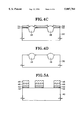
- FIGS. 5A-5E are cross-sectional views illustrating a second embodiment of the present invention as it is applied to a trench-based method.
- FIG. 5A is a cross-sectional view illustrating the step of forming active patterns which define an active region and a field region.
- the active patterns are formed by the steps of: forming a pad oxide layer 42 on semiconductor substrate 40; forming an etching blocking layer 44 on pad oxide layer 42; forming an insulating layer 46 on etching blocking layer 44; forming a photosensitive pattern 48 on insulating layer 46; and sequentially etching insulating layer 46, etching blocking layer 44, and pad oxide layer 42 by using photosensitive pattern 48 as an etching mask to thereby form an opening selectively exposing the field region of semiconductor substrate 40.
- the thermal oxide layer of, for example, of about 100 ⁇ 1,000 ⁇ thickness is used as pad oxide layer 42 and the high temperature oxide (HTO) layer of, for example, 500 ⁇ 2,000 ⁇ thickness is used as insulating layer 46.
- Etching blocking layer 44 which protects the substrate from the etchant during the photolithography used to form the trench in the semiconductor substrate, is preferably formed of one selected from the group consisting of an oxide layer, a SiN layer, SiON layer, and a double layer made of an oxide layer and a SiN layer, to a thickness of, for example, 1,000 ⁇ 2,000 ⁇ .
- FIG. 5B is a cross-sectional view illustrating the steps of forming a trench and implanting oxygen ions. These steps are sequentially performed by: selectively etching the field region of semiconductor substrate 40 to form a trench 50 and implanting oxygen ions into the bottom of the trench.
- the trench is formed to a depth of 500 ⁇ 3,500 ⁇ . It is preferred that the oxygen ions be implanted, for example, at the implantation energy of 30 ⁇ 150 KeV and with a concentration of 1.0 ⁇ 10 15 ⁇ 1.0 ⁇ 10 19 dopants/cm 2 . If necessary, the oxygen ion implantation can be carried out by multiple implantation steps of varying implantation energy and dopant concentration.
- the reference numeral 52 denotes an implanted oxygen layer.
- FIG. 5C is a cross-sectional view illustrating the step of forming a field oxide layer 54 at the bottom of trench 50. More specifically, the semiconductor substrate in which oxygen ions have been implanted is subjected to thermal oxidation to thereby form field oxide layer 54 having a thickness of about 100 ⁇ 1,000 ⁇ .
- field oxide layer 54 is formed with an upper portion above the bottom surface of the trench (i.e., filling the bottom portion of the trench) having a first thickness, and with a lower portion below the surface of the bottom of the trench having a second thickness.
- the ratio of first thickness to second thickness is 1:2. Since the upper portion of field oxide layer 54 partially fills the trench, thereby decreasing trench depth, the dishing phenomenon which may occur during succeeding planarization processes is markedly reduced.
- FIG. 5D is a cross-sectional view illustrating the steps of depositing insulation material 56 into trench 50, and planarizing the insulation material. These steps are sequentially performed by: thickly depositing insulation material 56 into trench 50 over field oxide layer 54, so as to fill the trench completely; planarizing the insulation material; and removing insulating layer (46 in FIG. 5C) .
- the planarization of insulation material 56 is performed by, for example, the CMP method using oxidation blocking layer 44 as an etch stopper.
- FIG. 5E is a cross-sectional view illustrating the step require to complete the device isolation region according to the present invention. More specifically, oxidation blocking layer (44 in FIG. 5D) and pad oxide layer (42 in FIG. 5D) are sequentially removed to thereby complete the device isolation layer which is made of field oxide layer 54 and insulation material 56 filling trench 50.
- a thicker device isolation layer as compared to the conventional trenched-based device isolation region, can be formed in the semiconductor substrate.
- Device isolation characteristics are necessarily improved.
- the dishing phenomenon which occurs during succeeding planarization, especially CMP planarization is suppressed.
- the device isolation layer of the present invention and the method for forming same in a semiconductor device, oxygen ions are implanted into a semiconductor substrate, and a field oxide layer is deeply formed into the substrate. Thus, isolation characteristics are improved and the bird's beak and/or the dishing phenomenon are suppressed.
Abstract
A method of forming a device isolation layer in a semiconductor device comprising the steps of implanting oxygen ions in a field region of a major surface of semiconductor substrate, and oxidizing the oxygen implanted region to form a field oxide layer having an upper portion of first thickness formed above the major surface of the semiconductor substrate, and a lower portion of second thickness formed in the semiconductor substrate, wherein the ratio of first thickness to second thickness is not less than 1 to 2.
Description
The present invention relates to a semiconductor device and manufacturing method for same. More particularly, the present invention relates to a device isolation layer formed in a semiconductor device, and a method for forming same this layer using oxygen ion implantation.
As semiconductor devices become ever more highly integrated, active devices formed on the semiconductor substrate have decreased to a size near or below 1 micron. This dramatic reduction in size has also taken place with respect to device isolation regions which electrically separate the active devices. The size and nature of a typical device isolation region, which is formed early in the manufacturing process of the overall semiconductor device, influence the size of the active regions subsequently formed on the semiconductor substrate, and margins between such devices. This fact requires semiconductor manufacturers to add a planarizing step to remove step differences, i.e., surface undulations, in many field insulating layers.
The conventional method of local oxidation of silicon (LOCOS) presently used by semiconductor manufacturers has several disadvantages including the "bird's beak phenomenon" caused by lateral oxidation, the formation of crystal defects in the substrate caused by heat stress, and undesired redistribution of implanted impurities used as a channel stopper. Accordingly, LOCOS fails to attain the improved electrical characteristics necessary for higher integration of semiconductor devices.
To overcome the disadvantages attendant to LOCOS, a trench isolation method has been proposed. In this method, a field oxide layer is not formed by thermal oxidation as in LOCOS. Thus, the disadvantages associated with the thermal oxidation step in LOCOS are somewhat reduced.
However, the trench isolation method is not without its own problems. For example, formation of the trench to a depth greater than the designed depth creates crystal defects in the silicon substrate. Additionally, when insulation material is filled into a broad trench, the insulation material often has an uneven profile. Such an uneven profile leads to unstable device isolation characteristics and structural step differences in the trench pattern.
The foregoing isolation methods, LOCOS and trench, will be explained in greater detail with reference to FIGS. 1A and 1B, and FIGS. 2A, 2B, 2C, and 2D.
FIGS. 1A and 1B are cross-sectional views illustrating the conventional LOCOS isolation method. Referring to FIG. 1A, a pad oxide layer 3 and a silicon nitride layer 5 are sequentially formed on a semiconductor substrate 1. A portion of silicon nitride layer 5 in a field region 9 is then removed by photolithography. Thereafter, a channel stopper ion 7 is implanted into field region 9. Thus, an active region 11 is isolated by field regions 9.
Referring now to FIG. 1B, the semiconductor substrate having field regions 9 and active region 11 is placed in an oxidation furnace and subjected to thermal oxidation under predetermined conditions to form a field oxide layers 13 from field regions 9. A channel stopper region 15 of impurities redistributed by thermal diffusion is formed under each field oxide layer 13. Also, during thermal oxidation, the semiconductor substrate adjacent to field region 9 is oxidized in a direction towards the active region 11 which leads to the bird's beak phenomenon. Thus, the "actual" field region 20 extends laterally into regions 19 to form the bird's beak, rather than remaining within the originally intended field region 17. The bird's beak phenomenon may be seen as an undesired and uncontrolled expansion of the field region beyond its intended design rule margins. This phenomenon adversely impacts attempts to maintain the fine patterns required in highly integrated semiconductor devices.
Additionally, in LOCOS, the field oxide layer is thermally grown to not less than 3,000 Å in thickness. Accordingly, the potential for crystal defect caused by the stress occurring around the boundary of the active region and the silicon nitride layer which is selectively covered on the semiconductor substrate can lead to increased leakage current between devices.
FIGS. 2A-2D are cross-sectional views sequentially illustrating the conventional trench isolation method.
Referring to FIG. 2A, a pad oxide layer 2 of about 240 Å in thickness is formed over semiconductor substrate 1 by the thermal oxidation. A silicon nitride layer 4 of about 1,500 Å thickness and a thermal oxide layer 6 of about 1,000 Å thickness are sequentially formed by low pressure chemical vapor deposition (LPCVD), and the thermal oxide layer over a field region is then removed by photolithography.
Referring to FIG. 2B, by using the thermal oxide layer remaining over the active region as an etching mask, silicon nitride 4 and pad oxide layer 2 is subjected to reactive ion etching and semiconductor substrate 1 is then dry etched to form a trench. At this time, a narrow trench region and a broad trench region coexist in the substrate in accordance with the design rule of the semiconductor device.
Thereafter, a side wall oxide layer 8 is formed inside the trench by the thermal oxidation, and polysilicon 10 is then deposited to a thickness not less than 5,000 Å, and is anisotropically etched to fill the trench with polysilicon. At this time, the narrow trench region is completely filled, but the polysilicon in the broad trench region is sunken in its center region. That is, varying loading effects occur wherein each trench depending upon the trench's size, and these loading effects determine the "filler" profile of the polysilicon.
Referring to FIG. 2C, a field oxide layer 12 is formed on the polysilicon filling the trench using a thermal oxidation process. Note that "filled" profile of the broad trench region remains sunken in its center region.
Referring to FIG. 2D, the buffer layers including the thermal oxide layer, the silicon nitride layer and the pad oxide layer, are wet etched using a buffered oxide etchant (B.O.E). The B.O.E. may comprise a mixed solution of fluoroammonium and fluorohydrogen (7:1), and phosphoric acid solution. A sacrificial oxide layer (not shown) is thereafter grown and then wet etched, whereby the formation of the device isolation process is completed.
In the trench isolation method, a gate line and bit line may be shorted, or an electrical interconnection characteristic be deteriorated by sunken center region phenomenon (indicated by the letter G in FIG. 2D) of polysilicon filling the broad trench region. At a minimum, this phenomenon reduces product yield.
The bird's beak phenomenon (indicated by the letter R in FIG. 2D) occurs during the formation of the field oxide layer and limits the reduction of the device isolation region size. Also, when the thermal oxide layer of the buffer layer is etched, the field oxide layer is simultaneously etched to a predetermined thickness. Therefore, the field oxide layer should be increased in thickness in consideration of the process margin. Accordingly, the bird's beak phenomenon is deepened, thereby precluding the desired higher integration of the semiconductor device.
In response to the foregoing problems arising in the trench isolation method, an improved trench isolation method incorporating a chemical-mechanical polishing (CMP) step has previously been proposed. This improved trench method has been considered an ideal method for completely filling the trench, and thereafter etching the insulating material over-filling the trench, because the insulation material refilled in the trench is removed in the horizontal direction. However, the added CMP step also has disadvantages such as the "dishing" phenomenon, wherein the center of the broad trench region becomes hollowed out into a dish shape when the width of the wide trench is greater than several mm. Such adverse affects create unstable device isolation characteristics and the structural step differences.
The present invention provides a LOCOS device isolation layer in a semiconductor device which allows high integration of active devices to be realized.
To achieve this result the present invention provides, in one aspect, a device isolation layer formed by LOCOS, comprising; a semiconductor substrate having a major surface, and a field oxide layer having an upper portion of first thickness formed above the major surface of the semiconductor substrate, and a lower portion of second thickness formed in the semiconductor substrate, wherein the ratio of first thickness to second thickness is not less than 1 to 2.
In another aspect, the present invention provides a device isolation layer in a semiconductor device comprising; a trench formed in a field region of a semiconductor substrate, a field oxide layer formed in a bottom portion of the trench; and an insulating layer formed over the field oxide layer to fill the trench. Additionally, the upper surface of the insulating layer may be planarized.
In yet another aspect the present invention provides a method of forming a device isolation layer in a semiconductor device comprising the steps of; implanting oxygen ions in a field region of a major surface of semiconductor substrate, and oxidizing the oxygen implanted region to form a field oxide layer having an upper portion of first thickness formed above the major surface of the semiconductor substrate, and a lower portion of second thickness formed in the semiconductor substrate, wherein the ratio of first thickness to second thickness is not less than 1 to 2.
In still another aspect, the present invention provides a method of forming a device isolation layer in a semiconductor device, comprising the steps of; forming a trench in a field region of a semiconductor substrate, implanting oxygen ions into a bottom surface of the trench, oxidizing the oxygen implanted region to form a field oxide layer which partially fills the trench, and depositing insulation material to fill the trench.
Finally, the present invention provides a method of forming a device isolation layer in a semiconductor device, comprising the steps of; forming an etch blocking layer on the surface of a semiconductor substrate, patterning the etch blocking layer to expose a portion of the semiconductor substrate, forming a trench in the exposed portion of the semiconductor substrate, implanting oxygen ions into a bottom surface of the trench, oxidizing the oxygen implanted region to form a field oxide layer having an upper portion of first thickness formed above a bottom surface of the trench to partially fill the trench, and a lower portion of second thickness formed in the semiconductor substrate below the bottom surface of the trench, wherein the ratio of first thickness to second thickness is not less than 1 to 2, depositing insulation material over field oxide layer to fill the trench, and planarizing an upper surface of the insulation material by a chemical-mechanical polishing method using the etch blocking layer and as an etch stopper.
In each of the foregoing aspects, the present invention provides a field oxide layer formed from implanted oxygen ions in a semiconductor substrate, the field oxide layer being deeply formed into the semiconductor substrate to thereby improve a device isolation characteristics, and suppress the bird's beak and or dishing phenomenon.
The foregoing advantages of the present invention will become more apparent upon consideration of the preferred embodiments set forth below with reference to the attached drawings in which:
FIGS. 1A and 1B are cross-sectional views for illustrating a conventional LOCOS isolation method;
FIGS. 2A-2D are cross-sectional views for illustrating a conventional trench isolation method;
FIG. 3 is a cross-sectional view of a device isolation layer formed according to the present invention;
FIGS. 4A-4D are cross-sectional views illustrating the formation of an isolation layer according to a first embodiment of the present invention; and,
FIGS. 5A-5E are cross-sectional views illustrating an isolation method according to a second embodiment of the present invention.
FIG. 3 is a cross-sectional view of a device isolation layer according to the present invention. In FIG. 3, the reference numeral 100 denotes a semiconductor substrate, 24 denotes a trench, 26 denotes a field oxide layer and 28 denotes an insulating layer.
As shown in FIG. 3, the device isolation layer is made of trench 24 formed in a field region of semiconductor substrate 100. Field oxide layer 26 is formed on a bottom portion of trench 24, and insulating layer 28 is then formed over field oxide layer 26 to completely fill trench 24. Preferably, insulating layer 28 will have a planar surface. Furthermore, field oxide layer 26 is preferably formed with a thickness ratio of 1:2 for an upper portion of the field oxide layer 26 formed above the plane formed by the bottom of the trench, as compared with a lower portion of the field oxide layer 26 formed below the plane of the bottom of the trench.
Accordingly, the above-described device isolation layer is more deeply formed into the semiconductor substrate when compared to the conventional device isolation layer. As such, the device isolation layer according to the present invention provides improved isolation characteristics. Additionally, as will be seen hereafter, the surface of the insulating layer may be planarized to avoid surface step differences.
FIGS. 4A-5D are cross-sectional views illustrating two preferred embodiments of the method used to form a device isolation layer according to the present invention. Specifically, FIGS. 4A-4D are cross-sectional views illustrating an isolation method according to the first embodiment of the present invention as it is applied to a LOCOS method.
Referring to FIG. 4A, the patterns for defining an active region and a field region are formed by the steps of: forming a pad oxide layer 32 and an oxidation blocking layer 34 over a semiconductor substrate 30. A photosensitive layer 36 is then formed over oxidation blocking layer 34 and patterned to remove portions of the photosensitive layer 36 overlaying the field region. Thereafter, oxidation blocking layer 34 and pad oxide layer 32 are etched by photolithography using the patterned photosensitive layer 36 as an etching mask. Thus, selected portions of the semiconductor substrate are exposed in which field regions are to be formed.
A thermal oxide layer of, for example, about 100˜1,000 Å thickness is used for pad oxide layer 32. A silicon nitride layer of, for example, about 1,000˜2,000 Å thickness is preferably used for oxidation blocking layer 34.
FIG. 4B is a cross-sectional view illustrating the oxygen ion implantation step. Oxygen ions are implanted into the exposed field regions of the semiconductor substrate, thereby forming an oxygen implanted layer 37. It is preferred that the oxygen ions are implanted at the implantation energy of 30˜150 KeV and at the dose of 1.0×10¹⁵ ˜l.0×1019 dopants/cm2. If necessary, the oxygen implantation process can be carried out using multiple implantation steps of varying implantation energy and dopant concentrations.
FIG. 4C is a cross-sectional view illustrating the step of forming a field oxide layer 38. More specifically, after removing photosensitive pattern (36 in FIG. 4B), the semiconductor substrate is subjected to thermal oxidation to form field oxide layer 38 of about 500˜3,000 Å thickness.
In this step, silicon in the substrate reacts with the implanted oxygen, as well as the oxygen provided to the substrate under conventional oxidation conditions, to form a silicon oxide layer (SiO2) The oxygen ions implanted in semiconductor substrate in the step illustrated in FIG. 4B, accelerate the oxidation process. Accordingly, the time required f or oxidation process to obtain an acceptable field oxide layer having the desired depth can b e reduced. Reduced "oxidation" time suppresses bird's beak phenomenon.
FIG. 4D is a cross-sectional view illustrating the step which completes the device isolation region. Referring to FIG. 4D, pad oxide layer 32 and oxidation blocking layer 34 are removed using conventional techniques.
Thus, according to a first embodiment of the present invention, field oxide layer 38 is deeply formed into the semiconductor substrate to thereby improve the device isolation layer characteristics. The time required to by the oxidation step to obtain an acceptable field oxide layer having a desired depth is reduced, and the bird's beak phenomenon is accordingly reduced.
FIGS. 5A-5E are cross-sectional views illustrating a second embodiment of the present invention as it is applied to a trench-based method.
FIG. 5A is a cross-sectional view illustrating the step of forming active patterns which define an active region and a field region. The active patterns are formed by the steps of: forming a pad oxide layer 42 on semiconductor substrate 40; forming an etching blocking layer 44 on pad oxide layer 42; forming an insulating layer 46 on etching blocking layer 44; forming a photosensitive pattern 48 on insulating layer 46; and sequentially etching insulating layer 46, etching blocking layer 44, and pad oxide layer 42 by using photosensitive pattern 48 as an etching mask to thereby form an opening selectively exposing the field region of semiconductor substrate 40.
It is preferred that the thermal oxide layer of, for example, of about 100˜1,000 Å thickness is used as pad oxide layer 42 and the high temperature oxide (HTO) layer of, for example, 500˜2,000 Å thickness is used as insulating layer 46. Etching blocking layer 44, which protects the substrate from the etchant during the photolithography used to form the trench in the semiconductor substrate, is preferably formed of one selected from the group consisting of an oxide layer, a SiN layer, SiON layer, and a double layer made of an oxide layer and a SiN layer, to a thickness of, for example, 1,000˜2,000 Å.
FIG. 5B is a cross-sectional view illustrating the steps of forming a trench and implanting oxygen ions. These steps are sequentially performed by: selectively etching the field region of semiconductor substrate 40 to form a trench 50 and implanting oxygen ions into the bottom of the trench.
It is preferred that the trench is formed to a depth of 500˜3,500 Å. It is preferred that the oxygen ions be implanted, for example, at the implantation energy of 30˜150 KeV and with a concentration of 1.0×10¹⁵ ˜1.0×10¹⁹ dopants/cm2. If necessary, the oxygen ion implantation can be carried out by multiple implantation steps of varying implantation energy and dopant concentration. The reference numeral 52 denotes an implanted oxygen layer.
FIG. 5C is a cross-sectional view illustrating the step of forming a field oxide layer 54 at the bottom of trench 50. More specifically, the semiconductor substrate in which oxygen ions have been implanted is subjected to thermal oxidation to thereby form field oxide layer 54 having a thickness of about 100˜1,000 Å.
During thermal oxidation, oxygen is provided from the outside the trench to further oxidize the semiconductor substrate. At this time, oxygen ions in implanted oxygen layer 52 (in FIG. 5B) formed in the bottom of trench 50 react with the silicon substrate to form field oxide layer 54. Accordingly, not only is the formation rate of field oxide layer 54 accelerated by the presence of oxygen implanted layer 52, but also field oxide layer 54 is deeply formed into the substrate. Field oxide layer 54 is formed with an upper portion above the bottom surface of the trench (i.e., filling the bottom portion of the trench) having a first thickness, and with a lower portion below the surface of the bottom of the trench having a second thickness. Preferably, the ratio of first thickness to second thickness is 1:2. Since the upper portion of field oxide layer 54 partially fills the trench, thereby decreasing trench depth, the dishing phenomenon which may occur during succeeding planarization processes is markedly reduced.
FIG. 5D is a cross-sectional view illustrating the steps of depositing insulation material 56 into trench 50, and planarizing the insulation material. These steps are sequentially performed by: thickly depositing insulation material 56 into trench 50 over field oxide layer 54, so as to fill the trench completely; planarizing the insulation material; and removing insulating layer (46 in FIG. 5C) . The planarization of insulation material 56 is performed by, for example, the CMP method using oxidation blocking layer 44 as an etch stopper.
FIG. 5E is a cross-sectional view illustrating the step require to complete the device isolation region according to the present invention. More specifically, oxidation blocking layer (44 in FIG. 5D) and pad oxide layer (42 in FIG. 5D) are sequentially removed to thereby complete the device isolation layer which is made of field oxide layer 54 and insulation material 56 filling trench 50.
According to the second embodiment of the present invention, a thicker device isolation layer, as compared to the conventional trenched-based device isolation region, can be formed in the semiconductor substrate. Device isolation characteristics are necessarily improved. As the trench depth is effectively decreased by the filling effect of the field oxide layer, the dishing phenomenon which occurs during succeeding planarization, especially CMP planarization, is suppressed.
According to the device isolation layer of the present invention and the method for forming same in a semiconductor device, oxygen ions are implanted into a semiconductor substrate, and a field oxide layer is deeply formed into the substrate. Thus, isolation characteristics are improved and the bird's beak and/or the dishing phenomenon are suppressed.
The foregoing embodiments have been given by way of example. The present invention is not limited these examples. Multiple variations and modification to the disclosed embodiments will occur to those skilled in the art upon consideration of foregoing description. Such variations and modifications, however, fall well within the scope of the present invention as set forth in the following claims.
Claims (7)
1. A method of forming a device isolation layer in a semiconductor device, comprising the steps of:
forming a trench in a field region of a semiconductor substrate;
implanting oxygen ions into a bottom surface of the trench;
oxidizing the oxygen implanted region to form a field oxide layer which partially fills the trench; and
depositing insulation material to fill the trench.
2. The method of claim 1, further comprising, prior to the step of forming the trench, the steps of:
forming an etch blocking layer over the semiconductor substrate; and
patterning the etch blocking layer to expose a portion of the semiconductor substrate in which the field region is to be formed.
3. The method of claim 2, wherein the etch blocking layer is formed of one selected from the group consisting of an oxide layer, a silicon nitride layer, a silicon oxynitride layer, and a double layer comprising an oxide layer and a silicon nitride layer.
4. The method of claim 1, wherein the step of implanting oxygen ions is performed at an implantation energy in a range of from 30 KeV to 150 KeV and at an oxygen ion dose in a range of from 1.0×10¹⁵ ions/cm2 to 1.0×10¹⁹ ions/cm2.
5. The method of claim 1, wherein the field oxide layer is formed having an upper portion of first thickness formed above a bottom surface of the trench, and a lower portion of second thickness formed in the semiconductor substrate below the bottom surface of the trench, wherein the ratio of first thickness to second thickness is not less than 1 to 2.
6. The method of claim 1, further comprising the step of planarizing an upper surface of the device isolation layer by using a chemical mechanical polishing method.
7. A method of forming a device isolation layer in a semiconductor device, comprising the steps of:
forming an etch blocking layer on the surface of a semiconductor substrate;
patterning the etch blocking layer to expose a portion of the semiconductor substrate;
forming a trench in the exposed portion of the semiconductor substrate;
implanting oxygen ions into a bottom surface of the trench;
oxidizing the oxygen implanted region to form a field oxide layer having an upper portion of first thickness formed above a bottom surface of the trench to partially fill the trench, and a lower portion of second thickness formed in the semiconductor substrate below the bottom surface of the trench, wherein the ratio of first thickness to second thickness is not less than 1 to 2;
depositing insulation material over field oxide layer to fill the trench; and,
planarizing an upper surface of the insulation material by a chemical-mechanical polishing method using the etch blocking layer and as an etch stopper.
Priority Applications (1)
| Application Number | Priority Date | Filing Date | Title |
|---|---|---|---|
| US09/022,149 US6008526A (en) | 1995-05-30 | 1998-02-11 | Device isolation layer for a semiconductor device |
Applications Claiming Priority (2)
| Application Number | Priority Date | Filing Date | Title |
|---|---|---|---|
| KR1019950013963A KR0176153B1 (en) | 1995-05-30 | 1995-05-30 | An isolation layer of a semiconductor device |
| KR199513963 | 1995-05-30 |
Related Child Applications (1)
| Application Number | Title | Priority Date | Filing Date |
|---|---|---|---|
| US09/022,149 Division US6008526A (en) | 1995-05-30 | 1998-02-11 | Device isolation layer for a semiconductor device |
Publications (1)
| Publication Number | Publication Date |
|---|---|
| US5807784A true US5807784A (en) | 1998-09-15 |
Family
ID=19415948
Family Applications (1)
| Application Number | Title | Priority Date | Filing Date |
|---|---|---|---|
| US08/567,511 Expired - Lifetime US5807784A (en) | 1995-05-30 | 1995-12-05 | Device isolation methods for a semiconductor device |
Country Status (3)
| Country | Link |
|---|---|
| US (1) | US5807784A (en) |
| JP (1) | JPH08330297A (en) |
| KR (1) | KR0176153B1 (en) |
Cited By (30)
| Publication number | Priority date | Publication date | Assignee | Title |
|---|---|---|---|---|
| US5939750A (en) * | 1998-01-21 | 1999-08-17 | Advanced Micro Devices | Use of implanted ions to reduce oxide-nitride-oxide (ONO) etch residue and polystringers |
| US5985734A (en) * | 1996-12-31 | 1999-11-16 | Hyundai Electronics Industries Co., Ltd. | Method for fabricating a semiconductor device |
| US5994200A (en) * | 1996-12-26 | 1999-11-30 | Lg Semicon Co., Ltd. | Trench isolation structure of a semiconductor device and a method for thereof |
| US5998280A (en) * | 1998-03-20 | 1999-12-07 | National Semiconductor Corporation | Modified recessed locos isolation process for deep sub-micron device processes |
| US6258693B1 (en) * | 1997-12-23 | 2001-07-10 | Integrated Device Technology, Inc. | Ion implantation for scalability of isolation in an integrated circuit |
| US6265302B1 (en) | 1999-07-12 | 2001-07-24 | Chartered Semiconductor Manufacturing Ltd. | Partially recessed shallow trench isolation method for fabricating borderless contacts |
| US6297126B1 (en) | 1999-07-12 | 2001-10-02 | Chartered Semiconductor Manufacturing Ltd. | Silicon nitride capped shallow trench isolation method for fabricating sub-micron devices with borderless contacts |
| US6399462B1 (en) * | 1997-06-30 | 2002-06-04 | Cypress Semiconductor Corporation | Method and structure for isolating integrated circuit components and/or semiconductor active devices |
| US6432797B1 (en) | 2001-01-25 | 2002-08-13 | Chartered Semiconductor Manufacturing Ltd. | Simplified method to reduce or eliminate STI oxide divots |
| US6465324B2 (en) * | 2001-03-23 | 2002-10-15 | Honeywell International Inc. | Recessed silicon oxidation for devices such as a CMOS SOI ICs |
| US6576558B1 (en) * | 2002-10-02 | 2003-06-10 | Taiwan Semiconductor Manufacturing Company | High aspect ratio shallow trench using silicon implanted oxide |
| KR20030056217A (en) * | 2001-12-27 | 2003-07-04 | 동부전자 주식회사 | shallow trench isolation forming method of semiconductor substrate |
| US6607984B1 (en) | 2000-06-20 | 2003-08-19 | International Business Machines Corporation | Removable inorganic anti-reflection coating process |
| US20040087103A1 (en) * | 2002-10-30 | 2004-05-06 | Jun Kanamori | Semiconductor device fabrication method using oxygen ion implantation |
| US20050148153A1 (en) * | 2004-01-07 | 2005-07-07 | Masahiro Takahashi | Method of dry etching semiconductor device |
| US20060134882A1 (en) * | 2004-12-22 | 2006-06-22 | Chartered Semiconductor Manufacturing Ltd. | Method to improve device isolation via fabrication of deeper shallow trench isolation regions |
| US20070029636A1 (en) * | 2005-05-30 | 2007-02-08 | Fuji Electric Device Technology Co., Ltd. | Semiconductor Device and Manufacturing Method Thereof |
| US7176104B1 (en) * | 2004-06-08 | 2007-02-13 | Integrated Device Technology, Inc. | Method for forming shallow trench isolation structure with deep oxide region |
| US20070158779A1 (en) * | 2006-01-12 | 2007-07-12 | International Business Machines Corporation | Methods and semiconductor structures for latch-up suppression using a buried damage layer |
| US20070158755A1 (en) * | 2006-01-12 | 2007-07-12 | International Business Machines Corporation | Methods and semiconductor structures for latch-up suppression using a buried conductive region |
| US20070194403A1 (en) * | 2006-02-23 | 2007-08-23 | International Business Machines Corporation | Methods for fabricating semiconductor device structures with reduced susceptibility to latch-up and semiconductor device structures formed by the methods |
| US20070241409A1 (en) * | 2006-01-26 | 2007-10-18 | International Business Machines Corporation | Semiconductor structures for latch-up suppression and methods of forming such semiconductor structures |
| US20070252731A1 (en) * | 2006-04-26 | 2007-11-01 | Magnachip Semiconductor, Ltd. | Semiconductor integrated circuit |
| CN100377332C (en) * | 2004-03-23 | 2008-03-26 | 株式会社东芝 | Semiconductor device and method of fabricating the same |
| US20080203522A1 (en) * | 2007-02-28 | 2008-08-28 | International Business Machines Corporation | Structure Incorporating Latch-Up Resistant Semiconductor Device Structures on Hybrid Substrates |
| US20080217698A1 (en) * | 2006-01-26 | 2008-09-11 | International Business Machines Corporation | Methods and semiconductor structures for latch-up suppression using a conductive region |
| US20080217690A1 (en) * | 2007-02-28 | 2008-09-11 | Jack Allan Mandelman | Latch-Up Resistant Semiconductor Structures on Hybrid Substrates and Methods for Forming Such Semiconductor Structures |
| US20090037983A1 (en) * | 2006-10-30 | 2009-02-05 | Girish Chiruvolu | User-centric authentication system and method |
| US20110081767A1 (en) * | 2007-06-05 | 2011-04-07 | Fumihiko Inoue | Precision trench formation through oxide region formation for a semiconductor device |
| CN110416089A (en) * | 2019-07-31 | 2019-11-05 | 上海华虹宏力半导体制造有限公司 | A kind of preparation method of LDMOS |
Families Citing this family (3)
| Publication number | Priority date | Publication date | Assignee | Title |
|---|---|---|---|---|
| KR100444315B1 (en) * | 1997-06-28 | 2004-11-09 | 주식회사 하이닉스반도체 | Method for manufacturing isolation layer with improved uniformity with active region of semiconductor device |
| KR100313523B1 (en) * | 1999-10-09 | 2001-11-15 | 김영환 | Manufacturing method for isolation in semiconductor device |
| US7416956B2 (en) * | 2004-11-23 | 2008-08-26 | Sandisk Corporation | Self-aligned trench filling for narrow gap isolation regions |
Citations (8)
| Publication number | Priority date | Publication date | Assignee | Title |
|---|---|---|---|---|
| JPS59188938A (en) * | 1983-04-12 | 1984-10-26 | Matsushita Electric Ind Co Ltd | Manufacture of semiconductor device |
| JPS61216456A (en) * | 1985-03-22 | 1986-09-26 | Fujitsu Ltd | Manufacture of semiconductor device |
| EP0252450A2 (en) * | 1986-07-07 | 1988-01-13 | Texas Instruments Incorporated | Integrated circuit isolation process |
| JPS63110658A (en) * | 1986-10-27 | 1988-05-16 | Nec Kansai Ltd | Manufacture of semiconductor device |
| JPH0324727A (en) * | 1989-06-22 | 1991-02-01 | Toshiba Corp | Manufacture of semiconductor device |
| US5393693A (en) * | 1994-06-06 | 1995-02-28 | United Microelectronics Corporation | "Bird-beak-less" field isolation method |
| US5445989A (en) * | 1994-08-23 | 1995-08-29 | United Microelectronics Corp. | Method of forming device isolation regions |
| US5498566A (en) * | 1993-11-15 | 1996-03-12 | Lg Semicon Co., Ltd. | Isolation region structure of semiconductor device and method for fabricating the same |
-
1995
- 1995-05-30 KR KR1019950013963A patent/KR0176153B1/en not_active IP Right Cessation
- 1995-09-21 JP JP7242594A patent/JPH08330297A/en active Pending
- 1995-12-05 US US08/567,511 patent/US5807784A/en not_active Expired - Lifetime
Patent Citations (8)
| Publication number | Priority date | Publication date | Assignee | Title |
|---|---|---|---|---|
| JPS59188938A (en) * | 1983-04-12 | 1984-10-26 | Matsushita Electric Ind Co Ltd | Manufacture of semiconductor device |
| JPS61216456A (en) * | 1985-03-22 | 1986-09-26 | Fujitsu Ltd | Manufacture of semiconductor device |
| EP0252450A2 (en) * | 1986-07-07 | 1988-01-13 | Texas Instruments Incorporated | Integrated circuit isolation process |
| JPS63110658A (en) * | 1986-10-27 | 1988-05-16 | Nec Kansai Ltd | Manufacture of semiconductor device |
| JPH0324727A (en) * | 1989-06-22 | 1991-02-01 | Toshiba Corp | Manufacture of semiconductor device |
| US5498566A (en) * | 1993-11-15 | 1996-03-12 | Lg Semicon Co., Ltd. | Isolation region structure of semiconductor device and method for fabricating the same |
| US5393693A (en) * | 1994-06-06 | 1995-02-28 | United Microelectronics Corporation | "Bird-beak-less" field isolation method |
| US5445989A (en) * | 1994-08-23 | 1995-08-29 | United Microelectronics Corp. | Method of forming device isolation regions |
Non-Patent Citations (2)
| Title |
|---|
| IBM Tech. Disc. Bull., vol. 27, No. 11, Apr. 1985, pp. 6703 6704. * |
| IBM Tech. Disc. Bull., vol. 27, No. 11, Apr. 1985, pp. 6703-6704. |
Cited By (48)
| Publication number | Priority date | Publication date | Assignee | Title |
|---|---|---|---|---|
| US5994200A (en) * | 1996-12-26 | 1999-11-30 | Lg Semicon Co., Ltd. | Trench isolation structure of a semiconductor device and a method for thereof |
| US5985734A (en) * | 1996-12-31 | 1999-11-16 | Hyundai Electronics Industries Co., Ltd. | Method for fabricating a semiconductor device |
| US6399462B1 (en) * | 1997-06-30 | 2002-06-04 | Cypress Semiconductor Corporation | Method and structure for isolating integrated circuit components and/or semiconductor active devices |
| US6258693B1 (en) * | 1997-12-23 | 2001-07-10 | Integrated Device Technology, Inc. | Ion implantation for scalability of isolation in an integrated circuit |
| US5939750A (en) * | 1998-01-21 | 1999-08-17 | Advanced Micro Devices | Use of implanted ions to reduce oxide-nitride-oxide (ONO) etch residue and polystringers |
| US5998280A (en) * | 1998-03-20 | 1999-12-07 | National Semiconductor Corporation | Modified recessed locos isolation process for deep sub-micron device processes |
| DE19911977B4 (en) * | 1998-03-20 | 2007-10-04 | National Semiconductor Corp.(N.D.Ges.D.Staates Delaware), Santa Clara | Method for introducing isolation regions into a substrate and field isolation structure in a semiconductor substrate |
| US6297126B1 (en) | 1999-07-12 | 2001-10-02 | Chartered Semiconductor Manufacturing Ltd. | Silicon nitride capped shallow trench isolation method for fabricating sub-micron devices with borderless contacts |
| US6350661B2 (en) | 1999-07-12 | 2002-02-26 | Chartered Semiconductor Manufacturing Ltd. | Silicon nitride capped shallow trench isolation method for fabricating sub-micron devices with borderless contacts |
| US6265302B1 (en) | 1999-07-12 | 2001-07-24 | Chartered Semiconductor Manufacturing Ltd. | Partially recessed shallow trench isolation method for fabricating borderless contacts |
| US6607984B1 (en) | 2000-06-20 | 2003-08-19 | International Business Machines Corporation | Removable inorganic anti-reflection coating process |
| US6432797B1 (en) | 2001-01-25 | 2002-08-13 | Chartered Semiconductor Manufacturing Ltd. | Simplified method to reduce or eliminate STI oxide divots |
| US6465324B2 (en) * | 2001-03-23 | 2002-10-15 | Honeywell International Inc. | Recessed silicon oxidation for devices such as a CMOS SOI ICs |
| KR20030056217A (en) * | 2001-12-27 | 2003-07-04 | 동부전자 주식회사 | shallow trench isolation forming method of semiconductor substrate |
| US6576558B1 (en) * | 2002-10-02 | 2003-06-10 | Taiwan Semiconductor Manufacturing Company | High aspect ratio shallow trench using silicon implanted oxide |
| US7192840B2 (en) * | 2002-10-30 | 2007-03-20 | Oki Electric Industry Co., Ltd. | Semiconductor device fabrication method using oxygen ion implantation |
| US20040087103A1 (en) * | 2002-10-30 | 2004-05-06 | Jun Kanamori | Semiconductor device fabrication method using oxygen ion implantation |
| US20050148153A1 (en) * | 2004-01-07 | 2005-07-07 | Masahiro Takahashi | Method of dry etching semiconductor device |
| US7226846B2 (en) * | 2004-01-07 | 2007-06-05 | Oki Electric Industry Co., Ltd. | Method of dry etching semiconductor substrate to reduce crystal defects in a trench |
| CN100377332C (en) * | 2004-03-23 | 2008-03-26 | 株式会社东芝 | Semiconductor device and method of fabricating the same |
| US7176104B1 (en) * | 2004-06-08 | 2007-02-13 | Integrated Device Technology, Inc. | Method for forming shallow trench isolation structure with deep oxide region |
| US20060134882A1 (en) * | 2004-12-22 | 2006-06-22 | Chartered Semiconductor Manufacturing Ltd. | Method to improve device isolation via fabrication of deeper shallow trench isolation regions |
| US20070029636A1 (en) * | 2005-05-30 | 2007-02-08 | Fuji Electric Device Technology Co., Ltd. | Semiconductor Device and Manufacturing Method Thereof |
| US7723817B2 (en) * | 2005-05-30 | 2010-05-25 | Fuji Electric Device Technology Co., Ltd. | Semiconductor device and manufacturing method thereof |
| US20070158755A1 (en) * | 2006-01-12 | 2007-07-12 | International Business Machines Corporation | Methods and semiconductor structures for latch-up suppression using a buried conductive region |
| US20070158779A1 (en) * | 2006-01-12 | 2007-07-12 | International Business Machines Corporation | Methods and semiconductor structures for latch-up suppression using a buried damage layer |
| US7648869B2 (en) | 2006-01-12 | 2010-01-19 | International Business Machines Corporation | Method of fabricating semiconductor structures for latch-up suppression |
| US7655985B2 (en) | 2006-01-26 | 2010-02-02 | International Business Machines Corporation | Methods and semiconductor structures for latch-up suppression using a conductive region |
| US7645676B2 (en) * | 2006-01-26 | 2010-01-12 | International Business Machines Corporation | Semiconductor structures for latch-up suppression and methods of forming such semiconductor structures |
| US7791145B2 (en) | 2006-01-26 | 2010-09-07 | International Business Machines Corporation | Semiconductor structures for latch-up suppression and methods of forming such semiconductor structures |
| US7727848B2 (en) | 2006-01-26 | 2010-06-01 | International Business Machines Corporation | Methods and semiconductor structures for latch-up suppression using a conductive region |
| US20080217698A1 (en) * | 2006-01-26 | 2008-09-11 | International Business Machines Corporation | Methods and semiconductor structures for latch-up suppression using a conductive region |
| US20070241409A1 (en) * | 2006-01-26 | 2007-10-18 | International Business Machines Corporation | Semiconductor structures for latch-up suppression and methods of forming such semiconductor structures |
| US20080057671A1 (en) * | 2006-01-26 | 2008-03-06 | International Business Machines Corporation | Semiconductor structures for latch-up suppression and methods of forming such semiconductor structures |
| US20080268610A1 (en) * | 2006-01-26 | 2008-10-30 | International Business Machines Corporation | Methods and semiconductor structures for latch-up suppression using a conductive region |
| US20080242016A1 (en) * | 2006-02-23 | 2008-10-02 | International Business Machines Corporation | Methods for fabricating semiconductor device structures with reduced susceptibility to latch-up and semiconductor device structures formed by the methods |
| US20070194403A1 (en) * | 2006-02-23 | 2007-08-23 | International Business Machines Corporation | Methods for fabricating semiconductor device structures with reduced susceptibility to latch-up and semiconductor device structures formed by the methods |
| US20080203492A1 (en) * | 2006-02-23 | 2008-08-28 | International Business Machines Corporation | Methods for fabricating semiconductor device structures with reduced susceptibility to latch-up and semiconductor device structures formed by the methods |
| US20070252731A1 (en) * | 2006-04-26 | 2007-11-01 | Magnachip Semiconductor, Ltd. | Semiconductor integrated circuit |
| US7884440B2 (en) * | 2006-04-26 | 2011-02-08 | Magnachip Semiconductor, Ltd. | Semiconductor integrated circuit |
| US20090037983A1 (en) * | 2006-10-30 | 2009-02-05 | Girish Chiruvolu | User-centric authentication system and method |
| US20080217690A1 (en) * | 2007-02-28 | 2008-09-11 | Jack Allan Mandelman | Latch-Up Resistant Semiconductor Structures on Hybrid Substrates and Methods for Forming Such Semiconductor Structures |
| US20080203522A1 (en) * | 2007-02-28 | 2008-08-28 | International Business Machines Corporation | Structure Incorporating Latch-Up Resistant Semiconductor Device Structures on Hybrid Substrates |
| US7754513B2 (en) | 2007-02-28 | 2010-07-13 | International Business Machines Corporation | Latch-up resistant semiconductor structures on hybrid substrates and methods for forming such semiconductor structures |
| US7818702B2 (en) | 2007-02-28 | 2010-10-19 | International Business Machines Corporation | Structure incorporating latch-up resistant semiconductor device structures on hybrid substrates |
| US20110081767A1 (en) * | 2007-06-05 | 2011-04-07 | Fumihiko Inoue | Precision trench formation through oxide region formation for a semiconductor device |
| US8354326B2 (en) * | 2007-06-05 | 2013-01-15 | Spansion Llc | Precision trench formation through oxide region formation for a semiconductor device |
| CN110416089A (en) * | 2019-07-31 | 2019-11-05 | 上海华虹宏力半导体制造有限公司 | A kind of preparation method of LDMOS |
Also Published As
| Publication number | Publication date |
|---|---|
| KR960043108A (en) | 1996-12-23 |
| KR0176153B1 (en) | 1999-04-15 |
| JPH08330297A (en) | 1996-12-13 |
Similar Documents
| Publication | Publication Date | Title |
|---|---|---|
| US5807784A (en) | Device isolation methods for a semiconductor device | |
| US5902127A (en) | Methods for forming isolation trenches including doped silicon oxide | |
| US6331469B1 (en) | Trench isolation structure, semiconductor device having the same, and trench isolation method | |
| US6187651B1 (en) | Methods of forming trench isolation regions using preferred stress relieving layers and techniques to inhibit the occurrence of voids | |
| US6174785B1 (en) | Method of forming trench isolation region for semiconductor device | |
| US5455194A (en) | Encapsulation method for localized oxidation of silicon with trench isolation | |
| US5728620A (en) | Isolation method of semiconductor device | |
| US6074927A (en) | Shallow trench isolation formation with trench wall spacer | |
| JPH09129721A (en) | Manufacture of semiconductor device | |
| US6008526A (en) | Device isolation layer for a semiconductor device | |
| US6521510B1 (en) | Method for shallow trench isolation with removal of strained island edges | |
| US5972776A (en) | Method of forming a planar isolation structure in an integrated circuit | |
| US20020003275A1 (en) | Shallow trench isolation type semiconductor device and method of the same | |
| US5371036A (en) | Locos technology with narrow silicon trench | |
| US5811346A (en) | Silicon corner rounding in shallow trench isolation process | |
| US6987064B2 (en) | Method and composition to improve a nitride/oxide wet etching selectivity | |
| US6124183A (en) | Shallow trench isolation formation with simplified reverse planarization mask | |
| US5318922A (en) | Method for manufacturing a semiconductor device | |
| US6333242B1 (en) | Method of fabricating semiconductor device without having grooves at edge portions of STI | |
| US6344374B1 (en) | Method of fabricating insulators for isolating electronic devices | |
| US6444539B1 (en) | Method for producing a shallow trench isolation filled with thermal oxide | |
| KR100221626B1 (en) | A device isolation film of semiconductor device and method for manufacturing the same | |
| KR100419754B1 (en) | A method for forming a field oxide of a semiconductor device | |
| KR100214530B1 (en) | Method for forming trench element isolation structure | |
| KR100532755B1 (en) | Method for forming shallow trench isolation |
Legal Events
| Date | Code | Title | Description |
|---|---|---|---|
| STCF | Information on status: patent grant |
Free format text: PATENTED CASE |
|
| FEPP | Fee payment procedure |
Free format text: PAYOR NUMBER ASSIGNED (ORIGINAL EVENT CODE: ASPN); ENTITY STATUS OF PATENT OWNER: LARGE ENTITY |
|
| FPAY | Fee payment |
Year of fee payment: 4 |
|
| FPAY | Fee payment |
Year of fee payment: 8 |
|
| FEPP | Fee payment procedure |
Free format text: PAYER NUMBER DE-ASSIGNED (ORIGINAL EVENT CODE: RMPN); ENTITY STATUS OF PATENT OWNER: LARGE ENTITY Free format text: PAYOR NUMBER ASSIGNED (ORIGINAL EVENT CODE: ASPN); ENTITY STATUS OF PATENT OWNER: LARGE ENTITY |
|
| FPAY | Fee payment |
Year of fee payment: 12 |