US5828428A - Resistive circuit for a thin film transistor liquid crystal display and a method for manufacturing the same - Google Patents
Resistive circuit for a thin film transistor liquid crystal display and a method for manufacturing the same Download PDFInfo
- Publication number
- US5828428A US5828428A US08/593,242 US59324296A US5828428A US 5828428 A US5828428 A US 5828428A US 59324296 A US59324296 A US 59324296A US 5828428 A US5828428 A US 5828428A
- Authority
- US
- United States
- Prior art keywords
- layer
- resistive
- amorphous silicon
- pad
- resistive circuit
- Prior art date
- Legal status (The legal status is an assumption and is not a legal conclusion. Google has not performed a legal analysis and makes no representation as to the accuracy of the status listed.)
- Expired - Lifetime
Links
- 238000000034 method Methods 0.000 title claims abstract description 25
- 239000004973 liquid crystal related substance Substances 0.000 title claims description 4
- 239000010409 thin film Substances 0.000 title claims description 4
- 238000004519 manufacturing process Methods 0.000 title description 7
- 239000002184 metal Substances 0.000 claims abstract description 32
- 229910052751 metal Inorganic materials 0.000 claims abstract description 32
- 229910021417 amorphous silicon Inorganic materials 0.000 claims abstract description 27
- 238000002161 passivation Methods 0.000 claims abstract description 22
- 238000000151 deposition Methods 0.000 claims description 11
- 238000000059 patterning Methods 0.000 claims description 9
- 239000000758 substrate Substances 0.000 claims description 8
- 238000005530 etching Methods 0.000 claims description 4
- 239000000463 material Substances 0.000 claims description 4
- 229920002120 photoresistant polymer Polymers 0.000 abstract description 5
- 229910021332 silicide Inorganic materials 0.000 abstract description 5
- FVBUAEGBCNSCDD-UHFFFAOYSA-N silicide(4-) Chemical compound [Si-4] FVBUAEGBCNSCDD-UHFFFAOYSA-N 0.000 abstract description 5
- 229910052710 silicon Inorganic materials 0.000 abstract 1
- 239000010703 silicon Substances 0.000 abstract 1
- 230000008021 deposition Effects 0.000 description 2
- 238000010586 diagram Methods 0.000 description 2
- 239000007772 electrode material Substances 0.000 description 2
- 230000015572 biosynthetic process Effects 0.000 description 1
- 238000010276 construction Methods 0.000 description 1
- 230000007423 decrease Effects 0.000 description 1
- 230000000694 effects Effects 0.000 description 1
- 239000010408 film Substances 0.000 description 1
- 238000012986 modification Methods 0.000 description 1
- 230000004048 modification Effects 0.000 description 1
- 238000006467 substitution reaction Methods 0.000 description 1
Images


Classifications
-
- G—PHYSICS
- G02—OPTICS
- G02F—OPTICAL DEVICES OR ARRANGEMENTS FOR THE CONTROL OF LIGHT BY MODIFICATION OF THE OPTICAL PROPERTIES OF THE MEDIA OF THE ELEMENTS INVOLVED THEREIN; NON-LINEAR OPTICS; FREQUENCY-CHANGING OF LIGHT; OPTICAL LOGIC ELEMENTS; OPTICAL ANALOGUE/DIGITAL CONVERTERS
- G02F1/00—Devices or arrangements for the control of the intensity, colour, phase, polarisation or direction of light arriving from an independent light source, e.g. switching, gating or modulating; Non-linear optics
- G02F1/01—Devices or arrangements for the control of the intensity, colour, phase, polarisation or direction of light arriving from an independent light source, e.g. switching, gating or modulating; Non-linear optics for the control of the intensity, phase, polarisation or colour
- G02F1/13—Devices or arrangements for the control of the intensity, colour, phase, polarisation or direction of light arriving from an independent light source, e.g. switching, gating or modulating; Non-linear optics for the control of the intensity, phase, polarisation or colour based on liquid crystals, e.g. single liquid crystal display cells
- G02F1/133—Constructional arrangements; Operation of liquid crystal cells; Circuit arrangements
- G02F1/136—Liquid crystal cells structurally associated with a semi-conducting layer or substrate, e.g. cells forming part of an integrated circuit
- G02F1/1362—Active matrix addressed cells
- G02F1/136204—Arrangements to prevent high voltage or static electricity failures
-
- G—PHYSICS
- G02—OPTICS
- G02F—OPTICAL DEVICES OR ARRANGEMENTS FOR THE CONTROL OF LIGHT BY MODIFICATION OF THE OPTICAL PROPERTIES OF THE MEDIA OF THE ELEMENTS INVOLVED THEREIN; NON-LINEAR OPTICS; FREQUENCY-CHANGING OF LIGHT; OPTICAL LOGIC ELEMENTS; OPTICAL ANALOGUE/DIGITAL CONVERTERS
- G02F1/00—Devices or arrangements for the control of the intensity, colour, phase, polarisation or direction of light arriving from an independent light source, e.g. switching, gating or modulating; Non-linear optics
- G02F1/01—Devices or arrangements for the control of the intensity, colour, phase, polarisation or direction of light arriving from an independent light source, e.g. switching, gating or modulating; Non-linear optics for the control of the intensity, phase, polarisation or colour
- G02F1/13—Devices or arrangements for the control of the intensity, colour, phase, polarisation or direction of light arriving from an independent light source, e.g. switching, gating or modulating; Non-linear optics for the control of the intensity, phase, polarisation or colour based on liquid crystals, e.g. single liquid crystal display cells
- G02F1/133—Constructional arrangements; Operation of liquid crystal cells; Circuit arrangements
- G02F1/136—Liquid crystal cells structurally associated with a semi-conducting layer or substrate, e.g. cells forming part of an integrated circuit
- G02F1/1362—Active matrix addressed cells
- G02F1/1368—Active matrix addressed cells in which the switching element is a three-electrode device
-
- H—ELECTRICITY
- H01—ELECTRIC ELEMENTS
- H01L—SEMICONDUCTOR DEVICES NOT COVERED BY CLASS H10
- H01L27/00—Devices consisting of a plurality of semiconductor or other solid-state components formed in or on a common substrate
- H01L27/02—Devices consisting of a plurality of semiconductor or other solid-state components formed in or on a common substrate including semiconductor components specially adapted for rectifying, oscillating, amplifying or switching and having at least one potential-jump barrier or surface barrier; including integrated passive circuit elements with at least one potential-jump barrier or surface barrier
- H01L27/12—Devices consisting of a plurality of semiconductor or other solid-state components formed in or on a common substrate including semiconductor components specially adapted for rectifying, oscillating, amplifying or switching and having at least one potential-jump barrier or surface barrier; including integrated passive circuit elements with at least one potential-jump barrier or surface barrier the substrate being other than a semiconductor body, e.g. an insulating body
- H01L27/1214—Devices consisting of a plurality of semiconductor or other solid-state components formed in or on a common substrate including semiconductor components specially adapted for rectifying, oscillating, amplifying or switching and having at least one potential-jump barrier or surface barrier; including integrated passive circuit elements with at least one potential-jump barrier or surface barrier the substrate being other than a semiconductor body, e.g. an insulating body comprising a plurality of TFTs formed on a non-semiconducting substrate, e.g. driving circuits for AMLCDs
- H01L27/1259—Multistep manufacturing methods
- H01L27/127—Multistep manufacturing methods with a particular formation, treatment or patterning of the active layer specially adapted to the circuit arrangement
- H01L27/1274—Multistep manufacturing methods with a particular formation, treatment or patterning of the active layer specially adapted to the circuit arrangement using crystallisation of amorphous semiconductor or recrystallisation of crystalline semiconductor
-
- H—ELECTRICITY
- H01—ELECTRIC ELEMENTS
- H01L—SEMICONDUCTOR DEVICES NOT COVERED BY CLASS H10
- H01L29/00—Semiconductor devices adapted for rectifying, amplifying, oscillating or switching, or capacitors or resistors with at least one potential-jump barrier or surface barrier, e.g. PN junction depletion layer or carrier concentration layer; Details of semiconductor bodies or of electrodes thereof ; Multistep manufacturing processes therefor
- H01L29/66—Types of semiconductor device ; Multistep manufacturing processes therefor
- H01L29/68—Types of semiconductor device ; Multistep manufacturing processes therefor controllable by only the electric current supplied, or only the electric potential applied, to an electrode which does not carry the current to be rectified, amplified or switched
- H01L29/76—Unipolar devices, e.g. field effect transistors
- H01L29/772—Field effect transistors
- H01L29/78—Field effect transistors with field effect produced by an insulated gate
- H01L29/786—Thin film transistors, i.e. transistors with a channel being at least partly a thin film
Definitions
- the present invention relates in general to a thin film transistor liquid crystal display (TFT-LCD), and more particularly, to a resistive circuit for a TFT-LCD which provides sufficient resistance to prevent electrostatic discharge, and a method for manufacturing this type of TFT-LCD.
- TFT-LCD thin film transistor liquid crystal display
- shorting bars 32, pads 31, and resistance 34 between lines 33 are necessary to test all the pixels of a conventional TFT-LCD and to prevent damage from electrostatic discharge.
- the shorting bars 32 must be cut during final processing.
- Another drawback is that the metal resistance is inadequate for large-geometry TFT-LCDs because the resistance area must be considerably large.
- the resistance 34 can be contructed by connecting two amorphous silicon TFTs 35.
- amorphous silicon has a lower electron mobility. Therefore, the size of the TFT must be increased considerably to obtain the resistance on the order of tens and hundreds of ohms which is necessary to prevent damage from electrostatic discharge, for example.
- a further object of the present invention is to provide a TFT-LCD which provides sufficient resistance to prevent damage due to eletrostatic discharge while having a reduced resistance area.
- Another object of the present invention is to provide a method for manufacturing this type of TFT-LCD.
- a TFT-LCD resistive circuit provides adequate resistance through a resistive layer formed of N + amorphous silicon and silicide.
- a first metal layer having a shorting bar and a first pad is formed over the resistive layer.
- a passivation layer is formed over the first metal layer and patterned to expose a portion of the first metal layer over the resistive layer.
- a second pad is formed on the passivation layer and connecting with the first pad. The exposed portion of the first metal layer over the resistive layer is etched down to the resistive layer, using the passivation layer as a mask. Accordingly, a conventional photoresist process is not required to form the resistive circuit
- FIG. 1 is a diagram of a resistive circuit of a prior art TFT-LCD
- FIG. 2 is a diagram showing the construction of a resistive circuit of a prior art TFT-LCD
- FIG. 3 is a cross-sectional view of a resistive circuit of another TFT-LCD
- FIGS. 4A through 4E show the fabrication process sequence of the TFT-LCD of FIG. 3;
- FIG. 5 is a cross-sectional view of a resistive circuit of a TFT-LCD of the present invention.
- FIGS. 6A through 6E show the fabrication process sequence of the TFT-LCD of FIG. 5.
- FIGS. 7A through 7E are respective cross-sectional views of FIGS. 6A through 6E.
- Resistance formed of N + amorphous silicon or silicide can be used in TFT-LCDS.
- a typical TFT-LCD having such a resistance structure is shown in FIG. 3 and the fabrication process sequence of such a typical resistance is described below with reference to FIGS. 4A through 4E.
- the process begins with the formation of a gate electrode 22 on a substrate 21 as shown in FIG. 4A.
- the amorphous silicon layer 24 and the N + amorphous silicon layer 25 are patterned at the same time. Note that this patterning process is performed at the pad.
- metal is deposited on the patterned amorphous silicon layer 24 and N + amorphous silicon layer 25 to create a source/drain electrode 26.
- the etching process is performed at the N + amorphous silicon layer 25 on which the source/drain electrode 26 is sited, as shown in FIG. 4E. This process should be performed using a photoresist film such that the N + amorphous silicon layer 25 of the resistive circuit is not etched.
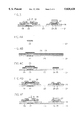
- a resistive circuit of the present invention features resistive layers including a patterned amorphous silicon layer 50 and a patterned N+ amorphous silicon layer 52 formed on a substrate 40; first metal layers including a shorting bar 41 and a first pad 42 formed on the resistive layers 50 and 52; a passivation layer 46 patterned on the first metal layers 41 and 42; and a second pad 45 patterned on the passivation layer 46 to be electrically connected with the first pad 42.
- FIGS. 6A through 6E and FIGS. 7A through 7E show what occurs on a substrate as the sequence of process steps according to the present invention is followed.
- the sequence of process steps includes successively depositing an amorphous silicon layer 50 and an N + amorphous silicon layer 52 and patterning the deposited layers to create resistive layers; depositing a metal used to create source/drain electrodes on the resistive layers 50 and 52 and patterning the metal to create first metal layers including a shorting bar 41 and a first pad 42; depositing a passivation layer 46 on the first metal layers 41 and 42 and patterning the layer to create a contact hole 53 in the first pad 42 and an aperture 54 over the resistive layers 50 and 52; depositing ITO or transparent electrode material for pixel electrode on the passivation layer 46 and patterning the material to create a second pad 45; and etching the first metal layers on the resistive layers 50 and 52 through the aperture 54 using the passivation layer 46 as a mask.
- the above-mentioned method is described below in more detail with reference to FIGS. 6A through 6E and FIGS. 7A through 7E.
- the process begins by successively depositing an amorphous silicon layer 50 and an N + amorphous silicon layer 52 on a substrate 40 and patterning the deposited layers at the same time to create resistive layers 50 and 52 as shown in FIGS. 6A and 7A.
- substrate 40 is omitted in FIGS. 6A through 6E.
- This process is followed by depositing a metal which is used for a source/drain electrode on the resistive layers 50 and 52 and patterning the deposited metal to create first metal layers including a shorting bar 41 and a pad 42, as shown in FIGS. 6B and 7B.
- a metal such as Cr, Ti and Mo is used.
- a passivation layer 46 is deposited on the first metal layers 41 and 42 and the deposited passivation layer 46 is then patterned. In this process, a contact hole 53 and an aperture 54 are patterned on the passivation layer 46.
- the deposition of metal such as ITO or transparent electrode material used for a pixel electrode is conducted on the passivation layer 46 and patterned the deposited metal to create a second pad 45.
- the etching process is performed at the first metal layers 41 and 42 under which the resistive layers are sited using the passivation layer 46 as mask.
- the size of the resistive area can be reduced while still providing adequate resistance for the production of TFT-LCDs by virtue of the N + amorphous silicon and silicide.
- the TFT-LCD can be fabricated without requiring any additional photoresist process.
- this TFT-LCD can provide sufficient resistance, in the range of tens to hundreds of ohms for example, to prevent damage due to electrostatic discharge.
Abstract
Description
Claims (8)
Applications Claiming Priority (2)
| Application Number | Priority Date | Filing Date | Title |
|---|---|---|---|
| KR1019950001529A KR0145902B1 (en) | 1995-01-27 | 1995-01-27 | Resistance part and its manufacturing method of thin film transistor liquid crystal display elements |
| KR1995-1529 | 1995-01-27 |
Publications (1)
| Publication Number | Publication Date |
|---|---|
| US5828428A true US5828428A (en) | 1998-10-27 |
Family
ID=19407377
Family Applications (1)
| Application Number | Title | Priority Date | Filing Date |
|---|---|---|---|
| US08/593,242 Expired - Lifetime US5828428A (en) | 1995-01-27 | 1996-01-29 | Resistive circuit for a thin film transistor liquid crystal display and a method for manufacturing the same |
Country Status (2)
| Country | Link |
|---|---|
| US (1) | US5828428A (en) |
| KR (1) | KR0145902B1 (en) |
Cited By (18)
| Publication number | Priority date | Publication date | Assignee | Title |
|---|---|---|---|---|
| US6072550A (en) * | 1996-06-11 | 2000-06-06 | Samsung Electronics Co., Ltd. | Liquid crystal display having resistive electrostatic discharge protection devices with resistance no greater than 1 MOHM and method of fabrication |
| US6088073A (en) * | 1997-04-14 | 2000-07-11 | Casio Computer Co., Ltd. | Display device with destaticizing elements and an electrostatic pulse delaying element connected to each of the destaticizing elements |
| US6100949A (en) * | 1996-11-29 | 2000-08-08 | Lg Electronics Inc. | Liquid crystal display device having electrostatic discharge protection |
| US6128051A (en) * | 1997-09-12 | 2000-10-03 | Lg Electronics Inc. | Method for forming and apparatus including a liquid crystal display having shorting bar connector |
| US6310666B1 (en) * | 1997-10-24 | 2001-10-30 | Lg. Philips Lcd Co., Ltd. | Manufacturing method of liquid crystal display preventing RF discharge damage |
| US20030117537A1 (en) * | 1997-03-26 | 2003-06-26 | Sharp Kabushiki Kaisha | Display panel |
| US20030151568A1 (en) * | 1997-07-02 | 2003-08-14 | Seiko Epson Corporation | Display apparatus |
| US20040028588A1 (en) * | 2001-08-06 | 2004-02-12 | Webb Cynthia C. | Method for accelerated aging of catalytic converters incorporating injection of volatilized lubricant |
| WO2004063799A1 (en) * | 2002-12-03 | 2004-07-29 | Quanta Display Inc. | Method for manufacturing the thin film transistor array |
| US20080036699A1 (en) * | 1997-08-21 | 2008-02-14 | Seiko Epson Corporation | Active matrix display device |
| US20080180421A1 (en) * | 1997-08-21 | 2008-07-31 | Seiko Epson Corporation | Active matrix display device |
| US20080192162A1 (en) * | 2007-02-08 | 2008-08-14 | Toshiba Matsushita Display Technology Co., Ltd. | Liquid crystal display device |
| US20090079464A1 (en) * | 2007-09-25 | 2009-03-26 | Seiko Epson Corporation | Electro-optical device and electronic apparatus |
| US20110121095A1 (en) * | 2008-06-11 | 2011-05-26 | Daniel Crichton | Fluid feed system improvements |
| US20110168804A1 (en) * | 2008-06-11 | 2011-07-14 | Daniel Crichton | Fluid feed system improvements |
| US8411217B2 (en) * | 2007-07-12 | 2013-04-02 | Chunghwa Picture Tubes, Ltd. | Active device array substrate with protecting electrostatic discharge circuit having switching devices |
| CN104778909A (en) * | 2014-01-15 | 2015-07-15 | 三星显示有限公司 | Display panel and display device including the same |
| CN107316838A (en) * | 2017-06-30 | 2017-11-03 | 上海中航光电子有限公司 | Array base palte, preparation method, touch-control display panel and touch control display apparatus |
Citations (5)
| Publication number | Priority date | Publication date | Assignee | Title |
|---|---|---|---|---|
| US4789857A (en) * | 1986-01-27 | 1988-12-06 | Francois Maurice | Active matrix display screen with line and column redundancy |
| US5019001A (en) * | 1988-12-21 | 1991-05-28 | Kabushiki Kaisha Toshiba | Method for manufacturing liquid crystal display device |
| US5068748A (en) * | 1989-10-20 | 1991-11-26 | Hosiden Corporation | Active matrix liquid crystal display device having improved electrostatic discharge protection |
| US5187604A (en) * | 1989-01-18 | 1993-02-16 | Hitachi, Ltd. | Multi-layer external terminals of liquid crystal displays with thin-film transistors |
| US5650834A (en) * | 1994-07-05 | 1997-07-22 | Mitsubishi Denki Kabushiki Kaisha | Active-matrix device having silicide thin film resistor disposed between an input terminal and a short-circuit ring |
-
1995
- 1995-01-27 KR KR1019950001529A patent/KR0145902B1/en not_active IP Right Cessation
-
1996
- 1996-01-29 US US08/593,242 patent/US5828428A/en not_active Expired - Lifetime
Patent Citations (5)
| Publication number | Priority date | Publication date | Assignee | Title |
|---|---|---|---|---|
| US4789857A (en) * | 1986-01-27 | 1988-12-06 | Francois Maurice | Active matrix display screen with line and column redundancy |
| US5019001A (en) * | 1988-12-21 | 1991-05-28 | Kabushiki Kaisha Toshiba | Method for manufacturing liquid crystal display device |
| US5187604A (en) * | 1989-01-18 | 1993-02-16 | Hitachi, Ltd. | Multi-layer external terminals of liquid crystal displays with thin-film transistors |
| US5068748A (en) * | 1989-10-20 | 1991-11-26 | Hosiden Corporation | Active matrix liquid crystal display device having improved electrostatic discharge protection |
| US5650834A (en) * | 1994-07-05 | 1997-07-22 | Mitsubishi Denki Kabushiki Kaisha | Active-matrix device having silicide thin film resistor disposed between an input terminal and a short-circuit ring |
Cited By (37)
| Publication number | Priority date | Publication date | Assignee | Title |
|---|---|---|---|---|
| US6072550A (en) * | 1996-06-11 | 2000-06-06 | Samsung Electronics Co., Ltd. | Liquid crystal display having resistive electrostatic discharge protection devices with resistance no greater than 1 MOHM and method of fabrication |
| US6100949A (en) * | 1996-11-29 | 2000-08-08 | Lg Electronics Inc. | Liquid crystal display device having electrostatic discharge protection |
| US20030117537A1 (en) * | 1997-03-26 | 2003-06-26 | Sharp Kabushiki Kaisha | Display panel |
| US6088073A (en) * | 1997-04-14 | 2000-07-11 | Casio Computer Co., Ltd. | Display device with destaticizing elements and an electrostatic pulse delaying element connected to each of the destaticizing elements |
| US8803773B2 (en) | 1997-07-02 | 2014-08-12 | Intellectual Keystone Technology Llc | Display apparatus |
| US20030151568A1 (en) * | 1997-07-02 | 2003-08-14 | Seiko Epson Corporation | Display apparatus |
| US8310475B2 (en) | 1997-07-02 | 2012-11-13 | Seiko Epson Corporation | Display apparatus |
| US20080165174A1 (en) * | 1997-07-02 | 2008-07-10 | Seiko Epson Corporation | Display apparatus |
| US20080198152A1 (en) * | 1997-07-02 | 2008-08-21 | Seiko Epson Corporation | Display apparatus |
| US8334858B2 (en) | 1997-07-02 | 2012-12-18 | Seiko Epson Corporation | Display apparatus |
| US8310476B2 (en) | 1997-07-02 | 2012-11-13 | Seiko Epson Corporation | Display apparatus |
| US8159124B2 (en) | 1997-08-21 | 2012-04-17 | Seiko Epson Corporation | Active matrix display device |
| US20080036699A1 (en) * | 1997-08-21 | 2008-02-14 | Seiko Epson Corporation | Active matrix display device |
| US20080180421A1 (en) * | 1997-08-21 | 2008-07-31 | Seiko Epson Corporation | Active matrix display device |
| US20090303165A1 (en) * | 1997-08-21 | 2009-12-10 | Seiko Epson Corporation | Active matrix display device |
| US6128051A (en) * | 1997-09-12 | 2000-10-03 | Lg Electronics Inc. | Method for forming and apparatus including a liquid crystal display having shorting bar connector |
| US6310666B1 (en) * | 1997-10-24 | 2001-10-30 | Lg. Philips Lcd Co., Ltd. | Manufacturing method of liquid crystal display preventing RF discharge damage |
| US20040028588A1 (en) * | 2001-08-06 | 2004-02-12 | Webb Cynthia C. | Method for accelerated aging of catalytic converters incorporating injection of volatilized lubricant |
| WO2004063799A1 (en) * | 2002-12-03 | 2004-07-29 | Quanta Display Inc. | Method for manufacturing the thin film transistor array |
| US7796203B2 (en) * | 2007-02-08 | 2010-09-14 | Toshiba Matsushita Display Technology Co., Ltd. | Liquid crystal display device |
| US20080192162A1 (en) * | 2007-02-08 | 2008-08-14 | Toshiba Matsushita Display Technology Co., Ltd. | Liquid crystal display device |
| US8411217B2 (en) * | 2007-07-12 | 2013-04-02 | Chunghwa Picture Tubes, Ltd. | Active device array substrate with protecting electrostatic discharge circuit having switching devices |
| TWI400785B (en) * | 2007-07-12 | 2013-07-01 | Chunghwa Picture Tubes Ltd | Active devices array substrate |
| US20090079464A1 (en) * | 2007-09-25 | 2009-03-26 | Seiko Epson Corporation | Electro-optical device and electronic apparatus |
| US7750662B2 (en) | 2007-09-25 | 2010-07-06 | Seiko Epson Corporation | Electro-optical device and electronic apparatus |
| EP2043084A1 (en) * | 2007-09-25 | 2009-04-01 | Seiko Epson Corporation | Electro-optical device and electronic apparatus |
| CN101398544B (en) * | 2007-09-25 | 2013-04-10 | 精工爱普生株式会社 | Electro-optical device and electronic apparatus |
| US8840039B2 (en) * | 2008-06-11 | 2014-09-23 | The Technology Partnership Plc | Fluid feed system improvements |
| US20110121095A1 (en) * | 2008-06-11 | 2011-05-26 | Daniel Crichton | Fluid feed system improvements |
| US8840040B2 (en) * | 2008-06-11 | 2014-09-23 | The Technology Partnership Plc | Fluid feed system improvements |
| US20110168804A1 (en) * | 2008-06-11 | 2011-07-14 | Daniel Crichton | Fluid feed system improvements |
| CN104778909A (en) * | 2014-01-15 | 2015-07-15 | 三星显示有限公司 | Display panel and display device including the same |
| US20150199929A1 (en) * | 2014-01-15 | 2015-07-16 | Samsung Display Co., Ltd. | Display panel and display device including the same |
| US9691314B2 (en) * | 2014-01-15 | 2017-06-27 | Samsung Display Co., Ltd | Display panel and display device including the same |
| CN107316838A (en) * | 2017-06-30 | 2017-11-03 | 上海中航光电子有限公司 | Array base palte, preparation method, touch-control display panel and touch control display apparatus |
| US10324554B2 (en) * | 2017-06-30 | 2019-06-18 | Shanghai Avic Opto Electronics Co., Ltd. | Array substrate and manufacturing method thereof, touch display panel and touch display apparatus |
| CN107316838B (en) * | 2017-06-30 | 2020-03-10 | 上海中航光电子有限公司 | Array substrate, manufacturing method, touch display panel and touch display device |
Also Published As
| Publication number | Publication date |
|---|---|
| KR960029866A (en) | 1996-08-17 |
| KR0145902B1 (en) | 1998-09-15 |
Similar Documents
| Publication | Publication Date | Title |
|---|---|---|
| US6768521B2 (en) | Method for manufacturing a thin film transistor array panel | |
| US5828428A (en) | Resistive circuit for a thin film transistor liquid crystal display and a method for manufacturing the same | |
| US6927105B2 (en) | Thin film transistor array substrate and manufacturing method thereof | |
| US5828433A (en) | Liquid crystal display device and a method of manufacturing the same | |
| US6338989B1 (en) | Array substrate for use in liquid crystal display device and method of manufacturing the same | |
| US6448579B1 (en) | Thin film transistor array substrate for liquid crystal display and a method for fabricating the same | |
| US8289463B2 (en) | Manufacturing method for a thin film transistor-liquid crystal display having an insulating layer exposing portions of a gate island | |
| US7435629B2 (en) | Thin film transistor array panel and a manufacturing method thereof | |
| US5998230A (en) | Method for making liquid crystal display device with reduced mask steps | |
| US20070102770A1 (en) | Thin film transistor array panel and manufacturing method thereof | |
| US20080299712A1 (en) | Manufacturing method of a thin film transistor array panel | |
| US6654074B1 (en) | Array substrate for liquid crystal display device with shorting bars external to a data pad and method of manufacturing the same | |
| US7005331B2 (en) | Method of manufacturing a thin film transistor array | |
| JPH11133455A (en) | Production of liquid crystal display device | |
| US5995174A (en) | Liquid crystal display apparatus with source/drain electrodes and pixel electrode formed by the same material | |
| US6043000A (en) | Method for manufacturing a semiconductor device | |
| US20050041187A1 (en) | Thin film transistor array panel for liquid crystal display and method for manufacturing the same | |
| US6746959B2 (en) | Liquid crystal display and method | |
| US6870187B2 (en) | Thin film transistor array panel and manufacturing method thereof | |
| US20040207791A1 (en) | Method of manufacturing IPS-LCD using 4-mask process | |
| US6940095B2 (en) | Method of fabricating thin film transistor array | |
| KR100897720B1 (en) | Fabrication method of Liquid Crystal Display | |
| JP2002314088A (en) | Manufacturing method for thin film transistor array substrate and liquid crystal display device using the same manufactured by the method | |
| US7060540B2 (en) | Method of fabricating thin film transistor array | |
| US20020085135A1 (en) | Liquid crystal display device and fabricating method thereof |
Legal Events
| Date | Code | Title | Description |
|---|---|---|---|
| AS | Assignment |
Owner name: SAMSUNG ELECTRONICS CO., LTD., KOREA, REPUBLIC OF Free format text: ASSIGNMENT OF ASSIGNORS INTEREST;ASSIGNORS:KIM, DONG-GYU;PARK, WOON-YONG;REEL/FRAME:007944/0804 Effective date: 19960305 |
|
| STCF | Information on status: patent grant |
Free format text: PATENTED CASE |
|
| FEPP | Fee payment procedure |
Free format text: PAYOR NUMBER ASSIGNED (ORIGINAL EVENT CODE: ASPN); ENTITY STATUS OF PATENT OWNER: LARGE ENTITY |
|
| FPAY | Fee payment |
Year of fee payment: 4 |
|
| FPAY | Fee payment |
Year of fee payment: 8 |
|
| FPAY | Fee payment |
Year of fee payment: 12 |
|
| AS | Assignment |
Owner name: SAMSUNG DISPLAY CO., LTD., KOREA, REPUBLIC OF Free format text: ASSIGNMENT OF ASSIGNORS INTEREST;ASSIGNOR:SAMSUNG ELECTRONICS CO., LTD.;REEL/FRAME:028984/0774 Effective date: 20120904 |