US5834817A - Field effect transistor with a shaped gate electrode - Google Patents
Field effect transistor with a shaped gate electrode Download PDFInfo
- Publication number
- US5834817A US5834817A US07/983,931 US98393192A US5834817A US 5834817 A US5834817 A US 5834817A US 98393192 A US98393192 A US 98393192A US 5834817 A US5834817 A US 5834817A
- Authority
- US
- United States
- Prior art keywords
- impurity
- main surface
- conductive layer
- layer
- shaped conductive
- Prior art date
- Legal status (The legal status is an assumption and is not a legal conclusion. Google has not performed a legal analysis and makes no representation as to the accuracy of the status listed.)
- Expired - Fee Related
Links
- 230000005669 field effect Effects 0.000 title claims abstract description 11
- 239000012535 impurity Substances 0.000 claims abstract description 64
- 239000000758 substrate Substances 0.000 claims abstract description 48
- 239000004065 semiconductor Substances 0.000 claims abstract description 33
- 238000005530 etching Methods 0.000 claims description 37
- 229910021420 polycrystalline silicon Inorganic materials 0.000 claims description 21
- 229920005591 polysilicon Polymers 0.000 claims description 20
- 239000000463 material Substances 0.000 claims description 3
- 239000000203 mixture Substances 0.000 abstract description 7
- 239000010410 layer Substances 0.000 description 132
- 238000000034 method Methods 0.000 description 27
- VYPSYNLAJGMNEJ-UHFFFAOYSA-N Silicium dioxide Chemical compound O=[Si]=O VYPSYNLAJGMNEJ-UHFFFAOYSA-N 0.000 description 24
- 238000004519 manufacturing process Methods 0.000 description 24
- 150000002500 ions Chemical class 0.000 description 12
- 239000002784 hot electron Substances 0.000 description 10
- 229910052814 silicon oxide Inorganic materials 0.000 description 10
- 230000000694 effects Effects 0.000 description 9
- 230000005684 electric field Effects 0.000 description 8
- 238000010438 heat treatment Methods 0.000 description 7
- 235000012239 silicon dioxide Nutrition 0.000 description 7
- 239000000377 silicon dioxide Substances 0.000 description 7
- 230000015572 biosynthetic process Effects 0.000 description 6
- 239000013078 crystal Substances 0.000 description 5
- 230000007547 defect Effects 0.000 description 5
- 238000009792 diffusion process Methods 0.000 description 5
- -1 phosphorous ion Chemical class 0.000 description 4
- 238000001020 plasma etching Methods 0.000 description 4
- 230000015556 catabolic process Effects 0.000 description 3
- 238000006731 degradation reaction Methods 0.000 description 3
- 238000010586 diagram Methods 0.000 description 3
- 239000007789 gas Substances 0.000 description 3
- 230000008018 melting Effects 0.000 description 3
- 238000002844 melting Methods 0.000 description 3
- 229910052751 metal Inorganic materials 0.000 description 3
- 239000002184 metal Substances 0.000 description 3
- XUIMIQQOPSSXEZ-UHFFFAOYSA-N Silicon Chemical compound [Si] XUIMIQQOPSSXEZ-UHFFFAOYSA-N 0.000 description 2
- 239000000969 carrier Substances 0.000 description 2
- 238000005229 chemical vapour deposition Methods 0.000 description 2
- 239000004020 conductor Substances 0.000 description 2
- 230000008878 coupling Effects 0.000 description 2
- 238000010168 coupling process Methods 0.000 description 2
- 238000005859 coupling reaction Methods 0.000 description 2
- 239000012495 reaction gas Substances 0.000 description 2
- 229910052710 silicon Inorganic materials 0.000 description 2
- 239000010703 silicon Substances 0.000 description 2
- 238000000992 sputter etching Methods 0.000 description 2
- 239000000126 substance Substances 0.000 description 2
- TXEYQDLBPFQVAA-UHFFFAOYSA-N tetrafluoromethane Chemical compound FC(F)(F)F TXEYQDLBPFQVAA-UHFFFAOYSA-N 0.000 description 2
- HAYXDMNJJFVXCI-UHFFFAOYSA-N arsenic(5+) Chemical compound [As+5] HAYXDMNJJFVXCI-UHFFFAOYSA-N 0.000 description 1
- QVGXLLKOCUKJST-UHFFFAOYSA-N atomic oxygen Chemical compound [O] QVGXLLKOCUKJST-UHFFFAOYSA-N 0.000 description 1
- 150000001875 compounds Chemical class 0.000 description 1
- 238000007796 conventional method Methods 0.000 description 1
- 239000011737 fluorine Substances 0.000 description 1
- 229910052731 fluorine Inorganic materials 0.000 description 1
- 239000007943 implant Substances 0.000 description 1
- 238000002513 implantation Methods 0.000 description 1
- 238000005468 ion implantation Methods 0.000 description 1
- GALOTNBSUVEISR-UHFFFAOYSA-N molybdenum;silicon Chemical compound [Mo]#[Si] GALOTNBSUVEISR-UHFFFAOYSA-N 0.000 description 1
- 230000007935 neutral effect Effects 0.000 description 1
- 229920000620 organic polymer Polymers 0.000 description 1
- 229910052760 oxygen Inorganic materials 0.000 description 1
- 239000001301 oxygen Substances 0.000 description 1
- 239000002356 single layer Substances 0.000 description 1
- 239000007787 solid Substances 0.000 description 1
- 239000013589 supplement Substances 0.000 description 1
Images


Classifications
-
- H—ELECTRICITY
- H01—ELECTRIC ELEMENTS
- H01L—SEMICONDUCTOR DEVICES NOT COVERED BY CLASS H10
- H01L29/00—Semiconductor devices adapted for rectifying, amplifying, oscillating or switching, or capacitors or resistors with at least one potential-jump barrier or surface barrier, e.g. PN junction depletion layer or carrier concentration layer; Details of semiconductor bodies or of electrodes thereof ; Multistep manufacturing processes therefor
- H01L29/66—Types of semiconductor device ; Multistep manufacturing processes therefor
- H01L29/66007—Multistep manufacturing processes
- H01L29/66075—Multistep manufacturing processes of devices having semiconductor bodies comprising group 14 or group 13/15 materials
- H01L29/66227—Multistep manufacturing processes of devices having semiconductor bodies comprising group 14 or group 13/15 materials the devices being controllable only by the electric current supplied or the electric potential applied, to an electrode which does not carry the current to be rectified, amplified or switched, e.g. three-terminal devices
- H01L29/66409—Unipolar field-effect transistors
- H01L29/66477—Unipolar field-effect transistors with an insulated gate, i.e. MISFET
- H01L29/66568—Lateral single gate silicon transistors
- H01L29/66575—Lateral single gate silicon transistors where the source and drain or source and drain extensions are self-aligned to the sides of the gate
- H01L29/6659—Lateral single gate silicon transistors where the source and drain or source and drain extensions are self-aligned to the sides of the gate with both lightly doped source and drain extensions and source and drain self-aligned to the sides of the gate, e.g. lightly doped drain [LDD] MOSFET, double diffused drain [DDD] MOSFET
- H01L29/66598—Lateral single gate silicon transistors where the source and drain or source and drain extensions are self-aligned to the sides of the gate with both lightly doped source and drain extensions and source and drain self-aligned to the sides of the gate, e.g. lightly doped drain [LDD] MOSFET, double diffused drain [DDD] MOSFET forming drain [D] and lightly doped drain [LDD] simultaneously, e.g. using implantation through the wings a T-shaped layer, or through a specially shaped layer
-
- H—ELECTRICITY
- H01—ELECTRIC ELEMENTS
- H01L—SEMICONDUCTOR DEVICES NOT COVERED BY CLASS H10
- H01L21/00—Processes or apparatus adapted for the manufacture or treatment of semiconductor or solid state devices or of parts thereof
- H01L21/02—Manufacture or treatment of semiconductor devices or of parts thereof
- H01L21/04—Manufacture or treatment of semiconductor devices or of parts thereof the devices having at least one potential-jump barrier or surface barrier, e.g. PN junction, depletion layer or carrier concentration layer
- H01L21/18—Manufacture or treatment of semiconductor devices or of parts thereof the devices having at least one potential-jump barrier or surface barrier, e.g. PN junction, depletion layer or carrier concentration layer the devices having semiconductor bodies comprising elements of Group IV of the Periodic System or AIIIBV compounds with or without impurities, e.g. doping materials
- H01L21/28—Manufacture of electrodes on semiconductor bodies using processes or apparatus not provided for in groups H01L21/20 - H01L21/268
- H01L21/28008—Making conductor-insulator-semiconductor electrodes
- H01L21/28017—Making conductor-insulator-semiconductor electrodes the insulator being formed after the semiconductor body, the semiconductor being silicon
- H01L21/28026—Making conductor-insulator-semiconductor electrodes the insulator being formed after the semiconductor body, the semiconductor being silicon characterised by the conductor
- H01L21/28035—Making conductor-insulator-semiconductor electrodes the insulator being formed after the semiconductor body, the semiconductor being silicon characterised by the conductor the final conductor layer next to the insulator being silicon, e.g. polysilicon, with or without impurities
- H01L21/28044—Making conductor-insulator-semiconductor electrodes the insulator being formed after the semiconductor body, the semiconductor being silicon characterised by the conductor the final conductor layer next to the insulator being silicon, e.g. polysilicon, with or without impurities the conductor comprising at least another non-silicon conductive layer
- H01L21/28061—Making conductor-insulator-semiconductor electrodes the insulator being formed after the semiconductor body, the semiconductor being silicon characterised by the conductor the final conductor layer next to the insulator being silicon, e.g. polysilicon, with or without impurities the conductor comprising at least another non-silicon conductive layer the conductor comprising a metal or metal silicide formed by deposition, e.g. sputter deposition, i.e. without a silicidation reaction
-
- H—ELECTRICITY
- H01—ELECTRIC ELEMENTS
- H01L—SEMICONDUCTOR DEVICES NOT COVERED BY CLASS H10
- H01L21/00—Processes or apparatus adapted for the manufacture or treatment of semiconductor or solid state devices or of parts thereof
- H01L21/02—Manufacture or treatment of semiconductor devices or of parts thereof
- H01L21/04—Manufacture or treatment of semiconductor devices or of parts thereof the devices having at least one potential-jump barrier or surface barrier, e.g. PN junction, depletion layer or carrier concentration layer
- H01L21/18—Manufacture or treatment of semiconductor devices or of parts thereof the devices having at least one potential-jump barrier or surface barrier, e.g. PN junction, depletion layer or carrier concentration layer the devices having semiconductor bodies comprising elements of Group IV of the Periodic System or AIIIBV compounds with or without impurities, e.g. doping materials
- H01L21/28—Manufacture of electrodes on semiconductor bodies using processes or apparatus not provided for in groups H01L21/20 - H01L21/268
- H01L21/28008—Making conductor-insulator-semiconductor electrodes
- H01L21/28017—Making conductor-insulator-semiconductor electrodes the insulator being formed after the semiconductor body, the semiconductor being silicon
- H01L21/28026—Making conductor-insulator-semiconductor electrodes the insulator being formed after the semiconductor body, the semiconductor being silicon characterised by the conductor
- H01L21/28114—Making conductor-insulator-semiconductor electrodes the insulator being formed after the semiconductor body, the semiconductor being silicon characterised by the conductor characterised by the sectional shape, e.g. T, inverted-T
-
- H—ELECTRICITY
- H01—ELECTRIC ELEMENTS
- H01L—SEMICONDUCTOR DEVICES NOT COVERED BY CLASS H10
- H01L29/00—Semiconductor devices adapted for rectifying, amplifying, oscillating or switching, or capacitors or resistors with at least one potential-jump barrier or surface barrier, e.g. PN junction depletion layer or carrier concentration layer; Details of semiconductor bodies or of electrodes thereof ; Multistep manufacturing processes therefor
- H01L29/40—Electrodes ; Multistep manufacturing processes therefor
- H01L29/41—Electrodes ; Multistep manufacturing processes therefor characterised by their shape, relative sizes or dispositions
- H01L29/423—Electrodes ; Multistep manufacturing processes therefor characterised by their shape, relative sizes or dispositions not carrying the current to be rectified, amplified or switched
- H01L29/42312—Gate electrodes for field effect devices
- H01L29/42316—Gate electrodes for field effect devices for field-effect transistors
- H01L29/4232—Gate electrodes for field effect devices for field-effect transistors with insulated gate
- H01L29/42372—Gate electrodes for field effect devices for field-effect transistors with insulated gate characterised by the conducting layer, e.g. the length, the sectional shape or the lay-out
- H01L29/42376—Gate electrodes for field effect devices for field-effect transistors with insulated gate characterised by the conducting layer, e.g. the length, the sectional shape or the lay-out characterised by the length or the sectional shape
-
- H—ELECTRICITY
- H01—ELECTRIC ELEMENTS
- H01L—SEMICONDUCTOR DEVICES NOT COVERED BY CLASS H10
- H01L29/00—Semiconductor devices adapted for rectifying, amplifying, oscillating or switching, or capacitors or resistors with at least one potential-jump barrier or surface barrier, e.g. PN junction depletion layer or carrier concentration layer; Details of semiconductor bodies or of electrodes thereof ; Multistep manufacturing processes therefor
- H01L29/66—Types of semiconductor device ; Multistep manufacturing processes therefor
- H01L29/66007—Multistep manufacturing processes
- H01L29/66075—Multistep manufacturing processes of devices having semiconductor bodies comprising group 14 or group 13/15 materials
- H01L29/66227—Multistep manufacturing processes of devices having semiconductor bodies comprising group 14 or group 13/15 materials the devices being controllable only by the electric current supplied or the electric potential applied, to an electrode which does not carry the current to be rectified, amplified or switched, e.g. three-terminal devices
- H01L29/66409—Unipolar field-effect transistors
- H01L29/66477—Unipolar field-effect transistors with an insulated gate, i.e. MISFET
- H01L29/66568—Lateral single gate silicon transistors
- H01L29/66575—Lateral single gate silicon transistors where the source and drain or source and drain extensions are self-aligned to the sides of the gate
- H01L29/6659—Lateral single gate silicon transistors where the source and drain or source and drain extensions are self-aligned to the sides of the gate with both lightly doped source and drain extensions and source and drain self-aligned to the sides of the gate, e.g. lightly doped drain [LDD] MOSFET, double diffused drain [DDD] MOSFET
Definitions
- the present invention relates generally to a field effect transistor and, more particularly, to a field effect transistor capable of high speed operation, and to manufacturing methods therefor.
- FIGS. 1A to 1D show a conventional manufacturing process for a conventional FET in a stepwise manner.
- a silicon oxide film 2a is formed on a P type semiconductor substrate.
- a layer 3a of silicon or a conductive material such as a metal having a high melting point is formed on the silicon oxide film.
- FIG. 1A The polysilicon layer 3a and the silicon oxide film 2 are simultaneously etched by a known etching method, and a gate electrode 3 and a gate insulating film 2 are formed (FIG. 1B).
- a known etching method is disclosed in, for example, "Microfabrication Technique by Gas Plasma Etching Method," H. Komiya et al, Proc.
- N type impurities are implanted from above the semiconductor substrate 1 using the gate electrode 3 as a mask. Thereafter, a heat treatment is performed. Consequently, N + impurity layers 4a and 4b are formed on a main surface of the semiconductor substrate 1 in self alignment.
- the N + impurity layers 4a and 4b constitute a source and a drain of a transistor (FIG. 1C).
- An Al wiring layer is formed connected to the N + impurity layers (FIG. 1D).
- FIG. 2A An enlarged view of the gate portion of the FET transistor structure as described above is shown in FIG. 2A.
- the overlapping portion ( ⁇ L) constitutes an additional capacitance between the gate and the source ⁇ drain as shown in the equivalent circuit of FIG. 2B. Therefore, if this MOS transistor is used in an integrated circuit or the like, the MOS transistor cannot operate at a high speed and the power consumption of the MOS transistor is relatively large. If the dimension of the overlapping portion is relatively large, a so-called short channel effect will occur, thereby causing problems such as a change in the threshold voltage of the MOS transistor. Therefore, the overlapping portion is also an obstruction in reducing the size of the MOS transistor.
- FIG. 3 is a schematic diagram showing the electric field and the movement of electrons in a conventional FET.
- the drain is maintained at a constant potential.
- a plane of equal potential is formed in the vicinity of the drain as shown in the figure. Therefore, an end portion of the drain has a high electric field. If a prescribed potential is applied to the gate of the transistor, a channel region is formed on the main surface of the semiconductor substrate between the source 4a and the drain 4b, whereby electrons move from the source 4a to the drain 4b.
- the electrons When the electrons reach the high electric field region near the drain, the electrons receive a large energy from the electric field, so that he electrons become hot electrons.
- the hot electrons generated in this manner are trapped near the gate insulating film sandwiched between the gate electrode and the drain region. Consequently, the surfaces of the drain and the channel region tend to invert to the p type. Therefore, the concentration of the N type impurities becomes substantially low and the source resistance of the MOS transistor increases.
- a constant voltage is applied to the gate electrode of the FET, a constant current flows. However, due to the above described reasons, a constant current does not flow even if a constant voltage is applied to the gate.
- an object of the present invention is to provide a FET which is capable of high speed operation, and to provide a method for manufacturing the same.
- Another object of the present invention is to provide a FET in which the transconductance is not degraded, and to provide a manufacturing method therefor.
- a further object of the present invention is to provide a FET which can be highly integrated, and to provide a manufacturing method therefor.
- a still further object of the present invention is to provide a FET in which any additional capacitance constituted by a gate electrode and the source ⁇ drain electrode is not generated, and to provide a manufacturing method therefor.
- a still further object of the present invention is to provide a FET in which the hot electron effect described above is not generated, and to provide a manufacturing method therefor.
- a still further object of the present invention is to provide a FET having a lightly doped drain (hereinafter referred to as LDD) structure in which the transconductance is not degraded, and to provide a manufacturing method therefor.
- LDD lightly doped drain
- a still further object of the present invention is to provide a FET having a LDD structure and which is capable of high speed operation, and to provide a manufacturing method therefor.
- a FET comprising a semiconductor substrate having a main surface and a predetermined impurity concentration of a first conductivity type, an impurity layer having a second conductivity type formed spaced apart on the main surface of the semiconductor substrate, the impurity layer constituting a source ⁇ drain region, and a region sandwiched by the impurity layers defining a channel region.
- the FET further comprises a shaped conductive layer, the upper portion of which is longer than the lower portion thereof.
- the conductive layer is formed on the channel region with an insulating film interposed therebetween. The length of the lower portion of the conductive layer which is adjacent the insulating film is equal to or shorter than the length of the channel region.
- the FET comprises a shaped conductive layer as described as the gate electrode, the dimension of the overlapping portion between the source ⁇ drain region and the gate electrode is minimized. Therefore, the capacitance constituted by the source ⁇ drain region and the gate electrode is minimized. Consequently, a FET is provided which can operate at high speed and can be highly integrated.
- the FET comprises a shaped gate electrode as described, the electrons existing below the eaves thereof generated by the hot electron effect are neutralized. Consequently, a FET is provided in which the transconductance is not degraded.
- the impurity layer comprises a first impurity layer having a first concentration and a second impurity layer having a second concentration which is higher than the first concentration; a region sandwiched by the first impurity layers constituting a first channel region, and a region sandwiched by the second impurity layers constituting a second channel region.
- the method of manufacturing the FET containing the first and second impurity layers comprises the following additional steps. First, insulating side walls are formed on the end surfaces of the shaped conductive layer. The length of the side wall on the main surface of the semiconductor substrate is longer than the upper portion of the conductive layer, ions of the second conductivity type are doped on the main surface of the semiconductor substrate to a second concentration which is higher than the concentration of the first impurity layer using the shaped conductive layer with the insulating side walls formed thereon as a mask. Heat treatment of the doped semiconductor substrate is then conducted.
- the method for manufacturing the FET comprises the above described steps, a method for manufacturing the FET of the LDD structure having a shaped electrode is provided. Consequently, a method for manufacturing a transistor of the LDD structure which is capable of high speed operation and in which the transconductance is not degraded is provided.
- FIGS. 1A to 1D show the manufacturing method of a conventional FET in a stepwise manner
- FIG. 2A is a diagram illustrating the additional capacitance existing in a conventional FET
- FIG. 2B is an equivalent circuit diagram of FIG. 2A
- FIG. 3 illustrates hot electron effect
- FIG. 4A shows the structure of a first embodiment of a FET in accordance with the present invention
- FIG. 4B illustrates the effect on the transconductance degradation of the FET of FIG. 4A in accordance with the present invention
- FIGS. 4C, 4D, 4E & 4F show the structures of additional embodiments of the gate structure in accordance with the present invention.
- FIGS. 5A to 5F show in a stepwise manner a first method for manufacturing a FET in accordance with the present invention
- FIGS. 6A to 6D show a second method of forming the shaped conductive layer of the FET of the present invention
- FIGS. 7A-7C show in a stepwise manner a method for manufacturing a conventional FET having a LDD structure
- FIGS. 8A to 8C show in a stepwise manner a method for manufacturing a FET having a LDD structure in accordance with the present invention
- FIG. 9 is a plan view of a semiconductor memory device to which a FET of the present invention is applied.
- FIG. 10 is a cross sectional view taken along the line IX--IX of FIG. 9.
- FIG. 11 is a partial enlarged view of FIG. 10.
- FIG. 4A shows a sectional structure of a FET in accordance with the present invention.
- the FET in accordance with the present invention comprises a semiconductor substrate 1, a source region 4a and a drain region 4b formed on the main surface of the semiconductor substrate 1, and a shaped gate electrode 3 formed on the portion of the main surface of the semiconductor substrate between source region 4a and the drain region 4b with an insulating film 2 interposed between the gate electrode and the substrate main surface.
- the shaped conductive layer that forms the gate electrode 3 is T-shaped and comprises an upper portion 3b and a lower portion 3a, with the upper portion 3b being longer than the lower portion 3a.
- the impurity regions 4a and 4b are formed in self alignment by using the gate electrode as a mask, the end portions of the impurity regions are not formed below the lower portion of the gate electrode.
- the distance d between the eaves of the T and the main surface of the semiconductor substrate (see FIG. 4A) is large enough not to form a capacitance. Therefore, any additional capacitance such as shown in FIG. 2B will not be generated. Consequently, a FET capable of high speed operation is provided.
- FIG. 4B illustrates the hot electron effect of the FET having the T-shaped gate electrode shown in FIG. 4A.
- the hot electrons generated by a high electric field do not degrade the transconductance in the FET having the T-shaped electrode for the following reasons. Namely, when the FET is in operation, the T-shaped gate electrode is maintained at a prescribed potential. The electrons move through the channel and turn to hot electrons by the high electric field and are trapped by the insulating film near the drain. However, since a positive potential is applied to the gate electrode as described above, the surface of the insulating film below the eaves of the T-shaped gate electrode has a positive potential.
- the trapped hot electrons are neutralized and the surfaces of the drain and the channel regions are not inverted to the P type. If a constant voltage is applied to the gate electrode, a prescribed current flows. Consequently, a FET is provided in which the transconductance is not degraded.
- FIGS. 4C-4F show additional embodiments of the FET according to the present invention containing a shaped conductive layer as a gate electrode.
- the shaped conductive layer has an upper portion and a lower portion wherein the upper portion is longer than the lower portion and the length of the lower portion adjacent the insulating film is substantially equal to or shorter than the length of the channel region at the main surface of the semiconductor substrate.
- the lower portion 3a includes a section having tapered sidewalls and a section having vertical sidewalls.
- the sidewalls of the lower portion are tapered along their entire length.
- the impurity regions 4a and 4b of the FET's of FIGS. 4C-4F are formed in self alignment by using the gate electrode as a mask, the end portions of the impurity regions are not formed below the lower portion of the gate electrode.
- the distance d between the eaves of the upper portion of the gate electrode and the main surface of the semiconductor substrate in each of the FET's of FIGS. 4C-4F is sufficiently large not to form a capacitance. Therefore, any additional capacitance such as shown in FIG. 2B will not be generated and FET's capable of high speed operation are provided.
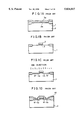
- FIGS. 5A to 5F show in a stepwise manner a first method for manufacturing a FET having the shaped gate electrode in accordance with the present invention.
- a P type semiconductor substrate 1 is prepared.
- a silicon oxide film 2 is formed on the main surface thereof (FIG. 5A).
- a lower layer 3a is formed on the silicon oxide film 2 and an upper layer 3b is formed thereon.
- a resist 11 is placed on a prescribed position on the upper layer 3b (FIG. 5B).
- the lower layer 3a and the upper layer 3b are etched by a known plasma etching method (FIG. 5C). The speed of etching of the lower layer 3a and the upper layer 3b are different from each other even under the same etching conditions.
- the etching speed of the lower layer 3a is faster than that of the upper layer 3b. Consequently, the amount of etching of the lower layer 3a in the transverse direction is greater than the amount of etching of the upper layer 3b (FIG. 5D). Consequently, after a prescribed time period, a shaped gate electrode such as shown in FIG. 5D is formed.
- the lower layer 3a and the upper layer 3b are preferably formed of the same base composition, i.e., polysilicon.
- these layers may contain a differing chemical or physical feature which provides the lower layer with a faster etch rate as compared with the upper layer etch rate.
- the lower and upper layers may be formed of polysilicon wherein the grain size of the polysilicon in the upper layer is different from that of the lower layer.
- the upper layer 3b may be formed of polysilicon having a 0.5 ⁇ grain size.
- Such a polysilicon layer may be formed by chemical vapor deposition at a temperature of about 650° C. to 700° C.
- the lower layer 3a may be formed of polysilicon having a grain size of from 1 to 2 ⁇ .
- a polysilicon layer may be formed by chemical vapor deposition at a temperature of about 580° C. to 600° C. The following etching conditions have then been employed to polysilicon layers 3a and 3b having differing grain sizes as described above:
- Electrode type parallel plate type RIE
- upper layer 3b formed of the polysilicon having the smaller grain size had an etch rate of about 1500 ⁇ /min while the lower layer 3a formed of polysilicon having the larger grain size had an etch rate of about 2500 ⁇ /min, i.e., approximately 1.7 times faster than that of the upper layer, thereby resulting in the formation of a shaped conductive layer gate electrode having an upper portion and lower portion with the upper portion being longer than the lower portion.
- the lower layer 3a may be provided with a faster etch rate than upper layer 3b by providing the upper layer with a first ion impurity concentration and the lower layer with a second ion impurity concentration wherein the second ion impurity concentration is greater than the first ion impurity concentration.
- the upper layer is provided with a phosphorous ion impurity concentration of about 1 ⁇ 10 15 /cm 3
- the lower layer is provided with a phosphorous ion impurity concentration of about 1 ⁇ 10 19 /cm 3
- the lower layer will have an etch rate which is approximately twice as fast (about 3,000 ⁇ /min as compared with about 1500 ⁇ /min) as compared with the upper layer.
- the upper and lower layers may be provided with different ion impurities wherein the ion impurities are selected so that the lower layer has a faster etch rate as compared with the upper layer.
- the lower layer is provided with a phosphorous ion impurity concentration of 1 ⁇ 10 15 /cm 3 , it would have an etch rate of about 1500 ⁇ /min while if the upper layer were provided with an arsenic ion impurity concentration of 1 ⁇ 10 15 /cm 3 , it would have an etch rate of about 1200 ⁇ /min.
- the upper and lower portions of the shaped conductive layer are formed of the same base composition, for example, polysilicon or a metal having a high melting point such as molybdenum silicon.
- the upper and lower layers from which the upper and lower portions of the shaped conductive layer are formed have a differing chemical or physical characteristic which provides the lower layer with a faster etch rate as compared with the upper layer so that the shaped conductive layer having an upper portion which is longer than the lower portion is formed in a single etching step.
- the lower layer is provided with a crystal defect which causes the etch rate of the lower layer to be faster as compared with that of the upper layer.
- the lower layer may be provided with a crystal defect by implanting Ar + as a neutral atom at a concentration of about 1 ⁇ 10 16 /cm 3 .
- the depth of the crystal defect can be controlled by selection of the implant energy in accordance with the thickness of the upper layer.
- the resulting etching rate of a lower polysilicon layer containing such a crystal defect is about 1650 ⁇ /min, which is about 10% faster than a similar polysilicon layer which does not contain the crystal defect provided by the Ar + implantation.
- Preferable conditions for etching in the method illustrated in FIG. 5 are, for example, as follows:
- the silicon oxide film 2 is removed, except for the portion below the gate electrode (FIG. 5E).
- the substrate is subjected to heat treatment at a high temperature. Consequently, impurity diffused layers 4a and 4b which are to be the source ⁇ drain, respectively, are formed on the main surface of the substrate (FIG. 5F).
- the gate electrode is shaped so that its upper portion is longer than its lower portion, and the lower portion which is adjacent the insulating film is substantially equal to or shorter than the length of the channel region at the main surface of the substrate. Therefore, an N type impurity region is not formed below the shaped gate electrode. Consequently, a method for manufacturing a FET is provided in which no additional capacitance is generated.
- the shaped conductive layer of the FET of the present invention may be produced from a single layer of material with the upper and lower portions of the shaped conductive layer being formed by two or more different etching steps which employ different etching conditions.
- This method is illustrated in FIGS. 6A-6D.
- the P type substrate 1 is provided with a silicon dioxide insulating layer 2 and a layer 3 from which the conductive layer is formed is provided on the silicon dioxide layer 2.
- a resist 11 is placed on a prescribed position of the layer 3.
- a first etching step employing normal etching conditions as described above is then conducted for a limited amount of time. This results in formation of the upper portion 3b of the shaped conductive layer serving as the gate electrode.
- the selection ratio between the resist mask and the etchant is about 1, and an organic polymer from the resist material adheres on the sidewalls of the etched layer during the etching. This is illustrated by reference numeral 3c in FIG. 6B. Since this adhesion layer 3c acts as a protection layer, etching of the portion 3b in the side or transverse direction is inhibited.
- etching steps are conducted in an isotropic manner whereby side etching or etching in the transverse direction takes place, resulting in the formation of the lower portion 3a of the shaped conductive layer.
- Suitable etching conditions for the second etch step are as follows:
- the shaped conductive layer gate electrode as shown in FIG. 6C is obtained since the lower portion of the polysilicon layer 3 is side etched in the isotropic second etching step.
- the base composition of the upper and lower layers which form the conductive layer and/or the etching conditions employed to form the shaped conductive layer may be varied in order to provide various shaped conductive layers wherein the upper portion of the shaped conductive layer is longer than the lower portion of the shaped conductive layer and the lower portion adjacent the insulating film is substantially equal to or shorter than the length of the channel region at the main surface in order to provide an improved FET according to the present invention.
- the FET of the invention having a shaped gate electrode is applied to a transistor of a LDD structure.
- a conventional transistor of a LDD structure is shown in FIG. 7C.
- the conventional transistor having a LDD structure comprises a P type semiconductor substrate 1, a gate electrode 3 formed on the main surface of the semiconductor substrate 1 with an insulating film interposed therebetween, an N type impurity diffused layer 4 of low concentration formed on the main surface of the semiconductor substrate, an N type impurity diffused layer 6 of high concentration, respectively, and side walls 5 formed on both sides of the gate electrode. Since the transistor having the LDD structure has two impurity layers of low concentration and high concentration, the high electric field near the drain is weakened. Consequently, the hot electron effect is suppressed. However, as in a common FET, the FET having the LDD structure has the problems of additional capacitance, the degradation of transconductance, and the like.
- FIGS. 7A to 7C The method for manufacturing a conventional FET having the LDD structure is shown in FIGS. 7A to 7C.
- a gate electrode 3 is formed on a P type semiconductor substrate with an insulating film 2 interposed therebetween.
- the gate electrode is formed by processing conductive materials such as polycrystalline silicon or a metal having a high melting point using a known method, for example, utilizing plasma reactance (FIG. 7A).
- Impurities of a second conductivity type are ion implanted on the main surface of the substrate 1 to a concentration of about 1 ⁇ 10 12 /cm 2 to 1 ⁇ 10 14 /cm 2 .
- N diffusion layers 4 are formed on both sides of the gate electrode 3 in self alignment using the gate electrode 3 as a mask.
- An oxide film such as a silicon oxide film is formed on the main surface of the semiconductor substrate 1 and on the gate electrode 3 to a prescribed thickness.
- the oxide film is etched by an anisotropic etching method such as ion etching having directivity. Consequently, silicon oxide films in the form of side walls 5 are formed on the side walls of the gate electrode 3.
- Impurities having the second conductivity type opposite to that of the substrate 1 are then ion implanted to a high concentration (no less than 1 ⁇ 10 14 /cm 2 ) using the side walls 5 and the gate electrode 3 as masks, and heat treatment is carried out at a high temperature. Consequently, activated source ⁇ drain diffused layers 6 are formed (FIG. 7C).
- the high concentration source ⁇ drain diffused layers 6 are formed in self alignment by using the side walls 5 as masks, so that the layers are formed towards the outer portions of the impurity diffused layers of low concentration.
- a conventional FET having the LDD structure is manufactured in the above described manner. Therefore, the conventional method comprises problems such as an increase in the steps for forming the side walls, and the difficulty in controlling the width of the side walls.
- FIGS. 8A to 8C A method for manufacturing a FET having the LDD structure utilizing the FET having a shaped gate electrode in accordance with the present invention is shown in FIGS. 8A to 8C.
- the process steps up to formation of the shaped gate electrode on the semiconductor substrate 1 with an insulating film interposed therebetween are the same as those shown in FIGS. 5A to 5E, or FIGS. 6A-6D, depending on the method of formation of the shaped gate electrode.
- the gate electrode 3 includes the lower portion 3a and the upper portion 3b as shown in FIG. 8A.
- Impurities having the second conductivity type, opposite to that of the substrate 1, are then ion implanted to a low concentration (1 ⁇ 10 12 /cm 2 to 1 ⁇ 10 14 /cm 2 ) from above the substrate by a known ion implantation technique using the gate electrode 3 as a mask.
- the substrate 1 is heat treated and low concentration source ⁇ drain diffused layers 4 are formed with the end portions thereof approaching the ends of the lower portion of the gate electrode 3 on the side of the substrate (FIG. 8A).
- an insulating film such as a silicon oxide film is formed on the main surface of the substrate 1, and on the gate electrode 3 to a prescribed thickness.
- An anisotropic etching method such as ion etching having directivity is carried out on the entire surface to form silicon oxide film side walls 5 on the side walls of the gate electrode 3 (FIG. 8B).
- impurities having the second conductivity type, opposite to that of the substrate 1 are ion implanted to a high concentration (more than 5 ⁇ 10 14 /cm 2 ) on the entire surface using the gate electrode 3 and the side walls 5 as masks.
- high concentration source ⁇ drain diffused layers 6 are formed (FIG. 8C).
- the high concentration source ⁇ drain diffused layers 6 are formed continuous to the low concentration source ⁇ drain diffused layers 4.
- the distance W4 between ends of the low concentration source ⁇ drain diffused layers 4 is narrower than the distance W6 between ends of the high concentration source ⁇ drain diffused layers 6. Consequently, a double diffusion structure is provided.
- the FET manufactured by the above described method comprises source ⁇ drain diffused layers of double diffusion structure consisting of low concentration diffused layers and high concentration diffused layers. Consequently, the electric field is weakened near the drain, whereby the generation of hot carriers can be suppressed. Even if the generated hot carriers are trapped in the insulating film 5, the negative potential of the electrons in the insulating film can be neutralized as described above, and consequently, the problem of degradation of transconductance due to the high resistance of the low concentration impurity layer 4 is prevented. Since the end of the above described low concentration impurity layer 4 is approximately aligned with the end of the lower portion of the gate electrode 3, any additional capacitance is hardly generated.
- the present invention can be applied to the N type or P type MOS transistors, and it can be applied to MOS transistors formed not only on the single substrate but on an epitaxial substrate or on a wafer. In either case, the same effect as described in the above embodiment can be obtained.
- the present invention is also applied to a compound semiconductor other than the silicon semiconductor.
- FIG. 9 is a plan view of a semiconductor memory device to which the FET of the present invention is applied.
- FIG. 10 is a cross sectional view taken along the line of FIG. 9.
- FIG. 11 is a partial enlarged view of the part designated by an arrow X in FIG. 10.
- the FET of the present invention can be easily incorporated with a semiconductor memory device. Accordingly, a semiconductor memory device whose operation speed is high can be easily provided.
- the length of the channel region is substantially equal to the length of the lower portion of the shaped gate electrode formed thereon, so that there is no overlapping portion between the lower portion of the gate electrode and the source ⁇ drain regions. Therefore, there will be no additional capacitance, and the speed of operation is increased.
- the potential in the upper layer portion of the shaped gate electrode neutralizes the electrons trapped therebelow, whereby the transconductance is not degraded.
- the shaped gate electrode comprises upper and lower portions, each of which is formed of the same base composition, and the gate electrode can be formed in one step of anisotropic etching as shown in FIG. 5D or in two or more etching steps, including an isotropic etching step, as shown in FIGS. 6A-6D. Therefore, the manufacturing can be carried out easily.
- the FET in accordance with the present invention comprises a T-shaped gate electrode consisting of upper and lower portions and source ⁇ drain regions having a channel region whose length is equal to or longer than the length of the lower portion of the shaped gate electrode. Consequently, a FET can be provided which is capable of high speed operation, in which the transconductance is not degraded and which can be manufactured easily.
Abstract
A field effect transistor comprises a semiconductor substrate having a main surface and a predetermined impurity concentration of a first conductivity type, impurity layers of a second conductivity type formed spaced apart at the main surface of the semiconductor substrate, and a shaped conductive layer serving as a gate electrode. The impurity layers constitute source·drain regions, and a region between the impurity layers defines a channel region in the main surface. The shaped conductive layer is formed on the channel region with an insulating film therebetween. The shaped conductive layer has an upper portion and a lower portion wherein the upper portion is longer than the lower portion and the length of the lower portion adjacent the insulating film is substantially equal to or shorter than the length of the channel region at the main surface. Additionally, the upper and lower portions of the shaped conductive layer are formed of the same base composition.
Description
This application is a continuation of application Ser. No. 07/787,912, filed Nov. 5, 1991, now U.S. Pat. No. 5,543,646 which is a continuation-in-part of application Ser. No. 07/242,116 filed Sep. 8, 1988, now U.S. Pat. No. 5,089,863.
The present invention relates generally to a field effect transistor and, more particularly, to a field effect transistor capable of high speed operation, and to manufacturing methods therefor.
Field effect transistors (hereinafter referred to as FET) are well known. FIGS. 1A to 1D show a conventional manufacturing process for a conventional FET in a stepwise manner. A silicon oxide film 2a is formed on a P type semiconductor substrate. A layer 3a of silicon or a conductive material such as a metal having a high melting point is formed on the silicon oxide film. (FIG. 1A). The polysilicon layer 3a and the silicon oxide film 2 are simultaneously etched by a known etching method, and a gate electrode 3 and a gate insulating film 2 are formed (FIG. 1B). A known etching method is disclosed in, for example, "Microfabrication Technique by Gas Plasma Etching Method," H. Komiya et al, Proc. of 7th Conference on Solid State Device 1975, Supplement to Japanese Journal of Applied Physics, Vol. 15, p. 19 (1976). N type impurities are implanted from above the semiconductor substrate 1 using the gate electrode 3 as a mask. Thereafter, a heat treatment is performed. Consequently, N+ impurity layers 4a and 4b are formed on a main surface of the semiconductor substrate 1 in self alignment. The N+ impurity layers 4a and 4b constitute a source and a drain of a transistor (FIG. 1C). An Al wiring layer is formed connected to the N+ impurity layers (FIG. 1D). An enlarged view of the gate portion of the FET transistor structure as described above is shown in FIG. 2A. Since the N+ impurity layers 4a and 4b are formed by heat treatment, the impurities are also diffused in the transverse direction in accordance with the diffusion coefficient of the impurities. Consequently, an overlap portion is generated between the gate electrode 3 and the source·drain diffusion layers 4. The degree of overlap (the distance ΔL) differs depending on the type of impurities and on the temperature of the heat treatment. An equivalent circuit of the device of FIG. 2A is shown in FIG. 2B.
The overlapping portion (ΔL) constitutes an additional capacitance between the gate and the source·drain as shown in the equivalent circuit of FIG. 2B. Therefore, if this MOS transistor is used in an integrated circuit or the like, the MOS transistor cannot operate at a high speed and the power consumption of the MOS transistor is relatively large. If the dimension of the overlapping portion is relatively large, a so-called short channel effect will occur, thereby causing problems such as a change in the threshold voltage of the MOS transistor. Therefore, the overlapping portion is also an obstruction in reducing the size of the MOS transistor.
In addition to the above described problem, the conventional FET also exhibits a decrease in transconductance. The transconductance is one of the characteristics of the transistor, which refers to the proportion of the drain current to the gate voltage. FIG. 3 is a schematic diagram showing the electric field and the movement of electrons in a conventional FET. The drain is maintained at a constant potential. A plane of equal potential is formed in the vicinity of the drain as shown in the figure. Therefore, an end portion of the drain has a high electric field. If a prescribed potential is applied to the gate of the transistor, a channel region is formed on the main surface of the semiconductor substrate between the source 4a and the drain 4b, whereby electrons move from the source 4a to the drain 4b. When the electrons reach the high electric field region near the drain, the electrons receive a large energy from the electric field, so that he electrons become hot electrons. The hot electrons generated in this manner are trapped near the gate insulating film sandwiched between the gate electrode and the drain region. Consequently, the surfaces of the drain and the channel region tend to invert to the p type. Therefore, the concentration of the N type impurities becomes substantially low and the source resistance of the MOS transistor increases. Normally, when a constant voltage is applied to the gate electrode of the FET, a constant current flows. However, due to the above described reasons, a constant current does not flow even if a constant voltage is applied to the gate.
Accordingly, an object of the present invention is to provide a FET which is capable of high speed operation, and to provide a method for manufacturing the same.
Another object of the present invention is to provide a FET in which the transconductance is not degraded, and to provide a manufacturing method therefor.
A further object of the present invention is to provide a FET which can be highly integrated, and to provide a manufacturing method therefor.
A still further object of the present invention is to provide a FET in which any additional capacitance constituted by a gate electrode and the source·drain electrode is not generated, and to provide a manufacturing method therefor.
A still further object of the present invention is to provide a FET in which the hot electron effect described above is not generated, and to provide a manufacturing method therefor.
A still further object of the present invention is to provide a FET having a lightly doped drain (hereinafter referred to as LDD) structure in which the transconductance is not degraded, and to provide a manufacturing method therefor.
A still further object of the present invention is to provide a FET having a LDD structure and which is capable of high speed operation, and to provide a manufacturing method therefor.
The above described objects of the present invention can be attained by a FET comprising a semiconductor substrate having a main surface and a predetermined impurity concentration of a first conductivity type, an impurity layer having a second conductivity type formed spaced apart on the main surface of the semiconductor substrate, the impurity layer constituting a source·drain region, and a region sandwiched by the impurity layers defining a channel region. The FET further comprises a shaped conductive layer, the upper portion of which is longer than the lower portion thereof. The conductive layer is formed on the channel region with an insulating film interposed therebetween. The length of the lower portion of the conductive layer which is adjacent the insulating film is equal to or shorter than the length of the channel region.
Since the FET comprises a shaped conductive layer as described as the gate electrode, the dimension of the overlapping portion between the source·drain region and the gate electrode is minimized. Therefore, the capacitance constituted by the source·drain region and the gate electrode is minimized. Consequently, a FET is provided which can operate at high speed and can be highly integrated.
Additionally, since the FET comprises a shaped gate electrode as described, the electrons existing below the eaves thereof generated by the hot electron effect are neutralized. Consequently, a FET is provided in which the transconductance is not degraded.
According to a preferred embodiment of the FET of the present invention, the impurity layer comprises a first impurity layer having a first concentration and a second impurity layer having a second concentration which is higher than the first concentration; a region sandwiched by the first impurity layers constituting a first channel region, and a region sandwiched by the second impurity layers constituting a second channel region. When the FET is structured in this manner, a FET having a shaped electrode of an LDD structure is provided. Consequently, a transistor having a LDD structure which is capable of high speed operation and in which the transconductance is not degraded is provided.
According to a further embodiment of the present invention, the method of manufacturing the FET containing the first and second impurity layers comprises the following additional steps. First, insulating side walls are formed on the end surfaces of the shaped conductive layer. The length of the side wall on the main surface of the semiconductor substrate is longer than the upper portion of the conductive layer, ions of the second conductivity type are doped on the main surface of the semiconductor substrate to a second concentration which is higher than the concentration of the first impurity layer using the shaped conductive layer with the insulating side walls formed thereon as a mask. Heat treatment of the doped semiconductor substrate is then conducted.
Since the method for manufacturing the FET comprises the above described steps, a method for manufacturing the FET of the LDD structure having a shaped electrode is provided. Consequently, a method for manufacturing a transistor of the LDD structure which is capable of high speed operation and in which the transconductance is not degraded is provided.
These objects and other objects, features, aspects and advantages of the present invention will become more apparent from the following detailed description of the present invention when taken in conjunction with the accompanying drawings.
FIGS. 1A to 1D show the manufacturing method of a conventional FET in a stepwise manner;
FIG. 2A is a diagram illustrating the additional capacitance existing in a conventional FET;
FIG. 2B is an equivalent circuit diagram of FIG. 2A;
FIG. 3 illustrates hot electron effect;
FIG. 4A shows the structure of a first embodiment of a FET in accordance with the present invention;
FIG. 4B illustrates the effect on the transconductance degradation of the FET of FIG. 4A in accordance with the present invention;
FIGS. 4C, 4D, 4E & 4F show the structures of additional embodiments of the gate structure in accordance with the present invention;
FIGS. 5A to 5F show in a stepwise manner a first method for manufacturing a FET in accordance with the present invention;
FIGS. 6A to 6D show a second method of forming the shaped conductive layer of the FET of the present invention;
FIGS. 7A-7C show in a stepwise manner a method for manufacturing a conventional FET having a LDD structure;
FIGS. 8A to 8C show in a stepwise manner a method for manufacturing a FET having a LDD structure in accordance with the present invention;
FIG. 9 is a plan view of a semiconductor memory device to which a FET of the present invention is applied;
FIG. 10 is a cross sectional view taken along the line IX--IX of FIG. 9; and
FIG. 11 is a partial enlarged view of FIG. 10.
FIG. 4A shows a sectional structure of a FET in accordance with the present invention. Referring to FIG. 4A, the FET in accordance with the present invention comprises a semiconductor substrate 1, a source region 4a and a drain region 4b formed on the main surface of the semiconductor substrate 1, and a shaped gate electrode 3 formed on the portion of the main surface of the semiconductor substrate between source region 4a and the drain region 4b with an insulating film 2 interposed between the gate electrode and the substrate main surface.
In the embodiment of FIG. 4A, the shaped conductive layer that forms the gate electrode 3 is T-shaped and comprises an upper portion 3b and a lower portion 3a, with the upper portion 3b being longer than the lower portion 3a.
Consequently, even if the impurity regions 4a and 4b are formed in self alignment by using the gate electrode as a mask, the end portions of the impurity regions are not formed below the lower portion of the gate electrode. The distance d between the eaves of the T and the main surface of the semiconductor substrate (see FIG. 4A) is large enough not to form a capacitance. Therefore, any additional capacitance such as shown in FIG. 2B will not be generated. Consequently, a FET capable of high speed operation is provided.
FIG. 4B illustrates the hot electron effect of the FET having the T-shaped gate electrode shown in FIG. 4A. Referring to FIG. 4B, the hot electrons generated by a high electric field do not degrade the transconductance in the FET having the T-shaped electrode for the following reasons. Namely, when the FET is in operation, the T-shaped gate electrode is maintained at a prescribed potential. The electrons move through the channel and turn to hot electrons by the high electric field and are trapped by the insulating film near the drain. However, since a positive potential is applied to the gate electrode as described above, the surface of the insulating film below the eaves of the T-shaped gate electrode has a positive potential. Therefore, the trapped hot electrons are neutralized and the surfaces of the drain and the channel regions are not inverted to the P type. If a constant voltage is applied to the gate electrode, a prescribed current flows. Consequently, a FET is provided in which the transconductance is not degraded.
FIGS. 4C-4F show additional embodiments of the FET according to the present invention containing a shaped conductive layer as a gate electrode. In all of the embodiments of FIGS. 4C-4F, the shaped conductive layer has an upper portion and a lower portion wherein the upper portion is longer than the lower portion and the length of the lower portion adjacent the insulating film is substantially equal to or shorter than the length of the channel region at the main surface of the semiconductor substrate. In the embodiments of FIGS. 4C and 4D, the lower portion 3a includes a section having tapered sidewalls and a section having vertical sidewalls. In the embodiments of FIGS. 4E and 4F, the sidewalls of the lower portion are tapered along their entire length. As in the embodiment set forth in FIG. 4A, even if the impurity regions 4a and 4b of the FET's of FIGS. 4C-4F are formed in self alignment by using the gate electrode as a mask, the end portions of the impurity regions are not formed below the lower portion of the gate electrode. The distance d between the eaves of the upper portion of the gate electrode and the main surface of the semiconductor substrate in each of the FET's of FIGS. 4C-4F is sufficiently large not to form a capacitance. Therefore, any additional capacitance such as shown in FIG. 2B will not be generated and FET's capable of high speed operation are provided.
FIGS. 5A to 5F show in a stepwise manner a first method for manufacturing a FET having the shaped gate electrode in accordance with the present invention. A P type semiconductor substrate 1 is prepared. A silicon oxide film 2 is formed on the main surface thereof (FIG. 5A). A lower layer 3a is formed on the silicon oxide film 2 and an upper layer 3b is formed thereon. A resist 11 is placed on a prescribed position on the upper layer 3b (FIG. 5B). The lower layer 3a and the upper layer 3b are etched by a known plasma etching method (FIG. 5C). The speed of etching of the lower layer 3a and the upper layer 3b are different from each other even under the same etching conditions. That is, the etching speed of the lower layer 3a is faster than that of the upper layer 3b. Consequently, the amount of etching of the lower layer 3a in the transverse direction is greater than the amount of etching of the upper layer 3b (FIG. 5D). Consequently, after a prescribed time period, a shaped gate electrode such as shown in FIG. 5D is formed.
More particularly, the lower layer 3a and the upper layer 3b are preferably formed of the same base composition, i.e., polysilicon. However, in this embodiment, it is preferred that these layers contain a differing chemical or physical feature which provides the lower layer with a faster etch rate as compared with the upper layer etch rate. For example, the lower and upper layers may be formed of polysilicon wherein the grain size of the polysilicon in the upper layer is different from that of the lower layer. With reference to FIG. 5B, the upper layer 3b may be formed of polysilicon having a 0.5μ grain size. Such a polysilicon layer may be formed by chemical vapor deposition at a temperature of about 650° C. to 700° C. On the other hand, the lower layer 3a may be formed of polysilicon having a grain size of from 1 to 2μ. Such a polysilicon layer may be formed by chemical vapor deposition at a temperature of about 580° C. to 600° C. The following etching conditions have then been employed to polysilicon layers 3a and 3b having differing grain sizes as described above:
(i) Reaction gas: Cl2 and O2 (5%)
(ii) Flow rate: 70 sccm (70 cc per minute; sccm is standard cubic per cm)
(iii) Pressure: 150 mTorr
(iv) Power: 0.2 Watt/cm2
(v) Plate temperature: 20° C.
(vi) Electrode type: parallel plate type RIE
(Cathode Coupling Type wherein RF is applied to the lower electrode on the wafer side)
As a result, upper layer 3b formed of the polysilicon having the smaller grain size had an etch rate of about 1500 Å/min while the lower layer 3a formed of polysilicon having the larger grain size had an etch rate of about 2500 Å/min, i.e., approximately 1.7 times faster than that of the upper layer, thereby resulting in the formation of a shaped conductive layer gate electrode having an upper portion and lower portion with the upper portion being longer than the lower portion.
Similarly, the lower layer 3a may be provided with a faster etch rate than upper layer 3b by providing the upper layer with a first ion impurity concentration and the lower layer with a second ion impurity concentration wherein the second ion impurity concentration is greater than the first ion impurity concentration. For example, if the upper layer is provided with a phosphorous ion impurity concentration of about 1×10¹⁵ /cm3, and the lower layer is provided with a phosphorous ion impurity concentration of about 1×10¹⁹ /cm3, the lower layer will have an etch rate which is approximately twice as fast (about 3,000 Å/min as compared with about 1500 Å/min) as compared with the upper layer. In a further embodiment, the upper and lower layers may be provided with different ion impurities wherein the ion impurities are selected so that the lower layer has a faster etch rate as compared with the upper layer. For example, if the lower layer is provided with a phosphorous ion impurity concentration of 1×10¹⁵ /cm3, it would have an etch rate of about 1500 Å/min while if the upper layer were provided with an arsenic ion impurity concentration of 1×10¹⁵ /cm3, it would have an etch rate of about 1200 Å/min.
Thus, in this first embodiment of making a field effect transistor having a shaped conductive layer according to the present invention, the upper and lower portions of the shaped conductive layer are formed of the same base composition, for example, polysilicon or a metal having a high melting point such as molybdenum silicon. However, the upper and lower layers from which the upper and lower portions of the shaped conductive layer are formed have a differing chemical or physical characteristic which provides the lower layer with a faster etch rate as compared with the upper layer so that the shaped conductive layer having an upper portion which is longer than the lower portion is formed in a single etching step.
In a further embodiment of forming the shaped conductive layer from upper and lower layers having the same base composition, the lower layer is provided with a crystal defect which causes the etch rate of the lower layer to be faster as compared with that of the upper layer. For example, the lower layer may be provided with a crystal defect by implanting Ar+ as a neutral atom at a concentration of about 1×10¹⁶ /cm3. As is well known in the art, the depth of the crystal defect can be controlled by selection of the implant energy in accordance with the thickness of the upper layer. The resulting etching rate of a lower polysilicon layer containing such a crystal defect is about 1650 Å/min, which is about 10% faster than a similar polysilicon layer which does not contain the crystal defect provided by the Ar+ implantation.
Preferable conditions for etching in the method illustrated in FIG. 5 are, for example, as follows:
gas composition: carbon fluoride CF4 (99%) and oxygen O2 (1%)
power: radio frequency 20-200 W
gas pressure: 0.3-0.7 Torr
After formation of the gate electrode, the silicon oxide film 2 is removed, except for the portion below the gate electrode (FIG. 5E). After N type impurities are doped from above the substrate using the shaped gate electrode as a mask, the substrate is subjected to heat treatment at a high temperature. Consequently, impurity diffused layers 4a and 4b which are to be the source·drain, respectively, are formed on the main surface of the substrate (FIG. 5F). The gate electrode is shaped so that its upper portion is longer than its lower portion, and the lower portion which is adjacent the insulating film is substantially equal to or shorter than the length of the channel region at the main surface of the substrate. Therefore, an N type impurity region is not formed below the shaped gate electrode. Consequently, a method for manufacturing a FET is provided in which no additional capacitance is generated.
In a second manufacturing embodiment, the shaped conductive layer of the FET of the present invention may be produced from a single layer of material with the upper and lower portions of the shaped conductive layer being formed by two or more different etching steps which employ different etching conditions. This method is illustrated in FIGS. 6A-6D. With reference to FIG. 6A, the P type substrate 1 is provided with a silicon dioxide insulating layer 2 and a layer 3 from which the conductive layer is formed is provided on the silicon dioxide layer 2. A resist 11 is placed on a prescribed position of the layer 3. A first etching step employing normal etching conditions as described above is then conducted for a limited amount of time. This results in formation of the upper portion 3b of the shaped conductive layer serving as the gate electrode. Under normal etching conditions as described above, the selection ratio between the resist mask and the etchant is about 1, and an organic polymer from the resist material adheres on the sidewalls of the etched layer during the etching. This is illustrated by reference numeral 3c in FIG. 6B. Since this adhesion layer 3c acts as a protection layer, etching of the portion 3b in the side or transverse direction is inhibited.
After completion of the first etch step, one or more additional etch steps are conducted in an isotropic manner whereby side etching or etching in the transverse direction takes place, resulting in the formation of the lower portion 3a of the shaped conductive layer. Suitable etching conditions for the second etch step are as follows:
(i) Reaction gas: SF6 (100%)
(ii) Flow rate: 120 sccm
(iii) Pressure: 800 mTorr
(iv) Power: 0.15 watt·cm2
(v) Electrode type: parallel plate type RIE
(anode coupling type wherein RF is applied to the upper opposite electrode).
If a polysilicon layer 3 is etched at a rate of about 2,000 Å/min under the normal etching conditions described above as the first etching step, and the new etching conditions as described above are employed in a second etching step, the shaped conductive layer gate electrode as shown in FIG. 6C is obtained since the lower portion of the polysilicon layer 3 is side etched in the isotropic second etching step.
Additionally, in the isotropic etching step as described above, when silicon dioxide is used as the insulating film under a polysilicon layer, a phenomenon occurs wherein the polysilicon near the interface of the polysilicon layer 3 and the silicon dioxide insulating layer 2 is excessively etched due to the reflection of the reactive ion, i.e., fluorine radicals, from the silicon dioxide insulating film during the final etching stage. Additionally, the effect of this excessive etching is increased when the silicon dioxide insulating film is inclined as shown in FIG. 6D. Thus, the use of an inclined silicon dioxide insulating film as shown in FIG. 6D is advantageous when a wedge-shaped lower portion in the shaped conductive layer is desired.
Thus, it would be apparent to one of ordinary skill in the art that the base composition of the upper and lower layers which form the conductive layer and/or the etching conditions employed to form the shaped conductive layer may be varied in order to provide various shaped conductive layers wherein the upper portion of the shaped conductive layer is longer than the lower portion of the shaped conductive layer and the lower portion adjacent the insulating film is substantially equal to or shorter than the length of the channel region at the main surface in order to provide an improved FET according to the present invention.
The FET of the invention having a shaped gate electrode is applied to a transistor of a LDD structure. A conventional transistor of a LDD structure is shown in FIG. 7C. Referring to FIG. 7C, the conventional transistor having a LDD structure comprises a P type semiconductor substrate 1, a gate electrode 3 formed on the main surface of the semiconductor substrate 1 with an insulating film interposed therebetween, an N type impurity diffused layer 4 of low concentration formed on the main surface of the semiconductor substrate, an N type impurity diffused layer 6 of high concentration, respectively, and side walls 5 formed on both sides of the gate electrode. Since the transistor having the LDD structure has two impurity layers of low concentration and high concentration, the high electric field near the drain is weakened. Consequently, the hot electron effect is suppressed. However, as in a common FET, the FET having the LDD structure has the problems of additional capacitance, the degradation of transconductance, and the like.
The method for manufacturing a conventional FET having the LDD structure is shown in FIGS. 7A to 7C. A gate electrode 3 is formed on a P type semiconductor substrate with an insulating film 2 interposed therebetween. The gate electrode is formed by processing conductive materials such as polycrystalline silicon or a metal having a high melting point using a known method, for example, utilizing plasma reactance (FIG. 7A).
Impurities of a second conductivity type are ion implanted on the main surface of the substrate 1 to a concentration of about 1×10¹² /cm2 to 1×10¹⁴ /cm2. On this occasion, N diffusion layers 4 are formed on both sides of the gate electrode 3 in self alignment using the gate electrode 3 as a mask.
An oxide film such as a silicon oxide film is formed on the main surface of the semiconductor substrate 1 and on the gate electrode 3 to a prescribed thickness. The oxide film is etched by an anisotropic etching method such as ion etching having directivity. Consequently, silicon oxide films in the form of side walls 5 are formed on the side walls of the gate electrode 3. Impurities having the second conductivity type opposite to that of the substrate 1 are then ion implanted to a high concentration (no less than 1×10¹⁴ /cm2) using the side walls 5 and the gate electrode 3 as masks, and heat treatment is carried out at a high temperature. Consequently, activated source·drain diffused layers 6 are formed (FIG. 7C). The high concentration source·drain diffused layers 6 are formed in self alignment by using the side walls 5 as masks, so that the layers are formed towards the outer portions of the impurity diffused layers of low concentration.
A conventional FET having the LDD structure is manufactured in the above described manner. Therefore, the conventional method comprises problems such as an increase in the steps for forming the side walls, and the difficulty in controlling the width of the side walls.
A method for manufacturing a FET having the LDD structure utilizing the FET having a shaped gate electrode in accordance with the present invention is shown in FIGS. 8A to 8C. The process steps up to formation of the shaped gate electrode on the semiconductor substrate 1 with an insulating film interposed therebetween are the same as those shown in FIGS. 5A to 5E, or FIGS. 6A-6D, depending on the method of formation of the shaped gate electrode. The gate electrode 3 includes the lower portion 3a and the upper portion 3b as shown in FIG. 8A.
Impurities having the second conductivity type, opposite to that of the substrate 1, are then ion implanted to a low concentration (1×10¹² /cm2 to 1×10¹⁴ /cm2) from above the substrate by a known ion implantation technique using the gate electrode 3 as a mask. The substrate 1 is heat treated and low concentration source·drain diffused layers 4 are formed with the end portions thereof approaching the ends of the lower portion of the gate electrode 3 on the side of the substrate (FIG. 8A).
Thereafter, an insulating film such as a silicon oxide film is formed on the main surface of the substrate 1, and on the gate electrode 3 to a prescribed thickness. An anisotropic etching method such as ion etching having directivity is carried out on the entire surface to form silicon oxide film side walls 5 on the side walls of the gate electrode 3 (FIG. 8B).
Thereafter, impurities having the second conductivity type, opposite to that of the substrate 1, are ion implanted to a high concentration (more than 5×10¹⁴ /cm2) on the entire surface using the gate electrode 3 and the side walls 5 as masks. By the heat treatment of the substrate, high concentration source·drain diffused layers 6 are formed (FIG. 8C). On this occasion, the high concentration source·drain diffused layers 6 are formed continuous to the low concentration source·drain diffused layers 4. The distance W4 between ends of the low concentration source·drain diffused layers 4 is narrower than the distance W6 between ends of the high concentration source·drain diffused layers 6. Consequently, a double diffusion structure is provided.
The FET manufactured by the above described method comprises source·drain diffused layers of double diffusion structure consisting of low concentration diffused layers and high concentration diffused layers. Consequently, the electric field is weakened near the drain, whereby the generation of hot carriers can be suppressed. Even if the generated hot carriers are trapped in the insulating film 5, the negative potential of the electrons in the insulating film can be neutralized as described above, and consequently, the problem of degradation of transconductance due to the high resistance of the low concentration impurity layer 4 is prevented. Since the end of the above described low concentration impurity layer 4 is approximately aligned with the end of the lower portion of the gate electrode 3, any additional capacitance is hardly generated.
The present invention can be applied to the N type or P type MOS transistors, and it can be applied to MOS transistors formed not only on the single substrate but on an epitaxial substrate or on a wafer. In either case, the same effect as described in the above embodiment can be obtained. The present invention is also applied to a compound semiconductor other than the silicon semiconductor.
A semiconductor memory device to which the FET in accordance with the present invention is applied will be explained. FIG. 9 is a plan view of a semiconductor memory device to which the FET of the present invention is applied. FIG. 10 is a cross sectional view taken along the line of FIG. 9. FIG. 11 is a partial enlarged view of the part designated by an arrow X in FIG. 10.
Referring to FIGS. 9 to 11, the FET of the present invention can be easily incorporated with a semiconductor memory device. Accordingly, a semiconductor memory device whose operation speed is high can be easily provided.
In the FET in accordance with the present invention, the length of the channel region is substantially equal to the length of the lower portion of the shaped gate electrode formed thereon, so that there is no overlapping portion between the lower portion of the gate electrode and the source·drain regions. Therefore, there will be no additional capacitance, and the speed of operation is increased. The potential in the upper layer portion of the shaped gate electrode neutralizes the electrons trapped therebelow, whereby the transconductance is not degraded.
In accordance with the methods for manufacturing the FET of the present invention, the shaped gate electrode comprises upper and lower portions, each of which is formed of the same base composition, and the gate electrode can be formed in one step of anisotropic etching as shown in FIG. 5D or in two or more etching steps, including an isotropic etching step, as shown in FIGS. 6A-6D. Therefore, the manufacturing can be carried out easily.
As described above, the FET in accordance with the present invention comprises a T-shaped gate electrode consisting of upper and lower portions and source·drain regions having a channel region whose length is equal to or longer than the length of the lower portion of the shaped gate electrode. Consequently, a FET can be provided which is capable of high speed operation, in which the transconductance is not degraded and which can be manufactured easily.
Although the present invention has been described and illustrated in detail, it is clearly understood that the same is by way of illustration and example only and is not to be taken by way of limitation, the spirit and scope of the present invention being limited only by the terms of the appended claims.
Claims (5)
1. A field effect transistor comprising:
a semiconductor substrate having a main surface and a predetermined impurity concentration of a first conductivity type;
impurity layers of a second conductivity type formed spaced apart at the main surface of the semiconductor substrate, said impurity layers constituting source-drain regions, each of the impurity layers comprising a first impurity layer portion having a first impurity concentration and a second impurity layer portion having a second impurity concentration which is higher than the first impurity concentration, the first impurity layer portions defining a first channel region at the main surface of the substrate and the second impurity layer portions defining a second channel region, the first impurity layer portions being shallower throughout the substrate as compared with the second impurity layer portions; and
a shaped conductive layer formed by etching on said first channel region with an insulating film interposed therebetween at said main surface, said shaped conductive layer having an upper portion and a lower portion, the upper portion having a flat upper surface and being longer than the lower portion, the length of the lower portion adjacent the insulating film being substantially equal to or shorter than the length of said first channel region, the width of the second channel region being no greater than the length of the upper portion upper surface, and the upper and lower portions being formed of the same material, with the lower portion having a faster etch rate as compared with an etch rate of the upper portion under the same etching conditions, and wherein there is only insulating film between outermost ends of the shaped conductive layer upper portion and the main surface of the substrate, wherein the lower portion of the shaped conductive layer includes a section having tapered side walls.
2. A field effect transistor as defined by claim 1, wherein the shaped conductive layer is T-shaped.
3. A field effect transistor as defined by claim 1, wherein the lower portion further includes a section having vertical side walls.
4. A field effect transistor as defined by claim 1, wherein the upper and lower portions of the shaped conductive layer are formed of polysilicon.
5. A field effect transistor as defined by claim 1, wherein the distance between the upper portion and the main surface of the substrate is greater than the distance between the lower portion and the main surface of the substrate.
Priority Applications (1)
| Application Number | Priority Date | Filing Date | Title |
|---|---|---|---|
| US07/983,931 US5834817A (en) | 1988-09-08 | 1992-12-01 | Field effect transistor with a shaped gate electrode |
Applications Claiming Priority (3)
| Application Number | Priority Date | Filing Date | Title |
|---|---|---|---|
| US07/242,116 US5089863A (en) | 1988-09-08 | 1988-09-08 | Field effect transistor with T-shaped gate electrode |
| US07/787,912 US5543646A (en) | 1988-09-08 | 1991-11-05 | Field effect transistor with a shaped gate electrode |
| US07/983,931 US5834817A (en) | 1988-09-08 | 1992-12-01 | Field effect transistor with a shaped gate electrode |
Related Parent Applications (1)
| Application Number | Title | Priority Date | Filing Date |
|---|---|---|---|
| US07/787,912 Continuation US5543646A (en) | 1988-09-08 | 1991-11-05 | Field effect transistor with a shaped gate electrode |
Publications (1)
| Publication Number | Publication Date |
|---|---|
| US5834817A true US5834817A (en) | 1998-11-10 |
Family
ID=26934842
Family Applications (3)
| Application Number | Title | Priority Date | Filing Date |
|---|---|---|---|
| US07/787,912 Expired - Fee Related US5543646A (en) | 1988-09-08 | 1991-11-05 | Field effect transistor with a shaped gate electrode |
| US07/968,941 Expired - Fee Related US5650342A (en) | 1988-09-08 | 1992-10-30 | Method of making a field effect transistor with a T shaped polysilicon gate electrode |
| US07/983,931 Expired - Fee Related US5834817A (en) | 1988-09-08 | 1992-12-01 | Field effect transistor with a shaped gate electrode |
Family Applications Before (2)
| Application Number | Title | Priority Date | Filing Date |
|---|---|---|---|
| US07/787,912 Expired - Fee Related US5543646A (en) | 1988-09-08 | 1991-11-05 | Field effect transistor with a shaped gate electrode |
| US07/968,941 Expired - Fee Related US5650342A (en) | 1988-09-08 | 1992-10-30 | Method of making a field effect transistor with a T shaped polysilicon gate electrode |
Country Status (1)
| Country | Link |
|---|---|
| US (3) | US5543646A (en) |
Cited By (25)
| Publication number | Priority date | Publication date | Assignee | Title |
|---|---|---|---|---|
| US6018179A (en) * | 1998-11-05 | 2000-01-25 | Advanced Micro Devices | Transistors having a scaled channel length and integrated spacers with enhanced silicidation properties |
| US6037630A (en) * | 1997-05-26 | 2000-03-14 | Mitsubishi Denki Kabushiki Kaisha | Semiconductor device with gate electrode portion and method of manufacturing the same |
| WO2000034984A2 (en) * | 1998-12-07 | 2000-06-15 | Intel Corporation | Transistor with notched gate |
| US6191044B1 (en) * | 1998-10-08 | 2001-02-20 | Advanced Micro Devices, Inc. | Method for forming graded LDD transistor using controlled polysilicon gate profile |
| US6303410B1 (en) | 1998-06-01 | 2001-10-16 | North Carolina State University | Methods of forming power semiconductor devices having T-shaped gate electrodes |
| US6306710B1 (en) * | 2000-02-03 | 2001-10-23 | Advanced Micro Devices, Inc. | Fabrication of a gate structures having a longer length toward the top for formation of a rectangular shaped spacer |
| US6329230B1 (en) * | 1998-06-11 | 2001-12-11 | Fujitsu Quantum Devices Limited | High-speed compound semiconductor device having an improved gate structure |
| FR2811474A1 (en) * | 2000-07-07 | 2002-01-11 | Commissariat Energie Atomique | METHOD FOR MAKING A GRID FOR A CHANNEL TRANSISTOR STRUCTURE WITH A CHANNEL OF REDUCED LENGTH |
| US20020079525A1 (en) * | 2000-12-26 | 2002-06-27 | Nec Corporation | Semiconductor device and method of fabricating the same |
| WO2002069383A2 (en) * | 2001-02-22 | 2002-09-06 | Applied Materials, Inc. | Method of forming a notched silicon-containing gate structure |
| US6475841B1 (en) * | 2000-06-02 | 2002-11-05 | Motorola, Inc. | Transistor with shaped gate electrode and method therefor |
| US6509219B2 (en) * | 2001-03-19 | 2003-01-21 | International Business Machines Corporation | Fabrication of notched gates by passivating partially etched gate sidewalls and then using an isotropic etch |
| US6524901B1 (en) * | 2002-06-20 | 2003-02-25 | Micron Technology, Inc. | Method for forming a notched damascene planar poly/metal gate |
| US6528363B2 (en) * | 2001-03-19 | 2003-03-04 | International Business Machines Corporation | Fabrication of notched gates by passivating partially etched gate sidewalls and then using an isotropic etch |
| US6624483B2 (en) * | 2000-07-12 | 2003-09-23 | Fujitsu Limited | Semiconductor device having an insulated gate and a fabrication process thereof |
| US20040185623A1 (en) * | 2003-03-19 | 2004-09-23 | Taiwan Semiconductor Manaufacturing Co. | System-on-chip (SOC) solutions with multiple devices by multiple poly gate trimming process |
| JP2004343014A (en) * | 2003-05-19 | 2004-12-02 | Sharp Corp | Semiconductor memory, semiconductor device, and their manufacturing method, portable electronic apparatus, and ic card |
| US20050202642A1 (en) * | 2004-03-11 | 2005-09-15 | Taiwan Semiconductor Manufacturing Co. | Method of forming polysilicon gate structures with specific edge profiles for optimization of LDD offset spacing |
| US20050215008A1 (en) * | 2004-03-26 | 2005-09-29 | Orlowski Marius K | Method for forming a semiconductor device having a notched control electrode and structure thereof |
| US7078284B2 (en) | 2002-06-20 | 2006-07-18 | Micron Technology, Inc. | Method for forming a notched gate |
| US20060234449A1 (en) * | 2004-10-14 | 2006-10-19 | Smayling Michael C | Flash gate stack notch to improve coupling ratio |
| CN1295755C (en) * | 2003-10-27 | 2007-01-17 | 上海宏力半导体制造有限公司 | Method for forming grooved grid structure |
| US20070166902A1 (en) * | 2006-01-13 | 2007-07-19 | Orlowski Marius K | Method to control the gate sidewall profile by graded material composition |
| US20120086056A1 (en) * | 2010-10-08 | 2012-04-12 | Globalfoundries Inc. | Superior Integrity of a High-K Gate Stack by Forming a Controlled Undercut on the Basis of a Wet Chemistry |
| US20130059435A1 (en) * | 2011-09-01 | 2013-03-07 | Tao Yang | Method of Manufacturing Dummy Gates in Gate Last Process |
Families Citing this family (16)
| Publication number | Priority date | Publication date | Assignee | Title |
|---|---|---|---|---|
| JP3009975B2 (en) * | 1992-11-30 | 2000-02-14 | シャープ株式会社 | Dry etching method for silicon thin film |
| KR100359795B1 (en) * | 1995-08-22 | 2003-01-14 | 엘지.필립스 엘시디 주식회사 | Liquid crystal display and method for fabricating the same |
| US5612234A (en) * | 1995-10-04 | 1997-03-18 | Lg Electronics Inc. | Method for manufacturing a thin film transistor |
| US5763285A (en) * | 1996-06-10 | 1998-06-09 | Winbond Electronics Corporation | Process for controlling gate/drain overlapped length in lightly-doped drain (LDD) structures |
| US6010954A (en) * | 1997-07-11 | 2000-01-04 | Chartered Semiconductor Manufacturing, Ltd. | Cmos gate architecture for integration of salicide process in sub 0.1 . .muM devices |
| KR19990030993A (en) * | 1997-10-08 | 1999-05-06 | 윤종용 | Most transistor structure for high speed operation |
| US6013570A (en) * | 1998-07-17 | 2000-01-11 | Advanced Micro Devices, Inc. | LDD transistor using novel gate trim technique |
| US6137145A (en) * | 1999-01-26 | 2000-10-24 | Advanced Micro Devices, Inc. | Semiconductor topography including integrated circuit gate conductors incorporating dual layers of polysilicon |
| FR2791177A1 (en) * | 1999-03-19 | 2000-09-22 | France Telecom | PROCESS FOR PRODUCING A MUSHROOM GRILLE OR "T" GRILLE |
| US6596598B1 (en) * | 2000-02-23 | 2003-07-22 | Advanced Micro Devices, Inc. | T-shaped gate device and method for making |
| US6891235B1 (en) * | 2000-11-15 | 2005-05-10 | International Business Machines Corporation | FET with T-shaped gate |
| US6376351B1 (en) | 2001-06-28 | 2002-04-23 | Taiwan Semiconductor Manufacturing Company | High Fmax RF MOSFET with embedded stack gate |
| US6905976B2 (en) * | 2003-05-06 | 2005-06-14 | International Business Machines Corporation | Structure and method of forming a notched gate field effect transistor |
| US7365015B2 (en) * | 2004-07-13 | 2008-04-29 | Lsi Logic Corporation | Damascene replacement metal gate process with controlled gate profile and length using Si1-xGex as sacrificial material |
| CN102479691A (en) * | 2010-11-30 | 2012-05-30 | 中芯国际集成电路制造(上海)有限公司 | Forming methods of metal gate and MOS (Metal Oxide Semiconductor) transistor |
| US11127831B2 (en) | 2019-09-24 | 2021-09-21 | Globalfoundries U.S. Inc. | Transistor structure with overlying gate on polysilicon gate structure and related method |
Citations (39)
| Publication number | Priority date | Publication date | Assignee | Title |
|---|---|---|---|---|
| US4038107A (en) * | 1975-12-03 | 1977-07-26 | Burroughs Corporation | Method for making transistor structures |
| JPS5372578A (en) * | 1976-12-10 | 1978-06-28 | Fujitsu Ltd | Mis-type field effect transistor |
| US4102733A (en) * | 1977-04-29 | 1978-07-25 | International Business Machines Corporation | Two and three mask process for IGFET fabrication |
| JPS54108582A (en) * | 1978-02-15 | 1979-08-25 | Toshiba Corp | Manufacture of silicon type field effect transistor |
| JPS5583267A (en) * | 1978-12-20 | 1980-06-23 | Matsushita Electric Ind Co Ltd | Method of fabricating semiconductor device |
| US4417385A (en) * | 1982-08-09 | 1983-11-29 | General Electric Company | Processes for manufacturing insulated-gate semiconductor devices with integral shorts |
| US4419810A (en) * | 1981-12-30 | 1983-12-13 | International Business Machines Corporation | Self-aligned field effect transistor process |
| US4419809A (en) * | 1981-12-30 | 1983-12-13 | International Business Machines Corporation | Fabrication process of sub-micrometer channel length MOSFETs |
| US4430792A (en) * | 1982-07-08 | 1984-02-14 | General Electric Company | Minimal mask process for manufacturing insulated-gate semiconductor devices with integral shorts |
| JPS5934663A (en) * | 1982-08-21 | 1984-02-25 | Mitsubishi Electric Corp | Mis field effect type transistor |
| JPS5946084A (en) * | 1982-09-09 | 1984-03-15 | Mitsubishi Electric Corp | Field effect transistor and manufacture thereof |
| JPS59115554A (en) * | 1982-12-22 | 1984-07-04 | Toshiba Corp | Semiconductor device and manufacture thereof |
| US4476482A (en) * | 1981-05-29 | 1984-10-09 | Texas Instruments Incorporated | Silicide contacts for CMOS devices |
| GB2138632A (en) * | 1983-03-31 | 1984-10-24 | Ates Componenti Elettron | Self-aligned double layers of poly-crystalline silicon |
| JPS60229374A (en) * | 1984-04-27 | 1985-11-14 | Toshiba Corp | Semiconductor device and manufacture thereof |
| US4577391A (en) * | 1984-07-27 | 1986-03-25 | Monolithic Memories, Inc. | Method of manufacturing CMOS devices |
| US4592128A (en) * | 1984-06-04 | 1986-06-03 | Inmos Corporation | Method for fabricating integrated circuits with polysilicon resistors |
| WO1986006877A1 (en) * | 1985-05-03 | 1986-11-20 | American Telephone & Telegraph Company | Polycide process in semiconductor fabrication |
| DE3709708A1 (en) * | 1986-03-31 | 1987-10-08 | Toshiba Kawasaki Kk | FIELD EFFECT TRANSISTOR WITH LOW DOPED DRAIN ARRANGEMENT AND METHOD FOR PRODUCING THE SAME |
| JPS62242366A (en) * | 1986-04-14 | 1987-10-22 | Nec Corp | Semiconductor device |
| JPS6344770A (en) * | 1986-08-12 | 1988-02-25 | Mitsubishi Electric Corp | Field effect transistor and manufacture of the same |
| JPS6344771A (en) * | 1986-08-12 | 1988-02-25 | Mitsubishi Electric Corp | Semiconductor integrated circuit device and manufacture thereof |
| US4745086A (en) * | 1985-09-26 | 1988-05-17 | Motorola, Inc. | Removable sidewall spacer for lightly doped drain formation using one mask level and differential oxidation |
| JPS63131575A (en) * | 1986-11-21 | 1988-06-03 | Toshiba Corp | Mos transistor and manufacture thereof |
| JPS63204772A (en) * | 1987-02-20 | 1988-08-24 | Sharp Corp | Manufacture of semiconductor device |
| US4795716A (en) * | 1987-06-19 | 1989-01-03 | General Electric Company | Method of making a power IC structure with enhancement and/or CMOS logic |
| US4845046A (en) * | 1986-09-02 | 1989-07-04 | Seiko Instruments Inc. | Process for producing semiconductor devices by self-alignment technology |
| US4845534A (en) * | 1981-01-30 | 1989-07-04 | Fujitsu Limited | Field effect semiconductor device |
| US4869781A (en) * | 1987-10-30 | 1989-09-26 | International Business Machines Corporation | Method for fabricating a semiconductor integrated circuit structure having a submicrometer length device element |
| US4907048A (en) * | 1987-11-23 | 1990-03-06 | Xerox Corporation | Double implanted LDD transistor self-aligned with gate |
| US4908327A (en) * | 1988-05-02 | 1990-03-13 | Texas Instruments, Incorporated | Counter-doped transistor |
| JPH0281632A (en) * | 1988-09-20 | 1990-03-22 | Toshiba Mach Co Ltd | Register error detector |
| US4925807A (en) * | 1988-06-30 | 1990-05-15 | Kabushiki Kaisha Toshiba | Method of manufacturing a semiconductor device |
| US4933994A (en) * | 1987-06-11 | 1990-06-19 | General Electric Company | Method for fabricating a self-aligned lightly doped drain semiconductor device with silicide |
| US4978626A (en) * | 1988-09-02 | 1990-12-18 | Motorola, Inc. | LDD transistor process having doping sensitive endpoint etching |
| US4985745A (en) * | 1988-01-05 | 1991-01-15 | Kabushiki Kaisha Toshiba | Substrate structure for composite semiconductor device |
| US5024960A (en) * | 1987-06-16 | 1991-06-18 | Texas Instruments Incorporated | Dual LDD submicron CMOS process for making low and high voltage transistors with common gate |
| US5081052A (en) * | 1986-06-25 | 1992-01-14 | Hitachi, Ltd. | ROM and process for producing the same |
| US5089863A (en) * | 1988-09-08 | 1992-02-18 | Mitsubishi Denki Kabushiki Kaisha | Field effect transistor with T-shaped gate electrode |
Family Cites Families (7)
| Publication number | Priority date | Publication date | Assignee | Title |
|---|---|---|---|---|
| JPS6344768A (en) * | 1986-08-12 | 1988-02-25 | Mitsubishi Electric Corp | Field effect transistor and manufacture of the same |
| US4859618A (en) * | 1986-11-20 | 1989-08-22 | Sumitomo Electric Industries, Ltd. | Method of producing the gate electrode of a field effect transistor |
| JPS63155671A (en) * | 1986-12-18 | 1988-06-28 | Nec Corp | Manufacture of semiconductor device |
| US4845545A (en) * | 1987-02-13 | 1989-07-04 | International Rectifier Corporation | Low profile semiconductor package |
| US4963504A (en) * | 1987-11-23 | 1990-10-16 | Xerox Corporation | Method for fabricating double implanted LDD transistor self-aligned with gate |
| US5272100A (en) * | 1988-09-08 | 1993-12-21 | Mitsubishi Denki Kabushiki Kaisha | Field effect transistor with T-shaped gate electrode and manufacturing method therefor |
| US5286340A (en) * | 1991-09-13 | 1994-02-15 | University Of Pittsburgh Of The Commonwealth System Of Higher Education | Process for controlling silicon etching by atomic hydrogen |
-
1991
- 1991-11-05 US US07/787,912 patent/US5543646A/en not_active Expired - Fee Related
-
1992
- 1992-10-30 US US07/968,941 patent/US5650342A/en not_active Expired - Fee Related
- 1992-12-01 US US07/983,931 patent/US5834817A/en not_active Expired - Fee Related
Patent Citations (40)
| Publication number | Priority date | Publication date | Assignee | Title |
|---|---|---|---|---|
| US4038107B1 (en) * | 1975-12-03 | 1995-04-18 | Samsung Semiconductor Tele | Method for making transistor structures |
| US4038107A (en) * | 1975-12-03 | 1977-07-26 | Burroughs Corporation | Method for making transistor structures |
| JPS5372578A (en) * | 1976-12-10 | 1978-06-28 | Fujitsu Ltd | Mis-type field effect transistor |
| US4102733A (en) * | 1977-04-29 | 1978-07-25 | International Business Machines Corporation | Two and three mask process for IGFET fabrication |
| JPS54108582A (en) * | 1978-02-15 | 1979-08-25 | Toshiba Corp | Manufacture of silicon type field effect transistor |
| JPS5583267A (en) * | 1978-12-20 | 1980-06-23 | Matsushita Electric Ind Co Ltd | Method of fabricating semiconductor device |
| US4845534A (en) * | 1981-01-30 | 1989-07-04 | Fujitsu Limited | Field effect semiconductor device |
| US4476482A (en) * | 1981-05-29 | 1984-10-09 | Texas Instruments Incorporated | Silicide contacts for CMOS devices |
| US4419810A (en) * | 1981-12-30 | 1983-12-13 | International Business Machines Corporation | Self-aligned field effect transistor process |
| US4419809A (en) * | 1981-12-30 | 1983-12-13 | International Business Machines Corporation | Fabrication process of sub-micrometer channel length MOSFETs |
| US4430792A (en) * | 1982-07-08 | 1984-02-14 | General Electric Company | Minimal mask process for manufacturing insulated-gate semiconductor devices with integral shorts |
| US4417385A (en) * | 1982-08-09 | 1983-11-29 | General Electric Company | Processes for manufacturing insulated-gate semiconductor devices with integral shorts |
| JPS5934663A (en) * | 1982-08-21 | 1984-02-25 | Mitsubishi Electric Corp | Mis field effect type transistor |
| JPS5946084A (en) * | 1982-09-09 | 1984-03-15 | Mitsubishi Electric Corp | Field effect transistor and manufacture thereof |
| JPS59115554A (en) * | 1982-12-22 | 1984-07-04 | Toshiba Corp | Semiconductor device and manufacture thereof |
| GB2138632A (en) * | 1983-03-31 | 1984-10-24 | Ates Componenti Elettron | Self-aligned double layers of poly-crystalline silicon |
| JPS60229374A (en) * | 1984-04-27 | 1985-11-14 | Toshiba Corp | Semiconductor device and manufacture thereof |
| US4592128A (en) * | 1984-06-04 | 1986-06-03 | Inmos Corporation | Method for fabricating integrated circuits with polysilicon resistors |
| US4577391A (en) * | 1984-07-27 | 1986-03-25 | Monolithic Memories, Inc. | Method of manufacturing CMOS devices |
| WO1986006877A1 (en) * | 1985-05-03 | 1986-11-20 | American Telephone & Telegraph Company | Polycide process in semiconductor fabrication |
| US4745086A (en) * | 1985-09-26 | 1988-05-17 | Motorola, Inc. | Removable sidewall spacer for lightly doped drain formation using one mask level and differential oxidation |
| DE3709708A1 (en) * | 1986-03-31 | 1987-10-08 | Toshiba Kawasaki Kk | FIELD EFFECT TRANSISTOR WITH LOW DOPED DRAIN ARRANGEMENT AND METHOD FOR PRODUCING THE SAME |
| JPS62242366A (en) * | 1986-04-14 | 1987-10-22 | Nec Corp | Semiconductor device |
| US5081052A (en) * | 1986-06-25 | 1992-01-14 | Hitachi, Ltd. | ROM and process for producing the same |
| JPS6344770A (en) * | 1986-08-12 | 1988-02-25 | Mitsubishi Electric Corp | Field effect transistor and manufacture of the same |
| JPS6344771A (en) * | 1986-08-12 | 1988-02-25 | Mitsubishi Electric Corp | Semiconductor integrated circuit device and manufacture thereof |
| US4845046A (en) * | 1986-09-02 | 1989-07-04 | Seiko Instruments Inc. | Process for producing semiconductor devices by self-alignment technology |
| JPS63131575A (en) * | 1986-11-21 | 1988-06-03 | Toshiba Corp | Mos transistor and manufacture thereof |
| JPS63204772A (en) * | 1987-02-20 | 1988-08-24 | Sharp Corp | Manufacture of semiconductor device |
| US4933994A (en) * | 1987-06-11 | 1990-06-19 | General Electric Company | Method for fabricating a self-aligned lightly doped drain semiconductor device with silicide |
| US5024960A (en) * | 1987-06-16 | 1991-06-18 | Texas Instruments Incorporated | Dual LDD submicron CMOS process for making low and high voltage transistors with common gate |
| US4795716A (en) * | 1987-06-19 | 1989-01-03 | General Electric Company | Method of making a power IC structure with enhancement and/or CMOS logic |
| US4869781A (en) * | 1987-10-30 | 1989-09-26 | International Business Machines Corporation | Method for fabricating a semiconductor integrated circuit structure having a submicrometer length device element |
| US4907048A (en) * | 1987-11-23 | 1990-03-06 | Xerox Corporation | Double implanted LDD transistor self-aligned with gate |
| US4985745A (en) * | 1988-01-05 | 1991-01-15 | Kabushiki Kaisha Toshiba | Substrate structure for composite semiconductor device |
| US4908327A (en) * | 1988-05-02 | 1990-03-13 | Texas Instruments, Incorporated | Counter-doped transistor |
| US4925807A (en) * | 1988-06-30 | 1990-05-15 | Kabushiki Kaisha Toshiba | Method of manufacturing a semiconductor device |
| US4978626A (en) * | 1988-09-02 | 1990-12-18 | Motorola, Inc. | LDD transistor process having doping sensitive endpoint etching |
| US5089863A (en) * | 1988-09-08 | 1992-02-18 | Mitsubishi Denki Kabushiki Kaisha | Field effect transistor with T-shaped gate electrode |
| JPH0281632A (en) * | 1988-09-20 | 1990-03-22 | Toshiba Mach Co Ltd | Register error detector |
Non-Patent Citations (10)
| Title |
|---|
| Microfabrication Technique by Gas Plasma Etching Method, Hiroyoshi Komiya, et al., Japanese J. of Applied Physics, vol. 15 (1976), pp. 19 24. * |
| Microfabrication Technique by Gas Plasma Etching Method, Hiroyoshi Komiya, et al., Japanese J. of Applied Physics, vol. 15 (1976), pp. 19-24. |
| Ruska, W. Scot., Chapter 6, "Etching" in Microelectronic Processing, 1987 McGraw-Hill, New York, pp. 192-237. |
| Ruska, W. Scot., Chapter 6, Etching in Microelectronic Processing, 1987 McGraw Hill, New York, pp. 192 237. * |
| Translation Japan Kokai Publication #62-0242366 To Oota, Oct. 1987, 6 pages. |
| Translation Japan Kokai Publication 62 0242366 To Oota, Oct. 1987, 6 pages. * |
| Translation of Japan Kokai Publication #59-034663, Feb. 1984, 19 pages. |
| Translation of Japan Kokai Publication #63-0044770 to Sato et al., Feb. 25, 1988, 15 pages. |
| Translation of Japan Kokai Publication 59 034663, Feb. 1984, 19 pages. * |
| Translation of Japan Kokai Publication 63 0044770 to Sato et al., Feb. 25, 1988, 15 pages. * |
Cited By (44)
| Publication number | Priority date | Publication date | Assignee | Title |
|---|---|---|---|---|
| US6037630A (en) * | 1997-05-26 | 2000-03-14 | Mitsubishi Denki Kabushiki Kaisha | Semiconductor device with gate electrode portion and method of manufacturing the same |
| US6303410B1 (en) | 1998-06-01 | 2001-10-16 | North Carolina State University | Methods of forming power semiconductor devices having T-shaped gate electrodes |
| US6329230B1 (en) * | 1998-06-11 | 2001-12-11 | Fujitsu Quantum Devices Limited | High-speed compound semiconductor device having an improved gate structure |
| US6191044B1 (en) * | 1998-10-08 | 2001-02-20 | Advanced Micro Devices, Inc. | Method for forming graded LDD transistor using controlled polysilicon gate profile |
| US6018179A (en) * | 1998-11-05 | 2000-01-25 | Advanced Micro Devices | Transistors having a scaled channel length and integrated spacers with enhanced silicidation properties |
| WO2000034984A3 (en) * | 1998-12-07 | 2001-04-19 | Intel Corp | Transistor with notched gate |
| GB2359193A (en) * | 1998-12-07 | 2001-08-15 | Intel Corp | Transistor with notched gate |
| WO2000034984A2 (en) * | 1998-12-07 | 2000-06-15 | Intel Corporation | Transistor with notched gate |
| US20040259340A1 (en) * | 1998-12-07 | 2004-12-23 | Charles Chu | Transistor with notched gate |
| US7208399B2 (en) * | 1998-12-07 | 2007-04-24 | Intel Corporation | Transistor with notched gate |
| GB2359193B (en) * | 1998-12-07 | 2003-11-12 | Intel Corp | Transistor with notched gate |
| US6306710B1 (en) * | 2000-02-03 | 2001-10-23 | Advanced Micro Devices, Inc. | Fabrication of a gate structures having a longer length toward the top for formation of a rectangular shaped spacer |
| US6475841B1 (en) * | 2000-06-02 | 2002-11-05 | Motorola, Inc. | Transistor with shaped gate electrode and method therefor |
| US20040104411A1 (en) * | 2000-07-07 | 2004-06-03 | Olivier Joubert | Method for producing a gate for a cmos transistor structure having a channel of reduced length |
| FR2811474A1 (en) * | 2000-07-07 | 2002-01-11 | Commissariat Energie Atomique | METHOD FOR MAKING A GRID FOR A CHANNEL TRANSISTOR STRUCTURE WITH A CHANNEL OF REDUCED LENGTH |
| WO2002005336A1 (en) * | 2000-07-07 | 2002-01-17 | Commissariat A L'energie Atomique | Method for producing a gate for a cmos transistor structure having a channel of reduced length |
| US6818488B2 (en) | 2000-07-07 | 2004-11-16 | Commissariat A L'energie Atomique | Process for making a gate for a short channel CMOS transistor structure |
| US6624483B2 (en) * | 2000-07-12 | 2003-09-23 | Fujitsu Limited | Semiconductor device having an insulated gate and a fabrication process thereof |
| US20030201505A1 (en) * | 2000-07-12 | 2003-10-30 | Fujitsu Limited | Semiconductor device having an insulated gate and a fabrication process thereof |
| US6800536B2 (en) * | 2000-07-12 | 2004-10-05 | Fujitsu Limited | Semiconductor device having an insulated gate and a fabrication process thereof |
| US20020079525A1 (en) * | 2000-12-26 | 2002-06-27 | Nec Corporation | Semiconductor device and method of fabricating the same |
| US6841472B2 (en) * | 2000-12-26 | 2005-01-11 | Nec Electronics Corporation | Semiconductor device and method of fabricating the same |
| WO2002069383A2 (en) * | 2001-02-22 | 2002-09-06 | Applied Materials, Inc. | Method of forming a notched silicon-containing gate structure |
| WO2002069383A3 (en) * | 2001-02-22 | 2003-02-06 | Applied Materials Inc | Method of forming a notched silicon-containing gate structure |
| US6509219B2 (en) * | 2001-03-19 | 2003-01-21 | International Business Machines Corporation | Fabrication of notched gates by passivating partially etched gate sidewalls and then using an isotropic etch |
| US6528363B2 (en) * | 2001-03-19 | 2003-03-04 | International Business Machines Corporation | Fabrication of notched gates by passivating partially etched gate sidewalls and then using an isotropic etch |
| US7078284B2 (en) | 2002-06-20 | 2006-07-18 | Micron Technology, Inc. | Method for forming a notched gate |
| US20060177983A1 (en) * | 2002-06-20 | 2006-08-10 | Trivedi Jigish D | Method for forming a notched gate |
| US6524901B1 (en) * | 2002-06-20 | 2003-02-25 | Micron Technology, Inc. | Method for forming a notched damascene planar poly/metal gate |
| US20040185623A1 (en) * | 2003-03-19 | 2004-09-23 | Taiwan Semiconductor Manaufacturing Co. | System-on-chip (SOC) solutions with multiple devices by multiple poly gate trimming process |
| US6828198B2 (en) | 2003-03-19 | 2004-12-07 | Taiwan Semiconductor Manufacturing Company | System-on-chip (SOC) solutions with multiple devices by multiple poly gate trimming process |
| JP2004343014A (en) * | 2003-05-19 | 2004-12-02 | Sharp Corp | Semiconductor memory, semiconductor device, and their manufacturing method, portable electronic apparatus, and ic card |
| CN1295755C (en) * | 2003-10-27 | 2007-01-17 | 上海宏力半导体制造有限公司 | Method for forming grooved grid structure |
| US7129140B2 (en) * | 2004-03-11 | 2006-10-31 | Taiwan Semiconductor Manufacturing Company, Ltd. | Method of forming polysilicon gate structures with specific edge profiles for optimization of LDD offset spacing |
| US20050202642A1 (en) * | 2004-03-11 | 2005-09-15 | Taiwan Semiconductor Manufacturing Co. | Method of forming polysilicon gate structures with specific edge profiles for optimization of LDD offset spacing |
| US7105430B2 (en) | 2004-03-26 | 2006-09-12 | Freescale Semiconductor, Inc. | Method for forming a semiconductor device having a notched control electrode and structure thereof |
| US20050215008A1 (en) * | 2004-03-26 | 2005-09-29 | Orlowski Marius K | Method for forming a semiconductor device having a notched control electrode and structure thereof |
| US20060234449A1 (en) * | 2004-10-14 | 2006-10-19 | Smayling Michael C | Flash gate stack notch to improve coupling ratio |
| US20070166902A1 (en) * | 2006-01-13 | 2007-07-19 | Orlowski Marius K | Method to control the gate sidewall profile by graded material composition |
| US7811891B2 (en) | 2006-01-13 | 2010-10-12 | Freescale Semiconductor, Inc. | Method to control the gate sidewall profile by graded material composition |
| US20120086056A1 (en) * | 2010-10-08 | 2012-04-12 | Globalfoundries Inc. | Superior Integrity of a High-K Gate Stack by Forming a Controlled Undercut on the Basis of a Wet Chemistry |
| US8951901B2 (en) * | 2010-10-08 | 2015-02-10 | Globalfoundries Inc. | Superior integrity of a high-K gate stack by forming a controlled undercut on the basis of a wet chemistry |
| US20130059435A1 (en) * | 2011-09-01 | 2013-03-07 | Tao Yang | Method of Manufacturing Dummy Gates in Gate Last Process |
| US8541296B2 (en) * | 2011-09-01 | 2013-09-24 | The Institute of Microelectronics Chinese Academy of Science | Method of manufacturing dummy gates in gate last process |
Also Published As
| Publication number | Publication date |
|---|---|
| US5650342A (en) | 1997-07-22 |
| US5543646A (en) | 1996-08-06 |
Similar Documents
| Publication | Publication Date | Title |
|---|---|---|
| US5834817A (en) | Field effect transistor with a shaped gate electrode | |
| US5471080A (en) | Field effect transistor with a shaped gate electrode | |
| US5272100A (en) | Field effect transistor with T-shaped gate electrode and manufacturing method therefor | |
| US6544873B1 (en) | Methods of fabricating integrated circuit field effect transistors including multilayer gate electrodes having narrow and wide conductive layers | |
| US5599725A (en) | Method for fabricating a MOS transistor with two-layer inverse-T tungsten gate structure | |
| US6569715B1 (en) | Large grain single crystal vertical thin film polysilicon mosfets | |
| US5476802A (en) | Method for forming an insulated gate field effect transistor | |
| US6281062B1 (en) | MOS semiconductor device with self-aligned punchthrough stops and method of fabrication | |
| US6365472B1 (en) | Semiconductor device and method of manufacturing the same | |
| US20060263964A1 (en) | Method and device to reduce gate-induced drain leakage (GIDL) current in thin gate oxide MOSFETs | |
| JPH08264562A (en) | Semiconductor device and fabrication thereof | |
| US20020025613A1 (en) | MIS semiconductor device having an LDD structure and a manufacturing method therefor | |
| US5994179A (en) | Method of fabricating a MOSFET featuring an effective suppression of reverse short-channel effect | |
| US5177571A (en) | Ldd mosfet with particularly shaped gate electrode immune to hot electron effect | |
| KR20000006579A (en) | Semiconductor device and method for producing the same | |
| EP0467636B1 (en) | Method of manufacturing field effect transistors | |
| JP2875380B2 (en) | Semiconductor device and manufacturing method thereof | |
| US5001077A (en) | Method of producing an asymmetrically doped LDD MESFET | |
| US7259105B2 (en) | Methods of fabricating gate spacers for semiconductor devices | |
| US5903013A (en) | Thin film transistor and method of manufacturing the same | |
| US5610424A (en) | Metal oxide semiconductor field effect transistor | |
| US6221745B1 (en) | High selectivity mask oxide etching to suppress silicon pits | |
| US6191016B1 (en) | Method of patterning a layer for a gate electrode of a MOS transistor | |
| JPH06349856A (en) | Thin-film transistor and its manufacture | |
| US6235566B1 (en) | Two-step silicidation process for fabricating a semiconductor device |
Legal Events
| Date | Code | Title | Description |
|---|---|---|---|
| FEPP | Fee payment procedure |
Free format text: PAYER NUMBER DE-ASSIGNED (ORIGINAL EVENT CODE: RMPN); ENTITY STATUS OF PATENT OWNER: LARGE ENTITY Free format text: PAYOR NUMBER ASSIGNED (ORIGINAL EVENT CODE: ASPN); ENTITY STATUS OF PATENT OWNER: LARGE ENTITY |
|
| REMI | Maintenance fee reminder mailed | ||
| LAPS | Lapse for failure to pay maintenance fees | ||
| STCH | Information on status: patent discontinuation |
Free format text: PATENT EXPIRED DUE TO NONPAYMENT OF MAINTENANCE FEES UNDER 37 CFR 1.362 |
|
| FP | Lapsed due to failure to pay maintenance fee |
Effective date: 20021110 |