US5864591A - Apparatus and method for suppression of feedback in a communications receiver - Google Patents
Apparatus and method for suppression of feedback in a communications receiver Download PDFInfo
- Publication number
- US5864591A US5864591A US08/827,402 US82740297A US5864591A US 5864591 A US5864591 A US 5864591A US 82740297 A US82740297 A US 82740297A US 5864591 A US5864591 A US 5864591A
- Authority
- US
- United States
- Prior art keywords
- input
- signal
- terminal
- output
- output terminal
- Prior art date
- Legal status (The legal status is an assumption and is not a legal conclusion. Google has not performed a legal analysis and makes no representation as to the accuracy of the status listed.)
- Expired - Lifetime
Links
Images


Classifications
-
- H—ELECTRICITY
- H04—ELECTRIC COMMUNICATION TECHNIQUE
- H04B—TRANSMISSION
- H04B10/00—Transmission systems employing electromagnetic waves other than radio-waves, e.g. infrared, visible or ultraviolet light, or employing corpuscular radiation, e.g. quantum communication
- H04B10/11—Arrangements specific to free-space transmission, i.e. transmission through air or vacuum
-
- H—ELECTRICITY
- H03—ELECTRONIC CIRCUITRY
- H03G—CONTROL OF AMPLIFICATION
- H03G3/00—Gain control in amplifiers or frequency changers without distortion of the input signal
- H03G3/20—Automatic control
- H03G3/30—Automatic control in amplifiers having semiconductor devices
- H03G3/3084—Automatic control in amplifiers having semiconductor devices in receivers or transmitters for electromagnetic waves other than radiowaves, e.g. lightwaves
Definitions
- the present invention relates to a data receiver and method for reducing the effect of feedback from an output signal of the receiver to an input to the receiver.
- Infrared wireless data communication is a useful method for short range (in the approximate range of 0-10 meters) wireless transfer of data between electronic equipment; such as, cellular phones, computers, computer peripherals (printers, modems, keyboards, cursor control devices, etc.), electronic keys, electronic ID devices, and network equipment.
- Infrared wireless communication devices typically have the advantages of smaller size, lower cost, fewer regulatory requirements, and a well defined transmission coverage area as compared to radio frequency wireless technology (i.e. the zone of transmission is bounded by physical walls and therefore more useful in an office environment).
- infrared wireless communication has further advantages with regard to reliability, electromagnetic compatibility, multiplexing capability, easier mechanical design, and convenience to the user as compared to cable based communication technology.
- infrared data communication devices are useful for replacing 0-10 meter long data transfer cables between electronic devices, provided that their size and costs can be reduced to that of comparable cable technology.
- Infrared data communications devices typically consist of transmitter and receiver components.
- the infrared data transmitter section consists of one or more infrared light emitting diodes (LEDs), an infrared lens, and an LED current driver.
- a conventional infrared data receiver typically consists of an infrared photodiode and a high gain receiver amplifier with various signal processing functions, such as automatic gain control (AGC), background current cancelling, filtering, and demodulation.
- AGC automatic gain control
- background current cancelling filtering
- demodulation demodulation
- transceiver IC integrated circuit
- infrared photodiode and LED along with lenses for the photodiode and LED are assembled together in a plastic molded package designed to be small in size and allow placement in the incorporating electronic device so as to have a wide angle of view (typically through an infrared window on its case).
- the transceiver IC is designed to digitally interface to some type of serial data communications device such as an Infrared Communication Controller (ICC), UART, USART, or a microprocessor performing the same function.
- ICC Infrared Communication Controller
- Infrared transmitter 10 includes LED 16 which generates a modulated infrared pulse in response to transistor 14 being driven by the input data signal D IN .
- the modulated infrared signal is optically coupled to an infrared detector, such as photodiode 24 normally operated in current mode (versus voltage mode) producing an output current which is a linear analog of the optical infrared signal falling on it.
- the infrared pulses generated by LED 16 strike photodiode 24 causing it to conduct current responsive to the transmitted input data signal D IN thereby generating a received data signal at D IR .
- IrDA Data can be modulated on the infrared transmitted signal by any of a number of well known methods. Two of the most popular methods are defined by the Infrared Data Association (IrDA) and Sharp corporation (Sharp ASK). IrDA Physical Layer Link Specification 1.1e specifies two main physical layer infrared modulation methods. One method is a low-speed (2 Kbp/s to 1.15 Mbp/s) on-off infrared carrier asynchronous modulation where the presence of a pulse indicates a 0 bit and the absence of a pulse indicates a 1 bit.
- the second method is a high speed (4 Mb/s) synchronous Four Pulse Position Modulation (4PPM) method in which the time position of a 125 ns infrared pulse in a 500 ns frame encodes two bits of information.
- the Sharp ASK method is similar to the low speed IrDA method but also modulates the infrared carrier with a 500 Khz signal to facilitate differentiating between a valid signal and ambient infrared signals.
- the received signal at D IR is transformed into a voltage signal and amplified by amplifier 26.
- the signal output from amplifier 26 then feeds into comparator 42 which demodulates the received signal by comparing it to a detection threshold voltage V DET in order to produce a digital output data signal at D OUT .
- the received signal waveform will have edges with slope and will often include a superimposed noise signal.
- V DET is ideally placed at the center of the received signal waveform so that the output data signal has a consistent waveform width despite the slope of the received signal edges.
- placing V DET at the center of the received signal improves the noise immunity of receiver 20 because the voltage difference between V DET and both the high and low levels of the received signal is maximized such that noise peaks are less likely to result in spurious transitions in D OUT .
- the received signal can vary in amplitude by several orders of magnitude due primarily to variations in the distance between transmitter 10 and receiver 20.
- the strength of the received signal decreases proportional to the square of the distance.
- the photodiode outputs signal current in the range of 5 na to 5 ma plus DC and AC currents arising from ambient infrared sources of sunlight, incandescent and florescent lighting.
- the center of the received signal waveform will vary, whereas V DET must generally be maintained at a constant level.
- receivers typically include an automatic gain control mechanism to adjust the gain responsive to the received signal amplitude.
- the received signal is fed to AGC peak detector 36 which amplifies the signal and drives current through diode 32 into capacitor 28 when the signal exceeds the AGC threshold voltage V AGC in order to generate a gain control signal.
- the gain control signal increases in response to increasing signal strength and correspondingly reduces the gain of amplifier 26 so that the amplitude of the received signal at the output of amplifier 26 remains relatively constant despite variations in received signal strength.
- infrared receiver 20 amplifies the photodetector signal current and then level detects or demodulates the signal when it rises above the detect threshold V DET thereby producing a digital output pulse at D OUT .
- the receiver may also perform the added functions of blocking or correcting DC and low frequency AC ambient (1-300 ua) signals and Automatic Gain Control (AGC) which improves both noise immunity and minimizes output pulse width variation with signal strength.
- AGC Automatic Gain Control
- the typical infrared photodiode has a very small area its output current is low, typically 10 na to 200 na at ranges of 1 to 3 meters when receiving signals from an infrared LED driven by current pulses of 80 us to 125 ns, at levels of 50 ma to 500 ma.
- a common problem of such amplification systems is significant disruptive feedback from the receiver output D OUT to the photodiode input D IR .
- an IC infrared receiver is preferably small, there is very close proximity (less than 1 cm.) between the input D IR from photodiode 24 and the receiver output, the output of comparator 42. Consequently, in infrared receiver 20 the electrostatic coupling (feedback) between these two signal paths is typically from 5 to 50 femto farads (fF) capacitance (capacitor 40). In addition, there may be added capacitive coupling to the photodiode input D IR from the receiver output signal trace on the circuit board on which the receiver package is mounted. During receiver signal detection and subsequent output this feedback causes a large input spurious signal that disrupts moderate to weak received signals which may limit operation to distances under 1 meter in order to obtain received signal amplitudes sufficient to overcome the feedback signal.
- fF femto farads
- the amplitude of the feedback or noise be at least 12 db less (1/4) than the minimum amplitude of the received signal. Since the feedback signal is a narrow current transient arising from the fast differentiated edge (10-200 ns rise and fall time) of an output pulse in D OUT , the feedback, after bandwidth filtering, appears at the receiver detect comparator 42 as an exponentially decaying pulse with a time constant equal to the receiver bandwidth time constant (which for good pulse fidelity is typically at least 1/2 the signal pulse width).
- infrared receiver which has a typical value of 10 fF of feedback capacitance 40 and the voltage swing D OUT is 5V
- a 50 femto couloumb charge transient will be transferred to D IR on each transition of D OUT .
- this transient will appear as a 0.83 us, 60 na (50 fcoul) disrupting signal.
- the input signal detect threshold V DET would need to be set at a level corresponding to a 240 nA current signal at the input D IR (approximately 240 mV in the present example) to avoid having the input signal be disrupted by feedback.
- V DET detect threshold
- the detect threshold, V DET would need to be set to a reference level corresponding to an undesirably high input current level of 360 na to 720 na. With typical LED transmitters, this would result in a maximum receiving range of 1/2 meter or less.
- a shield is a conductor terminated at local signal ground and placed close to or between the radiating and receiving signal conductors.
- a typical shield for moderate feedback attenuation (20 db reduction) is a proximity ground plane, while a typical shield for higher feedback attenuation (40 db reduction) is an enclosing conductive box with access holes for conductors and optical windows.
- the shield works well, it adds manufacturing cost and increases the size of a receiver or transceiver module.
- Another conventional solution is to use a larger photodiode for photodetector 24. Although the increased area of the diode will tend to increase feedback capacitance the received signal will generally be increased by a greater amount than the feedback. However, such a large photodetector (having at least 10 times the active area of a small diode) is significantly more expensive than a small photodetector, and a large photodetector or photo transistor will not fit in a desirable small module.
- a differential input amplifier can reject common mode noise or feedback by over 40 db assuming the feedback noise is equal on both inputs of the differential input amplifier.
- this is typically not a valid assumption in an actual infrared receiver. This is because a single photodiode coupled across the inputs of the differential input amplifier will have significantly different feedback coupling capacitances due to the inherent asymmetric geometry of the two photodiode connections. Consequently, using a single photodiode with a differential input amplifier will typically not improve performance over a receiver with a non-differential amplifier.
- Another differential solution is to use two receiver outputs that are 180° out of phase with one another, as illustrated in FIG. 3C. If they are placed symmetrically with respect to the photodiode input then each output tends to cancel the feedback due to the other output and feedback coupling can be reduced by a factor of ten. Although this solution is less expensive than the dual diode differential technique, it still suffers from the same undesirable layout symmetry constraints.
- a better performing differential input amplifier method is to use two matched photodiodes with identical mounting geometries wherein one photodiode receives the transmitted infrared signal and the other photodiode has its light path covered, as shown in FIG. 3D.
- this differential solution can reduce feedback by an order of ten using the added diode, it is more expensive, larger in size and has the added mechanical constraint that the diode geometry needs to be symmetrical with respect to the receiver output conductor connection.
- the diode feedback symmetry may be disrupted due to asymmetric shielding effects of nearby conductors on the circuit board on which the receiver is mounted.
- the present invention relates to a receiver circuit having an input amplifier for receiving and amplifying an input signal where the input amplifier is further configured to vary the gain of the input amplifier responsive to a gain control signal, a bandpass filter for filtering the amplified input signal, a comparator for comparing the filtered input signal to a detection threshold voltage level in order to generate a digital output signal, a delay circuit for receiving the digital output signal and generating a delayed digital output signal responsive thereto, an automatic gain control circuit for comparing the filtered input signal to an automatic gain control threshold voltage and generating the gain control signal responsive thereto, an isolation control signal generator for generating an isolation control signal responsive to the delayed digital output signal; and an isolation switch for isolating the automatic gain control circuit from the amplified input signal responsive to the isolation control signal.
- the present invention also relates to a method for suppressing feedback effects in a receiver by amplifying an input signal to produce an amplified input signal, controlling the gain of the input signal amplification responsive to the magnitude of the amplified input signal, comparing the amplified input signal to a detection threshold voltage to produce a digital data signal, and holding the gain at a substantially constant level in response to a fast signal transition in the digital output signal.
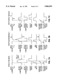
- FIG. 1 is a circuit diagram of a conventional infrared transmitter receiver pair.
- FIGS. 2A-C are waveform diagrams illustrating the effects of feedback in a conventional infrared receiver.
- FIGS. 3A-D are circuit diagrams illustrating conventional techniques for mitigating feedback.
- FIG. 4 is a circuit diagram of an embodiment of the present invention which utilizes positive feedback and first order bandwidth filtering.
- FIGS. 5A-C are waveform diagrams illustrating the behavior of the embodiment of the present invention shown in FIG. 4.
- FIG. 6 is a circuit diagram of an embodiment of the present invention which utilizes an output delay and isolates the AGC circuit from the feedback signal.
- FIGS. 7A-C are waveform diagrams illustrating the behavior of the embodiment of the present invention shown in FIG. 6.
- FIG. 8 is a circuit diagram of yet an embodiment of the present invention which also isolates the detect comparator from the feedback signal.
- FIG. 9 is a circuit diagram of an embodiment of the present invention which also isolates the bandwidth filter from the feedback signal.
- FIG. 10 is a circuit diagram of an embodiment of the present invention which monitors the receive signal path and controls the isolation signal responsive to the settling time of the feedback transient.
- FIG. 11 is a circuit diagram of an embodiment of the present invention which includes additional detail of the circuit design.
- FIG. 4 illustrates a circuit designed to mitigate the effects of feedback through control of the feedback phase with the design of the receiver bandwidth filter design.
- IrDA on-off modulation
- the receiver transient response has little overshoot, and either no AGC or high signal threshold AGC is used, then the positive feedback acts as dynamic hysteresis, producing an output pulse without any spurious transitions.
- the infrared receiver 420 of FIG. 4 is designed so that the feedback through parasitic capacitor 440 from D OUT to the photodiode input D IR is positive.
- a negative transition in the received signal at D IR results in a negative transition in the data output signal at D OUT which will, in turn, generate a corresponding negative spike in the feedback signal.
- FIG. 5B demonstrates the resulting waveforms when negative feedback is combined with the received signal at D IR .
- the received signal is countered by the much larger amplitude of the feedback spike which causes the signal at the input of detect comparator 442 to cross the detect threshold V DET repeatedly. This results in multiple transitions in data output signal thereby corrupting the data.
- the positive feedback reinforces the received signal, as demonstrated in FIG. 5C.
- the positive feedback when combined with the received signal at D IR , results in a signal at the input of comparator 442 that swings farther away from V DET responsive to the edges in D IR generating a single output pulse at D OUT .
- Bandpass filter 434 must be designed for good damped transient response to suppress signal ringing and overshoot.
- An example of a suitable filter is a Gaussian bandpass filter, which has roll-off edges in the signal output from the filter that have low ringing and overshoot transient response.
- the filter will temporally spread out the energy contained in the feedback spike. For example, a 20 nsec. spike is transformed into a 300 nsec. spike, which further contributes to the dynamic hysteresis discussed above.
- the AGC threshold V AGC of receiver 420 needs to be set above the peak feedback value by a margin adequate to prevent the peak feedback value from causing the gain to be adjusted downward by the AGC.
- AGC noise quieting which reduces signal interference from noise
- the output pulse width will vary more with signal level.
- AGC reduces the front end gain of amplifier 426 responsive to an increasing input signal on D IR .
- amplifier 426 will be highly sensitive because the AGC permits the gain to be high.
- the AGC will reduce the gain in response to the input signal including the noise level. This improves the noise immunity of the receiver 420.
- the receiver will function so long as the received signal strength is greater than the amplitude of the noise. From a practical standpoint, in a noisy environment, this permits the sending and receiving devices to be moved closer together to strengthen the received signal and the communications link will be able to function.
- the noise level will prevent the receiver from capturing the transmitted signal without corruption of the output data signal even when the transmitting device and receiver are close together because the noise signal will still have high enough amplitude to cause spurious output transitions in between valid output transitions.
- AGC improves the fidelity of the pulses in the data output D OUT .
- AGC reduces the effect of ringing, overshoot and undershoot when it reduces the sensitivity of amplifier 426.
- AGC improves the fidelity of the pulse by maintaining V DET at the center of the waveform.
- the amplitude of the positive feedback also causes the AGC to adjust the receiver sensitivity downward.
- the AGC reduces the gain in response to the positive feedback, the sensitivity of the receiver to the transmitted signal is also reduced and, particularly at high signal pulse rates, can cause the receiver to lose the input signal.
- the circuit of FIG. 4 is effective in reducing the effects of feedback, it still suffers from the effect of feedback transient overshoot or ringing, which, if it exceeds the detect level V DET , will cause undesirable extraneous output pulse transitions.
- V DET detect level
- filter design techniques can limit transient overshoot to a negligible level, in practice, reducing it to a value below 1/5 or 1/10 the peak level is difficult due to variable phase shift effects both within and outside the infrared receiver.
- Some of these variable phase shift effects are due to normal variances in parameters such as transmit pulse shape, photodiode time constant, photodiode capacitance, receiver output load capacitance, receiver supply voltage, and filter component values.
- receiver 420 can beneficially decrease the disruptive effects of feedback by 10 db-20 db for infrared receivers used with edge triggered, serial data communication controllers which do not need an accurate data pulse width or with receiver systems which do not require the benefits of a low threshold AGC.
- Infrared receiver 620 which is suitable for the use of low threshold AGC, adds delay 650 to the output signal from comparator 642, typically delaying the output by 1/2 of the pulse interval of the data signal to permit decay of the feedback pulse, as shown in FIG. 7A.
- Receiver 620 also includes a signal disable switch 648 controlled by AGC disable one-shot 652 which blocks the signal to the AGC input upon the leading edge of an output pulse transition on D OUT .
- AGC disable one-shot 652 By delaying the output signal, the peaks of the feedback signal from D OUT to D IR are shifted in time so that the feedback peak occurs toward the center of the pulse in the received signal at D IR .
- AGC disable one-shot 652 generates a signal disable pulse responsive to the falling edge in the output signal at D OUT which causes AGC disable switch 648 to open and isolate the input of AGC peak detector 636 from the received signal path for the duration of the signal disable pulse.
- the signal disable pulse must persist for a time interval sufficient for the feedback transient to settle below levels which would cause AGC gain reduction.
- AGC peak detector 636 is therefore isolated from the signal path at the time that the feedback pulse appears at the negative input to comparator 642. As a result, the gain control voltage stored in capacitor 628 during the disable period reflects the received signal strength and is not corrupted by the feedback signal.
- the AGC disable one-shot 652 may be replaced with an output edge triggered disable one shot which will generate a disable pulse responsive to both the falling and rising edges of the output signal at D OUT , as illustrated by the waveforms in FIG. 7C.
- An edge triggered disable will isolate the AGC peak detector 636 during feedback pulses for both the edges of the output pulse at D OUT .
- receiver 620 is substantially better than the performance of conventional receivers, it requires that receiver 620 be designed so that the feedback from D OUT to D IR is positive. Negative feedback will still cause spurious transitions in the output signal because the feedback is coupled to the input of comparator 642.
- Receiver 820 of FIG. 8 shows yet another embodiment of the present invention which is not dependent upon positive feedback.
- Signal disable switch 848 is positioned between the output of bandpass filter 834 and the inputs of both comparator 842 and AGC peak detector 836.
- Output edge triggered disable one-shot 852 receives the delayed output signal at D OUT and generates a disable pulse responsive to each of the falling and rising edges of the output signal.
- the disable signal must persist for a period long enough for the feedback transients to decay below a level that would cause spurious transitions in the output signal from comparator 842.
- the disable pulses cause signal disable switch 848 to isolate comparator 842 and AGC peak detector 836 from the received signal path during the times when the falling and rising feedback peaks are present at the output of bandpass filter 834.
- receiver 820 to obtain the improved AGC performance of receiver 620.
- receiver 820 is not dependent upon positive feedback because the input of comparator 842 is isolated from the feedback peaks, thereby preventing the negative feedback peaks from causing spurious transitions in the output signal at D OUT .
- FIG. 8 also shows greater detail of an example of an output edge triggered disable one-shot.
- One input terminal of exclusive-OR gate 852 receives the output signal directly while the other input terminal is coupled to the output signal through resistor 756 and to ground through capacitor 854.
- Resistor 856 and capacitor 854 further delay the output signal such that, when a pulse edge occurs in the output signal, the two inputs of XOR 852 will be at different values for a time period determined by the RC constant of resistor 856 and capacitor 854, which therefore also determine the width of the disable pulses generated by XOR 852.
- Receiver 920 in FIG. 9 is constructed with signal disable switch 948 interposed between the output of input amplifier 926 and bandpass filter 934. This configuration permits the disable pulses generated by XOR 952 responsive to the edges in the output signal to isolate bandpass filter 934, comparator 942 and AGC peak detector 936 from the receive signal path feedback from D OUT .
- This configuration causes the feedback transient to settle more rapidly because the transient is prevented from entering the bandpass filter 934 where the transient is prolonged due to the increase in ringing, overshoot and undershoot that would otherwise occur due to feedback transients in the output response of bandpass filter 934.
- This permits receiver 920 to tolerate larger amplitude feedback signals, use a narrower bandwidth to improve the signal to noise ratio of the receiver, or operate at faster pulse rates without corruption of the data output signal at D OUT .
- the duration of the disable pulses may be extended to account for variations in the settling time of the feedback peaks.
- faster communications formats such as the 4 Mb/s format described above, have narrow windows because the data is related to the temporal position of the pulse which requires rapid settling times. As a result, the disable signal generated by XOR 952 may not coincide exactly with the feedback peaks.
- the disable signal For example, if the disable signal is 1.5 us, then valid input signal transitions which have less than 1.5 us between them cannot be detected. To capture these signal transitions, it is necessary to set the disable signal duration to the minimum required to prevent feedback disruption. However, due to variances in IC timing circuit tolerances and variances in feedback due to variances in receiver packages and circuit board trace layout, it becomes necessary to set the signal disable period to a larger value than is typically required so as to ensure that most receivers will function without feedback disruption. This adds a difficult engineering burden of correctly determining the optimum signal disable duration and undesirable limiting maximum pulse rate on receiver packages or board layouts which have low feedback levels.
- receiver 1020 in FIG. 10 is designed with positive feedback and feedback detection which monitors the feedback transients and prevents signal disable switch 1048 from closing while a feedback transient is present.
- Feedback detect comparator 1060 compares the amplified input data signal at the output of input amplifier 1026 to the detection threshold voltage level V DET and outputs a high level signal so long as the amplified input signal is greater that the detection threshold.
- Exclusive-OR 1062 compares the output of the feedback detect comparator 1060 with the delayed digital output signal and outputs a high level signal if the two signals differ. Conversely, exclusive-OR 1062 outputs a low level if the two signals are in agreement. This low output signal will propagate through AND gate 1064 to close signal disable switch 1048 before the edge triggered disable signal output from exclusive-OR 1052 would normally cause switch 1048 to close. This permits receiver 1020 to operate at higher speeds when the transient settling time is faster than that predicted solely by the timing of the edge-triggered one shot circuit.
- the receiver 1120 of FIG. 11 illustrates the detailed circuit design for an embodiment of the present invention.
- the input amplifier stage for receiver 1120 is constructed from transistors 1178, 1180, 1182 and 1184.
- the gain control voltage accumulated on capacitor 1128 passes through gain control buffer 1176 and varies the amount of current shunted from voltage source V DD through transistors 1178 and 1182. If more current is shunted through transistors 1178 and 1182, then more of the current signal received at D IR is diverted through transistor 1182 and a correspondingly attenuated current signal passes through transistor 1184. Conversely, a lower gain control voltage will result in less current diverted through transistor 1182 and therefore more current is available for passage of a less attenuated received current signal through transistor 1184.
- the infrared current signal received at D IR from photodiode 24 modulates the current running through transistor 1184 to generate the voltage signal appearing at the negative input terminal of wideband transconductance amplifier 1174.
- the amplified received signal output from amplifier 1174 appears at the source terminals of pass gate transistors 1168 and 1170 which function as an isolation switch which is controlled by the isolation control signal generated at the output of NAND gate 1164.
- pass gate transistors 1168 and 1170 permit the received signal to pass through to AGC peak detector 1136, bandpass filter capacitor 1134 and comparator 1142 when the output from either XOR 1162 or XOR 1152 is low and otherwise isolates these components.
- the output of feedback detect comparator 1160 will go low once a feedback transient present at the output of amplifier 1174 has decayed below the analog reference voltage V AG (otherwise known as an analog ground), which is a stable voltage potential, typically at approximately the center of the range between V DD and the ground potential, which is used to bias the amplifiers of receiver 1120 at approximately the center of their operating range.
- V AG analog reference voltage
- DC and AC correction transconductance amplifier 1198 monitors V AG and shunts current from a regulated voltage source V REG to compensate for the DC and AC ambient currents produced by photodiode 24 and also to correct for bias offset errors of the components of receiver 1120.
- the digital data output signal generated by comparator 1142 in response to the input data signal received at D IR is delayed by the RC constant formed by resistors 1202 and capacitor 1204 as well as the gate delays introduced by inverters 1204 and 1206 in order to obtain the delayed digital output data signal which is presented at D out .
Abstract
Description
Claims (23)
Priority Applications (2)
| Application Number | Priority Date | Filing Date | Title |
|---|---|---|---|
| US08/827,402 US5864591A (en) | 1997-03-27 | 1997-03-27 | Apparatus and method for suppression of feedback in a communications receiver |
| US09/041,062 US6356375B1 (en) | 1997-03-27 | 1998-03-10 | Apparatus and method for an integrated photodiode in an infrared receiver |
Applications Claiming Priority (1)
| Application Number | Priority Date | Filing Date | Title |
|---|---|---|---|
| US08/827,402 US5864591A (en) | 1997-03-27 | 1997-03-27 | Apparatus and method for suppression of feedback in a communications receiver |
Related Child Applications (1)
| Application Number | Title | Priority Date | Filing Date |
|---|---|---|---|
| US09/041,062 Continuation US6356375B1 (en) | 1997-03-27 | 1998-03-10 | Apparatus and method for an integrated photodiode in an infrared receiver |
Publications (1)
| Publication Number | Publication Date |
|---|---|
| US5864591A true US5864591A (en) | 1999-01-26 |
Family
ID=25249127
Family Applications (2)
| Application Number | Title | Priority Date | Filing Date |
|---|---|---|---|
| US08/827,402 Expired - Lifetime US5864591A (en) | 1997-03-27 | 1997-03-27 | Apparatus and method for suppression of feedback in a communications receiver |
| US09/041,062 Expired - Lifetime US6356375B1 (en) | 1997-03-27 | 1998-03-10 | Apparatus and method for an integrated photodiode in an infrared receiver |
Family Applications After (1)
| Application Number | Title | Priority Date | Filing Date |
|---|---|---|---|
| US09/041,062 Expired - Lifetime US6356375B1 (en) | 1997-03-27 | 1998-03-10 | Apparatus and method for an integrated photodiode in an infrared receiver |
Country Status (1)
| Country | Link |
|---|---|
| US (2) | US5864591A (en) |
Cited By (32)
| Publication number | Priority date | Publication date | Assignee | Title |
|---|---|---|---|---|
| US6118829A (en) * | 1997-10-01 | 2000-09-12 | Integration Associates, Inc. | Apparatus and method for automatic mode selection in a communications receiver |
| EP1093093A2 (en) * | 1999-10-08 | 2001-04-18 | Crane Co. | Vending machine communication interference shield |
| US6240283B1 (en) * | 1997-08-07 | 2001-05-29 | Integration Associates, Inc. | Apparatus and method for feedback mitigation in a low speed communications receiver |
| US6243183B1 (en) * | 1996-03-25 | 2001-06-05 | Telefonaktiebolaget Lm Ericsson (Publ) | Method and equipment for optical communication |
| US6249552B1 (en) * | 1997-09-29 | 2001-06-19 | Nortel Networks Limited | Audio frequency recovery—DC restorer circuit for cordless phone applications |
| US6356375B1 (en) * | 1997-03-27 | 2002-03-12 | Integration Associates, Inc. | Apparatus and method for an integrated photodiode in an infrared receiver |
| US6359517B1 (en) | 2000-01-28 | 2002-03-19 | Integration Associates Incorporated | Photodiode transimpedance circuit |
| US6449078B1 (en) * | 1997-08-05 | 2002-09-10 | Matsushita Electric Industrial Co., Ltd. | Optical receiver, method for optical transmission in space, optical transmitting in space apparatus and method for optical transmission |
| US6556330B2 (en) * | 1998-03-10 | 2003-04-29 | Integration Associates, Inc. | Apparatus and method for an integrated photodiode in an infrared receiver |
| US20040022334A1 (en) * | 2002-08-01 | 2004-02-05 | Philipp Roosli | Digital iterative gain control |
| US6836549B1 (en) * | 1998-09-02 | 2004-12-28 | Macrovision Corporation | Method and apparatus for synthesizing and reducing the effects of video copy protection signals |
| EP1500216A1 (en) * | 2002-04-18 | 2005-01-26 | Dorsal Networks, Inc. | Systems and methods for compensating for signal transients |
| US20050123307A1 (en) * | 2003-12-09 | 2005-06-09 | Rohm Company, Ltd. | Optical receiver and data communication apparatus comprising same |
| US20050185704A1 (en) * | 2002-08-22 | 2005-08-25 | Infineon Technologies Ag | Method and circuit for controlling the input signal for a contactless transponder |
| US20060060955A1 (en) * | 2004-09-22 | 2006-03-23 | Texas Instruments Incorporated | Stacked die infrared transceiver bus |
| US7053674B1 (en) * | 2004-12-13 | 2006-05-30 | Allegro Microsystems, Inc. | Track-and-hold peak detector circuit |
| US20060184975A1 (en) * | 2005-02-16 | 2006-08-17 | Qwest Communications International Inc. | Wireless digital video recorder |
| US20060184983A1 (en) * | 2005-02-16 | 2006-08-17 | Qwest Communications International Inc. | Wireless digital video recorder manager |
| US20060210064A1 (en) * | 2004-12-03 | 2006-09-21 | Integration Associates Inc. | Ring detection and snoop circuit |
| US20060218598A1 (en) * | 2005-02-16 | 2006-09-28 | Qwest Communications International Inc. | Wireless digital video recorders - content sharing systems and methods |
| US20060251429A1 (en) * | 2005-05-06 | 2006-11-09 | Heqing Yi | Burst optical receiver with AC coupling and integrator feedback network |
| DE10157224B4 (en) * | 2000-12-04 | 2008-09-18 | Samsung Electronics Co., Ltd., Suwon | Parameter monitoring device for a high voltage chamber in a semiconductor wafer processing system |
| US7486386B1 (en) | 2007-09-21 | 2009-02-03 | Silison Laboratories Inc. | Optical reflectance proximity sensor |
| US20100021176A1 (en) * | 2006-11-16 | 2010-01-28 | Integration Associates Inc. | Apparatus and Method for Near-Field Communication |
| ITBO20110452A1 (en) * | 2011-07-28 | 2011-10-27 | Marposs Spa | SYSTEM AND METHOD TO CHECK POSITION AND / OR DIMENSIONS OF MECHANICAL PARTS |
| CN102355215A (en) * | 2011-05-20 | 2012-02-15 | 武汉艾立卡电子有限公司 | Non-contact audio equipment volume controller and control method thereof |
| US20120294455A1 (en) * | 2011-05-20 | 2012-11-22 | Yamaha Corporation | Speaker apparatus |
| US8384559B2 (en) | 2010-04-13 | 2013-02-26 | Silicon Laboratories Inc. | Sensor device with flexible interface and updatable information store |
| US20130214135A1 (en) * | 2012-02-16 | 2013-08-22 | International Business Machines Corporation | Optical receiver using infinite impulse response decision feedback equalization |
| US9608681B1 (en) * | 2015-09-29 | 2017-03-28 | Silicon Laboratories Inc. | Output driver architecture with low spur noise |
| US20170244493A1 (en) * | 2014-09-16 | 2017-08-24 | Cosemi Technologies Inc. | Method for improving signal quality of a digital signal being processed in a linear device and apparatus using the same |
| US9820141B2 (en) * | 2016-03-14 | 2017-11-14 | Stmicroelectronics S.R.L. | Receiver and corresponding process |
Families Citing this family (8)
| Publication number | Priority date | Publication date | Assignee | Title |
|---|---|---|---|---|
| US6915083B1 (en) * | 1998-12-15 | 2005-07-05 | Zilog, Inc. | Signal receiver having wide band amplification capability |
| AU6729100A (en) * | 1999-08-25 | 2001-03-19 | Hamamatsu Photonics K.K. | Optical receiver and method of support and arrangement thereof |
| DE10047380B4 (en) * | 2000-09-25 | 2007-05-10 | Siemens Ag | Method for controlling the working range of a modulator and associated drive unit |
| US7820030B2 (en) * | 2003-04-16 | 2010-10-26 | Handylab, Inc. | System and method for electrochemical detection of biological compounds |
| KR100752523B1 (en) * | 2005-12-15 | 2007-08-29 | 주식회사 에이디텍 | An infrared-ray receiver |
| DE102008029620A1 (en) * | 2008-06-23 | 2009-12-24 | Vishay Semiconductor Gmbh | Infrared receiver circuit |
| CN102684778B (en) * | 2012-04-23 | 2015-01-21 | 泉芯电子技术(深圳)有限公司 | Infrared receiver and method for improving frequency response of input end of infrared receiver |
| CN111033189B (en) * | 2017-07-03 | 2021-12-31 | 马尔苏普拉控股公司 | Light-based communication system |
Citations (8)
| Publication number | Priority date | Publication date | Assignee | Title |
|---|---|---|---|---|
| US4241455A (en) * | 1977-12-29 | 1980-12-23 | Sperry Corporation | Data receiving and processing circuit |
| US4528519A (en) * | 1983-01-12 | 1985-07-09 | Ncr Corporation | Automatic gain control |
| US4757502A (en) * | 1985-01-22 | 1988-07-12 | Alcatel Thomson Faisceaux Hertizens | Automatic gain control method and circuit for a time division multiple access receiver |
| US5081653A (en) * | 1987-08-18 | 1992-01-14 | Nec Corporation | Automatic gain control circuit for multilevel duobinary AM/PSK modulated signals |
| US5329115A (en) * | 1993-04-29 | 1994-07-12 | International Business Machines Corporation | Optical receiver circuit |
| US5361395A (en) * | 1991-02-28 | 1994-11-01 | Kabushiki Kaisha Toshiba | Gain control circuit |
| US5557634A (en) * | 1994-10-14 | 1996-09-17 | International Business Machines Corporation | Multiprotocol directed infrared communication controller |
| US5760942A (en) * | 1994-04-07 | 1998-06-02 | Photonics Corporation | Noise tolerant receiver for wideband optical transmission system |
Family Cites Families (8)
| Publication number | Priority date | Publication date | Assignee | Title |
|---|---|---|---|---|
| US3619660A (en) | 1970-04-14 | 1971-11-09 | Bell Telephone Labor Inc | Automatic gain control utilizing controlled sampling |
| JP3161910B2 (en) | 1994-07-26 | 2001-04-25 | シャープ株式会社 | Communication device |
| FI97659C (en) | 1995-01-13 | 1997-01-27 | Nokia Mobile Phones Ltd | Method and apparatus for saving power during infrared data transmission |
| JPH09181632A (en) | 1995-12-22 | 1997-07-11 | Alps Electric Co Ltd | Delayed automatic gain control circuit |
| JP3350376B2 (en) | 1996-11-25 | 2002-11-25 | シャープ株式会社 | Waveform shaping circuit and infrared data communication device using the same |
| US6018650A (en) | 1996-12-18 | 2000-01-25 | Aironet Wireless Communications, Inc. | Cellular communication devices with automated power level adjust |
| US5917865A (en) | 1996-12-31 | 1999-06-29 | Lucent Technologies, Inc. | Digital automatic gain control employing two-stage gain-determination process |
| US5864591A (en) * | 1997-03-27 | 1999-01-26 | Integration Associates, Inc. | Apparatus and method for suppression of feedback in a communications receiver |
-
1997
- 1997-03-27 US US08/827,402 patent/US5864591A/en not_active Expired - Lifetime
-
1998
- 1998-03-10 US US09/041,062 patent/US6356375B1/en not_active Expired - Lifetime
Patent Citations (8)
| Publication number | Priority date | Publication date | Assignee | Title |
|---|---|---|---|---|
| US4241455A (en) * | 1977-12-29 | 1980-12-23 | Sperry Corporation | Data receiving and processing circuit |
| US4528519A (en) * | 1983-01-12 | 1985-07-09 | Ncr Corporation | Automatic gain control |
| US4757502A (en) * | 1985-01-22 | 1988-07-12 | Alcatel Thomson Faisceaux Hertizens | Automatic gain control method and circuit for a time division multiple access receiver |
| US5081653A (en) * | 1987-08-18 | 1992-01-14 | Nec Corporation | Automatic gain control circuit for multilevel duobinary AM/PSK modulated signals |
| US5361395A (en) * | 1991-02-28 | 1994-11-01 | Kabushiki Kaisha Toshiba | Gain control circuit |
| US5329115A (en) * | 1993-04-29 | 1994-07-12 | International Business Machines Corporation | Optical receiver circuit |
| US5760942A (en) * | 1994-04-07 | 1998-06-02 | Photonics Corporation | Noise tolerant receiver for wideband optical transmission system |
| US5557634A (en) * | 1994-10-14 | 1996-09-17 | International Business Machines Corporation | Multiprotocol directed infrared communication controller |
Non-Patent Citations (14)
| Title |
|---|
| Dr. Keming W. Yeh and Dr. Lichen Wang "An Introduction to the IrDA Standard and System Implementaiton" Wireless System Design May 1996, 11 pages. |
| Dr. Keming W. Yeh and Dr. Lichen Wang An Introduction to the IrDA Standard and System Implementaiton Wireless System Design May 1996, 11 pages. * |
| Ernesto Perea "Technology Directions; Optical Interconnects, High Temperature, & Packaging" Feb. 10, 1996, ISSCC96, 8 pages. |
| Ernesto Perea Technology Directions; Optical Interconnects, High Temperature, & Packaging Feb. 10, 1996, ISSCC96, 8 pages. * |
| Hewlett Packard Infrared Transceiver Preliminary Technical Data HSDL 1100 Nov. 17, 1995. * |
| Hewlett-Packard "Infrared Transceiver Preliminary Technical Data HSDL-1100" Nov. 17, 1995. |
| IBM Microelectronics "Infrared Transceiver Module--IBM31T1101" Nov. 6, 1996, http:///www.chips.ibm.com. |
| IBM Microelectronics Infrared Transceiver Module IBM31T1101 Nov. 6, 1996, http:///www.chips.ibm.com. * |
| Novalog, Inc. "SIRFIR™ 4Mbps IrDA Transceiver" Apr. 1996 info@novalog.com. |
| Novalog, Inc. SIRFIR 4Mbps IrDA Transceiver Apr. 1996 info novalog.com. * |
| Temic Semiconductors "IrDA Compatible Data Transmission" Apr. 1996, pp. 1-18. |
| Temic Semiconductors "TFDS 6000 Integrated Infrared Transceiver Module IrDA" Aug. 1996, 12 pages. |
| Temic Semiconductors IrDA Compatible Data Transmission Apr. 1996, pp. 1 18. * |
| Temic Semiconductors TFDS 6000 Integrated Infrared Transceiver Module IrDA Aug. 1996, 12 pages. * |
Cited By (54)
| Publication number | Priority date | Publication date | Assignee | Title |
|---|---|---|---|---|
| US6243183B1 (en) * | 1996-03-25 | 2001-06-05 | Telefonaktiebolaget Lm Ericsson (Publ) | Method and equipment for optical communication |
| US6356375B1 (en) * | 1997-03-27 | 2002-03-12 | Integration Associates, Inc. | Apparatus and method for an integrated photodiode in an infrared receiver |
| US6449078B1 (en) * | 1997-08-05 | 2002-09-10 | Matsushita Electric Industrial Co., Ltd. | Optical receiver, method for optical transmission in space, optical transmitting in space apparatus and method for optical transmission |
| US6240283B1 (en) * | 1997-08-07 | 2001-05-29 | Integration Associates, Inc. | Apparatus and method for feedback mitigation in a low speed communications receiver |
| US6249552B1 (en) * | 1997-09-29 | 2001-06-19 | Nortel Networks Limited | Audio frequency recovery—DC restorer circuit for cordless phone applications |
| US6118829A (en) * | 1997-10-01 | 2000-09-12 | Integration Associates, Inc. | Apparatus and method for automatic mode selection in a communications receiver |
| US6556330B2 (en) * | 1998-03-10 | 2003-04-29 | Integration Associates, Inc. | Apparatus and method for an integrated photodiode in an infrared receiver |
| US8094818B2 (en) | 1998-09-02 | 2012-01-10 | Rovi Solutions Corporation | Method to synthesize video copy protection signals |
| US6836549B1 (en) * | 1998-09-02 | 2004-12-28 | Macrovision Corporation | Method and apparatus for synthesizing and reducing the effects of video copy protection signals |
| US20050117749A1 (en) * | 1998-09-02 | 2005-06-02 | Ronald Quan | Method and apparatus to synthesize and defeat video copy protection signals |
| EP1093093A3 (en) * | 1999-10-08 | 2002-08-28 | Crane Co. | Vending machine communication interference shield |
| EP1093093A2 (en) * | 1999-10-08 | 2001-04-18 | Crane Co. | Vending machine communication interference shield |
| US6359517B1 (en) | 2000-01-28 | 2002-03-19 | Integration Associates Incorporated | Photodiode transimpedance circuit |
| DE10157224B4 (en) * | 2000-12-04 | 2008-09-18 | Samsung Electronics Co., Ltd., Suwon | Parameter monitoring device for a high voltage chamber in a semiconductor wafer processing system |
| EP1500216A4 (en) * | 2002-04-18 | 2006-12-06 | Dorsal Networks Inc | Systems and methods for compensating for signal transients |
| EP1500216A1 (en) * | 2002-04-18 | 2005-01-26 | Dorsal Networks, Inc. | Systems and methods for compensating for signal transients |
| US20040022334A1 (en) * | 2002-08-01 | 2004-02-05 | Philipp Roosli | Digital iterative gain control |
| US7822349B2 (en) * | 2002-08-01 | 2010-10-26 | Inncom International, Inc. | Digital iterative gain control |
| US7545892B2 (en) * | 2002-08-22 | 2009-06-09 | Infineon Technologies Ag | Method and circuit for controlling the input signal for a contactless transponder |
| US20050185704A1 (en) * | 2002-08-22 | 2005-08-25 | Infineon Technologies Ag | Method and circuit for controlling the input signal for a contactless transponder |
| US7509059B2 (en) * | 2003-12-09 | 2009-03-24 | Rohm Co., Ltd. | Optical receiver and data communication apparatus comprising same |
| US20050123307A1 (en) * | 2003-12-09 | 2005-06-09 | Rohm Company, Ltd. | Optical receiver and data communication apparatus comprising same |
| US20080094082A1 (en) * | 2004-09-22 | 2008-04-24 | Texas Instruments Incorporated | Die Infrared Transceiver Bus |
| US20060060955A1 (en) * | 2004-09-22 | 2006-03-23 | Texas Instruments Incorporated | Stacked die infrared transceiver bus |
| US7536005B2 (en) * | 2004-12-03 | 2009-05-19 | Silicon Laboratories, Inc. | Ring detection and snoop circuit |
| US20060210064A1 (en) * | 2004-12-03 | 2006-09-21 | Integration Associates Inc. | Ring detection and snoop circuit |
| US7053674B1 (en) * | 2004-12-13 | 2006-05-30 | Allegro Microsystems, Inc. | Track-and-hold peak detector circuit |
| US20060125530A1 (en) * | 2004-12-13 | 2006-06-15 | Romero Hernan D | Track-and-hold peak detector circuit |
| US8590000B2 (en) | 2005-02-16 | 2013-11-19 | Qwest Communications International Inc. | Wireless digital video recorder |
| US20060184975A1 (en) * | 2005-02-16 | 2006-08-17 | Qwest Communications International Inc. | Wireless digital video recorder |
| US8613037B2 (en) | 2005-02-16 | 2013-12-17 | Qwest Communications International Inc. | Wireless digital video recorder manager |
| US8407746B2 (en) * | 2005-02-16 | 2013-03-26 | Qwest Communications International Inc. | Wireless digital video recorders—content sharing systems and methods |
| US20060218598A1 (en) * | 2005-02-16 | 2006-09-28 | Qwest Communications International Inc. | Wireless digital video recorders - content sharing systems and methods |
| US20060184983A1 (en) * | 2005-02-16 | 2006-08-17 | Qwest Communications International Inc. | Wireless digital video recorder manager |
| US7599631B2 (en) * | 2005-05-06 | 2009-10-06 | Yi Heqing | Burst optical receiver with AC coupling and integrator feedback network |
| US20060251429A1 (en) * | 2005-05-06 | 2006-11-09 | Heqing Yi | Burst optical receiver with AC coupling and integrator feedback network |
| US8041227B2 (en) | 2006-11-16 | 2011-10-18 | Silicon Laboratories Inc. | Apparatus and method for near-field communication |
| US20100021176A1 (en) * | 2006-11-16 | 2010-01-28 | Integration Associates Inc. | Apparatus and Method for Near-Field Communication |
| US7486386B1 (en) | 2007-09-21 | 2009-02-03 | Silison Laboratories Inc. | Optical reflectance proximity sensor |
| US8384559B2 (en) | 2010-04-13 | 2013-02-26 | Silicon Laboratories Inc. | Sensor device with flexible interface and updatable information store |
| CN102355215A (en) * | 2011-05-20 | 2012-02-15 | 武汉艾立卡电子有限公司 | Non-contact audio equipment volume controller and control method thereof |
| US20120294455A1 (en) * | 2011-05-20 | 2012-11-22 | Yamaha Corporation | Speaker apparatus |
| US9357303B2 (en) * | 2011-05-20 | 2016-05-31 | Yamaha Corporation | Speaker apparatus |
| CN102355215B (en) * | 2011-05-20 | 2013-10-02 | 武汉艾立卡电子有限公司 | Non-contact audio equipment volume controller and control method thereof |
| ITBO20110452A1 (en) * | 2011-07-28 | 2011-10-27 | Marposs Spa | SYSTEM AND METHOD TO CHECK POSITION AND / OR DIMENSIONS OF MECHANICAL PARTS |
| US20130214135A1 (en) * | 2012-02-16 | 2013-08-22 | International Business Machines Corporation | Optical receiver using infinite impulse response decision feedback equalization |
| US8798484B2 (en) * | 2012-02-16 | 2014-08-05 | International Business Machines Corporation | Optical receiver using infinite impulse response decision feedback equalization |
| US8977138B2 (en) * | 2012-02-16 | 2015-03-10 | International Business Machines Corporation | Optical receiver using infinite impulse response decision feedback equalization |
| US20130216241A1 (en) * | 2012-02-16 | 2013-08-22 | International Business Machines Corporation | Optical receiver using infinite impulse response decision feedback equalization |
| US20170244493A1 (en) * | 2014-09-16 | 2017-08-24 | Cosemi Technologies Inc. | Method for improving signal quality of a digital signal being processed in a linear device and apparatus using the same |
| US9608681B1 (en) * | 2015-09-29 | 2017-03-28 | Silicon Laboratories Inc. | Output driver architecture with low spur noise |
| US9820141B2 (en) * | 2016-03-14 | 2017-11-14 | Stmicroelectronics S.R.L. | Receiver and corresponding process |
| US20180035283A1 (en) * | 2016-03-14 | 2018-02-01 | Stmicroelectronics S.R.L. | Receiver and corresponding process |
| US10237725B2 (en) * | 2016-03-14 | 2019-03-19 | Stmicroelectronics S.R.L. | Receiver and corresponding process |
Also Published As
| Publication number | Publication date |
|---|---|
| US6356375B1 (en) | 2002-03-12 |
Similar Documents
| Publication | Publication Date | Title |
|---|---|---|
| US5864591A (en) | Apparatus and method for suppression of feedback in a communications receiver | |
| US6081558A (en) | Apparatus and method for low power operation with high sensitivity in a communications receiver | |
| US6169765B1 (en) | Apparatus and method for output signal pulse width error correction in a communications receiver | |
| US6556330B2 (en) | Apparatus and method for an integrated photodiode in an infrared receiver | |
| US4498001A (en) | Transimpedance amplifier for optical receivers | |
| US6240283B1 (en) | Apparatus and method for feedback mitigation in a low speed communications receiver | |
| US6242732B1 (en) | Optical receiver with a control loop providing wide dynamic range | |
| JP2005533379A (en) | Method and apparatus for directly modulating a laser diode using a multistage laser driver circuit | |
| US6118829A (en) | Apparatus and method for automatic mode selection in a communications receiver | |
| US6198118B1 (en) | Distributed photodiode structure | |
| US10432305B2 (en) | Loss of signal detector | |
| US5790295A (en) | Gated integrator preamplifier for infrared data networks | |
| GB2293931A (en) | Adaptive decision threshold setting circuit | |
| JP2003152649A (en) | Optical receiver | |
| US5386109A (en) | Pre-amplifier for optical receiving and optical receiver using the same | |
| US4543664A (en) | Direct current coupled data transmission | |
| US5373388A (en) | AC coupled fiber optic receiver with DC coupled characteristics | |
| KR100322520B1 (en) | Infrared receiver | |
| WO2017074385A1 (en) | Receivers with automatic gain control | |
| US5684831A (en) | Data bus with noise immunity | |
| US7126412B2 (en) | Preamplification circuit | |
| US6166669A (en) | Protection from inbound signal noise caused by inductively coupled outbound signal transitions by controlling decision threshold | |
| JP3402674B2 (en) | Optical receiving preamplifier and optical receiving apparatus | |
| WO2012017691A1 (en) | Ac coupled single-ended lvds receiving circuit comprising low-pass filter and voltage regulator | |
| US11881827B2 (en) | Traveling-wave transimpedance amplifier |
Legal Events
| Date | Code | Title | Description |
|---|---|---|---|
| AS | Assignment |
Owner name: INTEGRATION ASSOCIATES, INC., CALIFORNIA Free format text: ASSIGNMENT OF ASSIGNORS INTEREST;ASSIGNOR:HOLCOMBE, WAYNE T.;REEL/FRAME:008498/0239 Effective date: 19970326 |
|
| FPAY | Fee payment |
Year of fee payment: 4 |
|
| REMI | Maintenance fee reminder mailed | ||
| REMI | Maintenance fee reminder mailed | ||
| REIN | Reinstatement after maintenance fee payment confirmed | ||
| FP | Lapsed due to failure to pay maintenance fee |
Effective date: 20070126 |
|
| FEPP | Fee payment procedure |
Free format text: PETITION RELATED TO MAINTENANCE FEES GRANTED (ORIGINAL EVENT CODE: PMFG); ENTITY STATUS OF PATENT OWNER: LARGE ENTITY Free format text: PETITION RELATED TO MAINTENANCE FEES FILED (ORIGINAL EVENT CODE: PMFP); ENTITY STATUS OF PATENT OWNER: LARGE ENTITY |
|
| AS | Assignment |
Owner name: SILICON LABS INTEGRATION, INC., CALIFORNIA Free format text: CHANGE OF NAME;ASSIGNOR:INTEGRATION ASSOCIATES INCORPORATED;REEL/FRAME:021658/0295 Effective date: 20080729 Owner name: SILICON LABS INTEGRATION, INC.,CALIFORNIA Free format text: CHANGE OF NAME;ASSIGNOR:INTEGRATION ASSOCIATES INCORPORATED;REEL/FRAME:021658/0295 Effective date: 20080729 |
|
| PRDP | Patent reinstated due to the acceptance of a late maintenance fee |
Effective date: 20081031 |
|
| AS | Assignment |
Owner name: SILICON LABORATORIES INC., TEXAS Free format text: ASSIGNMENT OF ASSIGNORS INTEREST;ASSIGNOR:SILIBON LABS INTEGRATION, INC.;REEL/FRAME:021785/0958 Effective date: 20081024 Owner name: SILICON LABORATORIES INC.,TEXAS Free format text: ASSIGNMENT OF ASSIGNORS INTEREST;ASSIGNOR:SILIBON LABS INTEGRATION, INC.;REEL/FRAME:021785/0958 Effective date: 20081024 |
|
| FPAY | Fee payment |
Year of fee payment: 8 |
|
| STCF | Information on status: patent grant |
Free format text: PATENTED CASE |
|
| SULP | Surcharge for late payment | ||
| FEPP | Fee payment procedure |
Free format text: PAYOR NUMBER ASSIGNED (ORIGINAL EVENT CODE: ASPN); ENTITY STATUS OF PATENT OWNER: LARGE ENTITY Free format text: PAYER NUMBER DE-ASSIGNED (ORIGINAL EVENT CODE: RMPN); ENTITY STATUS OF PATENT OWNER: LARGE ENTITY |
|
| FPAY | Fee payment |
Year of fee payment: 12 |