US5867537A - Balanced tranversal I,Q filters for quadrature modulators - Google Patents
Balanced tranversal I,Q filters for quadrature modulators Download PDFInfo
- Publication number
- US5867537A US5867537A US08/937,248 US93724897A US5867537A US 5867537 A US5867537 A US 5867537A US 93724897 A US93724897 A US 93724897A US 5867537 A US5867537 A US 5867537A
- Authority
- US
- United States
- Prior art keywords
- signal
- output
- balanced
- outputs
- output signals
- Prior art date
- Legal status (The legal status is an assumption and is not a legal conclusion. Google has not performed a legal analysis and makes no representation as to the accuracy of the status listed.)
- Expired - Lifetime
Links
Images


Classifications
-
- H—ELECTRICITY
- H04—ELECTRIC COMMUNICATION TECHNIQUE
- H04B—TRANSMISSION
- H04B1/00—Details of transmission systems, not covered by a single one of groups H04B3/00 - H04B13/00; Details of transmission systems not characterised by the medium used for transmission
- H04B1/0003—Software-defined radio [SDR] systems, i.e. systems wherein components typically implemented in hardware, e.g. filters or modulators/demodulators, are implented using software, e.g. by involving an AD or DA conversion stage such that at least part of the signal processing is performed in the digital domain
- H04B1/0007—Software-defined radio [SDR] systems, i.e. systems wherein components typically implemented in hardware, e.g. filters or modulators/demodulators, are implented using software, e.g. by involving an AD or DA conversion stage such that at least part of the signal processing is performed in the digital domain wherein the AD/DA conversion occurs at radiofrequency or intermediate frequency stage
- H04B1/0014—Software-defined radio [SDR] systems, i.e. systems wherein components typically implemented in hardware, e.g. filters or modulators/demodulators, are implented using software, e.g. by involving an AD or DA conversion stage such that at least part of the signal processing is performed in the digital domain wherein the AD/DA conversion occurs at radiofrequency or intermediate frequency stage using DSP [Digital Signal Processor] quadrature modulation and demodulation
-
- H—ELECTRICITY
- H04—ELECTRIC COMMUNICATION TECHNIQUE
- H04B—TRANSMISSION
- H04B1/00—Details of transmission systems, not covered by a single one of groups H04B3/00 - H04B13/00; Details of transmission systems not characterised by the medium used for transmission
- H04B1/0003—Software-defined radio [SDR] systems, i.e. systems wherein components typically implemented in hardware, e.g. filters or modulators/demodulators, are implented using software, e.g. by involving an AD or DA conversion stage such that at least part of the signal processing is performed in the digital domain
- H04B1/0028—Software-defined radio [SDR] systems, i.e. systems wherein components typically implemented in hardware, e.g. filters or modulators/demodulators, are implented using software, e.g. by involving an AD or DA conversion stage such that at least part of the signal processing is performed in the digital domain wherein the AD/DA conversion occurs at baseband stage
- H04B1/0039—Software-defined radio [SDR] systems, i.e. systems wherein components typically implemented in hardware, e.g. filters or modulators/demodulators, are implented using software, e.g. by involving an AD or DA conversion stage such that at least part of the signal processing is performed in the digital domain wherein the AD/DA conversion occurs at baseband stage using DSP [Digital Signal Processor] quadrature modulation and demodulation
-
- H—ELECTRICITY
- H04—ELECTRIC COMMUNICATION TECHNIQUE
- H04B—TRANSMISSION
- H04B1/00—Details of transmission systems, not covered by a single one of groups H04B3/00 - H04B13/00; Details of transmission systems not characterised by the medium used for transmission
- H04B1/38—Transceivers, i.e. devices in which transmitter and receiver form a structural unit and in which at least one part is used for functions of transmitting and receiving
- H04B1/40—Circuits
-
- H—ELECTRICITY
- H04—ELECTRIC COMMUNICATION TECHNIQUE
- H04L—TRANSMISSION OF DIGITAL INFORMATION, e.g. TELEGRAPHIC COMMUNICATION
- H04L25/00—Baseband systems
- H04L25/02—Details ; arrangements for supplying electrical power along data transmission lines
- H04L25/03—Shaping networks in transmitter or receiver, e.g. adaptive shaping networks
- H04L25/03828—Arrangements for spectral shaping; Arrangements for providing signals with specified spectral properties
- H04L25/03834—Arrangements for spectral shaping; Arrangements for providing signals with specified spectral properties using pulse shaping
-
- H—ELECTRICITY
- H04—ELECTRIC COMMUNICATION TECHNIQUE
- H04L—TRANSMISSION OF DIGITAL INFORMATION, e.g. TELEGRAPHIC COMMUNICATION
- H04L27/00—Modulated-carrier systems
- H04L27/18—Phase-modulated carrier systems, i.e. using phase-shift keying
- H04L27/20—Modulator circuits; Transmitter circuits
- H04L27/2003—Modulator circuits; Transmitter circuits for continuous phase modulation
- H04L27/2007—Modulator circuits; Transmitter circuits for continuous phase modulation in which the phase change within each symbol period is constrained
- H04L27/2017—Modulator circuits; Transmitter circuits for continuous phase modulation in which the phase change within each symbol period is constrained in which the phase changes are non-linear, e.g. generalized and Gaussian minimum shift keying, tamed frequency modulation
-
- H—ELECTRICITY
- H04—ELECTRIC COMMUNICATION TECHNIQUE
- H04L—TRANSMISSION OF DIGITAL INFORMATION, e.g. TELEGRAPHIC COMMUNICATION
- H04L27/00—Modulated-carrier systems
- H04L27/18—Phase-modulated carrier systems, i.e. using phase-shift keying
- H04L27/20—Modulator circuits; Transmitter circuits
- H04L27/2032—Modulator circuits; Transmitter circuits for discrete phase modulation, e.g. in which the phase of the carrier is modulated in a nominally instantaneous manner
- H04L27/2053—Modulator circuits; Transmitter circuits for discrete phase modulation, e.g. in which the phase of the carrier is modulated in a nominally instantaneous manner using more than one carrier, e.g. carriers with different phases
- H04L27/206—Modulator circuits; Transmitter circuits for discrete phase modulation, e.g. in which the phase of the carrier is modulated in a nominally instantaneous manner using more than one carrier, e.g. carriers with different phases using a pair of orthogonal carriers, e.g. quadrature carriers
- H04L27/2064—Modulator circuits; Transmitter circuits for discrete phase modulation, e.g. in which the phase of the carrier is modulated in a nominally instantaneous manner using more than one carrier, e.g. carriers with different phases using a pair of orthogonal carriers, e.g. quadrature carriers using microwave technology
Definitions
- the invention relates to methods and apparatuses for the realization of spectral containment of radio transmissions so that they do not cause adjacent channel interference and, in particular, for the realization of spectral containment of high bitrate digital transmissions such as TDMA or CDMA cellular telephone signals.
- the GSM TDMA system codes speech using convolutional coding and transmits the coded speech using one or two out of 16 timeslots depending on whether a half-rate or a full-rate channel is allocated.
- An IS-54 system also convolutionally codes speech and then transmits it using one or two out of six timeslots.
- An IS-95 system uses convolutional coding plus bit repetition and transmits the speech using 2, 4, 8 or 16 out of 16 timeslots depending on whether the speech sound is a voiced sound, non-voiced sound or silence/background noise. In all cases therefore, the bitrate of speech is first compressed to remove natural redundance and then the bitrate is increased by using intelligent coding to obtain a higher bitrate stream for transmission that is more tolerant of interference.
- a transmitter for such digitally coded signals preferably comprises a balanced quadrature modulator.
- FIG. 1 illustrates a prior art arrangement of a quadrature modulator for synthesizing an arbitrarily modulated signal.
- a digital signal processor (DSP) 30 calculates time-spaced samples of the real and imaginary parts of a desired complex modulation. The real part is given by the desired amplitude times the cosine of the desired phase angle, while the imaginary part is given by the amplitude times the sine of the phase angle. In this way both Amplitude Modulated (AM) signals or Phase Modulated (PM) signals can be generated, or signals comprising both, the result of which is generally known as complex modulated signals.
- AM Amplitude Modulated
- PM Phase Modulated
- the numerical samples calculated by the DSP 30 are transferred to a pair of Digital-to-Analog (D-to-A) convertors 31 that convert each numerical sample pair into a pair of analog voltages known as I (In-phase) and Q (Quadrature) signals.
- D-to-A Digital-to-Analog
- a sequence of such numerical samples generates I and Q waveforms but in a stepwise fashion.
- I and Q smoothing filters 32 are necessary. These are low-pass filters that pass all modulation spectral components of interest but suppress the higher frequency components of the spectrum associated with the stepwise or piecewise linear I,Q waveforms from the D-to-A convertors 31.
- the smoothed I,Q waveforms are applied to a pair of balanced modulators 33 together with cosine and sine carrier frequency signals, this arrangement being known as a quadrature modulator.
- This arrangement described so far and illustrated in FIG. 1 belongs to the well-known prior art.
- the DSP 30 produces numerical I and Q waveforms representative of the desired digital or analog modulation and then D-to-A convertors 31 convert the numerical I,Q representations to analog I,Q modulating waveforms.
- Filters 32 remove discontinuities due to the finite time sampling and quantization of the numerical I,Q signals to produce continuous I,Q waveforms, thus avoiding spectral splatter into adjacent radio channels.
- the smoothed I,Q waveforms are applied to sine and cosine radio frequency-carriers using quadrature modulator 33.
- the two balanced modulators are accurately matched, (2) the levels of the I and Q signals are accurately controlled relative to each other, and (3) the balanced modulators have low carrier leakage or offset, that is, the output signal of a balanced modulator should be zero when its respective I or Q modulating signal is zero.
- the zero point of an I or Q waveform cannot be defined to be zero voltage, but must be defined to be some positive reference voltage such as half the supply voltage. Then when an I or Q waveform swings below this reference voltage it will be interpreted as negative, and positive when it swings above.
- the numerical I and Q signals from DSP 30 are transferred to a delta-sigma ( ⁇ - ⁇ ) convertor 41.
- This device is built according to known art to generate a high bitrate stream of binary ⁇ 1 ⁇ s and ⁇ 0 ⁇ s having a short-term average value proportional to the numerical input value. With a maximum possible numerical input value the bit stream produced would be 1111 . . . (the voltage of a ⁇ 1 ⁇ condition being equal to the chosen supply voltage) while the minimum numerical input value will generate the bit pattern 00000 . . . A half-scale numerical input will produce the bit stream 1010101010 . . . having an average voltage equal to half the supply voltage.
- the balanced mixers 43 are therefor provided with balanced, two-wire inputs rather than single-ended inputs, that are responsive to the difference in the signals on the two wires and unresponsive to the absolute or common-mode voltage (sum of the voltages) on the two wires.
- High bitrate delta-sigma modulation bitstreams are simply converted to the analog voltage they represent by forming the moving average voltage over a large number of bits. This may be done using a continuous-time, low-pass filter having a bandwidth which is a small fraction of the bitrate, but still sufficient to pass all desired modulation components.
- balanced filters 44 are interposed between the delta-sigma convertor outputs and the I,Q balanced modulators 43.
- delta-sigma convertors 41 convert the numerical sample values from DSP 30 to high bitrate streams wherein instantaneous waveform values are represented by the proportion of ones to zeros in the bitstream, i.e., by the average mark/space ratio.
- the inverters 42 form complementary bitstreams such that the difference in mark space ratio forms a balanced signal that can more easily represent both positive and negative instantaneous waveform values.
- the high bitrate fluctuations are removed by balanced filters 44 to obtain continuous, smoothed I,Q waveforms which are applied to balanced inputs of quadrature modulator 43, as disclosed in U.S. Pat. No. 5,530,722, which is a continuation-in-part of U.S. patent application Ser. No. 07/967,027, now U.S. Pat. No. 5,745,523 which is also incorporated herein by reference.
- the parent applications disclose the advantages of using balanced I,Q signals representing a complex modulating signal waveform by means of high bitrate sigma-delta modulation streams and their complements
- the present application discloses the use of the inventive schemes for CDMA transmissions and discloses an advantageous balanced filter that may be constructed on a digital integrated circuit.
- a signal to be transmitted is formed initially as a pair of complex baseband signals comprising an I-signal and a Q-signal.
- the I and Q signals can be represented by high bitrate sigma-delta modulation in which each bit is either a zero or a one.
- An I stream, a Q stream and their complements are preferably used to form a balanced I signal and a balanced Q signal each on a pair of wires.
- a CDMA signal can likewise be represented by a stream of high bitrate I-chips and a stream of high bitrate Q-chips, and their complements.
- the CDMA I and Q signals may furthermore be sampled at a multiple of, e.g., four times, the chiprate giving four bits per chip of balanced I and balanced Q signals.
- the balanced I and Q signals are delayed in a chain of shift register stages clocked at at least the bitrate to produce delayed balanced I,Q signals at respective q and q outputs of each of the shift register stages.
- a first resistor network comprising resistors of different values representing transversal filter weights is connected to the I outputs of the shift register, the q outputs being used for a positive weight and the q outputs for a negative weight.
- Each shift register output connects to one end of a respective weighting resistor while the other resistor ends are summed to provide a first filtered output.
- a second identical resistor network connects to the q and q outputs not used by the first network to provide a complementary output.
- Identical first and second resistor networks are likewise connected to the q and q outputs of the Q shift register to provide complementary filtered Q outputs.
- the balanced I and Q filtered outputs can be further connected to a balanced resistor-capacitor filter to remove unwanted high-frequency components.
- the RC-filtered balanced signals are then connected to an I,Q modulator (quadrature modulator) to modulate a radio frequency signal such that unwanted emissions in adjacent channels are reduced.
- the inventive balanced I,Q transversal filter may be constructed entirely on a semiconductor substrate as an integrated circuit.
- the desired filtering function is determined by resistor ratios and not absolute values making it suitable for production in processes where absolute resistor values are not able to be tightly controlled but resistor ratios are determined by geometry and thus are more tightly controlled.
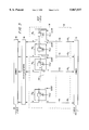
- FIG. 1 is a schematic diagram of a conventional art I,Q modulator circuit
- FIG. 2 is a schematic diagram of an inventive I,Q modulator circuit as disclosed herein and in parent application Ser. No. 08/305,702, now U.S. Pat. No. 5,530,772;
- FIG. 3 is a schematic diagram of an I,Q filtering circuit in accordance with the present invention.
- FIG. 4 is a schematic diagram of an I,Q filtering circuit in accordance with the present invention as applied to CDMA transmission.
- FIG. 3 shows an inventive alternative to the combination of the inverters 42 and the balanced filters 44 of FIG. 2 for realizing a balanced filter.
- An I bitstream or a Q bitstream from delta-sigma convertors 41 is applied to a filter 30 constructed broadly according to FIG. 3, i.e., there is one filter 30 for each of the I and Q bitstreams.
- a filter 30 constructed broadly according to FIG. 3, i.e., there is one filter 30 for each of the I and Q bitstreams.
- one of the balanced transversal filters of FIG. 3 is used for the I-signals, and another one for the Q-signals.
- the I or Q bitstream enters a shift register 50 which is in the form of a chain of shift register stages (50 1 , 50 2 , . . . 50 N ) each comprising a flip-flop (51 1 , 51 2 , . . . 51 N ) having q and q complementary outputs.
- a resistor network 60 consisting of a group of resistors (60 1 , 60 2 . . . 60 N ) of different values R 1 , R 2 , . . . R N are connected to the flip-flop outputs using the q output to obtain a positive weighting value or the q output, as shown at shift register stage 50 3 , if a negative weighting value is desired. How the weights are determined is explained below.
- the other ends of the resistors are connected to a summer 70 which may be simply a summing junction 71.
- An identical set of resistors 80 connects to the flip flop q-outputs where the first network connects to the q outputs and vice-versa, such that the waveform produced at the summer 90 or summing junction 91 of the second resistor network 80 is complementary to the first waveform at the summer 70 or summing junction 71 of the first resistor network 60.
- a 13 MHz reference clock is used as the reference for all bitrates and frequencies.
- the transmitted bitrate is 13 MHz/48.
- 13 MHz as the delta-sigma bitrate output from delta-sigma convertors 41 means that 48 delta-sigma bit outputs will occur per transmitted bit period.
- Shift register 50 can thus conveniently be 48 bits long and the resistors 60 1 -60 48 ("N" in this instance being equal to 48) chosen to obtain a desired impulse response with a duration of one bit period. This impulse response corresponds to a frequency response bandwidth of the order of the bitrate or a few times the bitrate.
- the delta-sigma convertor 31 can comprise a Read Only Memory (ROM) containing 8 precomputed 48-bit patterns of I and Q waveforms corresponding to all possible patterns of three consecutive information bits.
- ROM Read Only Memory
- I,Q waveforms can be created for digital transmitters by means of such a ROM modulator, which relies on being able to truncate the impulse response of the premodulation filter to a reasonable number of bit periods M, where 2 M gives a ROM of a reasonable size.
- the filter can produce, over each bit interval, one of a finite number, 2 M , of possible waveforms.
- the modulation and filtering is achieved simply by feeding the data stream through an M-bit shift register (not shown) which addresses the ROM to output waveforms for that bit interval.
- Each waveform then has an impulse response length which can be up to three information bit periods long, as compared to the one bit period of the filter of FIG. 3 with 48 stages.
- the sharpness of cut-off of a filter response in the frequency domain increases in proportion to the lengths of its impulse response in the time domain. Thus, a long impulse response is desirable to obtain a sharp filtering effect in the frequency domain. Desirable impulse responses are generally several information symbols in length, e.g., 3 symbol periods.
- the sharpness of cut-off is determined by the number symbols each waveform stored in the ROM modulator depends on, while attenuation of components further away from the cut-off point depends on the filtering applied to these delta-sigma waveforms after they emerge from the ROM modulator.
- the filter of FIG. 3 may also be used for generating a filtered, CDMA coded signal, as shown in FIG. 4.
- the DSP 30 supplies convolutionally-coded and interleaved information bits to convertors 41, which are now CDMA code-spreaders 95 instead of the delta-sigma convertors. For example, if the CDMA spreading spreads each coded bit from DSP 30 by a factor of 64, the output chip rate from spreaders 95 will be 64 times the coded information rate, giving in the case of CDMA standard IS-95 a chiprate of 1.2288 Megabits/sec. This chip stream can be used as an input for the filter of FIG. 3.
- the chip stream may be further sampled at four samples per chip to obtain a rate of 4.9152 Megabits/sec which is clocked into a shift register 50 of, for example, 48 stages.
- the total impulse response length of 48 1/4-chips or 12 chips is adequate to allow, by proper choice of weighting resistors 60 1 -60 N , good spectral containment of transmissions.
- FIG. 4 illustrates the application of the present invention to a CDMA system in which the DSP 30 codes analog speech into digital form or accepts digital data signals already in digital form and applies error correction coding.
- the coded speech and data are then converted to I,Q signals representing the vector components of a modulated signal which are further spread-spectrum coded by the code spreading unit 95 to obtain high bitrate I and Q chipstreams.
- the I,Q chipstreams are clocked through shift register stages 50a, 50b at a multiple of (for example, four times) the chiprate and the inverted q or non-inverted q outputs of the shift registers are applied to resistor networks 60a, 60b with the inverse being applied to other resistor networks 80a, 80b.
- the first resistor networks 60a, 80a generate antiphase I-signals forming a balanced signal input to a first balanced RC filter 32a and second resistor networks 60b, 80b form balanced Q-signal outputs to a second balanced RC filter 32b.
- Filters 32a, 32b have only to remove unwanted spectral components above the sampling frequency (of four times the chiprate) and can be integrated RC filters, the main filter frequency response in the vicinity of the chiprate having been accurately determined by the resistor ratios within weighting networks 60a, 60b, 80a, 80b.
- the filtered, balanced I,Q drive signals from filters 32a, 32b are then applied to the balanced inputs of quadrature modulator 43.
- the inventive balanced quadrature modulator may be used advantageously to generate CDMA signals for transmission that have been accurately filtered by balanced transversal filters using resistive weights.
- the weighting values of a transversal filter should follow the coefficients of an inverse Fourier Transform of the desired frequency response.
- the resistor values 60 1 , 60 2 . . . 60 N should be inversely proportional to the Fourier transform of the desired frequency response. This is also equivalent to choosing the weighting resistor values to be inversely proportional to samples on the desired filter impulse response.
- FIGS. 3 and 4 The invention of FIGS. 3 and 4 is amenable to integration in the form of a semiconductor (e.g., silicon) chip.
- Semiconductor chip processes have various means for forming resistors.
- the absolute values of such resistors are hard to control accurately, but an advantage of the invention is that only the ratios of the resistors are of prime importance, and the absolute values are of secondary importance, affecting only the power consumption of the circuit rather than the filter frequency response.
- the resistors should be of high value; high value resistors may be fabricated in a CMOS process for example as long, N-type FETs that are biassed to the ON condition by connecting their gates to the positive supply. The resistor values are proportional then to the total gate length.
Abstract
Description
Claims (8)
Priority Applications (1)
| Application Number | Priority Date | Filing Date | Title |
|---|---|---|---|
| US08/937,248 US5867537A (en) | 1992-10-27 | 1997-09-03 | Balanced tranversal I,Q filters for quadrature modulators |
Applications Claiming Priority (4)
| Application Number | Priority Date | Filing Date | Title |
|---|---|---|---|
| US07/967,027 US5745523A (en) | 1992-10-27 | 1992-10-27 | Multi-mode signal processing |
| US08/305,702 US5530722A (en) | 1992-10-27 | 1994-09-14 | Quadrature modulator with integrated distributed RC filters |
| US62084396A | 1996-03-20 | 1996-03-20 | |
| US08/937,248 US5867537A (en) | 1992-10-27 | 1997-09-03 | Balanced tranversal I,Q filters for quadrature modulators |
Related Parent Applications (1)
| Application Number | Title | Priority Date | Filing Date |
|---|---|---|---|
| US62084396A Continuation | 1992-10-27 | 1996-03-20 |
Publications (1)
| Publication Number | Publication Date |
|---|---|
| US5867537A true US5867537A (en) | 1999-02-02 |
Family
ID=27405112
Family Applications (1)
| Application Number | Title | Priority Date | Filing Date |
|---|---|---|---|
| US08/937,248 Expired - Lifetime US5867537A (en) | 1992-10-27 | 1997-09-03 | Balanced tranversal I,Q filters for quadrature modulators |
Country Status (1)
| Country | Link |
|---|---|
| US (1) | US5867537A (en) |
Cited By (16)
| Publication number | Priority date | Publication date | Assignee | Title |
|---|---|---|---|---|
| US6100827A (en) * | 1998-09-11 | 2000-08-08 | Ericsson Inc. | Modulation systems and methods that compensate for DC offset introduced by the digital-to-analog converter and/or the low pass filter thereof |
| US6137826A (en) * | 1997-11-17 | 2000-10-24 | Ericsson Inc. | Dual-mode modulation systems and methods including oversampling of narrow bandwidth signals |
| WO2001060006A1 (en) * | 2000-02-08 | 2001-08-16 | Ericsson Inc. | COMBINED TRANSMIT FILTER AND D-to-A CONVERTER |
| WO2001060004A1 (en) * | 2000-02-08 | 2001-08-16 | Ericsson, Inc. | 8-psk transmission filtering using reduced look-up tables |
| US20020131526A1 (en) * | 2001-03-16 | 2002-09-19 | Myers Michael H. | Modulation synthesis apparatus for photonic wavelength shifting |
| US20020141487A1 (en) * | 2001-02-22 | 2002-10-03 | Bradley Wayne H. | Signal detection using a CDMA receiver |
| US20030012289A1 (en) * | 2001-04-10 | 2003-01-16 | Bengt Lindoff | Controlled modulation distortion |
| US6577614B1 (en) | 1999-05-27 | 2003-06-10 | Qwest Communications International Inc. | System and method for OTA over CDMA data channel |
| US6647069B1 (en) * | 1998-05-01 | 2003-11-11 | Texas Instruments Incorporated | Method and apparatus for capacity increase and enhanced communications performance in CATV networks |
| GB2398977A (en) * | 2003-02-25 | 2004-09-01 | Roke Manor Research | Baseband signal processor for a spread spectrum receiver |
| EP1798922A1 (en) * | 2005-12-13 | 2007-06-20 | Koninklijke Philips Electronics N.V. | Transmitter device and method of transmission with attenuation of unwanted spectra |
| US20080278277A1 (en) * | 2007-05-08 | 2008-11-13 | Telefonaktiebolaget Lm Ericsson (Publ) | Digitally controllable on-chip resistors and methods |
| US20100142641A1 (en) * | 2007-01-16 | 2010-06-10 | Andreia Cathelin | Method for processing a digital signal in a digital delta-sigma modulator, and digital delta-sigma modulator therefor |
| EP2278703A2 (en) | 2003-08-11 | 2011-01-26 | TELEFONAKTIEBOLAGET LM ERICSSON (publ) | Pseudo-polar modulator for radio transmitters |
| US20110134809A1 (en) * | 2008-08-20 | 2011-06-09 | Qualcomm Incorporated | MUROS Modulation using Linear Baseband Combinations with Linear Gaussian Pulse Shaping for Two users on One Timeslot used by Non-DARP and DARP Remote Stations |
| US20110149778A1 (en) * | 2008-08-20 | 2011-06-23 | Qualcomm Incorporated | Power control method for a geran system to increase geran network capacity |
Citations (42)
| Publication number | Priority date | Publication date | Assignee | Title |
|---|---|---|---|---|
| US2967992A (en) * | 1954-06-15 | 1961-01-10 | Philips Corp | Signal expansion device |
| US3602818A (en) * | 1968-05-17 | 1971-08-31 | Philips Corp | Delay line amplitude compression transmission system |
| US3906166A (en) * | 1973-10-17 | 1975-09-16 | Motorola Inc | Radio telephone system |
| US3949299A (en) * | 1974-11-05 | 1976-04-06 | North Electric Company | Signal coding for telephone communication system |
| US4355401A (en) * | 1979-09-28 | 1982-10-19 | Nippon Electric Co., Ltd. | Radio transmitter/receiver for digital and analog communications system |
| US4400585A (en) * | 1979-11-30 | 1983-08-23 | Motorola, Inc. | Method and apparatus for automatically attempting to seize a radio channel in a multichannel communication system |
| US4455676A (en) * | 1981-03-04 | 1984-06-19 | Nippon Electric Co., Ltd. | Speech processing system including an amplitude level control circuit for digital processing |
| US4493091A (en) * | 1982-05-05 | 1985-01-08 | Dolby Laboratories Licensing Corporation | Analog and digital signal apparatus |
| JPS6046139A (en) * | 1983-08-24 | 1985-03-12 | Nippon Telegr & Teleph Corp <Ntt> | Compander circuit |
| US4713808A (en) * | 1985-11-27 | 1987-12-15 | A T & E Corporation | Watch pager system and communication protocol |
| US4750198A (en) * | 1986-12-12 | 1988-06-07 | Astronet Corporation/Plessey U.K. | Cellular radiotelephone system providing diverse separately-accessible groups of channels |
| US4825448A (en) * | 1986-08-07 | 1989-04-25 | International Mobile Machines Corporation | Subscriber unit for wireless digital telephone system |
| US4835792A (en) * | 1988-01-25 | 1989-05-30 | California Institute Of Technology | Universal FM receiver for mobile communications |
| US4850033A (en) * | 1986-04-04 | 1989-07-18 | U.S. Philips Corp. | Method of and control arrangement for selecting a control channel by a mobile radio station |
| US4857915A (en) * | 1987-10-20 | 1989-08-15 | Telefind Corp. | Paging receiver with paging receiver identification code digits transmitted in order of increasing significance |
| US4903319A (en) * | 1986-07-26 | 1990-02-20 | Nec Corporation | Portable radio telephone having power saver |
| US4903320A (en) * | 1987-03-20 | 1990-02-20 | Fujitsu Limited | Apparatus for selecting control channel in mobile communication system |
| US4989230A (en) * | 1988-09-23 | 1991-01-29 | Motorola, Inc. | Cellular cordless telephone |
| US4996696A (en) * | 1988-03-01 | 1991-02-26 | Shaye Communications Limited | Waveform encoder |
| US5008925A (en) * | 1989-12-20 | 1991-04-16 | Motorola, Inc. | Cellular telephone responsive to service availability for operating on different cellular telephone systems |
| EP0425458A1 (en) * | 1989-10-24 | 1991-05-02 | Telefonaktiebolaget L M Ericsson | A method of adapting a viterbi algorithm to a channel having varying transmission properties, and apparatus for carrying out the method |
| EP0426560A1 (en) * | 1989-11-02 | 1991-05-08 | Matra Communication | Method and apparatus for digital modulation using in-phase and quadrature components |
| US5020076A (en) * | 1990-05-21 | 1991-05-28 | Motorola, Inc. | Hybrid modulation apparatus |
| US5020093A (en) * | 1989-06-23 | 1991-05-28 | Motorola, Inc. | Cellular telephone operable on different cellular telephone systems |
| US5029233A (en) * | 1987-10-09 | 1991-07-02 | Motorola, Inc. | Radio arrangement having two radios sharing circuitry |
| US5048059A (en) * | 1988-09-19 | 1991-09-10 | Telefonaktiebolaget Lm Ericsson | Log-polar signal processing |
| US5068818A (en) * | 1989-06-06 | 1991-11-26 | Mitbushi Denki Kabushiki Kaisha | Hardware implemented moving average processor |
| US5079550A (en) * | 1989-10-27 | 1992-01-07 | Crystal Semiconductor Corporation | Combining continuous time and discrete time signal processing in a delta-sigma modulator |
| US5084669A (en) * | 1990-03-08 | 1992-01-28 | Telefonaktiebolaget L M Ericsson | Direct phase digitization |
| US5119397A (en) * | 1990-04-26 | 1992-06-02 | Telefonaktiebolaget L M Ericsson | Combined analog and digital cellular telephone system having a secondary set of control channels |
| US5124703A (en) * | 1990-04-05 | 1992-06-23 | Matsushita Electric Industrial Co., Ltd. | Digital signal requantizing circuit using multistage noise shaping |
| US5136612A (en) * | 1990-12-31 | 1992-08-04 | At&T Bell Laboratories | Method and apparatus for reducing effects of multiple access interference in a radio receiver in a code division multiple access communication system |
| US5150362A (en) * | 1989-09-13 | 1992-09-22 | Telefonaktiebolaget L M Ericsson | Beacon carrier |
| US5163159A (en) * | 1990-07-30 | 1992-11-10 | Motorola, Inc. | Dual mode automatic frequency control |
| US5189593A (en) * | 1991-11-04 | 1993-02-23 | Motorola, Inc. | Integrated distributed resistive-capacitive network |
| US5220275A (en) * | 1991-07-26 | 1993-06-15 | Ericsson Ge Mobile Communication Holding, Inc. | Accumulator phase digitizer |
| WO1993014588A1 (en) * | 1992-01-16 | 1993-07-22 | Qualcomm Incorporated | Method and apparatus for the formatting of data for transmission |
| US5243346A (en) * | 1990-12-19 | 1993-09-07 | Nec Corporation | Digital-to-analog converting device using decoders and parallel-to-serial converters |
| US5251232A (en) * | 1991-03-06 | 1993-10-05 | Mitsubishi Denki Kabushiki Kaisha | Radio communication apparatus |
| US5293406A (en) * | 1991-03-11 | 1994-03-08 | Nippon Telegraph And Telephone Corporation | Quadrature amplitude modulator with distortion compensation |
| WO1996008865A2 (en) * | 1994-09-14 | 1996-03-21 | Ericsson Inc. | Quadrature modulator with integrated distributed rc filters |
| US5548541A (en) * | 1994-08-08 | 1996-08-20 | Interstate Electronics Corporation | Finite impulse response filter for modulator in digital data transmission system |
-
1997
- 1997-09-03 US US08/937,248 patent/US5867537A/en not_active Expired - Lifetime
Patent Citations (43)
| Publication number | Priority date | Publication date | Assignee | Title |
|---|---|---|---|---|
| US2967992A (en) * | 1954-06-15 | 1961-01-10 | Philips Corp | Signal expansion device |
| US3602818A (en) * | 1968-05-17 | 1971-08-31 | Philips Corp | Delay line amplitude compression transmission system |
| US3906166A (en) * | 1973-10-17 | 1975-09-16 | Motorola Inc | Radio telephone system |
| US3949299A (en) * | 1974-11-05 | 1976-04-06 | North Electric Company | Signal coding for telephone communication system |
| US4355401A (en) * | 1979-09-28 | 1982-10-19 | Nippon Electric Co., Ltd. | Radio transmitter/receiver for digital and analog communications system |
| US4400585A (en) * | 1979-11-30 | 1983-08-23 | Motorola, Inc. | Method and apparatus for automatically attempting to seize a radio channel in a multichannel communication system |
| US4455676A (en) * | 1981-03-04 | 1984-06-19 | Nippon Electric Co., Ltd. | Speech processing system including an amplitude level control circuit for digital processing |
| US4493091A (en) * | 1982-05-05 | 1985-01-08 | Dolby Laboratories Licensing Corporation | Analog and digital signal apparatus |
| JPS6046139A (en) * | 1983-08-24 | 1985-03-12 | Nippon Telegr & Teleph Corp <Ntt> | Compander circuit |
| US4713808A (en) * | 1985-11-27 | 1987-12-15 | A T & E Corporation | Watch pager system and communication protocol |
| US4850033A (en) * | 1986-04-04 | 1989-07-18 | U.S. Philips Corp. | Method of and control arrangement for selecting a control channel by a mobile radio station |
| US4903319A (en) * | 1986-07-26 | 1990-02-20 | Nec Corporation | Portable radio telephone having power saver |
| US4825448A (en) * | 1986-08-07 | 1989-04-25 | International Mobile Machines Corporation | Subscriber unit for wireless digital telephone system |
| US4750198A (en) * | 1986-12-12 | 1988-06-07 | Astronet Corporation/Plessey U.K. | Cellular radiotelephone system providing diverse separately-accessible groups of channels |
| US4903320A (en) * | 1987-03-20 | 1990-02-20 | Fujitsu Limited | Apparatus for selecting control channel in mobile communication system |
| US5029233A (en) * | 1987-10-09 | 1991-07-02 | Motorola, Inc. | Radio arrangement having two radios sharing circuitry |
| US4857915A (en) * | 1987-10-20 | 1989-08-15 | Telefind Corp. | Paging receiver with paging receiver identification code digits transmitted in order of increasing significance |
| US4835792A (en) * | 1988-01-25 | 1989-05-30 | California Institute Of Technology | Universal FM receiver for mobile communications |
| US4996696A (en) * | 1988-03-01 | 1991-02-26 | Shaye Communications Limited | Waveform encoder |
| US5048059A (en) * | 1988-09-19 | 1991-09-10 | Telefonaktiebolaget Lm Ericsson | Log-polar signal processing |
| US4989230A (en) * | 1988-09-23 | 1991-01-29 | Motorola, Inc. | Cellular cordless telephone |
| US5068818A (en) * | 1989-06-06 | 1991-11-26 | Mitbushi Denki Kabushiki Kaisha | Hardware implemented moving average processor |
| US5020093A (en) * | 1989-06-23 | 1991-05-28 | Motorola, Inc. | Cellular telephone operable on different cellular telephone systems |
| US5150362A (en) * | 1989-09-13 | 1992-09-22 | Telefonaktiebolaget L M Ericsson | Beacon carrier |
| EP0425458A1 (en) * | 1989-10-24 | 1991-05-02 | Telefonaktiebolaget L M Ericsson | A method of adapting a viterbi algorithm to a channel having varying transmission properties, and apparatus for carrying out the method |
| US5079550A (en) * | 1989-10-27 | 1992-01-07 | Crystal Semiconductor Corporation | Combining continuous time and discrete time signal processing in a delta-sigma modulator |
| EP0426560A1 (en) * | 1989-11-02 | 1991-05-08 | Matra Communication | Method and apparatus for digital modulation using in-phase and quadrature components |
| US5008925A (en) * | 1989-12-20 | 1991-04-16 | Motorola, Inc. | Cellular telephone responsive to service availability for operating on different cellular telephone systems |
| US5084669A (en) * | 1990-03-08 | 1992-01-28 | Telefonaktiebolaget L M Ericsson | Direct phase digitization |
| US5124703A (en) * | 1990-04-05 | 1992-06-23 | Matsushita Electric Industrial Co., Ltd. | Digital signal requantizing circuit using multistage noise shaping |
| US5119397A (en) * | 1990-04-26 | 1992-06-02 | Telefonaktiebolaget L M Ericsson | Combined analog and digital cellular telephone system having a secondary set of control channels |
| US5020076A (en) * | 1990-05-21 | 1991-05-28 | Motorola, Inc. | Hybrid modulation apparatus |
| US5163159A (en) * | 1990-07-30 | 1992-11-10 | Motorola, Inc. | Dual mode automatic frequency control |
| US5243346A (en) * | 1990-12-19 | 1993-09-07 | Nec Corporation | Digital-to-analog converting device using decoders and parallel-to-serial converters |
| US5136612A (en) * | 1990-12-31 | 1992-08-04 | At&T Bell Laboratories | Method and apparatus for reducing effects of multiple access interference in a radio receiver in a code division multiple access communication system |
| US5251232A (en) * | 1991-03-06 | 1993-10-05 | Mitsubishi Denki Kabushiki Kaisha | Radio communication apparatus |
| US5293406A (en) * | 1991-03-11 | 1994-03-08 | Nippon Telegraph And Telephone Corporation | Quadrature amplitude modulator with distortion compensation |
| US5220275A (en) * | 1991-07-26 | 1993-06-15 | Ericsson Ge Mobile Communication Holding, Inc. | Accumulator phase digitizer |
| US5189593A (en) * | 1991-11-04 | 1993-02-23 | Motorola, Inc. | Integrated distributed resistive-capacitive network |
| WO1993014588A1 (en) * | 1992-01-16 | 1993-07-22 | Qualcomm Incorporated | Method and apparatus for the formatting of data for transmission |
| US5530722A (en) * | 1992-10-27 | 1996-06-25 | Ericsson Ge Mobile Communications Inc. | Quadrature modulator with integrated distributed RC filters |
| US5548541A (en) * | 1994-08-08 | 1996-08-20 | Interstate Electronics Corporation | Finite impulse response filter for modulator in digital data transmission system |
| WO1996008865A2 (en) * | 1994-09-14 | 1996-03-21 | Ericsson Inc. | Quadrature modulator with integrated distributed rc filters |
Non-Patent Citations (24)
| Title |
|---|
| "Audio compander squelches hiss and hum better than Dolby system", electronics, vol. 52, No. 4, Feb. 15, 1979, pp. 70, 72. |
| A. Yasuda et al., "A Small-Size Adder-Free π/4-Shift QPSK Signal Generator," IEEE 1995 Custom Integrated Circuits Conference, May 1, 1995, pp. 315-318. |
| A. Yasuda et al., A Small Size Adder Free /4 Shift QPSK Signal Generator, IEEE 1995 Custom Integrated Circuits Conference, May 1, 1995, pp. 315 318. * |
| Audio compander squelches hiss and hum better than Dolby system , electronics, vol. 52, No. 4, Feb. 15, 1979, pp. 70, 72. * |
| Ericsson Review, "Introduction of Digital Cellular Systems in North America", F. Lindell and K. Raith, No. 2, 1990, vol. 67. |
| Ericsson Review, Introduction of Digital Cellular Systems in North America , F. Lindell and K. Raith, No. 2, 1990, vol. 67. * |
| F. Harris, "Implementing Waveform Shaping Filters to Pre-Equalize Gain and Phase Distortion of the Analog Signal Processing Path in DSP Based Modems," Proceedings of the Military Communications Conference, Oct. 2-5, 1994, New York, US, pp. 633-638. |
| F. Harris, Implementing Waveform Shaping Filters to Pre Equalize Gain and Phase Distortion of the Analog Signal Processing Path in DSP Based Modems, Proceedings of the Military Communications Conference, Oct. 2 5, 1994, New York, US, pp. 633 638. * |
| Global News, "Hughes Network Systems Jumps into the Cellular Arena with GM Backing", Feb. 1991, pp. 15-16. |
| Global News, Hughes Network Systems Jumps into the Cellular Arena with GM Backing , Feb. 1991, pp. 15 16. * |
| Hongying Yan et al., "DSP Implementation of GFSK, GMSK and FQPSK Modulated Wireless Systems," RF Design, vol. 18, No. 6, Jun. 1, 1995, US, pp. 26-34. |
| Hongying Yan et al., DSP Implementation of GFSK, GMSK and FQPSK Modulated Wireless Systems, RF Design, vol. 18, No. 6, Jun. 1, 1995, US, pp. 26 34. * |
| IEEE Communications Magazine, "Trends in Cellular and Cordless Communications", D.J. Goodman, Jun. 1991, pp. 31-40. |
| IEEE Communications Magazine, Trends in Cellular and Cordless Communications , D.J. Goodman, Jun. 1991, pp. 31 40. * |
| J.K. Hinderling et al., "CDMA Mobile Station Modem ASIC," IEEE Journal of Solid-State Circuits, vol. 28, No. 3, Mar. 1993, New York, US, pp. 253-260. |
| J.K. Hinderling et al., CDMA Mobile Station Modem ASIC, IEEE Journal of Solid State Circuits, vol. 28, No. 3, Mar. 1993, New York, US, pp. 253 260. * |
| Motorola, "DYNA T-A-C 6000X Universal Mobile Telephone", 1984. |
| Motorola, DYNA T A C 6000X Universal Mobile Telephone , 1984. * |
| Nobuaki Imai, et al., "An Extremely Accurate Quadrature Modulator IC Using Phase Detection Method and Its Application to Multilevel QAM Systems," IEICE Transactions on Electronics, vol. E75-C, No. 6 (Jun. 1992), pp. 674-682. |
| Nobuaki Imai, et al., An Extremely Accurate Quadrature Modulator IC Using Phase Detection Method and Its Application to Multilevel QAM Systems, IEICE Transactions on Electronics, vol. E75 C, No. 6 (Jun. 1992), pp. 674 682. * |
| R. Fisher, "Dual Mode Mobile Unit For Next Generation Digital Narrow Channel Cellular Telephone System," 38th IEEE Vehicular Tech. Conf., 1988, pp. 543-547. |
| R. Fisher, Dual Mode Mobile Unit For Next Generation Digital Narrow Channel Cellular Telephone System, 38th IEEE Vehicular Tech. Conf., 1988, pp. 543 547. * |
| Tarallo et al., "Modulation Techniques for Digital Cellular Systems," 38th IEEE Veh. Tech. Conf., 1988, pp. 245-248. |
| Tarallo et al., Modulation Techniques for Digital Cellular Systems, 38th IEEE Veh. Tech. Conf., 1988, pp. 245 248. * |
Cited By (34)
| Publication number | Priority date | Publication date | Assignee | Title |
|---|---|---|---|---|
| US6535561B2 (en) | 1997-11-17 | 2003-03-18 | Ericsson Inc. | Dual-mode modulation systems and methods including oversampling of narrow bandwidth signals and DC offset compensation |
| US6137826A (en) * | 1997-11-17 | 2000-10-24 | Ericsson Inc. | Dual-mode modulation systems and methods including oversampling of narrow bandwidth signals |
| US7136422B2 (en) | 1998-05-01 | 2006-11-14 | Texas Instruments Incorporated | Method and apparatus for capacity increase and enhanced communications performance in CATV networks |
| US20060008039A1 (en) * | 1998-05-01 | 2006-01-12 | Mordechai Segal | Method and apparatus for capacity increase and enhanced communications performance in CATV networks |
| US6647069B1 (en) * | 1998-05-01 | 2003-11-11 | Texas Instruments Incorporated | Method and apparatus for capacity increase and enhanced communications performance in CATV networks |
| US6100827A (en) * | 1998-09-11 | 2000-08-08 | Ericsson Inc. | Modulation systems and methods that compensate for DC offset introduced by the digital-to-analog converter and/or the low pass filter thereof |
| US6577614B1 (en) | 1999-05-27 | 2003-06-10 | Qwest Communications International Inc. | System and method for OTA over CDMA data channel |
| US7046738B1 (en) * | 2000-02-08 | 2006-05-16 | Ericsson Inc. | 8-PSK transmit filtering using reduced look up tables |
| US6429798B1 (en) | 2000-02-08 | 2002-08-06 | Ericsson Inc. | Combined transmit filter and D-to-A converter |
| WO2001060004A1 (en) * | 2000-02-08 | 2001-08-16 | Ericsson, Inc. | 8-psk transmission filtering using reduced look-up tables |
| WO2001060006A1 (en) * | 2000-02-08 | 2001-08-16 | Ericsson Inc. | COMBINED TRANSMIT FILTER AND D-to-A CONVERTER |
| US20020141487A1 (en) * | 2001-02-22 | 2002-10-03 | Bradley Wayne H. | Signal detection using a CDMA receiver |
| US6996158B2 (en) | 2001-02-22 | 2006-02-07 | Freescale Semiconductors, Inc. | Signal detection using a CDMA receiver |
| US20020131526A1 (en) * | 2001-03-16 | 2002-09-19 | Myers Michael H. | Modulation synthesis apparatus for photonic wavelength shifting |
| US20030012289A1 (en) * | 2001-04-10 | 2003-01-16 | Bengt Lindoff | Controlled modulation distortion |
| US7020070B2 (en) * | 2001-04-10 | 2006-03-28 | Telefonaktiebolaget L M Ericsson (Publ) | Selectively controlled modulation distortion of an IQ-baseband signal |
| GB2398977A (en) * | 2003-02-25 | 2004-09-01 | Roke Manor Research | Baseband signal processor for a spread spectrum receiver |
| GB2398977B (en) * | 2003-02-25 | 2005-11-30 | Roke Manor Research | Baseband signal processor |
| EP2278703A2 (en) | 2003-08-11 | 2011-01-26 | TELEFONAKTIEBOLAGET LM ERICSSON (publ) | Pseudo-polar modulator for radio transmitters |
| WO2007069192A3 (en) * | 2005-12-13 | 2007-09-20 | Nxp Bv | Transmitter device and method of transmission with attenuation of unwanted spectra |
| US8279970B2 (en) | 2005-12-13 | 2012-10-02 | St-Ericsson Sa | Transmission spectra |
| US20090168921A1 (en) * | 2005-12-13 | 2009-07-02 | Nxp B.V. | Transmission spectra |
| WO2007069192A2 (en) * | 2005-12-13 | 2007-06-21 | Nxp B.V. | Transmitter device and method of transmission with attenuation of unwanted spectra |
| EP1798922A1 (en) * | 2005-12-13 | 2007-06-20 | Koninklijke Philips Electronics N.V. | Transmitter device and method of transmission with attenuation of unwanted spectra |
| US8594226B2 (en) * | 2007-01-16 | 2013-11-26 | Stmicroelectronics Sa | Method for processing a digital signal in a digital delta-sigma modulator, and digital delta-sigma modulator therefor |
| US20100142641A1 (en) * | 2007-01-16 | 2010-06-10 | Andreia Cathelin | Method for processing a digital signal in a digital delta-sigma modulator, and digital delta-sigma modulator therefor |
| US7602327B2 (en) * | 2007-05-08 | 2009-10-13 | Telefonaktiebolaget Lm Ericsson (Publ) | Digitally controllable on-chip resistors and methods |
| US20080278277A1 (en) * | 2007-05-08 | 2008-11-13 | Telefonaktiebolaget Lm Ericsson (Publ) | Digitally controllable on-chip resistors and methods |
| US20110149778A1 (en) * | 2008-08-20 | 2011-06-23 | Qualcomm Incorporated | Power control method for a geran system to increase geran network capacity |
| US20110134809A1 (en) * | 2008-08-20 | 2011-06-09 | Qualcomm Incorporated | MUROS Modulation using Linear Baseband Combinations with Linear Gaussian Pulse Shaping for Two users on One Timeslot used by Non-DARP and DARP Remote Stations |
| US8687525B2 (en) | 2008-08-20 | 2014-04-01 | Qualcomm Incorporated | Co-channel communication methods, systems, and devices |
| US8705411B2 (en) | 2008-08-20 | 2014-04-22 | Qualcomm Incorporated | MUROS modulation using linear baseband combinations with linear gaussian pulse shaping for two users on one timeslot used by non-DARP and DARP remote stations |
| US8867382B2 (en) | 2008-08-20 | 2014-10-21 | Qualcomm Incorporated | Power control method for a GERAN system to increase GERAN network capacity |
| TWI478545B (en) * | 2008-08-20 | 2015-03-21 | Qualcomm Inc | Muros modulation using linear baseband combinations with linear gaussian pulse shaping for two users on one timeslot used by non-darp and darp remote stations |
Similar Documents
| Publication | Publication Date | Title |
|---|---|---|
| US5867537A (en) | Balanced tranversal I,Q filters for quadrature modulators | |
| US6628728B1 (en) | Nyquist filter and method | |
| EP0194903B1 (en) | Digital quadrature amplitude modulator | |
| JP4395229B2 (en) | Digital / analog conversion electronics | |
| US6683905B1 (en) | Dual-mode receiver | |
| US5027372A (en) | Differential phase shift keying modulator | |
| US6489908B2 (en) | Wireless local loop terminal and system having high speed, high resolution, digital-to-analog converter with off-line sigma-delta conversion and storage | |
| WO1999038298A1 (en) | Pulse shaping according to modulation scheme | |
| DE60210592T2 (en) | Wireless subscriber terminal and system with high-speed and high-resolution analog-to-digital converter with off-line sigma-delta conversion and storage | |
| US4825452A (en) | Digital FSK demodulator | |
| EP0888681B1 (en) | Balanced transversal i,q filters for quadrature modulators | |
| JP2004509522A (en) | How to generate mobile communication signals of different mobile radio standards | |
| CA2037090C (en) | Modem comprising saw filters having opposite passband delay characteristics | |
| JPH07327056A (en) | Frequency modulator | |
| AU748932B2 (en) | Method and arrangement for signal modulation | |
| Song et al. | Design of improved GMSK quadrature modulator | |
| Babu et al. | GSM-EDGE modulators for 2.5 G system, an efficient parallel implementation on FPGA | |
| GB2337670A (en) | Defining a pulse function shape for acting on a data stream for transmission |
Legal Events
| Date | Code | Title | Description |
|---|---|---|---|
| STCF | Information on status: patent grant |
Free format text: PATENTED CASE |
|
| FPAY | Fee payment |
Year of fee payment: 4 |
|
| REMI | Maintenance fee reminder mailed | ||
| FPAY | Fee payment |
Year of fee payment: 8 |
|
| FPAY | Fee payment |
Year of fee payment: 12 |
|
| AS | Assignment |
Owner name: ERICSSON GE MOBILE COMMUNICATIONS INC., NORTH CARO Free format text: ASSIGNMENT OF ASSIGNORS INTEREST;ASSIGNOR:DENT, PAUL W.;REEL/FRAME:030258/0295 Effective date: 19941026 |
|
| AS | Assignment |
Owner name: ERICSSON INC., TEXAS Free format text: CHANGE OF NAME;ASSIGNOR:ERICSSON GE MOBILE COMMUNICATIONS INC.;REEL/FRAME:030293/0047 Effective date: 19941222 |
|
| AS | Assignment |
Owner name: CLUSTER LLC, DELAWARE Free format text: ASSIGNMENT OF ASSIGNORS INTEREST;ASSIGNOR:ERICSSON INC.;REEL/FRAME:030303/0370 Effective date: 20130211 |
|
| AS | Assignment |
Owner name: UNWIRED PLANET, LLC, NEVADA Free format text: ASSIGNMENT OF ASSIGNORS INTEREST;ASSIGNOR:CLUSTER LLC;REEL/FRAME:030319/0023 Effective date: 20130213 |
|
| AS | Assignment |
Owner name: CLUSTER LLC, SWEDEN Free format text: NOTICE OF GRANT OF SECURITY INTEREST IN PATENTS;ASSIGNOR:UNWIRED PLANET, LLC;REEL/FRAME:030369/0601 Effective date: 20130213 |