US5880923A - Method and apparatus for improved retention of a semiconductor wafer within a semiconductor wafer processing system - Google Patents
Method and apparatus for improved retention of a semiconductor wafer within a semiconductor wafer processing system Download PDFInfo
- Publication number
- US5880923A US5880923A US08/871,741 US87174197A US5880923A US 5880923 A US5880923 A US 5880923A US 87174197 A US87174197 A US 87174197A US 5880923 A US5880923 A US 5880923A
- Authority
- US
- United States
- Prior art keywords
- electrode
- electrodes
- chucking
- voltage
- wafer
- Prior art date
- Legal status (The legal status is an assumption and is not a legal conclusion. Google has not performed a legal analysis and makes no representation as to the accuracy of the status listed.)
- Expired - Fee Related
Links
Images


Classifications
-
- H—ELECTRICITY
- H01—ELECTRIC ELEMENTS
- H01L—SEMICONDUCTOR DEVICES NOT COVERED BY CLASS H10
- H01L21/00—Processes or apparatus adapted for the manufacture or treatment of semiconductor or solid state devices or of parts thereof
- H01L21/67—Apparatus specially adapted for handling semiconductor or electric solid state devices during manufacture or treatment thereof; Apparatus specially adapted for handling wafers during manufacture or treatment of semiconductor or electric solid state devices or components ; Apparatus not specifically provided for elsewhere
- H01L21/68—Apparatus specially adapted for handling semiconductor or electric solid state devices during manufacture or treatment thereof; Apparatus specially adapted for handling wafers during manufacture or treatment of semiconductor or electric solid state devices or components ; Apparatus not specifically provided for elsewhere for positioning, orientation or alignment
-
- H—ELECTRICITY
- H01—ELECTRIC ELEMENTS
- H01L—SEMICONDUCTOR DEVICES NOT COVERED BY CLASS H10
- H01L21/00—Processes or apparatus adapted for the manufacture or treatment of semiconductor or solid state devices or of parts thereof
- H01L21/67—Apparatus specially adapted for handling semiconductor or electric solid state devices during manufacture or treatment thereof; Apparatus specially adapted for handling wafers during manufacture or treatment of semiconductor or electric solid state devices or components ; Apparatus not specifically provided for elsewhere
- H01L21/683—Apparatus specially adapted for handling semiconductor or electric solid state devices during manufacture or treatment thereof; Apparatus specially adapted for handling wafers during manufacture or treatment of semiconductor or electric solid state devices or components ; Apparatus not specifically provided for elsewhere for supporting or gripping
- H01L21/6831—Apparatus specially adapted for handling semiconductor or electric solid state devices during manufacture or treatment thereof; Apparatus specially adapted for handling wafers during manufacture or treatment of semiconductor or electric solid state devices or components ; Apparatus not specifically provided for elsewhere for supporting or gripping using electrostatic chucks
- H01L21/6833—Details of electrostatic chucks
-
- Y—GENERAL TAGGING OF NEW TECHNOLOGICAL DEVELOPMENTS; GENERAL TAGGING OF CROSS-SECTIONAL TECHNOLOGIES SPANNING OVER SEVERAL SECTIONS OF THE IPC; TECHNICAL SUBJECTS COVERED BY FORMER USPC CROSS-REFERENCE ART COLLECTIONS [XRACs] AND DIGESTS
- Y10—TECHNICAL SUBJECTS COVERED BY FORMER USPC
- Y10T—TECHNICAL SUBJECTS COVERED BY FORMER US CLASSIFICATION
- Y10T279/00—Chucks or sockets
- Y10T279/23—Chucks or sockets with magnetic or electrostatic means
Definitions
- the invention relates generally to an apparatus and a concomitant method for retaining a workpiece within a semiconductor wafer processing system and, more specifically, to an improved electrostatic chuck that provides zones of varying chucking force to reduce heat transfer gas leakage, and improve heat transfer gas layer uniformity beneath the workpiece.
- Electrostatic chucks are used for retaining a workpiece in various applications ranging from holding a sheet of paper in a computer graphics plotter to holding a semiconductor wafer within a semiconductor wafer process chamber.
- electrostatic chucks vary in design, they all are based on the principle of applying a voltage to one or more electrodes in the chuck so as to induce opposite polarity charges in the workpiece and electrodes, respectively. The electrostatic attractive force between the opposite charges presses the workpiece against the chuck, thereby retaining the workpiece.
- electrostatic chucks are used for clamping wafers to a pedestal during processing. Since the materials and processes used to process a wafer are extremely temperature sensitive, temperature control is an important aspect of wafer processing. Should the materials be exposed to excessive temperature fluctuations resulting from poor heat transfer during processing, performance of the wafer process may be compromised resulting in wafer damage.
- the pedestal may form a chucking electrode as well as a heat sink or heater as used in etching, physical vapor deposition (PVD) or chemical vapor deposition (CVD) applications.
- an inert heat transfer gas is pumped into the volume formed by the interstitial spaces between the support surface of the chuck and the wafer. This gas acts as a thermal heat transfer medium from the wafer to the chuck that has better heat transfer characteristics than the vacuum it replaces.
- the electrostatic chuck or the pedestal which supports the chuck contains an outer diameter raised rim.
- the rim is approximately the same diameter as that of the semiconductor wafer. As such, the wafer is supported at its outer edge by this rim.
- an electrostatic clamping force is applied to the chuck, the wafer is pulled down to the support surface effectively creating a seal on the backside of the wafer at the rim.
- a heat transfer gas into the process chamber is introduced to the backside of the wafer to improve heat conduction away from the wafer.
- the disadvantages heretofore associated with the prior art are overcome by an inventive configuration of an electrostatic chuck used for retaining semiconductor wafers in semiconductor wafer processing equipment.
- the electrostatic chuck contains a wafer support having a surface. Beneath the surface of the wafer support is a number of electrodes arranged and defining a number of chucking zones. The electrodes are energized by a number of DC voltages thereby creating a different chucking force in each of the chucking zones.
- the invention includes a method of retaining a substrate upon a substrate support comprising the steps of biasing at least one of the electrodes with a first voltage of a first magnitude and biasing each previously unbiased electrode with a voltage of unequal magnitude of the initially biased electrode and every other previously unbiased electrode such that a different chucking force exists in every zone.
- nonuniform heat transfer gas layer formation is greatly reduced.
- the amount of force applied to a particular area of the wafer is controlled. For example, a greater force is applied at the wafer edge where heat transfer gas leakage occurs and a lesser force is applied near the center where excessive force can prevent heat transfer gas diffusion into interstitial regions.
- Customizing the chucking force across the backside of the wafer provides increased heat transfer gas uniformity and thus promotes temperature uniformity across the wafer.
- FIG. 1 is a cross-sectional view of a prior art electrostatic chuck assembly with a semiconductor wafer clamped to a support surface;
- FIG. 2 is a schematic representational view of the equivalent circuit created by the prior art electrostatic chuck assembly of FIG. 1;
- FIG. 3 is a schematic representational view of the equivalent circuit created by the present invention.
- FIG. 4 is a top view of a first embodiment of the apparatus of the present invention.
- FIG. 5 is a top view of a second embodiment of the apparatus of the present invention.
- FIG. 6 is a top view of a third embodiment of the apparatus of the present invention.
- FIG. 1 depicts a cross-sectional view of a conventional electrostatic chuck assembly 100 used in supporting and clamping semiconductor wafers in a reaction chamber (not shown) during processing.
- the electrostatic chuck assembly contains a pedestal 102 supporting an electrostatic chuck 104.
- the operation of a conventional electrostatic chuck is disclosed in U.S. Pat. No. 5,350,479 issued Sep. 27, 1994 to Applied Materials, Inc. of Santa Clara, Calif.
- the electrostatic chuck 104 has one or more electrodes 110 sandwiched between two dielectric layers 112a and 112b to transform electrical power into an electrostatic clamping force 114.
- the dielectric is a semi-pliant material, typically polyimide, adhered to a top surface 116 of the pedestal 102.
- the chuck can be a ceramic slab with electrodes embedded beneath the surface.
- a top surface 106 of the electrostatic chuck 104 in turn supports a substrate material 108, typically a semiconductor wafer.
- the chucking force of a given electrostatic chuck is defined by the equation ##EQU1## where A is the area of the electrodes, V is the voltage drop between the electrode and the backside of the wafer, d is the thickness of the dielectric layer and ⁇ is the dielectric constant of the dielectric material.
- the chucking force is strongly affected by the potential difference between the electrode and the backside of the wafer.
- the chucking force is created by a difference in potential between two electrodes of a bipolar chuck. That is, equal and opposite charges across each of the electrodes establish an electric field through the dielectric material and across a portion of the chuck surface. This electric field induces charges to migrate to the backside of the wafer and electrostatically clamp the wafer to the chuck.
- FIG. 2 is a schematic representation of the equivalent circuit of a wafer clamped to a bipolar chuck.
- Each electrode 110 and a portion of the wafer backside 202 form the plates of each capacitor C 1 and C 2 .
- the capacitance between the plates is determined by the dielectric constant ⁇ of the dielectric material between the electrode and wafer.
- the chucking force created by one electrode at, for example, potential V 1 and the backside of the wafer at potential V b is ##EQU2##
- the electrodes are maintained at equal but opposite voltages to induce equal force on each half of the wafer.
- FIG. 3 is an equivalent circuit having voltages V 1 , V 2 . . . V n applied to the additional electrodes. Electrode placement and applied voltage can be strategically determined and altered to increase chucking force in a zone where it is most needed and decrease where excessive force is detrimental to wafer processing.
- FIG. 4 depicts one embodiment of the present invention having a concentric ring electrode arrangement 400 to form a customized bipolar electrostatic chuck.
- a first set of electrodes 406 and 408 are arranged concentrically about the electrostatic chuck near the edge 410 of the chuck forming one chucking zone.
- a second set of electrodes 402 and 404 are arranged concentrically about the electrostatic chuck and radially inward of the first set forming a second chucking zone.
- one electrode from the first set is biased positively with DC voltage V 1 and the other electrode is biased negatively with the same magnitude voltage.
- the second set of electrodes is biased with a different DC voltage V 2 .
- V 1 >V 2 so that a greater chucking force is applied at the edge of the chuck where heat transfer gas has been known to leak into the chamber.
- V 2 provides sufficient force to retain the wafer but not an excessive force that blocks diffusion of the heat transfer gas throughout the interstitial spaces under the wafer.
- the different DC voltages may come from different power supplies or from the same power supply that is capable of delivering different voltages (i.e., a transformer tapped at various locations on the output coil).
- a monopolar chuck includes a plurality monopolar electrodes forming a plurality of chucking zones at various voltage levels to further customize the chucking force profile.
- FIG. 5 depicts such a monopolar chuck 500 as a second embodiment of the invention.
- each of the concentric ring electrodes 502, 504, 506 and 508 is biased at respectively different voltage levels V 1 , V 2 , V 3 and V 4 .
- V 1 >V 2 >V 3 >V 4 so that the greatest chucking force exists at the chuck edge.
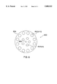
- FIG. 6 depicts another embodiment wherein a number (e.g., nineteen) of pads (602, 604 and 606) form the chucking zones. Each pad is biased with a different voltage thereby pulling the wafer down with greatest force at the pad with the highest applied voltage. If heat transfer gas leakage is detected at a certain location along the chuck edge, the biasing on the electrodes nearest the leak can be altered to clamp the wafer with greater force in this location without losing seal integrity at other points along the edge.
- a number e.g., nineteen
- the area A of the electrode is also a factor in determining chucking force.
- the electrode pattern can be designed with varying size electrodes with different or the same voltage applied to create the unequal chucking force profile.
- the pads have different size diameters. Specifically, larger diameter pads 602 are located at the outer edge 608 of the chuck 600 to provide a strong chucking force. Smaller diameter pads 604 are located inwards of the larger pads where a reduced chucking force is adequate. The smallest pad 606 is located in the center where the chucking force is still capable of clamping the wafer to the support surface, but does not restrict diffusion of heat transfer gas to interstitial spaces proximate the center of the support surface.
- multiple chucking zones can prove useful in other types of applications.
- multiple chucking zones can enhance the chucking capability of non-flat surfaces.
- spherical- or dome-shaped pedestals need a greater chucking force at their edge where a wafer tends to bow away from the chuck surface.
- the novel apparatus can be designed in any of the configurations described above or in any other manner by those skilled in the art to facilitate wafer edge clamping to facilitate use of a shaped pedestal.
- the creation of wafer chucking zones of unequal force in an electrostatic chuck provides a solution to the problem of nonuniform heat transfer gas layer formation beneath the backside of a semiconductor wafer during wafer processing.
- Nonuniformity of the heat transfer gas layer caused by a variety of physical and environmental reasons, is eliminated by controlling the amount of force applied to a particular area of the wafer. For example, a greater force is applied at the wafer edge where heat transfer gas leakage is the source for non-uniformity of the heat transfer gas layer. A lesser force is applied near the center where excessive force can prevent heat transfer gas diffusion into interstitial regions.
- Customizing the chucking force across the backside of the wafer provides increased heat transfer gas uniformity and thus uniformity of the temperature across the wafer. Achieving greater temperature uniformity of the wafer results in a better quality and higher yield end product.
Abstract
Method and apparatus for retaining a semiconductor wafer upon a pedestal within semiconductor wafer processing equipment. An electrostatic chuck contains a wafer support having a surface. Embedded beneath the surface is a number of electrodes defining a number of chucking zones. The electrodes are energized by a number of non-zero voltages thereby creating a variable, non-zero chucking force in each of the chucking zones. The method of retaining a substrate to a substrate support consists of biasing at least one of the electrodes with a first voltage of a first magnitude and biasing each previously unbiased electrode with a voltage of unequal magnitude of the initially biased electrode and every other previously unbiased electrode such that a non-zero chucking force exists in every zone. Wafer chucking zones of differing force improve uniformity of heat transfer gas layer distribution.
Description
1. Field of the Invention
The invention relates generally to an apparatus and a concomitant method for retaining a workpiece within a semiconductor wafer processing system and, more specifically, to an improved electrostatic chuck that provides zones of varying chucking force to reduce heat transfer gas leakage, and improve heat transfer gas layer uniformity beneath the workpiece.
2. Description of the Background Art
Electrostatic chucks are used for retaining a workpiece in various applications ranging from holding a sheet of paper in a computer graphics plotter to holding a semiconductor wafer within a semiconductor wafer process chamber. Although electrostatic chucks vary in design, they all are based on the principle of applying a voltage to one or more electrodes in the chuck so as to induce opposite polarity charges in the workpiece and electrodes, respectively. The electrostatic attractive force between the opposite charges presses the workpiece against the chuck, thereby retaining the workpiece.
In semiconductor wafer processing equipment, electrostatic chucks are used for clamping wafers to a pedestal during processing. Since the materials and processes used to process a wafer are extremely temperature sensitive, temperature control is an important aspect of wafer processing. Should the materials be exposed to excessive temperature fluctuations resulting from poor heat transfer during processing, performance of the wafer process may be compromised resulting in wafer damage. As such, the pedestal may form a chucking electrode as well as a heat sink or heater as used in etching, physical vapor deposition (PVD) or chemical vapor deposition (CVD) applications.
To optimally transfer heat between the wafer and pedestal, a very large, nearly uniform electrostatic force is used in an attempt to cause the greatest amount of wafer surface to physically contact a support surface of the chuck. However, due to surface roughness of both the wafer and the chuck, small interstitial spaces remain between the chuck and wafer that reduce contact area and thus reduce optimal heat transfer. To improve heat transfer during processing, an inert heat transfer gas is pumped into the volume formed by the interstitial spaces between the support surface of the chuck and the wafer. This gas acts as a thermal heat transfer medium from the wafer to the chuck that has better heat transfer characteristics than the vacuum it replaces.
Since the distribution of heat transfer gas to the interstitial spaces is osmotic and the interstitial spaces may not be interconnected, some spaces do not receive any heat transfer gas. This condition leads to a non-uniform temperature profile across the backside of the wafer during processing and results in wafer damage. The uniformity of the chucking force serves to compound the problem as the wafer is held in place evenly across the support surface. Since effective and uniform heat transfer from the wafer is an important aspect of the manufacturing process, maximizing wafer exposure to the heat transfer gas contributes to the greatest heat transfer rate.
In addition to maximizing wafer exposure to the heat transfer gas, minimizing leakage of the heat transfer gas is also a wafer processing concern. Traditionally, the electrostatic chuck or the pedestal which supports the chuck contains an outer diameter raised rim. The rim is approximately the same diameter as that of the semiconductor wafer. As such, the wafer is supported at its outer edge by this rim. When an electrostatic clamping force is applied to the chuck, the wafer is pulled down to the support surface effectively creating a seal on the backside of the wafer at the rim. As discussed previously, a heat transfer gas into the process chamber is introduced to the backside of the wafer to improve heat conduction away from the wafer. Unfortunately, gas pressure drops significantly at the edge of clamped wafer because the volume of the interstitial spaces increases as the radius of the wafer increases. Additionally, a large amount of heat transfer gas leakage is known to occur at the rim. The clamping force pulls the wafer down while pressure from the heat transfer gas on the backside of the wafer pushes the wafer up causing the wafer to flex during processing. These opposing forces reduce the area of the wafer that is in contact with the rim. If the wafer is not seated properly on the support surface, a sudden reduction in chucking force occurs or a sudden increase in heat transfer gas pressure occurs due to an anomaly during wafer processing, substantial leakage of the heat transfer gas occurs at the reduced contact area.
Existing art in electrostatic chucks is limited by the uniform chucking force that chucks the wafer to the support surface. The uniform chucking force dictates that the wafer will be subject to the same downward force across the entire support surface regardless of characteristic weaknesses (i.e., reduced contact at the outer diameter rim and non-uniformity of heat transfer gas diffusion in some interstitial spaces) of the chuck. Two examples of such apparatus are disclosed in U.S. Pat. Nos. 4,384,918 issued May 24, 1983 to Abe and 5,452,177 issued Sep. 19, 1995 to Frutinger.
Therefore, there is a need in the art for an improved apparatus for retaining a wafer that modulates electrostatic chucking force across the support surface. Greater force is applied where it is needed most and reduced where uniform heat transfer gas diffusion would otherwise be inhibited. As such, temperature uniformity across the bottom surface of the wafer is attained.
The disadvantages heretofore associated with the prior art are overcome by an inventive configuration of an electrostatic chuck used for retaining semiconductor wafers in semiconductor wafer processing equipment. The electrostatic chuck contains a wafer support having a surface. Beneath the surface of the wafer support is a number of electrodes arranged and defining a number of chucking zones. The electrodes are energized by a number of DC voltages thereby creating a different chucking force in each of the chucking zones. Also, the invention includes a method of retaining a substrate upon a substrate support comprising the steps of biasing at least one of the electrodes with a first voltage of a first magnitude and biasing each previously unbiased electrode with a voltage of unequal magnitude of the initially biased electrode and every other previously unbiased electrode such that a different chucking force exists in every zone.
By creating wafer chucking zones of unequal force, nonuniform heat transfer gas layer formation is greatly reduced. Specifically, the amount of force applied to a particular area of the wafer is controlled. For example, a greater force is applied at the wafer edge where heat transfer gas leakage occurs and a lesser force is applied near the center where excessive force can prevent heat transfer gas diffusion into interstitial regions. Customizing the chucking force across the backside of the wafer provides increased heat transfer gas uniformity and thus promotes temperature uniformity across the wafer.
The teachings of the present invention can be readily understood by considering the following detailed description in conjunction with the accompanying drawings, in which:
FIG. 1 is a cross-sectional view of a prior art electrostatic chuck assembly with a semiconductor wafer clamped to a support surface;
FIG. 2 is a schematic representational view of the equivalent circuit created by the prior art electrostatic chuck assembly of FIG. 1;
FIG. 3 is a schematic representational view of the equivalent circuit created by the present invention;
FIG. 4 is a top view of a first embodiment of the apparatus of the present invention;
FIG. 5 is a top view of a second embodiment of the apparatus of the present invention and;
FIG. 6 is a top view of a third embodiment of the apparatus of the present invention.
To facilitate understanding, identical reference numerals have been used, where possible, to designate identical elements that are common to the figures.
FIG. 1 depicts a cross-sectional view of a conventional electrostatic chuck assembly 100 used in supporting and clamping semiconductor wafers in a reaction chamber (not shown) during processing. Specifically, the electrostatic chuck assembly contains a pedestal 102 supporting an electrostatic chuck 104. The operation of a conventional electrostatic chuck is disclosed in U.S. Pat. No. 5,350,479 issued Sep. 27, 1994 to Applied Materials, Inc. of Santa Clara, Calif. The electrostatic chuck 104 has one or more electrodes 110 sandwiched between two dielectric layers 112a and 112b to transform electrical power into an electrostatic clamping force 114. For the bipolar electrostatic chuck depicted in FIG. 1, electrical power is supplied to the chuck via conductors 118 electrically connected to the electrodes 110 and a power supply 120. The dielectric is a semi-pliant material, typically polyimide, adhered to a top surface 116 of the pedestal 102. Alternately, the chuck can be a ceramic slab with electrodes embedded beneath the surface. A top surface 106 of the electrostatic chuck 104 in turn supports a substrate material 108, typically a semiconductor wafer.
The chucking force of a given electrostatic chuck is defined by the equation ##EQU1## where A is the area of the electrodes, V is the voltage drop between the electrode and the backside of the wafer, d is the thickness of the dielectric layer and κ is the dielectric constant of the dielectric material. Thus, the chucking force is strongly affected by the potential difference between the electrode and the backside of the wafer. As seen from FIG. 1, the chucking force is created by a difference in potential between two electrodes of a bipolar chuck. That is, equal and opposite charges across each of the electrodes establish an electric field through the dielectric material and across a portion of the chuck surface. This electric field induces charges to migrate to the backside of the wafer and electrostatically clamp the wafer to the chuck.
FIG. 2 is a schematic representation of the equivalent circuit of a wafer clamped to a bipolar chuck. Each electrode 110 and a portion of the wafer backside 202 form the plates of each capacitor C1 and C2. The capacitance between the plates is determined by the dielectric constant κ of the dielectric material between the electrode and wafer. The chucking force created by one electrode at, for example, potential V1 and the backside of the wafer at potential Vb is ##EQU2## Generally, the electrodes are maintained at equal but opposite voltages to induce equal force on each half of the wafer.
Because the wafer is an effective conductor of the charge accumulated on the wafer backside, Vb is substantially constant across the entire wafer backside. The invention introduces additional electrodes at varying potentials to create various chucking zones across the electrostatic chuck. FIG. 3 is an equivalent circuit having voltages V1, V2 . . . Vn applied to the additional electrodes. Electrode placement and applied voltage can be strategically determined and altered to increase chucking force in a zone where it is most needed and decrease where excessive force is detrimental to wafer processing.
FIG. 4 depicts one embodiment of the present invention having a concentric ring electrode arrangement 400 to form a customized bipolar electrostatic chuck. A first set of electrodes 406 and 408 are arranged concentrically about the electrostatic chuck near the edge 410 of the chuck forming one chucking zone. A second set of electrodes 402 and 404 are arranged concentrically about the electrostatic chuck and radially inward of the first set forming a second chucking zone. As this configuration is for a bipolar chuck, one electrode from the first set is biased positively with DC voltage V1 and the other electrode is biased negatively with the same magnitude voltage. In order to achieve different chucking forces in the different zones across the electrostatic chuck, the second set of electrodes is biased with a different DC voltage V2. Preferably V1 >V2 so that a greater chucking force is applied at the edge of the chuck where heat transfer gas has been known to leak into the chamber. V2 provides sufficient force to retain the wafer but not an excessive force that blocks diffusion of the heat transfer gas throughout the interstitial spaces under the wafer. The different DC voltages may come from different power supplies or from the same power supply that is capable of delivering different voltages (i.e., a transformer tapped at various locations on the output coil).
Although the above described configuration discusses a specific bipolar electrode configuration, those skilled in the art of electrostatic chuck manufacturing can devise a variety of other configurations suitable to their own needs that incorporate these teachings. For example, a monopolar chuck includes a plurality monopolar electrodes forming a plurality of chucking zones at various voltage levels to further customize the chucking force profile. FIG. 5 depicts such a monopolar chuck 500 as a second embodiment of the invention. Specifically, each of the concentric ring electrodes 502, 504, 506 and 508 is biased at respectively different voltage levels V1, V2, V3 and V4. Preferably, V1 >V2 >V3 >V4 so that the greatest chucking force exists at the chuck edge.
Alternately, a plurality of electrode pads can create a desired chucking force profile. FIG. 6 depicts another embodiment wherein a number (e.g., nineteen) of pads (602, 604 and 606) form the chucking zones. Each pad is biased with a different voltage thereby pulling the wafer down with greatest force at the pad with the highest applied voltage. If heat transfer gas leakage is detected at a certain location along the chuck edge, the biasing on the electrodes nearest the leak can be altered to clamp the wafer with greater force in this location without losing seal integrity at other points along the edge.
Additionally, as stated in the electrostatic force equation above, the area A of the electrode is also a factor in determining chucking force. As such, the electrode pattern can be designed with varying size electrodes with different or the same voltage applied to create the unequal chucking force profile. As again seen in FIG. 6, the pads have different size diameters. Specifically, larger diameter pads 602 are located at the outer edge 608 of the chuck 600 to provide a strong chucking force. Smaller diameter pads 604 are located inwards of the larger pads where a reduced chucking force is adequate. The smallest pad 606 is located in the center where the chucking force is still capable of clamping the wafer to the support surface, but does not restrict diffusion of heat transfer gas to interstitial spaces proximate the center of the support surface.
Although maintaining thermal integrity at the edge of the wafer is discussed as a major advantage of the subject invention, multiple chucking zones can prove useful in other types of applications. For example, multiple chucking zones can enhance the chucking capability of non-flat surfaces. Specifically, spherical- or dome-shaped pedestals need a greater chucking force at their edge where a wafer tends to bow away from the chuck surface. The novel apparatus can be designed in any of the configurations described above or in any other manner by those skilled in the art to facilitate wafer edge clamping to facilitate use of a shaped pedestal.
In sum, the creation of wafer chucking zones of unequal force in an electrostatic chuck provides a solution to the problem of nonuniform heat transfer gas layer formation beneath the backside of a semiconductor wafer during wafer processing. Nonuniformity of the heat transfer gas layer, caused by a variety of physical and environmental reasons, is eliminated by controlling the amount of force applied to a particular area of the wafer. For example, a greater force is applied at the wafer edge where heat transfer gas leakage is the source for non-uniformity of the heat transfer gas layer. A lesser force is applied near the center where excessive force can prevent heat transfer gas diffusion into interstitial regions. Customizing the chucking force across the backside of the wafer provides increased heat transfer gas uniformity and thus uniformity of the temperature across the wafer. Achieving greater temperature uniformity of the wafer results in a better quality and higher yield end product.
Although various embodiments which incorporate the teachings of the present invention have been shown and described in detail herein, those skilled in the art can readily devise many other varied embodiments that still incorporate these teachings.
Claims (13)
1. Apparatus for improved clamping of a semiconductor wafer in a semiconductor wafer processing system comprising:
a wafer support having a surface
a plurality of electrodes embedded beneath the surface of the wafer support, comprising an outermost set of large diameter pads, an intermediate set of medium diameter pads and a center set of at least one small diameter pad, said electrodes being arranged to define a plurality of chucking zones where each electrode in said plurality of chucking zones is energized by a different, variable DC voltage thereby creating a different chucking force in each of the chucking zones.
2. Apparatus for improved clamping of a semiconductor wafer in a semiconductor wafer processing system comprising:
a wafer support having a surface,
a plurality of electrodes embedded beneath the surface of the wafer support and arranged to define a plurality of chucking zones where each electrode in said plurality of chucking zones is energized by a different DC voltage thereby creating a different chucking force in each of the chucking zones wherein the plurality of electrodes further comprises a first electrode set disposed near an outer edge of the wafer support and a second electrode set located radially inward of the first electrode set wherein the first electrode set is biased with a voltage that is greater than a voltage biasing the second electrode set so as to not restrict diffusion of a heat transfer gas proximate the second inner concentric ring electrode.
3. The apparatus of claim 1 wherein each DC voltage is variable to control the chucking force in each chucking zone.
4. The apparatus of claim 2 wherein the first and second electrode sets are concentric rings.
5. The apparatus of claim 1 wherein the plurality of electrodes further comprises concentric rings.
6. The apparatus of claim 5 wherein the plurality of concentric ring electrodes is four.
7. The apparatus of claim 6 wherein each concentric ring electrode is biased with a different voltage.
8. The apparatus of claim 7 wherein the voltage biasing an outermost concentric ring electrode is greater than voltages biasing inner concentric ring electrodes.
9. The apparatus of claim 1 wherein the plurality of electrodes further comprises an outermost set of large diameter pads, an intermediate set of medium diameter pads and a center set of at least one small diameter pad.
10. Apparatus for improved clamping of a semiconductor wafer in a semiconductor wafer processing system comprising:
a wafer support having a surface,
four concentric ring electrodes embedded beneath the surface of the wafer support and arranged to define four chucking zones on the wafer support, the four concentric ring electrodes energized by four different DC voltages respectively thereby creating a different chucking force in each of the chucking zones, where the voltage biasing an outermost concentric ring electrode is greater than the voltage biasing a next inner concentric ring electrode, the voltage biasing the next inner concentric ring electrode is greater than the voltage biasing a second inner concentric ring electrode, and the voltage biasing the second inner concentric ring electrode is greater than the voltage biasing an innermost concentric ring electrode so as to not restrict diffusion of a heat transfer gas proximate the second inner concentric ring electrode.
11. A method of retaining a substrate upon a substrate support, the substrate support having a plurality of electrodes embedded within the substrate support, the plurality of electrodes defining a plurality of variable force chucking zones wherein the plurality of electrodes further comprises a first electrode set disposed near an outer edge of the wafer support and a second electrode set located radially inward of the first electrode set, the method comprising the steps of:
biasing at least one of the electrodes of the first electrode set with a first DC voltage of a first magnitude, and
biasing at least one of the electrodes from the second electrode set with a DC voltage of lesser magnitude of the initially biased electrode and every other previously unbiased electrode such that a different chucking force exists in every zone having a biased electrode.
12. The method of claim 11 further comprising the step of adjusting the voltage of at least one of the electrodes in response to a change in heat transfer gas layer uniformity.
13. The method of claim 11 further comprising the step of adjusting the voltage of at least one of the electrodes to optimize temperature uniformity.
Priority Applications (5)
| Application Number | Priority Date | Filing Date | Title |
|---|---|---|---|
| US08/871,741 US5880923A (en) | 1997-06-09 | 1997-06-09 | Method and apparatus for improved retention of a semiconductor wafer within a semiconductor wafer processing system |
| PCT/US1998/011877 WO1998057371A1 (en) | 1997-06-09 | 1998-06-08 | Method and apparatus for improved retention of a semiconductor wafer within a semiconductor wafer processing system |
| KR1019997011476A KR20010013472A (en) | 1997-06-09 | 1998-06-08 | Method and appraratus for improved retention of semiconductor wafer within a semiconductor wafer processing system |
| JP50306799A JP2002504266A (en) | 1997-06-09 | 1998-06-08 | Method and apparatus for improved retention of a semiconductor wafer in a semiconductor wafer processing system |
| TW087109192A TW395006B (en) | 1997-06-09 | 1998-06-09 | Method and apparatus for improved retention of a semiconductor wafer within a semiconductor wafer processing system |
Applications Claiming Priority (1)
| Application Number | Priority Date | Filing Date | Title |
|---|---|---|---|
| US08/871,741 US5880923A (en) | 1997-06-09 | 1997-06-09 | Method and apparatus for improved retention of a semiconductor wafer within a semiconductor wafer processing system |
Publications (1)
| Publication Number | Publication Date |
|---|---|
| US5880923A true US5880923A (en) | 1999-03-09 |
Family
ID=25358028
Family Applications (1)
| Application Number | Title | Priority Date | Filing Date |
|---|---|---|---|
| US08/871,741 Expired - Fee Related US5880923A (en) | 1997-06-09 | 1997-06-09 | Method and apparatus for improved retention of a semiconductor wafer within a semiconductor wafer processing system |
Country Status (5)
| Country | Link |
|---|---|
| US (1) | US5880923A (en) |
| JP (1) | JP2002504266A (en) |
| KR (1) | KR20010013472A (en) |
| TW (1) | TW395006B (en) |
| WO (1) | WO1998057371A1 (en) |
Cited By (29)
| Publication number | Priority date | Publication date | Assignee | Title |
|---|---|---|---|---|
| WO2001024581A1 (en) * | 1999-09-29 | 2001-04-05 | Tokyo Electron Limited | Multi-zone resistance heater |
| WO2001033625A1 (en) * | 1999-11-02 | 2001-05-10 | Varian Semiconductor Equipment Associates, Inc. | Electrostatic wafer clamp having electrostatic seal for retaining gas |
| WO2002017384A1 (en) * | 2000-08-23 | 2002-02-28 | Applied Materials, Inc. | Electrostatic chuck temperature control method and system |
| US6370004B1 (en) * | 1998-09-29 | 2002-04-09 | Ngk Insulators, Ltd. | Electrostatic chuck |
| US6480369B1 (en) * | 1998-11-18 | 2002-11-12 | Leica Microststems Lithography Gmbh | System for receiving and retaining a substrate |
| US6487063B1 (en) * | 1999-11-16 | 2002-11-26 | Nikon Corporation | Electrostatic wafer chuck, and charged-particle-beam microlithography apparatus and methods comprising same |
| US6500686B2 (en) * | 2000-07-10 | 2002-12-31 | Kabushiki Kaisha Toshiba | Hot plate and method of manufacturing semiconductor device |
| US6538873B1 (en) | 1999-11-02 | 2003-03-25 | Varian Semiconductor Equipment Associates, Inc. | Active electrostatic seal and electrostatic vacuum pump |
| US20030067734A1 (en) * | 2001-10-04 | 2003-04-10 | Nikon Corporation | Methods for electrostatically chucking an object to an electrostatic chuck that reduce uncorrectable placement error of the object |
| US6740853B1 (en) * | 1999-09-29 | 2004-05-25 | Tokyo Electron Limited | Multi-zone resistance heater |
| US20040197973A1 (en) * | 2002-04-15 | 2004-10-07 | Ritter Andrew P. | Component formation via plating technology |
| US20060043065A1 (en) * | 2004-08-26 | 2006-03-02 | Applied Materials, Inc. | Gasless high voltage high contact force wafer contact-cooling electrostatic chuck |
| US20060088655A1 (en) * | 2004-10-23 | 2006-04-27 | Applied Materials, Inc. | RF measurement feedback control and diagnostics for a plasma immersion ion implantation reactor |
| FR2878371A1 (en) * | 2004-11-25 | 2006-05-26 | Semco Engineering Sa Sa | ELECTROSTATIC HOLDING DEVICE WITH SEVERAL POWER SOURCES |
| US20060158821A1 (en) * | 2003-06-17 | 2006-07-20 | Kinya Miyashita | Dipolar electrostatic chuck |
| US20060185600A1 (en) * | 2005-02-22 | 2006-08-24 | Lsi Logic Corporation | Multi-zone chuck |
| US7199994B1 (en) * | 2004-01-12 | 2007-04-03 | Advanced Micro Devices Inc. | Method and system for flattening a reticle within a lithography system |
| US20080023139A1 (en) * | 2006-07-31 | 2008-01-31 | Naoki Yasui | Plasma processing apparatus and plasma processing method |
| US20080309909A1 (en) * | 2007-03-19 | 2008-12-18 | Hajime Yamamoto | Holding apparatus, exposure apparatus, exposure method, and device manufacturing method |
| US20100277850A1 (en) * | 2009-04-30 | 2010-11-04 | Taiwan Semiconductor Manufacturing Co., Ltd. | Multi-Zone Electrostatic Chuck and Chucking Method |
| US20120287425A1 (en) * | 2008-01-11 | 2012-11-15 | Hitachi High-Technologies Corporation | Inspection apparatus and inspection method |
| US20130072025A1 (en) * | 2011-09-16 | 2013-03-21 | Lam Research Corporation | Component of a substrate support assembly producing localized magnetic fields |
| US20150036258A1 (en) * | 2012-02-29 | 2015-02-05 | Asml Netherlands B.V. | Electrostatic clamp |
| US20150132863A1 (en) * | 2012-01-13 | 2015-05-14 | Tokyo Electron Limited | Plasma processing apparatus and heater temperature control method |
| US20160035610A1 (en) * | 2014-07-30 | 2016-02-04 | Myoung Soo Park | Electrostatic chuck assemblies having recessed support surfaces, semiconductor fabricating apparatuses having the same, and plasma treatment methods using the same |
| US10403536B2 (en) * | 2015-10-01 | 2019-09-03 | Samsung Display Co., Ltd. | Method of fixing substrate using electrostatic chuck and substrate processing apparatus including the same |
| CN110556332A (en) * | 2019-10-14 | 2019-12-10 | 长江存储科技有限责任公司 | electrostatic adsorption device and wafer adsorption method |
| US11532497B2 (en) | 2016-06-07 | 2022-12-20 | Applied Materials, Inc. | High power electrostatic chuck design with radio frequency coupling |
| US11574833B2 (en) * | 2020-05-18 | 2023-02-07 | Samsung Display Co., Ltd. | Electrostatic chuck |
Families Citing this family (5)
| Publication number | Priority date | Publication date | Assignee | Title |
|---|---|---|---|---|
| KR20030001813A (en) * | 2001-06-28 | 2003-01-08 | 주식회사 하이닉스반도체 | ESC Device, Method for Chemical Vapor Deposition and Etching with the same |
| DE202005011367U1 (en) * | 2005-07-18 | 2005-09-29 | Retzlaff, Udo, Dr. | Transfer-ESC for moving ultra-thin chips during manufacture has a base material wafer with a multiplicity of grouped electrode cells each with an electrode tip, insulator, outer electrode cover and dielectric cover |
| WO2011000689A1 (en) * | 2009-06-30 | 2011-01-06 | Asml Holding N.V. | Image-compensating addressable electrostatic chuck system |
| US20120154974A1 (en) * | 2010-12-16 | 2012-06-21 | Applied Materials, Inc. | High efficiency electrostatic chuck assembly for semiconductor wafer processing |
| KR102323074B1 (en) * | 2015-09-10 | 2021-11-10 | 세메스 주식회사 | Apparatus and method for chucking substrate |
Citations (9)
| Publication number | Priority date | Publication date | Assignee | Title |
|---|---|---|---|---|
| US4184188A (en) * | 1978-01-16 | 1980-01-15 | Veeco Instruments Inc. | Substrate clamping technique in IC fabrication processes |
| US4384918A (en) * | 1980-09-30 | 1983-05-24 | Fujitsu Limited | Method and apparatus for dry etching and electrostatic chucking device used therein |
| US4692836A (en) * | 1983-10-31 | 1987-09-08 | Toshiba Kikai Kabushiki Kaisha | Electrostatic chucks |
| WO1988009054A1 (en) * | 1987-05-06 | 1988-11-17 | Labtam Limited | Electrostatic chuck using ac field excitation |
| US5001594A (en) * | 1989-09-06 | 1991-03-19 | Mcnc | Electrostatic handling device |
| US5179498A (en) * | 1990-05-17 | 1993-01-12 | Tokyo Electron Limited | Electrostatic chuck device |
| US5350479A (en) * | 1992-12-02 | 1994-09-27 | Applied Materials, Inc. | Electrostatic chuck for high power plasma processing |
| US5452177A (en) * | 1990-06-08 | 1995-09-19 | Varian Associates, Inc. | Electrostatic wafer clamp |
| US5535507A (en) * | 1993-12-20 | 1996-07-16 | International Business Machines Corporation | Method of making electrostatic chuck with oxide insulator |
Family Cites Families (2)
| Publication number | Priority date | Publication date | Assignee | Title |
|---|---|---|---|---|
| US5646814A (en) * | 1994-07-15 | 1997-07-08 | Applied Materials, Inc. | Multi-electrode electrostatic chuck |
| TW334609B (en) * | 1996-09-19 | 1998-06-21 | Hitachi Ltd | Electrostatic chuck, method and device for processing sanyle use the same |
-
1997
- 1997-06-09 US US08/871,741 patent/US5880923A/en not_active Expired - Fee Related
-
1998
- 1998-06-08 KR KR1019997011476A patent/KR20010013472A/en not_active Application Discontinuation
- 1998-06-08 JP JP50306799A patent/JP2002504266A/en active Pending
- 1998-06-08 WO PCT/US1998/011877 patent/WO1998057371A1/en not_active Application Discontinuation
- 1998-06-09 TW TW087109192A patent/TW395006B/en not_active IP Right Cessation
Patent Citations (9)
| Publication number | Priority date | Publication date | Assignee | Title |
|---|---|---|---|---|
| US4184188A (en) * | 1978-01-16 | 1980-01-15 | Veeco Instruments Inc. | Substrate clamping technique in IC fabrication processes |
| US4384918A (en) * | 1980-09-30 | 1983-05-24 | Fujitsu Limited | Method and apparatus for dry etching and electrostatic chucking device used therein |
| US4692836A (en) * | 1983-10-31 | 1987-09-08 | Toshiba Kikai Kabushiki Kaisha | Electrostatic chucks |
| WO1988009054A1 (en) * | 1987-05-06 | 1988-11-17 | Labtam Limited | Electrostatic chuck using ac field excitation |
| US5001594A (en) * | 1989-09-06 | 1991-03-19 | Mcnc | Electrostatic handling device |
| US5179498A (en) * | 1990-05-17 | 1993-01-12 | Tokyo Electron Limited | Electrostatic chuck device |
| US5452177A (en) * | 1990-06-08 | 1995-09-19 | Varian Associates, Inc. | Electrostatic wafer clamp |
| US5350479A (en) * | 1992-12-02 | 1994-09-27 | Applied Materials, Inc. | Electrostatic chuck for high power plasma processing |
| US5535507A (en) * | 1993-12-20 | 1996-07-16 | International Business Machines Corporation | Method of making electrostatic chuck with oxide insulator |
Cited By (48)
| Publication number | Priority date | Publication date | Assignee | Title |
|---|---|---|---|---|
| US6370004B1 (en) * | 1998-09-29 | 2002-04-09 | Ngk Insulators, Ltd. | Electrostatic chuck |
| US6480369B1 (en) * | 1998-11-18 | 2002-11-12 | Leica Microststems Lithography Gmbh | System for receiving and retaining a substrate |
| WO2001024581A1 (en) * | 1999-09-29 | 2001-04-05 | Tokyo Electron Limited | Multi-zone resistance heater |
| US6740853B1 (en) * | 1999-09-29 | 2004-05-25 | Tokyo Electron Limited | Multi-zone resistance heater |
| KR100752445B1 (en) * | 1999-11-02 | 2007-08-24 | 베리안 세미콘덕터 이큅먼트 어소시에이츠, 인크. | Electrostatic wafer clamp having electrostatic seal for retaining gas |
| WO2001033625A1 (en) * | 1999-11-02 | 2001-05-10 | Varian Semiconductor Equipment Associates, Inc. | Electrostatic wafer clamp having electrostatic seal for retaining gas |
| US6538873B1 (en) | 1999-11-02 | 2003-03-25 | Varian Semiconductor Equipment Associates, Inc. | Active electrostatic seal and electrostatic vacuum pump |
| US6362946B1 (en) * | 1999-11-02 | 2002-03-26 | Varian Semiconductor Equipment Associates, Inc. | Electrostatic wafer clamp having electrostatic seal for retaining gas |
| US6487063B1 (en) * | 1999-11-16 | 2002-11-26 | Nikon Corporation | Electrostatic wafer chuck, and charged-particle-beam microlithography apparatus and methods comprising same |
| US6500686B2 (en) * | 2000-07-10 | 2002-12-31 | Kabushiki Kaisha Toshiba | Hot plate and method of manufacturing semiconductor device |
| WO2002017384A1 (en) * | 2000-08-23 | 2002-02-28 | Applied Materials, Inc. | Electrostatic chuck temperature control method and system |
| US20030067734A1 (en) * | 2001-10-04 | 2003-04-10 | Nikon Corporation | Methods for electrostatically chucking an object to an electrostatic chuck that reduce uncorrectable placement error of the object |
| US20040197973A1 (en) * | 2002-04-15 | 2004-10-07 | Ritter Andrew P. | Component formation via plating technology |
| US20060158821A1 (en) * | 2003-06-17 | 2006-07-20 | Kinya Miyashita | Dipolar electrostatic chuck |
| US7567421B2 (en) * | 2003-06-17 | 2009-07-28 | Creative Technology Corporation | Bipolar electrostatic chuck |
| US7199994B1 (en) * | 2004-01-12 | 2007-04-03 | Advanced Micro Devices Inc. | Method and system for flattening a reticle within a lithography system |
| US20060043065A1 (en) * | 2004-08-26 | 2006-03-02 | Applied Materials, Inc. | Gasless high voltage high contact force wafer contact-cooling electrostatic chuck |
| US7479456B2 (en) | 2004-08-26 | 2009-01-20 | Applied Materials, Inc. | Gasless high voltage high contact force wafer contact-cooling electrostatic chuck |
| US20060088655A1 (en) * | 2004-10-23 | 2006-04-27 | Applied Materials, Inc. | RF measurement feedback control and diagnostics for a plasma immersion ion implantation reactor |
| US7666464B2 (en) | 2004-10-23 | 2010-02-23 | Applied Materials, Inc. | RF measurement feedback control and diagnostics for a plasma immersion ion implantation reactor |
| WO2006056557A2 (en) * | 2004-11-25 | 2006-06-01 | Semco Engineering Sa | Electrostatic holding device having a number of supply sources |
| FR2878371A1 (en) * | 2004-11-25 | 2006-05-26 | Semco Engineering Sa Sa | ELECTROSTATIC HOLDING DEVICE WITH SEVERAL POWER SOURCES |
| WO2006056557A3 (en) * | 2004-11-25 | 2006-07-27 | Semco Engineering Sa | Electrostatic holding device having a number of supply sources |
| US20120288643A1 (en) * | 2005-02-22 | 2012-11-15 | Lsi Corporation | Multi-Zone Chuck |
| US20060185600A1 (en) * | 2005-02-22 | 2006-08-24 | Lsi Logic Corporation | Multi-zone chuck |
| US20080023139A1 (en) * | 2006-07-31 | 2008-01-31 | Naoki Yasui | Plasma processing apparatus and plasma processing method |
| US8497980B2 (en) * | 2007-03-19 | 2013-07-30 | Nikon Corporation | Holding apparatus, exposure apparatus, exposure method, and device manufacturing method |
| US20080309909A1 (en) * | 2007-03-19 | 2008-12-18 | Hajime Yamamoto | Holding apparatus, exposure apparatus, exposure method, and device manufacturing method |
| US20120287425A1 (en) * | 2008-01-11 | 2012-11-15 | Hitachi High-Technologies Corporation | Inspection apparatus and inspection method |
| US8537351B2 (en) * | 2008-01-11 | 2013-09-17 | Hitachi-High Technologies Corporation | Inspection apparatus and inspection method |
| CN101877303B (en) * | 2009-04-30 | 2014-12-17 | 台湾积体电路制造股份有限公司 | Method for processing a semiconductor wafer and semiconductor fabrication apparatus using the method |
| US20100277850A1 (en) * | 2009-04-30 | 2010-11-04 | Taiwan Semiconductor Manufacturing Co., Ltd. | Multi-Zone Electrostatic Chuck and Chucking Method |
| US7957118B2 (en) * | 2009-04-30 | 2011-06-07 | Taiwan Semiconductor Manufacturing Co., Ltd. | Multi-zone electrostatic chuck and chucking method |
| TWI406357B (en) * | 2009-04-30 | 2013-08-21 | Taiwan Semiconductor Mfg | A method for processing a semiconductor wafer, a semiconductor fabrication tool and a computer readable storage medium using the same |
| US20130072025A1 (en) * | 2011-09-16 | 2013-03-21 | Lam Research Corporation | Component of a substrate support assembly producing localized magnetic fields |
| US10388493B2 (en) * | 2011-09-16 | 2019-08-20 | Lam Research Corporation | Component of a substrate support assembly producing localized magnetic fields |
| US10872748B2 (en) * | 2011-09-16 | 2020-12-22 | Lam Research Corporation | Systems and methods for correcting non-uniformities in plasma processing of substrates |
| US20150132863A1 (en) * | 2012-01-13 | 2015-05-14 | Tokyo Electron Limited | Plasma processing apparatus and heater temperature control method |
| US10629464B2 (en) | 2012-01-13 | 2020-04-21 | Tokyo Electron Limited | Plasma processing apparatus and heater temperature control method |
| US10026631B2 (en) | 2012-01-13 | 2018-07-17 | Tokyo Electron Limited | Plasma processing apparatus and heater temperature control method |
| US20150036258A1 (en) * | 2012-02-29 | 2015-02-05 | Asml Netherlands B.V. | Electrostatic clamp |
| US9455172B2 (en) * | 2012-02-29 | 2016-09-27 | Asml Netherlands B.V. | Electrostatic clamp |
| US20160035610A1 (en) * | 2014-07-30 | 2016-02-04 | Myoung Soo Park | Electrostatic chuck assemblies having recessed support surfaces, semiconductor fabricating apparatuses having the same, and plasma treatment methods using the same |
| US10403536B2 (en) * | 2015-10-01 | 2019-09-03 | Samsung Display Co., Ltd. | Method of fixing substrate using electrostatic chuck and substrate processing apparatus including the same |
| US11532497B2 (en) | 2016-06-07 | 2022-12-20 | Applied Materials, Inc. | High power electrostatic chuck design with radio frequency coupling |
| US11948826B2 (en) | 2016-06-07 | 2024-04-02 | Applied Materials, Inc. | High power electrostatic chuck design with radio frequency coupling |
| CN110556332A (en) * | 2019-10-14 | 2019-12-10 | 长江存储科技有限责任公司 | electrostatic adsorption device and wafer adsorption method |
| US11574833B2 (en) * | 2020-05-18 | 2023-02-07 | Samsung Display Co., Ltd. | Electrostatic chuck |
Also Published As
| Publication number | Publication date |
|---|---|
| TW395006B (en) | 2000-06-21 |
| WO1998057371A1 (en) | 1998-12-17 |
| KR20010013472A (en) | 2001-02-26 |
| JP2002504266A (en) | 2002-02-05 |
Similar Documents
| Publication | Publication Date | Title |
|---|---|---|
| US5880923A (en) | Method and apparatus for improved retention of a semiconductor wafer within a semiconductor wafer processing system | |
| US6033478A (en) | Wafer support with improved temperature control | |
| US5885469A (en) | Topographical structure of an electrostatic chuck and method of fabricating same | |
| EP0813748B1 (en) | Multilayered electrostatic chuck and method of manufacture thereof | |
| US5822172A (en) | Apparatus and method for temperature control of workpieces in vacuum | |
| TWI438861B (en) | Annulus clamping and backside gas cooled electrostatic chuck | |
| US5885428A (en) | Method and apparatus for both mechanically and electrostatically clamping a wafer to a pedestal within a semiconductor wafer processing system | |
| US6028762A (en) | Electrostatic chuck | |
| US10804129B2 (en) | Electrostatic chuck assembly incorporation a gasket for distributing RF power to a ceramic embedded electrode | |
| US5764471A (en) | Method and apparatus for balancing an electrostatic force produced by an electrostatic chuck | |
| US6786175B2 (en) | Showerhead electrode design for semiconductor processing reactor | |
| KR100369871B1 (en) | Electrostatic chuck | |
| US6188564B1 (en) | Method and apparatus for compensating non-uniform wafer processing in plasma processing chamber | |
| US5882243A (en) | Method for polishing a semiconductor wafer using dynamic control | |
| US6795292B2 (en) | Apparatus for regulating temperature of a process kit in a semiconductor wafer-processing chamber | |
| JP2015046632A (en) | Electrostatic chuck system and process for radially tuning temperature profile across surface of substrate | |
| JPH10275854A (en) | Device for controlling back gas pressure under semiconductor wafer | |
| KR20040012970A (en) | Ceramic electrostatic chuck assembly and method of making | |
| JP4780410B2 (en) | High performance electrostatic clamp including resistive layer, microgroove and dielectric layer | |
| JP2023514549A (en) | Electrostatic edge ring mounting system for substrate processing | |
| US20120288643A1 (en) | Multi-Zone Chuck | |
| KR20220113471A (en) | Multi-Zone Electrostatic Chuck | |
| JP2023075656A (en) | Substrate processing device and substrate processing method |
Legal Events
| Date | Code | Title | Description |
|---|---|---|---|
| AS | Assignment |
Owner name: APPLIED MATERIALS, INC., CALIFORNIA Free format text: ASSIGNMENT OF ASSIGNORS INTEREST;ASSIGNOR:HAUSMANN, GILBERT;REEL/FRAME:008594/0667 Effective date: 19970605 |
|
| FPAY | Fee payment |
Year of fee payment: 4 |
|
| REMI | Maintenance fee reminder mailed | ||
| REMI | Maintenance fee reminder mailed | ||
| LAPS | Lapse for failure to pay maintenance fees | ||
| STCH | Information on status: patent discontinuation |
Free format text: PATENT EXPIRED DUE TO NONPAYMENT OF MAINTENANCE FEES UNDER 37 CFR 1.362 |
|
| FP | Lapsed due to failure to pay maintenance fee |
Effective date: 20070309 |