US5889298A - Vertical JFET field effect transistor - Google Patents
Vertical JFET field effect transistor Download PDFInfo
- Publication number
- US5889298A US5889298A US08/056,681 US5668193A US5889298A US 5889298 A US5889298 A US 5889298A US 5668193 A US5668193 A US 5668193A US 5889298 A US5889298 A US 5889298A
- Authority
- US
- United States
- Prior art keywords
- gate
- region
- drain
- channel
- transistor
- Prior art date
- Legal status (The legal status is an assumption and is not a legal conclusion. Google has not performed a legal analysis and makes no representation as to the accuracy of the status listed.)
- Expired - Lifetime
Links
- 230000005669 field effect Effects 0.000 title claims abstract description 13
- 229910001218 Gallium arsenide Inorganic materials 0.000 claims description 32
- JBRZTFJDHDCESZ-UHFFFAOYSA-N AsGa Chemical compound [As]#[Ga] JBRZTFJDHDCESZ-UHFFFAOYSA-N 0.000 claims description 30
- 239000004065 semiconductor Substances 0.000 claims description 15
- 229910052710 silicon Inorganic materials 0.000 claims description 15
- 239000010703 silicon Substances 0.000 claims description 15
- 239000000463 material Substances 0.000 claims description 12
- OKTJSMMVPCPJKN-UHFFFAOYSA-N Carbon Chemical compound [C] OKTJSMMVPCPJKN-UHFFFAOYSA-N 0.000 claims description 6
- 229910052799 carbon Inorganic materials 0.000 claims description 6
- 239000000758 substrate Substances 0.000 abstract description 24
- 238000004519 manufacturing process Methods 0.000 abstract description 14
- 208000012868 Overgrowth Diseases 0.000 abstract description 9
- 239000013078 crystal Substances 0.000 abstract description 8
- 238000000034 method Methods 0.000 abstract description 4
- 108091006146 Channels Proteins 0.000 description 69
- 230000000903 blocking effect Effects 0.000 description 23
- 239000008186 active pharmaceutical agent Substances 0.000 description 14
- XUIMIQQOPSSXEZ-UHFFFAOYSA-N Silicon Chemical compound [Si] XUIMIQQOPSSXEZ-UHFFFAOYSA-N 0.000 description 11
- 239000002019 doping agent Substances 0.000 description 9
- 229910052751 metal Inorganic materials 0.000 description 9
- 239000002184 metal Substances 0.000 description 9
- 230000015556 catabolic process Effects 0.000 description 7
- 230000008901 benefit Effects 0.000 description 5
- 238000011065 in-situ storage Methods 0.000 description 5
- 230000005684 electric field Effects 0.000 description 4
- 238000010348 incorporation Methods 0.000 description 4
- 230000007547 defect Effects 0.000 description 3
- 230000000694 effects Effects 0.000 description 3
- 230000001965 increasing effect Effects 0.000 description 3
- 230000001360 synchronised effect Effects 0.000 description 3
- 241001354791 Baliga Species 0.000 description 2
- 229910045601 alloy Inorganic materials 0.000 description 2
- 239000000956 alloy Substances 0.000 description 2
- 239000003990 capacitor Substances 0.000 description 2
- 238000003776 cleavage reaction Methods 0.000 description 2
- 230000007423 decrease Effects 0.000 description 2
- 238000009792 diffusion process Methods 0.000 description 2
- 239000007943 implant Substances 0.000 description 2
- 230000006698 induction Effects 0.000 description 2
- 230000007935 neutral effect Effects 0.000 description 2
- NJPPVKZQTLUDBO-UHFFFAOYSA-N novaluron Chemical compound C1=C(Cl)C(OC(F)(F)C(OC(F)(F)F)F)=CC=C1NC(=O)NC(=O)C1=C(F)C=CC=C1F NJPPVKZQTLUDBO-UHFFFAOYSA-N 0.000 description 2
- 229920002120 photoresistant polymer Polymers 0.000 description 2
- 230000007017 scission Effects 0.000 description 2
- 230000003068 static effect Effects 0.000 description 2
- VZGDMQKNWNREIO-UHFFFAOYSA-N tetrachloromethane Chemical compound ClC(Cl)(Cl)Cl VZGDMQKNWNREIO-UHFFFAOYSA-N 0.000 description 2
- HTDIUWINAKAPER-UHFFFAOYSA-N trimethylarsine Chemical compound C[As](C)C HTDIUWINAKAPER-UHFFFAOYSA-N 0.000 description 2
- 229910000952 Be alloy Inorganic materials 0.000 description 1
- ZAMOUSCENKQFHK-UHFFFAOYSA-N Chlorine atom Chemical compound [Cl] ZAMOUSCENKQFHK-UHFFFAOYSA-N 0.000 description 1
- 229910000530 Gallium indium arsenide Inorganic materials 0.000 description 1
- -1 H2 O2 Inorganic materials 0.000 description 1
- 229910003556 H2 SO4 Inorganic materials 0.000 description 1
- 108090000699 N-Type Calcium Channels Proteins 0.000 description 1
- 102000004129 N-Type Calcium Channels Human genes 0.000 description 1
- 108010075750 P-Type Calcium Channels Proteins 0.000 description 1
- ATJFFYVFTNAWJD-UHFFFAOYSA-N Tin Chemical compound [Sn] ATJFFYVFTNAWJD-UHFFFAOYSA-N 0.000 description 1
- 229910052770 Uranium Inorganic materials 0.000 description 1
- 238000000137 annealing Methods 0.000 description 1
- RBFQJDQYXXHULB-UHFFFAOYSA-N arsane Chemical compound [AsH3] RBFQJDQYXXHULB-UHFFFAOYSA-N 0.000 description 1
- 230000033228 biological regulation Effects 0.000 description 1
- 230000015572 biosynthetic process Effects 0.000 description 1
- 238000005229 chemical vapour deposition Methods 0.000 description 1
- 229910052801 chlorine Inorganic materials 0.000 description 1
- 239000000460 chlorine Substances 0.000 description 1
- 229910003460 diamond Inorganic materials 0.000 description 1
- 239000010432 diamond Substances 0.000 description 1
- PZPGRFITIJYNEJ-UHFFFAOYSA-N disilane Chemical compound [SiH3][SiH3] PZPGRFITIJYNEJ-UHFFFAOYSA-N 0.000 description 1
- 238000005538 encapsulation Methods 0.000 description 1
- 230000002708 enhancing effect Effects 0.000 description 1
- 229910052732 germanium Inorganic materials 0.000 description 1
- GNPVGFCGXDBREM-UHFFFAOYSA-N germanium atom Chemical compound [Ge] GNPVGFCGXDBREM-UHFFFAOYSA-N 0.000 description 1
- 238000002347 injection Methods 0.000 description 1
- 239000007924 injection Substances 0.000 description 1
- 230000010354 integration Effects 0.000 description 1
- 238000012986 modification Methods 0.000 description 1
- 230000004048 modification Effects 0.000 description 1
- 230000006911 nucleation Effects 0.000 description 1
- 238000010899 nucleation Methods 0.000 description 1
- 238000004806 packaging method and process Methods 0.000 description 1
- 238000001020 plasma etching Methods 0.000 description 1
- 229920006395 saturated elastomer Polymers 0.000 description 1
- HBMJWWWQQXIZIP-UHFFFAOYSA-N silicon carbide Chemical compound [Si+]#[C-] HBMJWWWQQXIZIP-UHFFFAOYSA-N 0.000 description 1
- 229910010271 silicon carbide Inorganic materials 0.000 description 1
- 239000007787 solid Substances 0.000 description 1
- 238000001894 space-charge-limited current method Methods 0.000 description 1
- WGPCGCOKHWGKJJ-UHFFFAOYSA-N sulfanylidenezinc Chemical compound [Zn]=S WGPCGCOKHWGKJJ-UHFFFAOYSA-N 0.000 description 1
- 230000003746 surface roughness Effects 0.000 description 1
- QTQRGDBFHFYIBH-UHFFFAOYSA-N tert-butylarsenic Chemical compound CC(C)(C)[As] QTQRGDBFHFYIBH-UHFFFAOYSA-N 0.000 description 1
- RGGPNXQUMRMPRA-UHFFFAOYSA-N triethylgallium Chemical compound CC[Ga](CC)CC RGGPNXQUMRMPRA-UHFFFAOYSA-N 0.000 description 1
- XCZXGTMEAKBVPV-UHFFFAOYSA-N trimethylgallium Chemical compound C[Ga](C)C XCZXGTMEAKBVPV-UHFFFAOYSA-N 0.000 description 1
- 229910052725 zinc Inorganic materials 0.000 description 1
- 239000011701 zinc Substances 0.000 description 1
- 229910052984 zinc sulfide Inorganic materials 0.000 description 1
Images


Classifications
-
- H—ELECTRICITY
- H01—ELECTRIC ELEMENTS
- H01L—SEMICONDUCTOR DEVICES NOT COVERED BY CLASS H10
- H01L29/00—Semiconductor devices adapted for rectifying, amplifying, oscillating or switching, or capacitors or resistors with at least one potential-jump barrier or surface barrier, e.g. PN junction depletion layer or carrier concentration layer; Details of semiconductor bodies or of electrodes thereof ; Multistep manufacturing processes therefor
- H01L29/66—Types of semiconductor device ; Multistep manufacturing processes therefor
- H01L29/66007—Multistep manufacturing processes
- H01L29/66075—Multistep manufacturing processes of devices having semiconductor bodies comprising group 14 or group 13/15 materials
- H01L29/66227—Multistep manufacturing processes of devices having semiconductor bodies comprising group 14 or group 13/15 materials the devices being controllable only by the electric current supplied or the electric potential applied, to an electrode which does not carry the current to be rectified, amplified or switched, e.g. three-terminal devices
- H01L29/66409—Unipolar field-effect transistors
- H01L29/66893—Unipolar field-effect transistors with a PN junction gate, i.e. JFET
- H01L29/66924—Unipolar field-effect transistors with a PN junction gate, i.e. JFET with an active layer made of a group 13/15 material
-
- H—ELECTRICITY
- H01—ELECTRIC ELEMENTS
- H01L—SEMICONDUCTOR DEVICES NOT COVERED BY CLASS H10
- H01L21/00—Processes or apparatus adapted for the manufacture or treatment of semiconductor or solid state devices or of parts thereof
- H01L21/02—Manufacture or treatment of semiconductor devices or of parts thereof
- H01L21/02104—Forming layers
- H01L21/02365—Forming inorganic semiconducting materials on a substrate
- H01L21/02367—Substrates
- H01L21/0237—Materials
- H01L21/02387—Group 13/15 materials
- H01L21/02395—Arsenides
-
- H—ELECTRICITY
- H01—ELECTRIC ELEMENTS
- H01L—SEMICONDUCTOR DEVICES NOT COVERED BY CLASS H10
- H01L21/00—Processes or apparatus adapted for the manufacture or treatment of semiconductor or solid state devices or of parts thereof
- H01L21/02—Manufacture or treatment of semiconductor devices or of parts thereof
- H01L21/02104—Forming layers
- H01L21/02365—Forming inorganic semiconducting materials on a substrate
- H01L21/02367—Substrates
- H01L21/02433—Crystal orientation
-
- H—ELECTRICITY
- H01—ELECTRIC ELEMENTS
- H01L—SEMICONDUCTOR DEVICES NOT COVERED BY CLASS H10
- H01L21/00—Processes or apparatus adapted for the manufacture or treatment of semiconductor or solid state devices or of parts thereof
- H01L21/02—Manufacture or treatment of semiconductor devices or of parts thereof
- H01L21/02104—Forming layers
- H01L21/02365—Forming inorganic semiconducting materials on a substrate
- H01L21/02436—Intermediate layers between substrates and deposited layers
- H01L21/02439—Materials
- H01L21/02455—Group 13/15 materials
- H01L21/02463—Arsenides
-
- H—ELECTRICITY
- H01—ELECTRIC ELEMENTS
- H01L—SEMICONDUCTOR DEVICES NOT COVERED BY CLASS H10
- H01L21/00—Processes or apparatus adapted for the manufacture or treatment of semiconductor or solid state devices or of parts thereof
- H01L21/02—Manufacture or treatment of semiconductor devices or of parts thereof
- H01L21/02104—Forming layers
- H01L21/02365—Forming inorganic semiconducting materials on a substrate
- H01L21/02518—Deposited layers
- H01L21/02521—Materials
- H01L21/02538—Group 13/15 materials
- H01L21/02546—Arsenides
-
- H—ELECTRICITY
- H01—ELECTRIC ELEMENTS
- H01L—SEMICONDUCTOR DEVICES NOT COVERED BY CLASS H10
- H01L21/00—Processes or apparatus adapted for the manufacture or treatment of semiconductor or solid state devices or of parts thereof
- H01L21/02—Manufacture or treatment of semiconductor devices or of parts thereof
- H01L21/02104—Forming layers
- H01L21/02365—Forming inorganic semiconducting materials on a substrate
- H01L21/02518—Deposited layers
- H01L21/0257—Doping during depositing
- H01L21/02573—Conductivity type
- H01L21/02576—N-type
-
- H—ELECTRICITY
- H01—ELECTRIC ELEMENTS
- H01L—SEMICONDUCTOR DEVICES NOT COVERED BY CLASS H10
- H01L21/00—Processes or apparatus adapted for the manufacture or treatment of semiconductor or solid state devices or of parts thereof
- H01L21/02—Manufacture or treatment of semiconductor devices or of parts thereof
- H01L21/02104—Forming layers
- H01L21/02365—Forming inorganic semiconducting materials on a substrate
- H01L21/02612—Formation types
- H01L21/02617—Deposition types
- H01L21/0262—Reduction or decomposition of gaseous compounds, e.g. CVD
-
- H—ELECTRICITY
- H01—ELECTRIC ELEMENTS
- H01L—SEMICONDUCTOR DEVICES NOT COVERED BY CLASS H10
- H01L29/00—Semiconductor devices adapted for rectifying, amplifying, oscillating or switching, or capacitors or resistors with at least one potential-jump barrier or surface barrier, e.g. PN junction depletion layer or carrier concentration layer; Details of semiconductor bodies or of electrodes thereof ; Multistep manufacturing processes therefor
- H01L29/66—Types of semiconductor device ; Multistep manufacturing processes therefor
- H01L29/66007—Multistep manufacturing processes
- H01L29/66075—Multistep manufacturing processes of devices having semiconductor bodies comprising group 14 or group 13/15 materials
- H01L29/66227—Multistep manufacturing processes of devices having semiconductor bodies comprising group 14 or group 13/15 materials the devices being controllable only by the electric current supplied or the electric potential applied, to an electrode which does not carry the current to be rectified, amplified or switched, e.g. three-terminal devices
- H01L29/66234—Bipolar junction transistors [BJT]
- H01L29/6631—Bipolar junction transistors [BJT] with an active layer made of a group 13/15 material
- H01L29/66318—Heterojunction transistors
-
- H—ELECTRICITY
- H01—ELECTRIC ELEMENTS
- H01L—SEMICONDUCTOR DEVICES NOT COVERED BY CLASS H10
- H01L29/00—Semiconductor devices adapted for rectifying, amplifying, oscillating or switching, or capacitors or resistors with at least one potential-jump barrier or surface barrier, e.g. PN junction depletion layer or carrier concentration layer; Details of semiconductor bodies or of electrodes thereof ; Multistep manufacturing processes therefor
- H01L29/66—Types of semiconductor device ; Multistep manufacturing processes therefor
- H01L29/68—Types of semiconductor device ; Multistep manufacturing processes therefor controllable by only the electric current supplied, or only the electric potential applied, to an electrode which does not carry the current to be rectified, amplified or switched
- H01L29/70—Bipolar devices
- H01L29/72—Transistor-type devices, i.e. able to continuously respond to applied control signals
- H01L29/73—Bipolar junction transistors
- H01L29/737—Hetero-junction transistors
- H01L29/7371—Vertical transistors
-
- H—ELECTRICITY
- H01—ELECTRIC ELEMENTS
- H01L—SEMICONDUCTOR DEVICES NOT COVERED BY CLASS H10
- H01L29/00—Semiconductor devices adapted for rectifying, amplifying, oscillating or switching, or capacitors or resistors with at least one potential-jump barrier or surface barrier, e.g. PN junction depletion layer or carrier concentration layer; Details of semiconductor bodies or of electrodes thereof ; Multistep manufacturing processes therefor
- H01L29/66—Types of semiconductor device ; Multistep manufacturing processes therefor
- H01L29/68—Types of semiconductor device ; Multistep manufacturing processes therefor controllable by only the electric current supplied, or only the electric potential applied, to an electrode which does not carry the current to be rectified, amplified or switched
- H01L29/76—Unipolar devices, e.g. field effect transistors
- H01L29/772—Field effect transistors
- H01L29/7722—Field effect transistors using static field induced regions, e.g. SIT, PBT
Definitions
- the invention relates to electronic semiconductor devices and circuits, and, more particularly, to vertical field effect transistors and methods of fabrication.
- JFETs junction field effect transistors
- power MOSFETs power metal oxide-semiconductor field effect transistors
- bipolar transistors MOS gated thyristors
- IET insulated gate transistor
- VFET vertical field effect transistors
- VFETs have problems including difficulties of fabrication and enhancing performance.
- the present invention provides a buried gate field effect transistor with a modulated gate doping to control channel electric fields and with channel and source doping levels greater than drain doping levels.
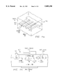
- FIGS. 1a-c are perspective and cross-sectional elevation and plan views of a first preferred embodiment vertical field effect transistor.
- FIGS. 2a-c show electrical characteristics and behavior of the first preferred embodiment.
- FIGS. 3a-d illustrate applications of the first preferred embodiment.
- FIGS. 4a-d show steps in a first preferred embodiment method of fabrication.
- FIGS. 5a-c are plan views of semiconductor substrates illustrating a step of the preferred embodiment method of fabrication.
- FIGS. 6a-b show oriented substrates and epitaxial growth.
- FIG. 7 illustrates in cross sectional view a second preferred embodiment.
- FIGS. 8a-b illustrate equipotentials of the second preferred embodiment.
- FIGS. 9a-b show electrical characteristics of the second preferred embodiment.
- FIG. 10 is a cross sectional elevation view of a third preferred embodiment.
- FIG. 11 is a perspective view of a fourth preferred embodiment.
- FIG. 12 illustrates in cross sectional view a fifth preferred embodiment.
- FIG. 13 shows in cross sectional view a sixth preferred embodiment.
- FIG. 1a shows in cutaway perspective view a first preferred embodiment vertical field effect transistor (VFET), generally denoted by the reference numeral 100, made of gallium arsenide (GaAs) and including n doped source 102, p+ doped gate 104 in the form of parallel fingers with n doped channel regions 106 between successive gate fingers, and n doped drain 108 which includes a drift region.
- FIG. 1b shows VFET 100 in cross sectional elevation view and also shows source contact 112, metal gate contact 114 which connects to gate 104 through p+ region 115, and bottom drain contact 118.
- FIG. 1a shows in cutaway perspective view a first preferred embodiment vertical field effect transistor (VFET), generally denoted by the reference numeral 100, made of gallium arsenide (GaAs) and including n doped source 102, p+ doped gate 104 in the form of parallel fingers with n doped channel regions 106 between successive gate fingers, and n doped drain 108 which includes a drift region
- FIGS. 1b-c show only seven channel regions 106 between adjacent parallel p+ regions 115; more typically there would be about 100-200 channel regions between adjacent parallel p+ regions, and the overall size of the rectangular areas surrounded by p+ 115 would be 100 ⁇ m by 200 ⁇ m.
- the use of metal gate contact 114 strapping the entire p+ region 115 lowers the gate resistance for high frequency operation.
- VFET 100 has the structure of parallel junction field effect transistors (JFETs) with current flowing vertically in FIGS. 1a-b. With a positive voltage V DS applied from drain to source, majority carrier electrons flow from source 102 through channel regions 106 to drain 108; and a voltage V GS applied to gate 104 (reverse bias of the p-n junction) controls this flow by modulating the carrier levels in channel regions 106.
- the gate length equals the channel length plus the associated p-n depletion region and is the vertical distance indicated in FIG. 1b.
- the channel opening is the distance between adjacent gate fingers as shown in FIG. 1b.
- VFET 100 has a channel length of 0.3 ⁇ m and a channel opening of 0.5 ⁇ m with a channel doping concentration of 3 ⁇ 10 16 atoms/cm 3 .
- FIG. 2a illustrates the electrical characteristics of VFET 100.
- V GS the depletion region of the p-n junction formed by gate 104 and channel 106 takes up about half of channel 106, and the drain current I D is proportional to V DS for small V DS and flows through the undepleted neutral central portion of channel 106.
- the ratio I D /V DS is called the on-resistance R ON and depends upon the channel material, geometry, doping level, substrate resistance, and contact resistance.
- the channel material resistivity equals roughly 25 micro-ohm-cm 2 for VFET 100 while for the entire VFET it is roughly 50-100 micro-ohm-cm 2 .
- V GS becomes negative and increases in magnitude, the neutral central channel portion begins to pinch off due to the reverse bias of the gate-channel junction, and the drain current pinches off.
- Power switching applications only use turned-on and turned-off states of VFET 100.
- V GS large (negative) will turn off VFET 100 and I D will be a leakage current and V DS will be large.
- the saturated current regime of pentodelike operation of a JFET will not typically be used.
- V GS -2 volts the gate-channel junction depletion regions fill up channels 106 and this allows only leakage drain current I D until V DS reaches a certain minimum value (the blocking voltage). Further increases in V DS beyond the blocking voltge cause a rapid increase in drain current.
- the drain current follows a space charge limited dependence on V DS and thus VFET 100 exhibits triodelike operation.
- increases the blocking voltage, and the ratio of blocking voltage to
- VFET 100 has a DC blocking gain of roughly 3 to 20 for V DS in the range of 5 to 50 volts.
- FIGS. 2b-c heuristically illustrate the channel carrier concentrations as a percentage of the undepleted channel carrier concentration for V GS equal to -3 volts and with V DS below the blocking voltage and above the blocking voltage, respectively.
- VFET 100 provides high frequency switching by low gate capacitance and low gate resistance through high gate doping levels and low channel doping levels plus small gate dimensions.
- FIG. 3a heuristically shows multiple VFET 100s with their drains all connected to a power supply V DD at +5 volts, with their sources connected to various devices 301, 302, . . . 310, and with their gates driven by controller 320.
- controller 320 controls the power supply to each of devices 301, 302, . . . 310.
- controller 320 has charge pump 330 to provide -3 volts. Both controller 320 and charge pump 330 could be CMOS circuits.
- FIG. 3a heuristically shows multiple VFET 100s with their drains all connected to a power supply V DD at +5 volts, with their sources connected to various devices 301, 302, . . . 310, and with their gates driven by controller 320.
- controller 320 controls the power supply to each of devices 301, 30
- 3a could be employed in battery powered systems such as portable computers where the devices 301, 302, . . . 310 would be items such as disk drives, keyboards, screens, CPUs, modems, and so forth with controller software controlled and interrupt driven to turn off all items not in use but quickly turn on items upon demand for use.
- Such power management will extend the charge life of a battery operating the portable computer, and the low voltage levels (e.g., down to 3.3 or even 1.5 volts) require a low R ON plus the high CPU frequencies (50 MHz) require rapid power switching.
- FIG. 3b shows a preferred embodiment switching voltage regulator including p-channel FET 340, lowpass filter made of inductor 342 and capacitor 344, free-wheeling diode 346, VFET 100, and pulse width modulator plus controller 348.
- This regulator has the "buck" topology and basically operates as follows. Controller 348 switches FET 340 at a fixed frequency (e.g., 100 KHz) and senses the output voltage to control the duty cycle of the switching of FET 340; this feedback sets the output DC voltage.
- the lowpass filter filters the resulting square wave from FET 340 to produce a ripple free DC output.
- Controller 348 includes a charge pump to generate negative gate voltage for VFET 100 and turns on VFET 100 when FET 340 is turned off; thus VFET 100 provides a low resistance path to ground and prevents the output node of FET 340 from going negative during the portion of the switching cycle in which FET 340 is turned off.
- Free-wheeling diode 346 parallels VFET 100 and provides the same function; however, free-wheeling diode 346 would cause a diode voltage drop, and without VFET 100 the average output DC current would pass through free-wheeling diode to cause power losses.
- VFET 100 provides a lower resistance path for the average DC current and eliminates the diode voltage drop and its attendant power losses.
- FIG. 3c illustrates a known DC-DC converter including a Schottky diode 350 for rectification.
- the converter operates in somewhat the same manner as the regulator of FIG. 3b: a pulse width modulator switches n-channel FET 352, and transformer 354 steps up (or down) the voltage of the resulting square wave.
- the lowpass filter made of inductor 356 and capacitor 358 filters the rectified square wave, and free-wheeling diode 359 prevents an overly negative filter input node.
- FIG. 3d shows a preferred embodiment DC-DC conveter with synchronous rectification by VFET 360 driven by driver 361 to be synchronized with the switching of FET 362 and with VFET 370 parallel free-wheeling diode 369.
- a preferred embodiment method of fabrication of VFET 100 for low voltage operation uses a low resistivity substrate and backside drain contact and includes the following steps:
- the MOCVD uses trimethyl gallium (or equivalent such as triethyl gallium) and arsine (or equvalent such as tertiarybutyl arsine or trimethyl arsine) plus disilane (or equivalent) for n-type doping and CCl 4 (or equvalent) for p-type doping. See FIG. 4a for a cross sectional elevation view showing substrate 402, n++ epilayer 404, n- epilayer 406, and p++ gate layer 408.
- (b) Spin on photoresist and pattern it to define 50 gate fingers 409, and then etch with an electron cyclotron resonance (ECR) chlorine-based plasma etch using the patterned photoresist as the etch mask. See FIG. 4b; the channel regions between adjacent gate fingers 409 resemble a series of parallel slots in epilayer 408.
- the gate fingers are 0.3 ⁇ m long by 0.5 ⁇ m thick by 50-100 ⁇ m wide with 0.5 ⁇ m channel openings between adjacent gate fingers.
- the gate fingers all connect to the surrounding region in p++ layer 408. Overetching removes about 0.1 ⁇ m of n- layer 406.
- the preferred embodiment method of fabrication aligns the gate sidewalls with particular crystal planes; FIGS. 5a-b and the accompanying discussion details this alignment.
- the gate finger thickness minimum depends upon the resistivity of layer 408, and the channel region opening maximum derives from the gate bias for maximum blocking voltage plus the doping level of the channel region.
- a higher breakdown voltage (about 50 volts) version of VFET 100 would use 0.7 ⁇ m channel opening with a n- doping level of 1 ⁇ 10 16 /cm 3 .
- locally trenches between gate fingers can also be viewed as gate finger pedestals on an underlying plane.
- a larger channel length would increase the blocking voltage up to breakdown limits.
- the channel length can be varied from 0.1 ⁇ m to greater than 1 ⁇ m.
- FIG. 4d Implant Be to make p++ connection 420 from etched p++ epilayer 408 to the surface of epilayer as shown in FIG. 1. (In place of the p++ implant a mesa etch down to layer 408 could be done.) Also, grow and pattern n++ epilayer 422 to make contact to n- source 412. Addition of metal contacts, encapsulation, and packaging completes a basic discrete VFET suitable for low voltage power regulation.
- FIG. 4d illustrates the essential structure.
- Metal contacts to the n+ GaAs for source and drain may be made of an alloy such as PdGeIn, AuGeNi, PdGe, TiPtAu (if layer 422 is n++ InGaAs), and so forth, and the p++ metal contact may be an alloy such as AuZn, AuBe, and AuMn.
- FIG. 5a shows a standard (100)-oriented GaAs wafer in plan view and illustrates the major and minor flats which are oriented 45° to the 010 ! and 001 ! directions and represent (011) and (01-1) oriented cleavage planes.
- An anisotropic wet etch such as H 2 SO 4 , H 2 O 2 , and H 2 O in the ratio 1:8:40 preferentially does not etch (111)Ga planes.
- a GaAs wafer subjected to an anisotropic wet etch with square etch mask leads to a raised mesa having face orientations as illustrated. Note that the wafer surface orientation tyically has a 2° tilt from precisely (100) for good growth of thick epilayers.
- gate layer 408 has gate fingers 409 formed as elongated regions parallel to either the major or minor flat of substrate 402 (see heuristic FIG. 5b in which the gate finger sidewalls are perpendicular to the plane of the Figure), then plasma etching yields gate sidewalls as ⁇ 110 ⁇ planes. These are the cleavage planes and the typical orientation.
- the in situ doping MOCVD growth from the sidewalls incorporates the silicon dopants during growth of ⁇ 110 ⁇ or higher index planes and this leads to VFETs with poor performance which may be due to the silicon (which is an amphoteric dopant) also acting as an acceptor and yielding p type channel doping or the growth on ⁇ 110 ⁇ and higher index planes creating much higher crystal defect levels than growth on ⁇ 110 ⁇ planes.
- Such an incorrect doping or high defect levels in the portion of the channel abutting the gate smears out the p-n junction or provides leakage current paths and leads to poor depletion region control and low voltage gain (or low DC blocking voltage).
- Preferred embodiment (010) or (001) orientation of the gate finger sidewalls as shown in FIG. 5c yields incorporation of the in situ silicon dopants during ⁇ 100 ⁇ plane growth and donor doping throughout the channel regions.
- the sidewalls have the same orientation as the original substrate.
- control of surface orientation to within 5° may be difficult for the sidewalls due to etch irregularities, but close to ⁇ 100 ⁇ will just be a tilted ⁇ 100 ⁇ plane and yield the proper donor silicon dopant incorporation.
- FIG. 6a illustrates in cross sectional elevation view the typical 2° tilt of the (100) orientation with atomic level terracing of a GaAs substrate for epitaxial growth.
- the atomic level terracing promotes smooth epilayer growth on a planar surface, whereas epilayer growth on untilted (100) surfaces has less uniform nucleation and yields slight ripples on the order of a few hundred angstroms in height after 1-2 ⁇ m of epilayer growth.
- the surface roughness for precise (100) oriented GaAs surfaces increases with epilayer thickness up to about 5 ⁇ m and then appears to saturate. Note that a 2° tilt with a crystal unit cell dimension of about 5.65 ⁇ yields terrace widths of roughly 100-200 ⁇ .
- step (c) for the growth in step (c) to fill the spaces between the gate fingers, the 2° tilt must be avoided.
- epitaxial growth to fill trenches and overgrow pedestals on a 2° tilted (100) surface leads to facets as illustrated in cross sectional elevation view by FIG. 6b.
- 0.7 ⁇ m thick epilayer 630 grown on substrate 600 with 0.5 ⁇ m deep and 4 ⁇ m wide trench 610 and 0.5 ⁇ m high and 4 ⁇ m wide pedestal 620 led to ledge 612 in trench 610 and ledge 622 at pedestal 620.
- the ledges For a (100) oriented substrate with a surface orientation vector tilted in the (10-1) direction the ledges also have an orientation of (10-1).
- a ledge growth in the channel regions of a VFET leads to poor performance which may arise from crystal defects due to higher index plane growth (growth on the ledges) or incorrect dopant incorporation as described in the Sidewall orientation section.
- alignment marks for aligning subsequent etch masks appear shifted in epilayer 630 due to the ledges, and this complicates the fabrication process.
- the preferred embodiment uses a precisely (100) oriented (within a tolerance of 0.5°) substrate to avoid the ledges during overgrowth. This provides uniform filing of the channel between the gate fingers and uniform doping type in the channel. The use of untilted (100) oriented substrates of the preferred embodiment also avoids alignment mark shifting.
- FIG. 7 shows in cross sectional elevation view a second preferred embodiment VFET, generally denoted by the reference numeral 700, made of GaAs and including n doped source 702, p++/p- doped layered gate 704 in the form of parallel fingers with n doped channel regions 706 between successive gate fingers, n doped drain 708 including a drift region, n+ doped source contact 710 and n+ doped drain contact 712.
- VFET 700 resembles VFET 100 except for layered gate 704 which includes alternating layers of p++ and p- dopings.
- VFET 700 has the following dimensions: gate and channel region length 0.4 ⁇ m, gate finger breadth 0.5 ⁇ m, channel region opening 0.5 ⁇ m, source length 1 ⁇ m, and drain length 1 ⁇ m.
- the n- doping level of source 702, channel regions 706, and drain 708 is about 3 ⁇ 10 16 silicon atoms/cm 3 .
- the carbon doping to make up gate 704 varies as follows with the 0.07 ⁇ m layer abutting the drain:
- Carbon dopants have a very small diffusivity in GaAs, and thus such thin layers can be fabricated by MOCVD without the dopant diffusion overwhelming the layering even upon annealing.
- FIGS. 8a-b heuristically illustrate the equipotential lines in the channel for -2 volt gate bias V GS with the drain to source voltage V DS just below blocking voltage in FIG. 8a and just above blocking voltage in FIG. 8b.
- the end p- layers reduce the corner electric field magnitude to increase the gate-to-drain breakdown voltage and reduce gate capacitance, and the middle p- layer flattens the equipotential surfaces in the channel regions and extends the high field saddle toward the drain.
- the middle p- layer could be omitted for simpler fabrication and still retain the increase in breakdown voltage; or one or both of the end p- layers could be omitted and still retain the equipotential surface flattening.
- FIGS. 9a-b show the I-V characteristics for a gate bias of -2 volts; FIG. 9a for the VFET as shown in FIG. 7 and FIG. 9b for interchanged source and drain.
- Gate 704 could include more layers, especially for longer gates, to further flatten the equipotential surfaces and improve the blocking voltage, but longer gates increase the on resistance R ON . Additionally, the gate layers could be separated by an n- layer, and then individual contacts to the gate layers could create pentodelike characteristics for the VFET.
- the layered gate could be used without the sidewall orientation or with a tilted substrate.
- a gate with doping variation along its length could be used in horizontal field effect transistors.
- a buried gate region could be a series of subregions with separate doping levels.
- FIG. 10 shows in cross sectional elevation view a third preferred embodiment VFET, generally denoted by the reference numeral 1000, made of gallium arsenide (GaAs) and including n doped source 1002, p+ doped gate 1004 in the form of parallel fingers with n doped channel regions 1006 between successive gate fingers, and n doped drain 1008.
- VFET 1000 differs from VFET 100 with respect to source/drain doping levels; in particular, VFET 1000 has lighter drain doping, as follows.
- drain 1008 leads to a higher gate/substrate breakdown voltge, reduced gate/substrate capacitance, and higher blocking voltage by effectively increasing the channel length in that the channel depletion region extends deeper into the drain. It also decreases the effect of drain-source voltage V DS changes on the gate blocking because the integrated charge is less on the substrate side.
- a channel openning of 0.8 ⁇ m with a channel doping level of 1 ⁇ 10 16 /cm 3 has about the same blocking voltage with the same gate voltage as a channel opening of 0.4 ⁇ m with a channel doping level of 3-4 ⁇ 10 16 /cm 3 ; however, the smaller channel opening with higher channel doping leads to a lower on resistance R ON .
- the p+ gate layer 1004 can also have p- layers on both source and drain sides to minimize capacitance.
- a fourth preferred embodiment VFET combines the layered gate 704 of VFET 700 with the lightly doped drain 1002 of VFET 1000.
- the fourth preferred embodiment VFET adpated for low frequency use may have the simpler layout shown in heuristic perspective view in FIG. 11.
- FIG. 11 shows p+ gate layer 1124 connected by a single doped via 1115 in a corner of the integrated circuit die to metal gate contact 1114 with all of the channels 1106 between gate fingers 1104 formed in layer 1124.
- the gate fingers are formed in repeated areas approximately 50 ⁇ m square which limits the gate finger width and gate resistance.
- the use of a single gate contact 1114 reduces the die area devoted to contacts and permits a maximal portion of gate layer 1124 to be patterned as gate fingers and channels.
- FIG. 12 shows in cross sectional elevation view a portion of fifth preferred embodiment VFET 1200 which includes source 1202, gate fingers 1204, channels 1206, and drain 1208. All of these regions are made of GaAs except gate fingers 1204 are made of 0.3 ⁇ m thick p+ GaAs sublayer 1224 plus 0.05 ⁇ m thick p+ Al 0 .3 Ga 0 .7 As sublayer 1225. The incorporation of sublayer 1225 provides a heterojunction from gate 1204 to drain 1208 and thereby increase gate-drain breakdown voltage and decrease leakage current.
- gate 1204 could be entirely p+ Al 0 .3 Ga 0 .7 As (0.3 ⁇ m thick) or be p+ Al 0 .3 Ga 0 .7 As with a thin GaAs top sublayer to aid in the n- GaAs overgrowth forming source and channels.
- the Al 0 .3 Ga 0 .7 As gate would also form a heterojunction with the channel and lessen gate-channel junction leakage.
- VFET 1200 and variants proceeds as with VFET 100 with the addition of growth of a p+ Al 0 .3 Ga 0 .7 As layer; the plasma etch to form the gate fingers also etches Al 0 .3 Ga 0 .7 As. Again, the fabrication process benefits from precise (100) orientation of the wafer and (010) and (001) orientation of the gate finger sidewalls.
- VFET 1200 could have modulated gate doping like VFET 700 and a lightly doped drain like VFET 1000.
- FIG. 13 shows in cross sectional elevation view a portion of sixth preferred embodiment heterojunction bipolar transistor (HBT) 1300 which includes n+ Al 0 .3 Ga 0 .7 As emitter 1302, p+ GaAs intrinsic base 1304, p+ extrinsic base 1306, and n- GaAs collector 1308.
- Extrinsic base 1306 has a finger structure analogous to gate fingers of VFET 100, although the number of fingers may be much smaller and the finger size larger.
- extrinsic base fingers 1306 could have a cross section of 2 ⁇ m by 2 ⁇ m to minimize the base resistance, whereas intrinsic base 1304 may have a thickness of 0.1 ⁇ m and a distance between adjacent extrinsic base fingers of 3 ⁇ m.
- Fabrication of HBT 1300 may proceed analogous to that of VFET 100 but with the n- GaAs overgrowth forming the channels and source replaced by a 0.05 ⁇ m thick growth of p+ GaAs (in situ carbon doping) to form the intrinsic base and then a 0.5 to 1.0 ⁇ m thick n+ Al 0 .3 Ga 0 .7 As (in situ silicon doping) growth to form the emitter.
- the p+ GaAs overgrowth to form the intrinsic base benefits from precise (100) orientation of the wafer to avoid any ledge beginning and the (010) and (001) orientation of the base finger sidewalls just replicates.
- n+ Al 0 .3 Ga 0 .7 As benefits from these orientations as did the n- GaAs in that the wafer orientation avoids the ledge formation and nonuniform fill of the emitter between the extrinsic base fingers and the extrinsic base sidewall orientation insures n type emitter doping.
- silicon dopants have very small diffusivities in GaAs and Al 0 .3 Ga 0 .7 As, and thus using germanium or tin in place of silicon for the n type doping to deemphasize the base sidewall orientation will generate dopant diffusion problems.
- the preferred embodiments may be varied in many ways while retaining one or more of the features of overgrowth on vertical sidewalls with approximately the same crystal plane orientation as a substrate surface, overgrowth of trenches and pedestals in untilted substrates, VFET buried gate doping varying along the gate length, and varying VFET source/drain doping.
- the dimensions of the various components could be varied, the geometry of the channels in the VFETs or the emitters in the HBTs could be varied, other III-V materials such as GaP, InP, Ga x In 1-x P, In x Ga 1-x As, AlAs, Al x Ga 1-x As, and so forth also have the zinc blende crystal structure and overgrowth properites as GaAs.
- the GaAs may be an island of material grown in a recess in a silicon wafer.
- the p++ doping by Be to make connection to the buried gates may be replaced by Zn doping; in this case metal contacts may be alloys such as TiPtAu.
- diamond and silicon carbide are possible materials for VFETs and HBTs.
- the invention has the technical advantage of better channel field control in junction field effect transistors.
Abstract
A vertical field effect transistor (700) and fabrication method with buried gates (704) having gate sidewall crystal orientation the same as the substrate surface and a low index substrate crystal orientation without tilt to a higher index direction. The gate (704) may have modulated doping along the channel (706), and the drain (708) may have a lighter doping level than the channel which may be accomplished by an epitaxial overgrowth of the gates (704) to form the channels (706).
Description
This invention was made with Government support under Contract No. N66001-91-C-6008 awarded by the Department of the Navy. The Government has certain rights in this invention.
The following applications contain subject matter related to the present application and are assigned to the assignee of the present application: application Ser. No. 07/876,252, filed Apr. 30, 1992, application Ser. No. 08/036,584, filed Mar. 24, 1993. and cofiled applications with Ser. Nos. 08/055,421, 08/056,682, and 08/056,004, now U.S. Pat. No. 5,712,189.
The invention relates to electronic semiconductor devices and circuits, and, more particularly, to vertical field effect transistors and methods of fabrication.
Various semiconductor device types have been used for power handling: junction field effect transistors (JFETs), field-controlled diodes, power metal oxide-semiconductor field effect transistors (power MOSFETs), bipolar transistors, MOS gated thyristors, and insulated gate transistor (IGT). See Baliga, Modern Power Devices ch.4 (Wiley-Interscience 1987). Power devices ideally have low forward voltage drop, high switching speed, and low control power consumption; and the vertical field effect transistors (VFET) can provide these requirements. See Sze, Physics of Semiconductor Devices p.357 (Wiley-Interscience, 2d Ed., 1981) and Campbell et al, 150 Volt Vertical Channel GaAs FET, IEDM Tech. Dig. p.258 (1982). These references show a device with parallel buried p+ gate fingers and vertical carrier flow through n type channels between the gate fingers; the bias of the gate modulates the current flow. Increased power handling may conveniently be achieved with multichannel devices. These devices may operate with unsaturated current-voltage (I-V) characteristics. The use of gallium arsenide (GaAs) rather than silicon for the semiconductor material reduces the on-resistance of such VFETs due to the higher electron mobility. See Baliga, 40 IEEE Elec.Dev.Lett. 455 (1989) and Shenai et al, Optimum semiconductors for high-power electronics, 11 IEEE Elec.Dev.Lett. 520 (1990).
Variations of the vertical FET with recessed surface gates appear in Tantraporn et al, U.S. Pat. No. 4,129,879, Frensley et al, Design and Fabrication of a GaAs Vertical MESFET, 32 IEEE Tr.Elec.Dev. 952 (1985), Campbell et al, Trapezoidal-Groove Schottky-Gate Vertical-Channel GaAs EFT (GaAs Static Induction Transistor), 6 IEEE Elec.Dev.Lett. 304 (1985), Mori et al, A High Voltage GaAs Power Static Induction Transistor, Extended Abstracts of the 19th Conference on Solid State Devices and Materials, Tokyo, 279 (1987), and Hong et al, . . . 29 Jap.J.Appl.Phys. L2427 (1990).
However, such VFETs have problems including difficulties of fabrication and enhancing performance.
The present invention provides a buried gate field effect transistor with a modulated gate doping to control channel electric fields and with channel and source doping levels greater than drain doping levels.
The drawings are schematic for clarity.
FIGS. 1a-c are perspective and cross-sectional elevation and plan views of a first preferred embodiment vertical field effect transistor.
FIGS. 2a-c show electrical characteristics and behavior of the first preferred embodiment.
FIGS. 3a-d illustrate applications of the first preferred embodiment.
FIGS. 4a-d show steps in a first preferred embodiment method of fabrication.
FIGS. 5a-c are plan views of semiconductor substrates illustrating a step of the preferred embodiment method of fabrication.
FIGS. 6a-b show oriented substrates and epitaxial growth.
FIG. 7 illustrates in cross sectional view a second preferred embodiment.
FIGS. 8a-b illustrate equipotentials of the second preferred embodiment.
FIGS. 9a-b show electrical characteristics of the second preferred embodiment.
FIG. 10 is a cross sectional elevation view of a third preferred embodiment.
FIG. 11 is a perspective view of a fourth preferred embodiment.
FIG. 12 illustrates in cross sectional view a fifth preferred embodiment.
FIG. 13 shows in cross sectional view a sixth preferred embodiment.
First preferred embodiment VFET
FIG. 1a shows in cutaway perspective view a first preferred embodiment vertical field effect transistor (VFET), generally denoted by the reference numeral 100, made of gallium arsenide (GaAs) and including n doped source 102, p+ doped gate 104 in the form of parallel fingers with n doped channel regions 106 between successive gate fingers, and n doped drain 108 which includes a drift region. FIG. 1b shows VFET 100 in cross sectional elevation view and also shows source contact 112, metal gate contact 114 which connects to gate 104 through p+ region 115, and bottom drain contact 118. FIG. 1c heuristically shows a plan view and indicates that the array of parallel gate fingers and channels can be repeated to increase total gate and channel width while retaining low gate resistance because of the gate metal around each repeated cell 150. Alternatively, the drain contact could be taken to the top surface analogous to the collector in a vertical bipolar transistor structure; this would also permit use of a high resistivity substrate and integration of other devices without a common drain. Note that for clarity FIGS. 1b-c show only seven channel regions 106 between adjacent parallel p+ regions 115; more typically there would be about 100-200 channel regions between adjacent parallel p+ regions, and the overall size of the rectangular areas surrounded by p+ 115 would be 100 μm by 200 μm. The use of metal gate contact 114 strapping the entire p+ region 115 lowers the gate resistance for high frequency operation.
FIG. 2a illustrates the electrical characteristics of VFET 100. For VGS equal to 0, the depletion region of the p-n junction formed by gate 104 and channel 106 takes up about half of channel 106, and the drain current ID is proportional to VDS for small VDS and flows through the undepleted neutral central portion of channel 106. The ratio ID /VDS is called the on-resistance RON and depends upon the channel material, geometry, doping level, substrate resistance, and contact resistance. The channel material resistivity equals roughly 25 micro-ohm-cm2 for VFET 100 while for the entire VFET it is roughly 50-100 micro-ohm-cm2.
As VGS becomes negative and increases in magnitude, the neutral central channel portion begins to pinch off due to the reverse bias of the gate-channel junction, and the drain current pinches off. This represents the standard triodelike operation of a vertical JFET. Power switching applications only use turned-on and turned-off states of VFET 100. VGS =0 (or VGS positive to forward bias the gate-channel junction for current injection) will turn on VFET 100 and ID will be large and VDS will be small; whereas, VGS large (negative) will turn off VFET 100 and ID will be a leakage current and VDS will be large. Thus the saturated current regime of pentodelike operation of a JFET will not typically be used.
With VGS =-2 volts the gate-channel junction depletion regions fill up channels 106 and this allows only leakage drain current ID until VDS reaches a certain minimum value (the blocking voltage). Further increases in VDS beyond the blocking voltge cause a rapid increase in drain current. The drain current follows a space charge limited dependence on VDS and thus VFET 100 exhibits triodelike operation. Increasing |VGS | increases the blocking voltage, and the ratio of blocking voltage to |VGS | is the DC blocking gain. VFET 100 has a DC blocking gain of roughly 3 to 20 for VDS in the range of 5 to 50 volts. Very high blocking voltages require long gates and large opening channels (large channel length to opening ratios) and reduced channel doping levels to limit the influence of VDS on the channel depletion regions and prevent the space charge limited current. Also high blocking voltages require large drains (drift regions) with low doping levels to support the large potential drop without avalanche breakdown. FIGS. 2b-c heuristically illustrate the channel carrier concentrations as a percentage of the undepleted channel carrier concentration for VGS equal to -3 volts and with VDS below the blocking voltage and above the blocking voltage, respectively.
VFET applications
FIG. 3b shows a preferred embodiment switching voltage regulator including p-channel FET 340, lowpass filter made of inductor 342 and capacitor 344, free-wheeling diode 346, VFET 100, and pulse width modulator plus controller 348. This regulator has the "buck" topology and basically operates as follows. Controller 348 switches FET 340 at a fixed frequency (e.g., 100 KHz) and senses the output voltage to control the duty cycle of the switching of FET 340; this feedback sets the output DC voltage. The lowpass filter filters the resulting square wave from FET 340 to produce a ripple free DC output. Controller 348 includes a charge pump to generate negative gate voltage for VFET 100 and turns on VFET 100 when FET 340 is turned off; thus VFET 100 provides a low resistance path to ground and prevents the output node of FET 340 from going negative during the portion of the switching cycle in which FET 340 is turned off. Free-wheeling diode 346 parallels VFET 100 and provides the same function; however, free-wheeling diode 346 would cause a diode voltage drop, and without VFET 100 the average output DC current would pass through free-wheeling diode to cause power losses. VFET 100 provides a lower resistance path for the average DC current and eliminates the diode voltage drop and its attendant power losses.
FIG. 3c illustrates a known DC-DC converter including a Schottky diode 350 for rectification. The converter operates in somewhat the same manner as the regulator of FIG. 3b: a pulse width modulator switches n-channel FET 352, and transformer 354 steps up (or down) the voltage of the resulting square wave. The lowpass filter made of inductor 356 and capacitor 358 filters the rectified square wave, and free-wheeling diode 359 prevents an overly negative filter input node. FIG. 3d shows a preferred embodiment DC-DC conveter with synchronous rectification by VFET 360 driven by driver 361 to be synchronized with the switching of FET 362 and with VFET 370 parallel free-wheeling diode 369. The converter of FIG. 3d operates analogous to the converter of FIG. 3c but with rectifying diode 350 replaced by the synchronous VFET 360 to avoid the diode voltage drop and attendant power losses and also with VFET 370 providing a low resistance path parallel free-wheeling diode 369 (analog of diode 359) to avoid its power losses.
First preferred embodiment method of fabrication
A preferred embodiment method of fabrication of VFET 100 for low voltage operation (a blocking voltage of 20 volts for a gate-to-source bias of -3 volts) uses a low resistivity substrate and backside drain contact and includes the following steps:
(a) Begin with a 25-mil thick (100)-oriented (to ±0.5°) GaAs wafer n++ doped with silicon to a level of about 2-4×10¹⁸ atoms/cm3. The substrate has true (100) orientation and does not have an orientation tilted 2° from (100) as is typically done to insure smoother epitaxial layer growth. Epitaxially grow by metalorganic chemical vapor deposition (MOCVD) the following layers of GaAs:
______________________________________
Thickness   Doping type
                      Atomic concentration
______________________________________
1.0 μm   n++       2 × 10.sup.18 /cm.sup.3
1.0 μm   n-        3 × 10.sup.16 /cm.sup.3
0.3 μm   p++       1 × 10.sup.20 /cm.sup.3
______________________________________
The MOCVD uses trimethyl gallium (or equivalent such as triethyl gallium) and arsine (or equvalent such as tertiarybutyl arsine or trimethyl arsine) plus disilane (or equivalent) for n-type doping and CCl4 (or equvalent) for p-type doping. See FIG. 4a for a cross sectional elevation view showing substrate 402, n++ epilayer 404, n- epilayer 406, and p++ gate layer 408.
(b) Spin on photoresist and pattern it to define 50 gate fingers 409, and then etch with an electron cyclotron resonance (ECR) chlorine-based plasma etch using the patterned photoresist as the etch mask. See FIG. 4b; the channel regions between adjacent gate fingers 409 resemble a series of parallel slots in epilayer 408. The gate fingers are 0.3 μm long by 0.5 μm thick by 50-100 μm wide with 0.5 μm channel openings between adjacent gate fingers. The gate fingers all connect to the surrounding region in p++ layer 408. Overetching removes about 0.1 μm of n- layer 406. The preferred embodiment method of fabrication aligns the gate sidewalls with particular crystal planes; FIGS. 5a-b and the accompanying discussion details this alignment. The gate finger thickness minimum depends upon the resistivity of layer 408, and the channel region opening maximum derives from the gate bias for maximum blocking voltage plus the doping level of the channel region. A higher breakdown voltage (about 50 volts) version of VFET 100 would use 0.7 μm channel opening with a n- doping level of 1×10¹⁶ /cm3. Note that locally trenches between gate fingers can also be viewed as gate finger pedestals on an underlying plane. A larger channel length would increase the blocking voltage up to breakdown limits. The channel length can be varied from 0.1 μm to greater than 1 μm.
(c) Epitaxially grow an n- GaAs layer both to fill the spaces (channel regions 410) between the gate fingers and to continue to form source 412 of thickness 1.0 μm. The spaces between the gate fingers fill by growth both from the bottom of the spaces (layer 406) and from the vertical sidewalls. Of course, growth from the top of layer 408 occurs during this filling, and the pattern of the gate fingers is lost and the surface becomes essentially planar after about 0.5 μm due to the on-axis orientation. The epilayer has in situ doping with silicon to a level of 3×10¹⁶ atoms/cm3. See FIG. 4c. The lack of tilt in the orientation of substrate 402 affects the quality of the interface between the original gate sidewalls and the channel region filling newly grown GaAs material. FIGS. 6a-b and the accompanying discussion below indicate the tilt effect.
(d) Implant Be to make p++ connection 420 from etched p++ epilayer 408 to the surface of epilayer as shown in FIG. 1. (In place of the p++ implant a mesa etch down to layer 408 could be done.) Also, grow and pattern n++ epilayer 422 to make contact to n- source 412. Addition of metal contacts, encapsulation, and packaging completes a basic discrete VFET suitable for low voltage power regulation. FIG. 4d illustrates the essential structure. Metal contacts to the n+ GaAs for source and drain may be made of an alloy such as PdGeIn, AuGeNi, PdGe, TiPtAu (if layer 422 is n++ InGaAs), and so forth, and the p++ metal contact may be an alloy such as AuZn, AuBe, and AuMn.
Gate orientation
FIG. 5a shows a standard (100)-oriented GaAs wafer in plan view and illustrates the major and minor flats which are oriented 45° to the 010 ! and 001 ! directions and represent (011) and (01-1) oriented cleavage planes. An anisotropic wet etch such as H2 SO4, H2 O2, and H2 O in the ratio 1:8:40 preferentially does not etch (111)Ga planes. Thus a GaAs wafer subjected to an anisotropic wet etch with square etch mask leads to a raised mesa having face orientations as illustrated. Note that the wafer surface orientation tyically has a 2° tilt from precisely (100) for good growth of thick epilayers.
When gate layer 408 has gate fingers 409 formed as elongated regions parallel to either the major or minor flat of substrate 402 (see heuristic FIG. 5b in which the gate finger sidewalls are perpendicular to the plane of the Figure), then plasma etching yields gate sidewalls as {110} planes. These are the cleavage planes and the typical orientation. However, with this orientation for the gate finger sidewalls, the in situ doping MOCVD growth from the sidewalls incorporates the silicon dopants during growth of {110} or higher index planes and this leads to VFETs with poor performance which may be due to the silicon (which is an amphoteric dopant) also acting as an acceptor and yielding p type channel doping or the growth on {110} and higher index planes creating much higher crystal defect levels than growth on {110} planes. Such an incorrect doping or high defect levels in the portion of the channel abutting the gate smears out the p-n junction or provides leakage current paths and leads to poor depletion region control and low voltage gain (or low DC blocking voltage).
Preferred embodiment (010) or (001) orientation of the gate finger sidewalls as shown in FIG. 5c yields incorporation of the in situ silicon dopants during {100} plane growth and donor doping throughout the channel regions. In effect, the sidewalls have the same orientation as the original substrate. Of course, control of surface orientation to within 5° may be difficult for the sidewalls due to etch irregularities, but close to {100} will just be a tilted {100} plane and yield the proper donor silicon dopant incorporation.
Substrate tilt
FIG. 6a illustrates in cross sectional elevation view the typical 2° tilt of the (100) orientation with atomic level terracing of a GaAs substrate for epitaxial growth. The atomic level terracing promotes smooth epilayer growth on a planar surface, whereas epilayer growth on untilted (100) surfaces has less uniform nucleation and yields slight ripples on the order of a few hundred angstroms in height after 1-2 μm of epilayer growth. The surface roughness for precise (100) oriented GaAs surfaces increases with epilayer thickness up to about 5 μm and then appears to saturate. Note that a 2° tilt with a crystal unit cell dimension of about 5.65 Å yields terrace widths of roughly 100-200 Å.
However, for the growth in step (c) to fill the spaces between the gate fingers, the 2° tilt must be avoided. In fact, it has been found that epitaxial growth to fill trenches and overgrow pedestals on a 2° tilted (100) surface leads to facets as illustrated in cross sectional elevation view by FIG. 6b. In particular, 0.7 μm thick epilayer 630 grown on substrate 600 with 0.5 μm deep and 4 μm wide trench 610 and 0.5 μm high and 4 μm wide pedestal 620 (both having sidewalls with essentially (100) orientation as described in the preceding section) led to ledge 612 in trench 610 and ledge 622 at pedestal 620. For a (100) oriented substrate with a surface orientation vector tilted in the (10-1) direction the ledges also have an orientation of (10-1). A ledge growth in the channel regions of a VFET leads to poor performance which may arise from crystal defects due to higher index plane growth (growth on the ledges) or incorrect dopant incorporation as described in the Sidewall orientation section. Also, alignment marks (trenches or pedestals) for aligning subsequent etch masks appear shifted in epilayer 630 due to the ledges, and this complicates the fabrication process.
Consequently, the preferred embodiment uses a precisely (100) oriented (within a tolerance of 0.5°) substrate to avoid the ledges during overgrowth. This provides uniform filing of the channel between the gate fingers and uniform doping type in the channel. The use of untilted (100) oriented substrates of the preferred embodiment also avoids alignment mark shifting.
Second preferred embodiment VFET
FIG. 7 shows in cross sectional elevation view a second preferred embodiment VFET, generally denoted by the reference numeral 700, made of GaAs and including n doped source 702, p++/p- doped layered gate 704 in the form of parallel fingers with n doped channel regions 706 between successive gate fingers, n doped drain 708 including a drift region, n+ doped source contact 710 and n+ doped drain contact 712. VFET 700 resembles VFET 100 except for layered gate 704 which includes alternating layers of p++ and p- dopings. VFET 700 has the following dimensions: gate and channel region length 0.4 μm, gate finger breadth 0.5 μm, channel region opening 0.5 μm, source length 1 μm, and drain length 1 μm. The n- doping level of source 702, channel regions 706, and drain 708 is about 3×10¹⁶ silicon atoms/cm3. The carbon doping to make up gate 704 varies as follows with the 0.07 μm layer abutting the drain:
______________________________________
Thickness   Doping type
                      Atomic concentration
______________________________________
0.07 μm  p-        1 × 10.sup.14 /cm.sup.3
 0.1 μm  p++       1 × 10.sup.20 /cm.sup.3
 0.1 μm  p-        1 × 10.sup.14 /cm.sup.3
 0.1 μm  p++       1 × 10.sup.20 /cm.sup.3
0.05 μm  p-        1 × 10.sup.14 /cm.sup.3
______________________________________
Carbon dopants have a very small diffusivity in GaAs, and thus such thin layers can be fabricated by MOCVD without the dopant diffusion overwhelming the layering even upon annealing.
The layering of gate 704 along its length provides both low electric fields in channel regions 706 when no gate bias is applied (so the on-resistance RON is low) and high electric fields with a reverse gate bias to have high blocking voltages and large blocking gain. FIGS. 8a-b heuristically illustrate the equipotential lines in the channel for -2 volt gate bias VGS with the drain to source voltage VDS just below blocking voltage in FIG. 8a and just above blocking voltage in FIG. 8b. The end p- layers reduce the corner electric field magnitude to increase the gate-to-drain breakdown voltage and reduce gate capacitance, and the middle p- layer flattens the equipotential surfaces in the channel regions and extends the high field saddle toward the drain. This flatter equipotential insures better drain potential blocking. Of course, the middle p- layer could be omitted for simpler fabrication and still retain the increase in breakdown voltage; or one or both of the end p- layers could be omitted and still retain the equipotential surface flattening.
FIGS. 9a-b show the I-V characteristics for a gate bias of -2 volts; FIG. 9a for the VFET as shown in FIG. 7 and FIG. 9b for interchanged source and drain.
Furthermore, the layered gate could be used without the sidewall orientation or with a tilted substrate. Lastly, a gate with doping variation along its length could be used in horizontal field effect transistors. In such a horizontal case, a buried gate region could be a series of subregions with separate doping levels.
Third preferred embodiment VFET
FIG. 10 shows in cross sectional elevation view a third preferred embodiment VFET, generally denoted by the reference numeral 1000, made of gallium arsenide (GaAs) and including n doped source 1002, p+ doped gate 1004 in the form of parallel fingers with n doped channel regions 1006 between successive gate fingers, and n doped drain 1008. VFET 1000 differs from VFET 100 with respect to source/drain doping levels; in particular, VFET 1000 has lighter drain doping, as follows.
______________________________________
Region      Doping type
                      Atomic concentration
______________________________________
Source      n-        3 × 10.sup.16 /cm.sup.3
Channel     n-        3 × 10.sup.16 /cm.sup.3
Drain       n-        1 × 10.sup.16 /cm.sup.3
______________________________________
The lighter doping of drain 1008 leads to a higher gate/substrate breakdown voltge, reduced gate/substrate capacitance, and higher blocking voltage by effectively increasing the channel length in that the channel depletion region extends deeper into the drain. It also decreases the effect of drain-source voltage VDS changes on the gate blocking because the integrated charge is less on the substrate side. Further, a channel openning of 0.8 μm with a channel doping level of 1×10¹⁶ /cm3 has about the same blocking voltage with the same gate voltage as a channel opening of 0.4 μm with a channel doping level of 3-4×10¹⁶ /cm3 ; however, the smaller channel opening with higher channel doping leads to a lower on resistance RON. Thus the difference in channel and drain doping levels yields VFETs with better performance. The p+ gate layer 1004 can also have p- layers on both source and drain sides to minimize capacitance.
Fourth preferred embodiment VFET
A fourth preferred embodiment VFET combines the layered gate 704 of VFET 700 with the lightly doped drain 1002 of VFET 1000. And the fourth preferred embodiment VFET adpated for low frequency use may have the simpler layout shown in heuristic perspective view in FIG. 11. FIG. 11 shows p+ gate layer 1124 connected by a single doped via 1115 in a corner of the integrated circuit die to metal gate contact 1114 with all of the channels 1106 between gate fingers 1104 formed in layer 1124. The gate fingers are formed in repeated areas approximately 50 μm square which limits the gate finger width and gate resistance. The use of a single gate contact 1114 reduces the die area devoted to contacts and permits a maximal portion of gate layer 1124 to be patterned as gate fingers and channels.
Heterostructure VFET and HBT
FIG. 12 shows in cross sectional elevation view a portion of fifth preferred embodiment VFET 1200 which includes source 1202, gate fingers 1204, channels 1206, and drain 1208. All of these regions are made of GaAs except gate fingers 1204 are made of 0.3 μm thick p+ GaAs sublayer 1224 plus 0.05 μm thick p+ Al0.3 Ga0.7 As sublayer 1225. The incorporation of sublayer 1225 provides a heterojunction from gate 1204 to drain 1208 and thereby increase gate-drain breakdown voltage and decrease leakage current.
Alternatively, gate 1204 could be entirely p+ Al0.3 Ga0.7 As (0.3 μm thick) or be p+ Al0.3 Ga0.7 As with a thin GaAs top sublayer to aid in the n- GaAs overgrowth forming source and channels. The Al0.3 Ga0.7 As gate would also form a heterojunction with the channel and lessen gate-channel junction leakage.
Fabrication of VFET 1200 and variants proceeds as with VFET 100 with the addition of growth of a p+ Al0.3 Ga0.7 As layer; the plasma etch to form the gate fingers also etches Al0.3 Ga0.7 As. Again, the fabrication process benefits from precise (100) orientation of the wafer and (010) and (001) orientation of the gate finger sidewalls. Of course, VFET 1200 could have modulated gate doping like VFET 700 and a lightly doped drain like VFET 1000.
FIG. 13 shows in cross sectional elevation view a portion of sixth preferred embodiment heterojunction bipolar transistor (HBT) 1300 which includes n+ Al0.3 Ga0.7 As emitter 1302, p+ GaAs intrinsic base 1304, p+ extrinsic base 1306, and n- GaAs collector 1308. Extrinsic base 1306 has a finger structure analogous to gate fingers of VFET 100, although the number of fingers may be much smaller and the finger size larger. In particular, extrinsic base fingers 1306 could have a cross section of 2 μm by 2 μm to minimize the base resistance, whereas intrinsic base 1304 may have a thickness of 0.1 μm and a distance between adjacent extrinsic base fingers of 3 μm.
Fabrication of HBT 1300 may proceed analogous to that of VFET 100 but with the n- GaAs overgrowth forming the channels and source replaced by a 0.05 μm thick growth of p+ GaAs (in situ carbon doping) to form the intrinsic base and then a 0.5 to 1.0 μm thick n+ Al0.3 Ga0.7 As (in situ silicon doping) growth to form the emitter. The p+ GaAs overgrowth to form the intrinsic base benefits from precise (100) orientation of the wafer to avoid any ledge beginning and the (010) and (001) orientation of the base finger sidewalls just replicates. The overgrowth of n+ Al0.3 Ga0.7 As benefits from these orientations as did the n- GaAs in that the wafer orientation avoids the ledge formation and nonuniform fill of the emitter between the extrinsic base fingers and the extrinsic base sidewall orientation insures n type emitter doping. Note that silicon dopants have very small diffusivities in GaAs and Al0.3 Ga0.7 As, and thus using germanium or tin in place of silicon for the n type doping to deemphasize the base sidewall orientation will generate dopant diffusion problems.
Modifications and advantages
The preferred embodiments may be varied in many ways while retaining one or more of the features of overgrowth on vertical sidewalls with approximately the same crystal plane orientation as a substrate surface, overgrowth of trenches and pedestals in untilted substrates, VFET buried gate doping varying along the gate length, and varying VFET source/drain doping.
For example, the dimensions of the various components could be varied, the geometry of the channels in the VFETs or the emitters in the HBTs could be varied, other III-V materials such as GaP, InP, Gax In1-x P, Inx Ga1-x As, AlAs, Alx Ga1-x As, and so forth also have the zinc blende crystal structure and overgrowth properites as GaAs. The GaAs may be an island of material grown in a recess in a silicon wafer. The p++ doping by Be to make connection to the buried gates may be replaced by Zn doping; in this case metal contacts may be alloys such as TiPtAu. Also, diamond and silicon carbide are possible materials for VFETs and HBTs.
The invention has the technical advantage of better channel field control in junction field effect transistors.
Claims (15)
1. A field effect transistor, comprising:
(a) a source region in a semiconductor layer;
(b) a drain region in said semiconductor layer;
(c) a gate region in said semiconductor layer and between said source region and said drain region;
(d) a channel region in said semiconductor layer and between said source region and said drain region and abutting said gate region;
(d) wherein said gate region has a doping level where said gate region abuts said channel region varying in the direction from said source region to said drain region.
2. The transistor of claim 1, wherein:
(a) said gate region includes a first subregion abutting said drain and a second subregion away from said drain, wherein said first subregion has a doping level less than the doping level of said second subregion.
3. The transistor of claim 2, wherein:
(a) said layer is made of gallium arsenide;
(b) said gate region is doped p-type with carbon; and
(c) said source, drain, and channel regions are doped n-type with silicon.
4. The transistor of claim 1, wherein:
(a) carrier flow from said source region, through said channel region, and into said drain region is substantially perpendicular to a surface of said semiconductor layer.
5. The transistor of claim 4, wherein:
(a) said gate region includes a plurality of parallel fingers with portions of said channel region between successive ones of said parallel fingers.
6. The transistor of claim 5, wherein:
(a) said layer is made of gallium arsenide;
(b) said gate region is doped p-type with carbon; and
(c) said source, drain, and channel regions are doped n-type with silicon.
7. The transistor of claim 1, wherein:
(a) said gate region includes successive subregions S1, S2, . . . SK in the direction from said drain to said source with K a positive integer greater than 2, wherein the doping level of S2 differs from that of S1 and the doping level of SK-1 differs from than that of SK.
8. The transistor of claim 7, wherein:
(a) K equals 3; and
(b) the doping levels of S1 and S3 are equal and less than that of S2.
9. The transistor of claim 7, wherein:
(a) S1 and S3 are doped more heavily than S2.
10. The transistor of claim 7, wherein:
(a) K equals 5; and
(b) the doping levels of S1, S3, and S5 are less than those of S2 and S4.
11. The transistor of claim 7, wherein:
(a) said layer is made of gallium arsenide;
(b) said gate region is doped p-type with carbon; and
(c) said source region, drain region, and channel region are doped with silicon.
12. The transistor of claim 7, wherein:
(a) carrier flow from said source region, through said channel region, and into said drain region is substantially perpendicular to a surface of said semiconductor layer.
13. The transistor of claim 12, wherein:
(a) said gate region includes a plurality of parallel fingers with portions of said channel region between successive ones of said parallel fingers.
14. The transistor of claim 7, wherein:
(a) the doping type of Sj, for a j greater than 1 and less than K, is opposite the doping type of S1 and SK, whereby said gate is split into two subgates.
15. The transistor of claim 7, wherein:
(a) S1 is made of a first semiconductor material and SK is made of a second semiconductor material with a said first material having a larger bandgap than said second material.
Priority Applications (6)
| Application Number | Priority Date | Filing Date | Title |
|---|---|---|---|
| US08/056,681 US5889298A (en) | 1993-04-30 | 1993-04-30 | Vertical JFET field effect transistor |
| JP12671794A JPH07142415A (en) | 1993-04-30 | 1994-04-28 | Method of epitaxial excess growth and perpendicular form field-effect transistor |
| EP19940106664 EP0627761B1 (en) | 1993-04-30 | 1994-04-28 | Epitaxial overgrowth method and devices |
| DE1994629130 DE69429130T2 (en) | 1993-04-30 | 1994-04-28 | Epitaxial growth method and devices |
| KR1019940009248A KR100358030B1 (en) | 1993-04-30 | 1994-04-29 | Epitaxial and Growth Methods and Vertical Field Effect Devices |
| US08/485,539 US5624860A (en) | 1993-04-30 | 1995-06-07 | Vertical field effect transistor and method |
Applications Claiming Priority (1)
| Application Number | Priority Date | Filing Date | Title |
|---|---|---|---|
| US08/056,681 US5889298A (en) | 1993-04-30 | 1993-04-30 | Vertical JFET field effect transistor |
Related Child Applications (1)
| Application Number | Title | Priority Date | Filing Date |
|---|---|---|---|
| US08/485,539 Division US5624860A (en) | 1993-04-30 | 1995-06-07 | Vertical field effect transistor and method |
Publications (1)
| Publication Number | Publication Date |
|---|---|
| US5889298A true US5889298A (en) | 1999-03-30 |
Family
ID=22005954
Family Applications (2)
| Application Number | Title | Priority Date | Filing Date |
|---|---|---|---|
| US08/056,681 Expired - Lifetime US5889298A (en) | 1993-04-30 | 1993-04-30 | Vertical JFET field effect transistor |
| US08/485,539 Expired - Lifetime US5624860A (en) | 1993-04-30 | 1995-06-07 | Vertical field effect transistor and method |
Family Applications After (1)
| Application Number | Title | Priority Date | Filing Date |
|---|---|---|---|
| US08/485,539 Expired - Lifetime US5624860A (en) | 1993-04-30 | 1995-06-07 | Vertical field effect transistor and method |
Country Status (1)
| Country | Link |
|---|---|
| US (2) | US5889298A (en) |
Cited By (67)
| Publication number | Priority date | Publication date | Assignee | Title |
|---|---|---|---|---|
| US5973341A (en) * | 1998-12-14 | 1999-10-26 | Philips Electronics North America Corporation | Lateral thin-film silicon-on-insulator (SOI) JFET device |
| US20030042627A1 (en) * | 2000-12-15 | 2003-03-06 | Farrar Paul A. | Method of alignment for buried structures formed by surface transformation of empty spaces in solid state materials |
| US6633195B2 (en) * | 1999-01-22 | 2003-10-14 | Siemens Aktiengesellschaft | Hybrid power MOSFET |
| US6690040B2 (en) * | 2001-09-10 | 2004-02-10 | Agere Systems Inc. | Vertical replacement-gate junction field-effect transistor |
| US20050024179A1 (en) * | 2002-04-18 | 2005-02-03 | Rockwell Scientific Licensing, Llc | Extended E matrix integrated magnetics (MIM) core |
| US20050173726A1 (en) * | 2004-02-09 | 2005-08-11 | International Rectifier Corp. | Normally off JFET |
| DE102004018153A1 (en) * | 2004-04-08 | 2005-12-08 | Austriamicrosystems Ag | High-voltage JFET |
| US20060038650A1 (en) * | 2004-08-19 | 2006-02-23 | Rockwell Scientific Licensing, Llc | Vertical winding structures for planar magnetic switched-mode power converters |
| US20060038649A1 (en) * | 2004-08-19 | 2006-02-23 | Rockwell Scientific Licensing, Llc | Winding structure for efficient switch-mode power converters |
| US20060157804A1 (en) * | 2004-11-30 | 2006-07-20 | Matsushita Electric Industrial Co., Ltd. | Field effect transistor and method for manufacturing the same |
| US20060187684A1 (en) * | 2005-02-08 | 2006-08-24 | Sriram Chandrasekaran | Power converter employing integrated magnetics with a current multiplier rectifier and method of operating the same |
| US20060198173A1 (en) * | 2005-02-23 | 2006-09-07 | Rozman Allen F | Control circuit for a depletion mode switch and method of operating the same |
| US20060226478A1 (en) * | 2005-03-29 | 2006-10-12 | Brar Berinder P S | Semiconductor device having a lateral channel and contacts on opposing surfaces thereof |
| US20060226477A1 (en) * | 2005-03-29 | 2006-10-12 | Brar Berinder P S | Substrate driven field-effect transistor |
| US20060255360A1 (en) * | 2005-05-13 | 2006-11-16 | Brar Berinder P S | Semiconductor device having multiple lateral channels and method of forming the same |
| US20070045765A1 (en) * | 2005-08-25 | 2007-03-01 | Brar Berinder P | Semiconductor device having substrate-driven field-effect transistor and schottky diode and method of forming the same |
| US20070069286A1 (en) * | 2005-09-27 | 2007-03-29 | Brar Berinder P S | Semiconductor device having an interconnect with sloped walls and method of forming the same |
| US20070114979A1 (en) * | 2005-02-23 | 2007-05-24 | Sriram Chandrasekaran | Power converter employing a tapped inductor and integrated magnetics and method of operating the same |
| US20070185754A1 (en) * | 2006-02-07 | 2007-08-09 | Sap Ag | Task responsibility system |
| US20070187717A1 (en) * | 2005-05-13 | 2007-08-16 | Coldwatt, Inc. | Semiconductor device having reduced on-resistance and method of forming the same |
| US20070200250A1 (en) * | 2004-08-24 | 2007-08-30 | Infineon Technologies Ag | Semiconductor Device with a Semiconductor Chip Using Lead Technology and Method of Manufacturing the Same |
| US20070275515A1 (en) * | 2006-05-25 | 2007-11-29 | Texas Instruments Incorporated | Deep buried channel junction field effect transistor (DBCJFET) |
| US20070298564A1 (en) * | 2006-06-21 | 2007-12-27 | Brar Berinder P S | Vertical Field-Effect Transistor and Method of Forming the Same |
| US20070296028A1 (en) * | 2006-06-21 | 2007-12-27 | Brar Berinder P S | Vertical Field-Effect Transistor and Method of Forming the Same |
| US20080048173A1 (en) * | 2005-08-25 | 2008-02-28 | Sadaka Mariam G | Semiconductor Device Including a Lateral Field-Effect Transistor and Schottky Diode |
| US20080054874A1 (en) * | 2006-08-31 | 2008-03-06 | Sriram Chandrasekaran | Power Converter Employing Regulators with a Coupled Inductor |
| US20080130321A1 (en) * | 2006-12-01 | 2008-06-05 | Artusi Daniel A | Power converter with an adaptive controller and method of operating the same |
| US20080130322A1 (en) * | 2006-12-01 | 2008-06-05 | Artusi Daniel A | Power system with power converters having an adaptive controller |
| US20080135854A1 (en) * | 2005-03-25 | 2008-06-12 | Nichia Corporation | Field effect transistor including a group iii-v compound semiconductor layer |
| US20080150666A1 (en) * | 2005-02-23 | 2008-06-26 | Sriram Chandrasekaran | Power Converter Employing a Tapped Inductor and Integrated Magnetics and Method of Operating the Same |
| US20080232141A1 (en) * | 2006-12-01 | 2008-09-25 | Artusi Daniel A | Power System with Power Converters Having an Adaptive Controller |
| US20080315852A1 (en) * | 2007-06-19 | 2008-12-25 | Chandrasekaran Jayaraman | System and Method for Estimating Input Power for a Power Processing Circuit |
| US20090090557A1 (en) * | 2007-10-09 | 2009-04-09 | Particle Drilling Technologies, Inc. | Injection System And Method |
| US20090097290A1 (en) * | 2007-03-14 | 2009-04-16 | Sriram Chandrasekaran | Isolated Power Converter |
| US20100165667A1 (en) * | 2006-12-01 | 2010-07-01 | Artusi Daniel A | Power System with Power Converters Having an Adaptive Controller |
| US20100182806A1 (en) * | 2009-01-19 | 2010-07-22 | Paul Garrity | Controller for a Power Converter |
| US20100321958A1 (en) * | 2009-06-17 | 2010-12-23 | Antony Brinlee | Power Converter Employing a Variable Switching Frequency and a Magnetic Device with a Non-Uniform Gap |
| US20110134664A1 (en) * | 2009-12-03 | 2011-06-09 | Berghegger Ralf Schroeder Genannt | Startup Circuit and Power Converter Employing the Same |
| US20110149607A1 (en) * | 2009-12-18 | 2011-06-23 | Aaron Jungreis | Controller for a Power Converter |
| US20110182089A1 (en) * | 2010-01-22 | 2011-07-28 | Genannt Berghegger Ralf Schroeder | Controller for a Power Converter and Method of Operating the Same |
| US20110239008A1 (en) * | 2010-03-26 | 2011-09-29 | Lam Kean W | Power Adapter Having a Universal Serial Bus Hub |
| US8354678B1 (en) * | 2011-07-11 | 2013-01-15 | International Business Machines Corporation | Structure and method for forming a light detecting diode and a light emitting diode on a silicon-on-insulator wafer backside |
| US8415737B2 (en) | 2006-06-21 | 2013-04-09 | Flextronics International Usa, Inc. | Semiconductor device with a pillar region and method of forming the same |
| US8638578B2 (en) | 2009-08-14 | 2014-01-28 | Power System Technologies, Ltd. | Power converter including a charge pump employable in a power adapter |
| US8643222B2 (en) | 2009-06-17 | 2014-02-04 | Power Systems Technologies Ltd | Power adapter employing a power reducer |
| US20140087530A1 (en) * | 2011-08-04 | 2014-03-27 | Texas Instruments Incorporated | Field Controlled Diode With Positively Biased Gate |
| RU2513644C1 (en) * | 2012-12-10 | 2014-04-20 | Федеральное государственное бюджетное образовательное учреждение высшего профессионального образования "Рязанский государственный радиотехнический университет" | Semiconductor device with negative resistance (versions) |
| US8767418B2 (en) | 2010-03-17 | 2014-07-01 | Power Systems Technologies Ltd. | Control system for a power converter and method of operating the same |
| US8792256B2 (en) | 2012-01-27 | 2014-07-29 | Power Systems Technologies Ltd. | Controller for a switch and method of operating the same |
| US8792257B2 (en) | 2011-03-25 | 2014-07-29 | Power Systems Technologies, Ltd. | Power converter with reduced power dissipation |
| US9019061B2 (en) | 2009-03-31 | 2015-04-28 | Power Systems Technologies, Ltd. | Magnetic device formed with U-shaped core pieces and power converter employing the same |
| US9077248B2 (en) | 2009-06-17 | 2015-07-07 | Power Systems Technologies Ltd | Start-up circuit for a power adapter |
| US9088216B2 (en) | 2009-01-19 | 2015-07-21 | Power Systems Technologies, Ltd. | Controller for a synchronous rectifier switch |
| US9099232B2 (en) | 2012-07-16 | 2015-08-04 | Power Systems Technologies Ltd. | Magnetic device and power converter employing the same |
| US9106130B2 (en) | 2012-07-16 | 2015-08-11 | Power Systems Technologies, Inc. | Magnetic device and power converter employing the same |
| US9190898B2 (en) | 2012-07-06 | 2015-11-17 | Power Systems Technologies, Ltd | Controller for a power converter and method of operating the same |
| US9197132B2 (en) | 2006-12-01 | 2015-11-24 | Flextronics International Usa, Inc. | Power converter with an adaptive controller and method of operating the same |
| US9214264B2 (en) | 2012-07-16 | 2015-12-15 | Power Systems Technologies, Ltd. | Magnetic device and power converter employing the same |
| US9240712B2 (en) | 2012-12-13 | 2016-01-19 | Power Systems Technologies Ltd. | Controller including a common current-sense device for power switches of a power converter |
| US9246391B2 (en) | 2010-01-22 | 2016-01-26 | Power Systems Technologies Ltd. | Controller for providing a corrected signal to a sensed peak current through a circuit element of a power converter |
| US9300206B2 (en) | 2013-11-15 | 2016-03-29 | Power Systems Technologies Ltd. | Method for estimating power of a power converter |
| US9379629B2 (en) | 2012-07-16 | 2016-06-28 | Power Systems Technologies, Ltd. | Magnetic device and power converter employing the same |
| US9812580B1 (en) | 2016-09-06 | 2017-11-07 | Qualcomm Incorporated | Deep trench active device with backside body contact |
| US10230000B2 (en) | 2017-08-08 | 2019-03-12 | Globalfoundries Inc. | Vertical-transport transistors with self-aligned contacts |
| US10312151B1 (en) | 2017-11-20 | 2019-06-04 | International Business Machines Corporation | Monolithic co-integration of MOSFET and JFET for neuromorphic/cognitive circuit applications |
| US10504889B1 (en) | 2018-07-17 | 2019-12-10 | International Business Machines Corporation | Integrating a junction field effect transistor into a vertical field effect transistor |
| US10971549B2 (en) | 2018-06-26 | 2021-04-06 | International Business Machines Corporation | Semiconductor memory device having a vertical active region |
Families Citing this family (5)
| Publication number | Priority date | Publication date | Assignee | Title |
|---|---|---|---|---|
| US6083806A (en) * | 1998-07-06 | 2000-07-04 | Motorola, Inc. | Method of forming an alignment mark |
| US6630746B1 (en) | 2000-05-09 | 2003-10-07 | Motorola, Inc. | Semiconductor device and method of making the same |
| JP4744700B2 (en) * | 2001-01-29 | 2011-08-10 | 株式会社日立製作所 | Thin film semiconductor device and image display device including thin film semiconductor device |
| US6734476B2 (en) | 2001-06-14 | 2004-05-11 | Ixys Corporation | Semiconductor devices having group III-V compound layers |
| US10395988B1 (en) | 2018-04-10 | 2019-08-27 | International Business Machines Corporation | Vertical FET transistor with reduced source/drain contact resistance |
Citations (6)
| Publication number | Priority date | Publication date | Assignee | Title |
|---|---|---|---|---|
| US4470059A (en) * | 1979-01-22 | 1984-09-04 | Zaidan Hojin Handotai Kenkyu Shinkokai | Gallium arsenide static induction transistor |
| US4498093A (en) * | 1981-09-14 | 1985-02-05 | At&T Bell Laboratories | High-power III-V semiconductor device |
| US4528745A (en) * | 1982-07-13 | 1985-07-16 | Toyo Denki Seizo Kabushiki Kaisha | Method for the formation of buried gates of a semiconductor device utilizing etch and refill techniques |
| US4654679A (en) * | 1983-10-05 | 1987-03-31 | Toyo Denki Seizo Kabushiki Kaisha | Static induction thyristor with stepped-doping gate region |
| US4712122A (en) * | 1984-07-26 | 1987-12-08 | Research Development Corp. | Heterojunction gate ballistic JFET with channel thinner than Debye length |
| US5168070A (en) * | 1990-02-07 | 1992-12-01 | Forschungszentrum Julich Gmbh | Electronic component, especially a permeable base transistor |
Family Cites Families (3)
| Publication number | Priority date | Publication date | Assignee | Title |
|---|---|---|---|---|
| JPS51132779A (en) * | 1975-05-14 | 1976-11-18 | Hitachi Ltd | Production method of vertical-junction type field-effect transistor |
| US5116455A (en) * | 1991-01-24 | 1992-05-26 | Spire Corporation | Process of making strain-free, carbon-doped epitaxial layers and products so made |
| US5231037A (en) * | 1992-04-30 | 1993-07-27 | Texas Instruments Incorporated | Method of making a power VFET device using a p+ carbon doped gate layer |
-
1993
- 1993-04-30 US US08/056,681 patent/US5889298A/en not_active Expired - Lifetime
-
1995
- 1995-06-07 US US08/485,539 patent/US5624860A/en not_active Expired - Lifetime
Patent Citations (6)
| Publication number | Priority date | Publication date | Assignee | Title |
|---|---|---|---|---|
| US4470059A (en) * | 1979-01-22 | 1984-09-04 | Zaidan Hojin Handotai Kenkyu Shinkokai | Gallium arsenide static induction transistor |
| US4498093A (en) * | 1981-09-14 | 1985-02-05 | At&T Bell Laboratories | High-power III-V semiconductor device |
| US4528745A (en) * | 1982-07-13 | 1985-07-16 | Toyo Denki Seizo Kabushiki Kaisha | Method for the formation of buried gates of a semiconductor device utilizing etch and refill techniques |
| US4654679A (en) * | 1983-10-05 | 1987-03-31 | Toyo Denki Seizo Kabushiki Kaisha | Static induction thyristor with stepped-doping gate region |
| US4712122A (en) * | 1984-07-26 | 1987-12-08 | Research Development Corp. | Heterojunction gate ballistic JFET with channel thinner than Debye length |
| US5168070A (en) * | 1990-02-07 | 1992-12-01 | Forschungszentrum Julich Gmbh | Electronic component, especially a permeable base transistor |
Cited By (130)
| Publication number | Priority date | Publication date | Assignee | Title |
|---|---|---|---|---|
| US5973341A (en) * | 1998-12-14 | 1999-10-26 | Philips Electronics North America Corporation | Lateral thin-film silicon-on-insulator (SOI) JFET device |
| US6633195B2 (en) * | 1999-01-22 | 2003-10-14 | Siemens Aktiengesellschaft | Hybrid power MOSFET |
| US6841408B2 (en) | 2000-12-15 | 2005-01-11 | Micron Technology, Inc. | Method of alignment for buried structures formed by surface transformation of empty spaces in solid state materials |
| US20030042627A1 (en) * | 2000-12-15 | 2003-03-06 | Farrar Paul A. | Method of alignment for buried structures formed by surface transformation of empty spaces in solid state materials |
| US6579738B2 (en) * | 2000-12-15 | 2003-06-17 | Micron Technology, Inc. | Method of alignment for buried structures formed by surface transformation of empty spaces in solid state materials |
| US20030157780A1 (en) * | 2000-12-15 | 2003-08-21 | Farrar Paul A. | Method of alignment for buried structures formed by surface transformation of empty spaces in solid state materials |
| US20030209814A1 (en) * | 2000-12-15 | 2003-11-13 | Farrar Paul A. | Method of alignment for buried structures formed by surface transformation of empty spaces in solid state materials |
| US6949839B2 (en) | 2000-12-15 | 2005-09-27 | Micron Technology, Inc. | Aligned buried structures formed by surface transformation of empty spaces in solid state materials |
| US6815826B2 (en) | 2000-12-15 | 2004-11-09 | Micron Technology, Inc. | Alignment for buried structures formed by surface transformation of empty spaces in solid state materials |
| US20060166429A1 (en) * | 2001-09-10 | 2006-07-27 | Samir Chaudhry | Vertical replacement-gate junction field-effect transistor |
| US7033877B2 (en) | 2001-09-10 | 2006-04-25 | Agere Systems Inc. | Vertical replacement-gate junction field-effect transistor |
| US6690040B2 (en) * | 2001-09-10 | 2004-02-10 | Agere Systems Inc. | Vertical replacement-gate junction field-effect transistor |
| US20040110345A1 (en) * | 2001-09-10 | 2004-06-10 | Samir Chaudhry | Vertical replacement-gate junction field-effect transistor |
| US20100091522A1 (en) * | 2002-04-18 | 2010-04-15 | Sriram Chandrasekaran | Extended E Matrix Integrated Magnetics (MIM) Core |
| US7633369B2 (en) | 2002-04-18 | 2009-12-15 | Flextronics International Usa, Inc. | Extended E matrix integrated magnetics (MIM) core |
| US7280026B2 (en) | 2002-04-18 | 2007-10-09 | Coldwatt, Inc. | Extended E matrix integrated magnetics (MIM) core |
| US20050024179A1 (en) * | 2002-04-18 | 2005-02-03 | Rockwell Scientific Licensing, Llc | Extended E matrix integrated magnetics (MIM) core |
| US8134443B2 (en) | 2002-04-18 | 2012-03-13 | Flextronics International Usa, Inc. | Extended E matrix integrated magnetics (MIM) core |
| US7180105B2 (en) * | 2004-02-09 | 2007-02-20 | International Rectifier Corporation | Normally off JFET |
| US20050173726A1 (en) * | 2004-02-09 | 2005-08-11 | International Rectifier Corp. | Normally off JFET |
| US20080067560A1 (en) * | 2004-04-08 | 2008-03-20 | Martin Knaipp | High Voltage Depletion Layer Field Effect Transistor |
| DE102004018153B9 (en) * | 2004-04-08 | 2012-08-23 | Austriamicrosystems Ag | High-voltage junction field-effect transistor with retrograde gate well and method for its production |
| DE102004018153B4 (en) * | 2004-04-08 | 2012-06-14 | Austriamicrosystems Ag | High-voltage junction field-effect transistor with retrograde gate well and method for its production |
| DE102004018153A1 (en) * | 2004-04-08 | 2005-12-08 | Austriamicrosystems Ag | High-voltage JFET |
| US7781809B2 (en) | 2004-04-08 | 2010-08-24 | Austriamicrosystems Ag | High voltage depletion layer field effect transistor |
| US7554430B2 (en) | 2004-08-19 | 2009-06-30 | Flextronics International Usa, Inc. | Vertical winding structures for planar magnetic switched-mode power converters |
| US7321283B2 (en) | 2004-08-19 | 2008-01-22 | Coldwatt, Inc. | Vertical winding structures for planar magnetic switched-mode power converters |
| US20060038650A1 (en) * | 2004-08-19 | 2006-02-23 | Rockwell Scientific Licensing, Llc | Vertical winding structures for planar magnetic switched-mode power converters |
| US7427910B2 (en) | 2004-08-19 | 2008-09-23 | Coldwatt, Inc. | Winding structure for efficient switch-mode power converters |
| US20080111657A1 (en) * | 2004-08-19 | 2008-05-15 | Vivek Mehrotra | Vertical Winding Structures for Planar Magnetic Switched-Mode Power Converters |
| US20060038649A1 (en) * | 2004-08-19 | 2006-02-23 | Rockwell Scientific Licensing, Llc | Winding structure for efficient switch-mode power converters |
| US20070200250A1 (en) * | 2004-08-24 | 2007-08-30 | Infineon Technologies Ag | Semiconductor Device with a Semiconductor Chip Using Lead Technology and Method of Manufacturing the Same |
| US7656033B2 (en) * | 2004-08-24 | 2010-02-02 | Infineon Technologies Ag | Semiconductor device with a semiconductor chip using lead technology and method of manufacturing the same |
| US7439595B2 (en) * | 2004-11-30 | 2008-10-21 | Matsushita Electric Industrial Co., Ltd. | Field effect transistor having vertical channel structure |
| US20060157804A1 (en) * | 2004-11-30 | 2006-07-20 | Matsushita Electric Industrial Co., Ltd. | Field effect transistor and method for manufacturing the same |
| US7417875B2 (en) | 2005-02-08 | 2008-08-26 | Coldwatt, Inc. | Power converter employing integrated magnetics with a current multiplier rectifier and method of operating the same |
| US7675764B2 (en) | 2005-02-08 | 2010-03-09 | Flextronics International Usa, Inc. | Power converter employing integrated magnetics with a current multiplier rectifier and method of operating the same |
| US20060187684A1 (en) * | 2005-02-08 | 2006-08-24 | Sriram Chandrasekaran | Power converter employing integrated magnetics with a current multiplier rectifier and method of operating the same |
| US20080150666A1 (en) * | 2005-02-23 | 2008-06-26 | Sriram Chandrasekaran | Power Converter Employing a Tapped Inductor and Integrated Magnetics and Method of Operating the Same |
| US20060198173A1 (en) * | 2005-02-23 | 2006-09-07 | Rozman Allen F | Control circuit for a depletion mode switch and method of operating the same |
| US7298118B2 (en) | 2005-02-23 | 2007-11-20 | Coldwatt, Inc. | Power converter employing a tapped inductor and integrated magnetics and method of operating the same |
| US20070114979A1 (en) * | 2005-02-23 | 2007-05-24 | Sriram Chandrasekaran | Power converter employing a tapped inductor and integrated magnetics and method of operating the same |
| US7876191B2 (en) | 2005-02-23 | 2011-01-25 | Flextronics International Usa, Inc. | Power converter employing a tapped inductor and integrated magnetics and method of operating the same |
| US7385375B2 (en) | 2005-02-23 | 2008-06-10 | Coldwatt, Inc. | Control circuit for a depletion mode switch and method of operating the same |
| US20080135854A1 (en) * | 2005-03-25 | 2008-06-12 | Nichia Corporation | Field effect transistor including a group iii-v compound semiconductor layer |
| US7560752B2 (en) * | 2005-03-25 | 2009-07-14 | Nichia Corporation | Field effect transistor including two group III-V compound semiconductor layers |
| US20060226478A1 (en) * | 2005-03-29 | 2006-10-12 | Brar Berinder P S | Semiconductor device having a lateral channel and contacts on opposing surfaces thereof |
| US20060226477A1 (en) * | 2005-03-29 | 2006-10-12 | Brar Berinder P S | Substrate driven field-effect transistor |
| US7439556B2 (en) | 2005-03-29 | 2008-10-21 | Coldwatt, Inc. | Substrate driven field-effect transistor |
| US7439557B2 (en) | 2005-03-29 | 2008-10-21 | Coldwatt, Inc. | Semiconductor device having a lateral channel and contacts on opposing surfaces thereof |
| US20070145417A1 (en) * | 2005-03-29 | 2007-06-28 | Brar Berinder P S | High voltage semiconductor device having a lateral channel and enhanced gate-to-drain separation |
| US20060255360A1 (en) * | 2005-05-13 | 2006-11-16 | Brar Berinder P S | Semiconductor device having multiple lateral channels and method of forming the same |
| US7675090B2 (en) | 2005-05-13 | 2010-03-09 | Flextronics International Usa, Inc. | Semiconductor device having a contact on a buffer layer thereof and method of forming the same |
| US7339208B2 (en) | 2005-05-13 | 2008-03-04 | Coldwatt, Inc. | Semiconductor device having multiple lateral channels and method of forming the same |
| US7838905B2 (en) | 2005-05-13 | 2010-11-23 | Flextronics International Usa, Inc. | Semiconductor device having multiple lateral channels and method of forming the same |
| US20070187717A1 (en) * | 2005-05-13 | 2007-08-16 | Coldwatt, Inc. | Semiconductor device having reduced on-resistance and method of forming the same |
| US20080054304A1 (en) * | 2005-08-25 | 2008-03-06 | Sadaka Mariam G | Semiconductor Device Including a Lateral Field-Effect Transistor and Schottky Diode |
| US20080048173A1 (en) * | 2005-08-25 | 2008-02-28 | Sadaka Mariam G | Semiconductor Device Including a Lateral Field-Effect Transistor and Schottky Diode |
| US7655963B2 (en) | 2005-08-25 | 2010-02-02 | Flextronics International Usa, Inc. | Semiconductor device including a lateral field-effect transistor and Schottky diode |
| US7642568B2 (en) | 2005-08-25 | 2010-01-05 | Flextronics International Usa, Inc. | Semiconductor device having substrate-driven field-effect transistor and Schottky diode and method of forming the same |
| US20070045765A1 (en) * | 2005-08-25 | 2007-03-01 | Brar Berinder P | Semiconductor device having substrate-driven field-effect transistor and schottky diode and method of forming the same |
| US7504673B2 (en) | 2005-08-25 | 2009-03-17 | Flextronics International Usa, Inc. | Semiconductor device including a lateral field-effect transistor and Schottky diode |
| US20080048219A1 (en) * | 2005-08-25 | 2008-02-28 | Brar Berinder P S | Semiconductor Device Having Substrate-Driven Field-Effect Transistor and Schottky Diode and Method of Forming the Same |
| US7564074B2 (en) | 2005-08-25 | 2009-07-21 | Flextronics International Usa, Inc. | Semiconductor device including a lateral field-effect transistor and Schottky diode |
| US7285807B2 (en) | 2005-08-25 | 2007-10-23 | Coldwatt, Inc. | Semiconductor device having substrate-driven field-effect transistor and Schottky diode and method of forming the same |
| US20080048174A1 (en) * | 2005-08-25 | 2008-02-28 | Sadaka Mariam G | Semiconductor Device Including a Lateral Field-Effect Transistor and Schottky Diode |
| US20070069286A1 (en) * | 2005-09-27 | 2007-03-29 | Brar Berinder P S | Semiconductor device having an interconnect with sloped walls and method of forming the same |
| US7462891B2 (en) | 2005-09-27 | 2008-12-09 | Coldwatt, Inc. | Semiconductor device having an interconnect with sloped walls and method of forming the same |
| US20070185754A1 (en) * | 2006-02-07 | 2007-08-09 | Sap Ag | Task responsibility system |
| US7348228B2 (en) | 2006-05-25 | 2008-03-25 | Texas Instruments Incorporated | Deep buried channel junction field effect transistor (DBCJFET) |
| US20070275515A1 (en) * | 2006-05-25 | 2007-11-29 | Texas Instruments Incorporated | Deep buried channel junction field effect transistor (DBCJFET) |
| US7541640B2 (en) | 2006-06-21 | 2009-06-02 | Flextronics International Usa, Inc. | Vertical field-effect transistor and method of forming the same |
| US7663183B2 (en) * | 2006-06-21 | 2010-02-16 | Flextronics International Usa, Inc. | Vertical field-effect transistor and method of forming the same |
| US8415737B2 (en) | 2006-06-21 | 2013-04-09 | Flextronics International Usa, Inc. | Semiconductor device with a pillar region and method of forming the same |
| US20070298564A1 (en) * | 2006-06-21 | 2007-12-27 | Brar Berinder P S | Vertical Field-Effect Transistor and Method of Forming the Same |
| US20070296028A1 (en) * | 2006-06-21 | 2007-12-27 | Brar Berinder P S | Vertical Field-Effect Transistor and Method of Forming the Same |
| US20080054874A1 (en) * | 2006-08-31 | 2008-03-06 | Sriram Chandrasekaran | Power Converter Employing Regulators with a Coupled Inductor |
| US8125205B2 (en) | 2006-08-31 | 2012-02-28 | Flextronics International Usa, Inc. | Power converter employing regulators with a coupled inductor |
| US20080130321A1 (en) * | 2006-12-01 | 2008-06-05 | Artusi Daniel A | Power converter with an adaptive controller and method of operating the same |
| US7675758B2 (en) | 2006-12-01 | 2010-03-09 | Flextronics International Usa, Inc. | Power converter with an adaptive controller and method of operating the same |
| US7667986B2 (en) | 2006-12-01 | 2010-02-23 | Flextronics International Usa, Inc. | Power system with power converters having an adaptive controller |
| US20080232141A1 (en) * | 2006-12-01 | 2008-09-25 | Artusi Daniel A | Power System with Power Converters Having an Adaptive Controller |
| US20080130322A1 (en) * | 2006-12-01 | 2008-06-05 | Artusi Daniel A | Power system with power converters having an adaptive controller |
| US9197132B2 (en) | 2006-12-01 | 2015-11-24 | Flextronics International Usa, Inc. | Power converter with an adaptive controller and method of operating the same |
| US8477514B2 (en) | 2006-12-01 | 2013-07-02 | Flextronics International Usa, Inc. | Power system with power converters having an adaptive controller |
| US7889517B2 (en) | 2006-12-01 | 2011-02-15 | Flextronics International Usa, Inc. | Power system with power converters having an adaptive controller |
| US7675759B2 (en) | 2006-12-01 | 2010-03-09 | Flextronics International Usa, Inc. | Power system with power converters having an adaptive controller |
| US20100165667A1 (en) * | 2006-12-01 | 2010-07-01 | Artusi Daniel A | Power System with Power Converters Having an Adaptive Controller |
| US20090097290A1 (en) * | 2007-03-14 | 2009-04-16 | Sriram Chandrasekaran | Isolated Power Converter |
| US8502520B2 (en) | 2007-03-14 | 2013-08-06 | Flextronics International Usa, Inc | Isolated power converter |
| US20080315852A1 (en) * | 2007-06-19 | 2008-12-25 | Chandrasekaran Jayaraman | System and Method for Estimating Input Power for a Power Processing Circuit |
| US7906941B2 (en) | 2007-06-19 | 2011-03-15 | Flextronics International Usa, Inc. | System and method for estimating input power for a power processing circuit |
| US20090090557A1 (en) * | 2007-10-09 | 2009-04-09 | Particle Drilling Technologies, Inc. | Injection System And Method |
| US8520414B2 (en) | 2009-01-19 | 2013-08-27 | Power Systems Technologies, Ltd. | Controller for a power converter |
| US9088216B2 (en) | 2009-01-19 | 2015-07-21 | Power Systems Technologies, Ltd. | Controller for a synchronous rectifier switch |
| US20100182806A1 (en) * | 2009-01-19 | 2010-07-22 | Paul Garrity | Controller for a Power Converter |
| US9019061B2 (en) | 2009-03-31 | 2015-04-28 | Power Systems Technologies, Ltd. | Magnetic device formed with U-shaped core pieces and power converter employing the same |
| US8514593B2 (en) | 2009-06-17 | 2013-08-20 | Power Systems Technologies, Ltd. | Power converter employing a variable switching frequency and a magnetic device with a non-uniform gap |
| US8643222B2 (en) | 2009-06-17 | 2014-02-04 | Power Systems Technologies Ltd | Power adapter employing a power reducer |
| US9077248B2 (en) | 2009-06-17 | 2015-07-07 | Power Systems Technologies Ltd | Start-up circuit for a power adapter |
| US20100321958A1 (en) * | 2009-06-17 | 2010-12-23 | Antony Brinlee | Power Converter Employing a Variable Switching Frequency and a Magnetic Device with a Non-Uniform Gap |
| US8638578B2 (en) | 2009-08-14 | 2014-01-28 | Power System Technologies, Ltd. | Power converter including a charge pump employable in a power adapter |
| US20110134664A1 (en) * | 2009-12-03 | 2011-06-09 | Berghegger Ralf Schroeder Genannt | Startup Circuit and Power Converter Employing the Same |
| US8976549B2 (en) | 2009-12-03 | 2015-03-10 | Power Systems Technologies, Ltd. | Startup circuit including first and second Schmitt triggers and power converter employing the same |
| US20110149607A1 (en) * | 2009-12-18 | 2011-06-23 | Aaron Jungreis | Controller for a Power Converter |
| US8520420B2 (en) | 2009-12-18 | 2013-08-27 | Power Systems Technologies, Ltd. | Controller for modifying dead time between switches in a power converter |
| US9246391B2 (en) | 2010-01-22 | 2016-01-26 | Power Systems Technologies Ltd. | Controller for providing a corrected signal to a sensed peak current through a circuit element of a power converter |
| US8787043B2 (en) | 2010-01-22 | 2014-07-22 | Power Systems Technologies, Ltd. | Controller for a power converter and method of operating the same |
| US20110182089A1 (en) * | 2010-01-22 | 2011-07-28 | Genannt Berghegger Ralf Schroeder | Controller for a Power Converter and Method of Operating the Same |
| US8767418B2 (en) | 2010-03-17 | 2014-07-01 | Power Systems Technologies Ltd. | Control system for a power converter and method of operating the same |
| US20110239008A1 (en) * | 2010-03-26 | 2011-09-29 | Lam Kean W | Power Adapter Having a Universal Serial Bus Hub |
| US8792257B2 (en) | 2011-03-25 | 2014-07-29 | Power Systems Technologies, Ltd. | Power converter with reduced power dissipation |
| US8354678B1 (en) * | 2011-07-11 | 2013-01-15 | International Business Machines Corporation | Structure and method for forming a light detecting diode and a light emitting diode on a silicon-on-insulator wafer backside |
| US8759171B2 (en) * | 2011-08-04 | 2014-06-24 | Texas Instruments Incorporated | Field controlled diode with positively biased gate |
| US20140087530A1 (en) * | 2011-08-04 | 2014-03-27 | Texas Instruments Incorporated | Field Controlled Diode With Positively Biased Gate |
| US8792256B2 (en) | 2012-01-27 | 2014-07-29 | Power Systems Technologies Ltd. | Controller for a switch and method of operating the same |
| US9190898B2 (en) | 2012-07-06 | 2015-11-17 | Power Systems Technologies, Ltd | Controller for a power converter and method of operating the same |
| US9379629B2 (en) | 2012-07-16 | 2016-06-28 | Power Systems Technologies, Ltd. | Magnetic device and power converter employing the same |
| US9099232B2 (en) | 2012-07-16 | 2015-08-04 | Power Systems Technologies Ltd. | Magnetic device and power converter employing the same |
| US9106130B2 (en) | 2012-07-16 | 2015-08-11 | Power Systems Technologies, Inc. | Magnetic device and power converter employing the same |
| US9214264B2 (en) | 2012-07-16 | 2015-12-15 | Power Systems Technologies, Ltd. | Magnetic device and power converter employing the same |
| RU2513644C1 (en) * | 2012-12-10 | 2014-04-20 | Федеральное государственное бюджетное образовательное учреждение высшего профессионального образования "Рязанский государственный радиотехнический университет" | Semiconductor device with negative resistance (versions) |
| US9240712B2 (en) | 2012-12-13 | 2016-01-19 | Power Systems Technologies Ltd. | Controller including a common current-sense device for power switches of a power converter |
| US9300206B2 (en) | 2013-11-15 | 2016-03-29 | Power Systems Technologies Ltd. | Method for estimating power of a power converter |
| US9812580B1 (en) | 2016-09-06 | 2017-11-07 | Qualcomm Incorporated | Deep trench active device with backside body contact |
| US10230000B2 (en) | 2017-08-08 | 2019-03-12 | Globalfoundries Inc. | Vertical-transport transistors with self-aligned contacts |
| US10312151B1 (en) | 2017-11-20 | 2019-06-04 | International Business Machines Corporation | Monolithic co-integration of MOSFET and JFET for neuromorphic/cognitive circuit applications |
| US10971549B2 (en) | 2018-06-26 | 2021-04-06 | International Business Machines Corporation | Semiconductor memory device having a vertical active region |
| US10504889B1 (en) | 2018-07-17 | 2019-12-10 | International Business Machines Corporation | Integrating a junction field effect transistor into a vertical field effect transistor |
| US11011513B2 (en) | 2018-07-17 | 2021-05-18 | International Business Machines Corporation | Integrating a junction field effect transistor into a vertical field effect transistor |
Also Published As
| Publication number | Publication date |
|---|---|
| US5624860A (en) | 1997-04-29 |
Similar Documents
| Publication | Publication Date | Title |
|---|---|---|
| US5889298A (en) | Vertical JFET field effect transistor | |
| US6097046A (en) | Vertical field effect transistor and diode | |
| US5712189A (en) | Epitaxial overgrowth method | |
| US6229197B1 (en) | Epitaxial overgrowth method and devices | |
| US5554561A (en) | Epitaxial overgrowth method | |
| US5610085A (en) | Method of making a vertical FET using epitaxial overgrowth | |
| US4636823A (en) | Vertical Schottky barrier gate field-effect transistor in GaAs/GaAlAs | |
| US11081578B2 (en) | III-V depletion mode semiconductor device | |
| US4466173A (en) | Methods for fabricating vertical channel buried grid field controlled devices including field effect transistors and field controlled thyristors utilizing etch and refill techniques | |
| US5399887A (en) | Modulation doped field effect transistor | |
| EP0656646A1 (en) | Method of making devices with buried layers by epitaxial growth | |
| JPH0624208B2 (en) | Semiconductor device | |
| US5949096A (en) | Field effect transistor with stabilized threshold voltage | |
| EP0566591B1 (en) | Semiconductor device | |
| US4644381A (en) | I2 L heterostructure bipolar transistors and method of making the same | |
| EP0627761B1 (en) | Epitaxial overgrowth method and devices | |
| US4791072A (en) | Method for making a complementary device containing MODFET | |
| CN115513293A (en) | Enhanced gallium nitride heterojunction field effect transistor | |
| US6876012B2 (en) | Hetero-bipolar transistor | |
| US7208777B1 (en) | Field-effect semiconductor device | |
| JP2643890B2 (en) | Tunnel transistor | |
| US4745085A (en) | Method of making I2 L heterostructure bipolar transistors | |
| US11527619B2 (en) | Nitride-based semiconductor layer sharing between transistors | |
| KR100275496B1 (en) | Method for fabricating the heterojunction bipolar transistor | |
| US20240006498A1 (en) | Field effect transistor device |
Legal Events
| Date | Code | Title | Description |
|---|---|---|---|
| AS | Assignment |
Owner name: TEXAS INSTRUMENTS INCORPORATED, TEXAS Free format text: ASSIGNMENT OF ASSIGNORS INTEREST;ASSIGNORS:PLUMTON, DONALD L.;YUAN, HAN-TZONG;REEL/FRAME:006561/0505 Effective date: 19930430 |
|
| STPP | Information on status: patent application and granting procedure in general |
Free format text: APPLICATION UNDERGOING PREEXAM PROCESSING |
|
| FPAY | Fee payment |
Year of fee payment: 4 |
|
| FPAY | Fee payment |
Year of fee payment: 8 |
|
| FPAY | Fee payment |
Year of fee payment: 12 |