US5890217A - Coherence apparatus for cache of multiprocessor - Google Patents
Coherence apparatus for cache of multiprocessor Download PDFInfo
- Publication number
- US5890217A US5890217A US08/598,243 US59824396A US5890217A US 5890217 A US5890217 A US 5890217A US 59824396 A US59824396 A US 59824396A US 5890217 A US5890217 A US 5890217A
- Authority
- US
- United States
- Prior art keywords
- bus
- processor module
- cache
- processor
- command
- Prior art date
- Legal status (The legal status is an assumption and is not a legal conclusion. Google has not performed a legal analysis and makes no representation as to the accuracy of the status listed.)
- Expired - Lifetime
Links
- 238000003860 storage Methods 0.000 claims abstract description 274
- 230000015654 memory Effects 0.000 claims description 264
- 238000012546 transfer Methods 0.000 claims description 122
- 230000004044 response Effects 0.000 claims description 95
- 238000000034 method Methods 0.000 claims description 70
- 230000008569 process Effects 0.000 claims description 65
- 238000010276 construction Methods 0.000 claims description 29
- 230000005540 biological transmission Effects 0.000 claims description 24
- 230000005856 abnormality Effects 0.000 claims description 14
- 238000006243 chemical reaction Methods 0.000 claims description 9
- 238000001514 detection method Methods 0.000 claims description 4
- 238000010586 diagram Methods 0.000 description 45
- 238000012545 processing Methods 0.000 description 40
- 238000010926 purge Methods 0.000 description 28
- 230000006870 function Effects 0.000 description 9
- 238000009434 installation Methods 0.000 description 8
- 230000008859 change Effects 0.000 description 6
- 230000007704 transition Effects 0.000 description 5
- 230000004913 activation Effects 0.000 description 4
- 230000007246 mechanism Effects 0.000 description 3
- 238000012544 monitoring process Methods 0.000 description 3
- 230000015572 biosynthetic process Effects 0.000 description 2
- 230000001427 coherent effect Effects 0.000 description 2
- 230000014759 maintenance of location Effects 0.000 description 2
- 102100026897 Cystatin-C Human genes 0.000 description 1
- 101000912205 Homo sapiens Cystatin-C Proteins 0.000 description 1
- 230000008901 benefit Effects 0.000 description 1
- 230000001419 dependent effect Effects 0.000 description 1
- 238000011161 development Methods 0.000 description 1
- 230000006872 improvement Effects 0.000 description 1
- 230000005764 inhibitory process Effects 0.000 description 1
- 238000013507 mapping Methods 0.000 description 1
- 230000002250 progressing effect Effects 0.000 description 1
- 230000009467 reduction Effects 0.000 description 1
- 238000004092 self-diagnosis Methods 0.000 description 1
- 230000000087 stabilizing effect Effects 0.000 description 1
- 230000001360 synchronised effect Effects 0.000 description 1
- 230000001052 transient effect Effects 0.000 description 1
Images


Classifications
-
- G—PHYSICS
- G06—COMPUTING; CALCULATING OR COUNTING
- G06F—ELECTRIC DIGITAL DATA PROCESSING
- G06F12/00—Accessing, addressing or allocating within memory systems or architectures
- G06F12/02—Addressing or allocation; Relocation
- G06F12/08—Addressing or allocation; Relocation in hierarchically structured memory systems, e.g. virtual memory systems
- G06F12/0802—Addressing of a memory level in which the access to the desired data or data block requires associative addressing means, e.g. caches
- G06F12/0806—Multiuser, multiprocessor or multiprocessing cache systems
- G06F12/0815—Cache consistency protocols
- G06F12/0817—Cache consistency protocols using directory methods
-
- G—PHYSICS
- G06—COMPUTING; CALCULATING OR COUNTING
- G06F—ELECTRIC DIGITAL DATA PROCESSING
- G06F12/00—Accessing, addressing or allocating within memory systems or architectures
- G06F12/02—Addressing or allocation; Relocation
- G06F12/08—Addressing or allocation; Relocation in hierarchically structured memory systems, e.g. virtual memory systems
- G06F12/0802—Addressing of a memory level in which the access to the desired data or data block requires associative addressing means, e.g. caches
- G06F12/0806—Multiuser, multiprocessor or multiprocessing cache systems
- G06F12/0815—Cache consistency protocols
- G06F12/0831—Cache consistency protocols using a bus scheme, e.g. with bus monitoring or watching means
-
- G—PHYSICS
- G06—COMPUTING; CALCULATING OR COUNTING
- G06F—ELECTRIC DIGITAL DATA PROCESSING
- G06F2212/00—Indexing scheme relating to accessing, addressing or allocation within memory systems or architectures
- G06F2212/25—Using a specific main memory architecture
- G06F2212/254—Distributed memory
- G06F2212/2542—Non-uniform memory access [NUMA] architecture
Definitions
- the invention relates to a cache coherence apparatus for a multiprocessor system in which a plurality of processor modules are connected through a system bus and, more particularly, to a coherence apparatus for a cache of a multiprocessor system in which a plurality of processor elements with caches are connected in a processor module through a main storage and an internal common bus.
- a sole memory is not provided but local memories which function as a main storage are distributed and arranged on a unit basis for a predetermined number of processors.
- Common memory areas are distributed and arranged for a plurality of local memories and the common memories can be flexibly constructed in dependence on the number of local memory units according to a system scale.
- FIG. 1 shows a conventional typical multiprocessor system.
- the system has two processor modules 1000-1 and 1000-2.
- the processor modules 1000-1 and 1000-2 have the same construction.
- the processor module 1000-1 it is constructed by processor elements 1100-1 and 1100-2, cache units 1200-1 and 1200-2, a common bus 1300-1, and a local storage unit 1400-1.
- the processor elements 1100-1 and 1100-2 have therein primary caches and are also provided with the cache units 1200-1 and 1200-2 as secondary caches on the outside.
- the local storage unit 1400-1 functions as each main storage by allocating particular physical spaces to the processor elements 1100-1 and 1100-2.
- the local storage unit 1400-1 allocates a common memory space which is shared by all of processor elements, 1100-1 to 1100-4, of the processor modules 1000-1 and on the cache of the accessing source is updated to a 1000-2.
- the processor module 1000-2 side is also constructed by processor elements 1100-3 and 1100-4, cache units 1200-3 and 1200-4, a common bus 1300-2, and a local storage unit 1400-2.
- the common buses, 1300-1 and 1300-2, of the processor modules 1000-1 and 1000-2 operate as one bus connected via a back panel of a module casing.
- a cache control of the cache units 1200-1 to 1200-4 associated with a plurality of processor elements, 1100-1 to 1100- 4 when there is a read access in one of the processor elements and there is a mishit, a copy value of a read address is transferred to the cache by the access to the corresponding local storage.
- a copy value of the corresponding local storage is transferred to the cache and is overwritten. In this instance, the value in the main storage and the overwritten copy value in the cache are different. Therefore, a cache coherence is maintained by a copy back which transfers the newest value in the cache to the main storage and updating the old value.
- the copy values in the caches other than the cache to which the write access was performed are invalidated.
- the copy value in the cache of the accessing source is updated to a newest value and, subsequently, the newest value is copied back to the local storage, thereby maintaining the cache coherence.
- the multiprocessor system of FIG. 1 uses a construction such that all of the processor elements, cache units, and local storages are connected to one bus, there are the following problems.
- the load on the bus can be reduced by providing a plurality of common buses, when the number of processors increases to ten or twenty processors, the system cannot cope effectively with it.
- Each of the processor modules 1000-1 and 1000-2 is constructed on a module casing unit basis. Therefore, the common buses 1300-1 and 1300-2 are connected by a cable using connectors via a back panel of the casing. Thus, the line length of the bus is increased and the clock frequency of the bus cannot be raised due to electrical characteristics. For example, although the clock frequency can be set to 60 MHz in case of only one bus in the module, it is reduced to 40 MHz in case of the bus connection which shares the back panel.
- a system bus In the multiprocessor system, a system bus particularly exerts a large influence on the performance.
- the data transfer speed and the bus usage efficiency as a ratio of cycles which are used for data transfer over the total bus cycles have to be raised. Otherwise, the system bus becomes a bottleneck and even if the number of processors is increased, the performance is not improved.
- the width of data bus is widened or an interface of a small signal amplitude is used, thereby raising an operating frequency of the bus.
- a cache coherence apparatus in which by using a common bus structure of two hierarchies such that common buses are provided in a processor module and outside thereof, a cache coherence is efficiently maintained between caches of a plurality of processors built in each processor module and a local storage which functions as one distributed main storage provided for each module, thereby raising the processing performance.
- a common bus of a cache coherence apparatus in which a cache coherence is efficiently maintained and an augmentability of the system is not lost.
- the invention has a processor group having a plurality of processors.
- the processor group is divided into, for example, three processor modules having at least one or more processors therein.
- a main storage which is shared by the processor group is provided.
- the main storage is divided into a plurality of local storages.
- Each local storage is arranged on the processor module.
- each local storage is referred to as a distributed main storage.
- a cache unit to maintain the accessing speed of the distributed main storage high, is provided for each processor.
- a registration state of data of the distributed main storage to the cache unit is stored in a directory memory on a cache line unit basis.
- the distributed main storage and the cache unit are connected by a snoop bus (internal common bus).
- the processor modules are connected by a system bus (external common bus).
- a memory control module is provided for the distributed main storage of the processor module and the directory memory.
- the memory control module recognizes the distributed main storage in which the access data exists.
- the memory control module accesses it and responds.
- an access command is transmitted to an external common bus.
- the memory control module refers to the directory memory.
- the cache unit on the registration destination is accessed and a response is made.
- a cache unit on the registering destination there exists a case where it is in the module and a case where it is another processor module out of the module.
- the memory control module updates a cache state in the directory memory in accordance with the access result.
- the cache unit divides the cache line into a plurality of sublines and manages the same.
- a cache state in a "dirty" state in which the data on the cache unit has a newest value and the data on the distributed in storage has an old value is stored in the directory memory on a subline unit basis.
- a "share” state in the case where the data on the cache unit and the data in the distributed main storage are identical is stored in the directory memory on a cache line unit basis.
- the storage of the cache state in the directory memory is executed on a processor module unit basis.
- the processor module has a memory management unit to store a correspondence state with a plurality of processor modules into the directory memory and designates the registration into the directory memory on a unit basis of a plurality of processor modules.
- a memory control module of the processor module comprises: a memory management unit to manage the distributed main storage and the directory memory; a protocol management unit to manage a protocol conversion of the snoop bus and the system bus; and a module connection unit to couple the processor modules by the system bus.
- the cache unit divides the cache line of, for example, 256 bytes into sublines each consisting of 64 bytes for management purposes.
- a dirty state in which the data on the cache is the newest value and the data on the distributed main storage is the old data is registered in the directory memory on a subline unit basis.
- the share state in which the data on the cache and the data on the distributed main storage have the same value is registered on a cache line unit basis.
- a directory entry registered in the directory memory on a cache line unit basis has, for example, a plurality of subline bits D3 to D0 indicative of the presence or absence of the dirty state, and shared map bits S7 to S0 indicative of the shared state of each of the plurality of processor modules.
- a construction register to register a correspondence relation between the bit positions of the shared map bits S7 to S0 and the processor modules.
- the share state of a plurality of processor modules can be registered into the same map bit by the construction register.
- information (PM-ID) of the processor module in which the cache unit having the newest value, corresponding to the bit set is stored into a specific area of the distributed main storage.
- information (PM-ID) of the processor module in which the newest value exists is stored into a specific area of the distributed main storage.
- the processor executes a read access or write access of the cache line on a subline unit basis.
- the system bus as an external common bus
- the snoop bus as an internal common bus, transfer the information by a split form in which a command transfer and a response transfer are separated.
- the cache coherence for the read access of the processor has reading modes 1 to 3.
- the reading mode 1 relates to a case where in response to the read access of an arbitrary processor in the first processor module, a mishits occurs in the its cache unit and all of the other cache units connected by the snoop bus, the read address exists in the distributed main storage in the first processor module, and further the data of the read address exists in the dirty state in which the cache unit in the second processor module as a remote has the newest value.
- the first processor module which generated the read access generates a command to the system bus and accesses the second processor module and obtains the newest value from the cache unit in the dirty state through the its snoop bus. After that, the newest value is transmitted to the first processor module by the system bus.
- the first processor module stores the newest value obtained by the above response into the cache unit of the accessing source and allows the cache unit to respond to the read access and, at the same time, writes the newest value into the distributed main storage, thereby maintaining the cache coherence.
- the directory entry in the directory memory is updated from the dirty state to the share state and the cache unit of the accessing source updates an invalidation state of a tag memory to a share state.
- the reading mode 2 relates to the case where for the read access of an arbitrary processor in the first processor module, mishits occur in the its cache unit and all of the other cache units connected by the snoop bus, the read address exists in the distributed main storage in the second processor module, and further the data in the read address exists in the dirty state in which the cache unit in the third processor module has the newest value.
- the first processor module generates a command to the system bus and accesses the second processor module.
- the second processor module generates a command to the system bus on the basis of the command received from the system bus and accesses the third processor module.
- the third processor module obtains the newest value from the cache unit in the dirty state by the its snoop bus and, after that, transmits the newest value to the first and second processor modules by the system bus.
- the second processor module writes the newest value obtained by the response received into the distributed main storage.
- the first processor module stores the newest value obtained by response received into the cache unit of the accessing source and allows the cache unit to respond to the read access.
- the second processor module updates the directory entry of the directory memory from the "dirty" state to the "share” state.
- the cache unit of the accessing source of the first processor module updates the "invalid" state of the tag memory to the "share” state.
- Reading mode 3 maintains cache coherence between the caches in a certain processor module. Namely, reading mode 3 relates to the case where although a mishit occurs in the a processor's cache unit for the read access of an arbitrary processor in an arbitrary processor module, the newest value exists in the cache unit of another processor connected by the snoop bus. In this case, the transfer of the newest value is executed between both of the cache units through the snoop bus and the newest value is stored into the cache unit 18 of the accessing source, thereby allowing the cache unit 18 to respond to the read access. The transfer of the newest value using the snoop bus in this case is executed on a cache subline unit basis. Subsequently, the cache coherence for a write access of the processor has writing modes 1 to 5.
- the writing mode 1 relates to the case where for the write access of an arbitrary processor in the first processor module, the copy value is not stored in the its cache unit and the other cache units connected by the snoop bus in a state in which the write privilege is possessed and mishits occur, the write address exists in the distributed main storage in the first processor module, and further the copy value in the write address of the distributed main storage exists in the cache units of the other plurality of processor modules other than the first processor module in the share state.
- the first processor module generates an invalidating command to all of the processor modules in the share state by using the system bus. All of the processor modules in the share state simultaneously receive the invalidating command and independently respond to the first processor module by using the system bus when the invalidation is successful.
- the first processor module recognizes the success in invalidation by receiving all responses from the system bus and stores the copy value in the write address of the distributed main storage into the cache unit of the accessing source, thereby allowing the copy value to be overwritten by the write access.
- the share state in the directory entry of the directory memory is updated to the dirty state.
- Writing mode 2 relates to the case involving the write access of an arbitrary processor in the first processor module, the copy value is not registered in its cache unit and the other cache units connected by the snoop bus in a state in which the write privilege is possessed and mishits occur.
- the write address exists in the distributed main storage in the first processor module, and further the copy value in the write address of the distributed main storage exists in the cache units of a plurality of processor modules including the first processor module in the share state.
- simultaneous invalidating commands are generated to all of the processor modules in the share state by using the system bus, and the first processor module generates the invalidating command to the cache unit in the first processor module by using the snoop bus.
- All of the processor modules in the share state simultaneously receive the invalidating command and independently respond with an indication of success in invalidation to the first processor module by using the system bus. Simultaneously, the cache unit in the first processor module responds indicating the success in invalidation by using the snoop bus.
- the first processor module recognizes the success in invalidation by receiving all of the responses from the system bus and the response from the its snoop bus and stores the copy value in the write address of the distributed main storage into the cache unit, thereby allowing the copy value to be overwritten by the write access of the processor.
- the share state in the directory entry of the directory memory is updated to the dirty state.
- the writing mode 3 relates to the case of the write access of the processor in the first processor module, the copy value is not registered in the its cache unit and the other cache units connected through the snoop bus in a state in which the write privilege is possessed and mishits occur, the write address exists in the distributed main storage in the second processor module, and further the copy value in the write address of the distributed main storage exists in the cache units of a plurality of processor modules other than the second processor module in the share state.
- the first processor module generates a request command (home command) of the write privilege to the second processor module by using the system bus.
- the second processor module which received the request command of the write privilege generates the invalidating command (purge command) to all of the other processor modules in the share state by using the system bus.
- All of the processor modules in the share state simultaneously receive the invalidating command and independently respond to the second processor module by using the system bus to indicate that the invalidation was successful.
- the second processor module transmits the write privilege including the copy value in the access address of the its distributed main storage to the first processor module by using the system bus.
- the first processor module stores the copy value obtained by the reception of the response of the write privilege into the cache unit of the accessing source, thereby allowing the copy value to be overwritten by the write access of the processor.
- the second processor module updates the share state in the directory entry of the self directory memory to the dirty state.
- the writing mode 4 relates to the case where for the write access of an arbitrary processor in the first processor module, the copy value is not registered in its cache unit and the other cache units connected through the snoop bus in a state in which the write privilege is possessed and mishits occur, and the write address exists in the distributed main storage in the second processor module. Further, the copy value in the write address of the distributed main storage exists in the cache units of a plurality of processor modules including the second processor module in the share state.
- the first processor module generates a request command (home command) for the write privilege to the second processor module.
- the second processor module which received the request command of the write privilege generates the invalidating command (purge command) to all of the processor modules in the share state by using the system bus.
- the second processor module In parallel with it, the second processor module generates the invalidating command to the its cache unit in the share state by using the snoop bus. All of the processor modules in the share state simultaneously receive the invalidating command and independently responds indicating success in invalidation to the second processor module by using the system bus. In parallel with it, the cache unit of the second processor module responds indicating success in invalidation by using the snoop bus. The second processor module recognizes the success in invalidation by receiving all of the responses of the indication of success in invalidation from the system bus and the indication of the success in invalidation from the snoop bus and transmits the write privilege including the copy value in the write address of its distributed main storage to the first processor module by using the system bus.
- the first processor module stores the copy value derived by the reception of the response of the write privilege into the cache unit of the accessing source, thereby allowing the copy value to be overwritten by the write access of the processor.
- the second processor module recognizes the success in invalidation and responds transmitting of the write privilege, the share state in the directory entry of the directory memory is updated to the dirty state.
- the invalidating command in the writing mode is generated on a cache subline unit basis. Further, at the time of response to the invalidating command, the state of the other sublines of the cache lines including the subline which performed the invalidation is returned.
- Writing mode 5 relates to the case of the write access of an arbitrary processor in the first processor module, the copy value is not registered in the its cache unit and the other cache units connected by the snoop bus in a state in which the write privilege is possessed and mishits occur, the write address exists in the distributed main storage of the first processor module, and the newest value in the write address of the distributed main storage exists in the cache unit of the second processor module in the dirty state in which the write privilege is possessed.
- the first processor module generates a request command (remote command) of the write privilege to the second processor module in the dirty state by using the system bus.
- the second memory module receives the request command of the write privilege and responds by transmitting the write privilege including the newest value of the cache unit to the first processor module by using the system bus.
- the first processor module stores the newest value obtained in response to the write privilege, into the cache unit of the accessing source, thereby allowing the newest value to be overwritten by the write access of the processor.
- the cache unit of the second processor module updates the dirty state of the tag memory to the invalidation state.
- the first processor module updates the dirty state in the directory entry of the directory memory to the dirty state indicating that the newest value exists on the cache.
- Writing mode 6 relates to the case where the write access of the processor in the first processor module and the copy value is not registered in the its cache unit and the other cache units connected through the snoop bus in a state in which the write privilege is possessed and mishits occur.
- the write address exists in the distributed main storage in the second processor module, and the newest value in the write address of the distributed main storage exists in the cache unit of the third processor module in the dirty state in which the write privilege is possessed.
- the first processor module generates the request command of the write privilege to the second processor module by using the system bus.
- the second processor module which received the request command of the write privilege generates the request command of the write privilege to the third processor module by using the system bus.
- the third processor module which received the request command of the write privilege transmits the write privilege, including the newest value of the cache unit, to the first and second processor modules by using the system bus.
- the second processor module receives the response of the write privilege and recognizes the transmission of the write privilege.
- the first processor module stores the newest value obtained by the reception of the write privilege into the cache unit of the accessing source, thereby allowing the newest value to be overwritten by the write access of the processor.
- the cache unit of the third processor module updates the dirty state of the tag memory to the invalidation state.
- the second processor module updates the dirty state in the directory entry of the its directory memory to the dirty state indicating that the newest value exists. Further, when the newest value is stored, the cache unit of the accessing source of the first processor module updates the invalidation state of the tag memory to the dirty state in which the write privilege exists.
- Writing mode 7 relates to the case of accessing among a plurality of caches in the processor module.
- Writing mode 7 relates to the case where although a mishit occurs in the its cache unit for the write access of an arbitrary processor in the first processor module, the newest value in the write address exists in the other cache units connected through the snoop bus in the dirty state in which the write privilege is possessed.
- the data transfer and the movement of the write privilege are executed between the cache units through the snoop bus and the cache unit of the accessing source is overwritten by the transferred data. After that, it is overwritten by the write access of the processor.
- the cache unit of an accessing destination updates the dirty state of the tag memory to the invalidation state.
- the cache unit of the accessing source updates the tag memory from the invalidation state to the dirty state in which the write privilege exists.
- the following competing process is executed to the cache unit of the processor module.
- the first module is allowed to get the cache unit, thereby allowing the subsequent module to retry. Further, the first module is allowed to store the partner destination module which competes and the access address.
- the retry After completion of its access, in the case where an access command from the module other than the competed partner destination module is received, the retry is instructed.
- the access command by the retry of the competed partner destination is preferentially accepted.
- the above situation relates to access from a certain processor in the module and access from the processor module from outside, competing for the cache unit.
- the processor that started first gets the cache unit.
- the processor allows the processor module to instruct the retry and, further, stores the competed processor module and the access address.
- the processor instructs a retry and preferentially accepts the access command by the retry of the competed second processor module.
- the external processor module from losing in competition with accesses with a plurality of processors built in the processor module that repeats the retry when a time error of the system bus occurs.
- High efficiency of the cache coherence via the system bus can be realized and a high reliability can be seen.
- the module which obtained the cache unit After completion of the its access, in the case where the access from the module of the competition partner destination is not generated for a predetermined time, the module which obtained the cache unit initializes the competition partner destination and the memory contents of the access address and cancels the preferential acceptance of the competition partner destination.
- the processor module of the invention in the case where the newest data doesn't exist in the distributed main storage but exists in a plurality of cache units, one of a plurality of cache units possesses the write privilege to copy back the newest data to the distributed main storage.
- the write privilege is transmitted to the cache unit having the newest data and the copy back of the newest data to the distributed main storage is suppressed and is not performed until the number of cache units having the newest data reaches one.
- the burden of the snoop bus which couples a plurality of cache units and the memory management unit (on the directory side) on the distributed main storage side is reduced.
- the write privilege is transmitted in accordance with a predetermined order on the basis of the ID numbers of the cache units which replaced the newest data.
- the memory management unit to manage the distributed main storage has the write privilege indicating that the newest data exists in the cache unit and the data of the distributed main storage is in the dirty state. However, even when the write privilege is moved between the cache units, the write privilege of the memory management unit is not moved to another processor module but is maintained as it is.
- a common system bus of a cache coherence apparatus which can efficiently maintain a cache coherence and in which augmentability of the system is not lost. Further, a common system bus of high reliability in consideration of the use to a basic system in which the use of a large scale multiprocessor is expected is provided. Moreover, a common bus which can effectively use existing bus resources in consideration of the connection with a different bus is provided.
- a system bus which functions as a common system bus of the invention, a bus connection unit of a plurality of processor modules and a bus arbiter are connected and a bus command is transferred among a plurality of processor modules by a split type packet transfer.
- a bus command to be transferred by the system bus is characterized by having three fields such as source field indicative of an access requesting source (source ID), first destination field indicative of a first access requesting destination (first destination ID), and second destination field indicative of a second access requesting destination (second destination ID).
- the bus command of the invention having the three fields such as source field, a first destination field, and a second destination field is used as a read bus command.
- the first processor module as a read requesting source transmits a first bus command in which its unit ID #1 is designated for the source field and the unit ID #2 of the second processor module is designated for the first destination field.
- the second destination field is not used.
- the second processor module which received the first bus command transmits a second bus command in which its unit ID #2 is designated for the source field and the unit ID #3 of the third processor module having the newest data is designated for the first destination field and, further, the unit ID #1 of the first processor module of the access requesting source is designated for the second destination field.
- the third processor module which received the second bus command transmits a reply command in which its unit ID #3 is designated for the source field, the unit ID #2 of the second processor module of the distributed main storage is designated for the first destination field and, further, the unit ID #1 of the first processor module of the read requesting source is designated for the second destination field.
- the third processor module subsequently, simultaneously transmits the read data to the first and second processor modules.
- the first processor module changes a set time of a timer for monitoring a time-out of the bus transfer from a first time to a second time which is longer than the first time.
- the bus command to be used by the system bus expresses each of the source field, first destination field, and second destination field by two identifiers such as a bus identifier (bus ID) indicative of the second common bus and a unit identifier (unit ID) indicative of the unit such as a processor module or the like.
- a subsystem is constructed by a plurality of processor modules by a system bus. It is possible to form an extended system in which a plurality of subsystems are connected through a subsystem connection unit. In this case, a subsystem extension identifier indicative of the transfer between the subsystems is provided for the bus command. When the subsystem extension identifier is valid, it is possible to have a command field for every subsystem of the bus command, to designate each of the source field, the first destination field, and the second destination field, and to designate units of different subsystems.
- a subsystem having a heterosystem bus can be connected through a heterobus connection unit to the system bus in which a plurality of processor modules are connected.
- a command to emulate the heterosystem bus is provided for a part of the command field and the unit on the heterosystem bus can be designated.
- the second processor module When an abnormality is detected by the second processor module during the transfer of the bus command from the first processor module serving as a bus master to the second processor module serving as a bus slave, the second processor module transmits an error reply bus command and notifies of an error to the first processor module.
- the bus arbiter monitors for a bus abnormality until the second processor module, as a bus slave, is decided by the bus transfer of the bus command from the first processor module, as a bus master, to the second processor module.
- a reply bus command is transmitted and an error is reported to the first processor module.
- the error reply bus command has a classification field of causes of the detected abnormality including a field indicating on which access path the abnormality occurred in the case where a plurality of access paths exist, and a field indicative of the kind of the detected abnormality.
- an access identifier field storing an operation identifier (access ID) of the source unit is provided for each of the first and second destination fields.
- the bus command is modified by the operation identifier of the access identifier field, and the operating mode of the bus command is changed.
- a first bus command is transmitted to the second processor module having a distributed main storage of the accessing destination from the first processor module serving as an access requesting source.
- a second bus command is transmitted from the second processor module to the third processor module in which the newest data is possessed in the cache unit.
- the access identifier is designated in the following manner.
- the first processor module designates its operation identifier to the access identifier field of the first destination field in the second bus command.
- the second processor module designates the same operation identifier as that of the second bus command to each of the access identifier fields of the first and second destination fields in the second bus command.
- the third processor module designates the same operation identifier as that of the second bus command to each of the access identifier fields of the first and second destination fields in the reply bus command.
- Each of the first and second processor modules judges the coincidence of the operation identifier of the its destination field of the reply bus command and the operation identifier which was stored and held at the time of the transmission of the bus command, thereby judging that the operation is the reply for its bus command.
- the first bus command is transmitted and becomes an opportunity for transmission of the second bus command by the second processor module.
- the reply command for the second bus command is transmitted from the third processor module.
- the first processor module is not aware of the second bus command but can receive it as if the operation were the reply for its first bus command.
- a data bus line for transferring data, a parity line in parallel, and a tag information line to specify the operation of the bus sequence independently of the data bus line.
- a plurality of bus cycles are continued by one acquisition of the bus by the designation of tag information by the tag information line.
- the tag information line By the designation of a retry by the tag information line, the invalidation of the bus sequence that is being executed can be instructed at an arbitrary timing of the bus cycle.
- bus connection unit of a plurality of processor modules which are mutually connected by the tag control line and a bus arbiter
- a specific bus connection unit which simultaneously received a bus use permission signal (bus grant signal) which is individually output from the bus arbiter to each bus connection unit and a bus use start instruction signal (tag bus signal) is commonly output from the bus arbiter to all of the bus connection units at a start of a bus cycle.
- bus grant signal bus grant signal
- tag bus signal bus use start instruction signal
- the bus connection unit which received the bus use permission signal detects an end signal of the bus cycle which is generated from the other bus connection unit and starts the bus cycle.
- the bus arbiter reserves the subsequent bus use requesting process.
- the tag information line has a first bus use request line which is used for the ordinary bus use request signal and a second bus use request line which is used for an emergency bus use request signal such as an abnormality report or the like.
- the bus arbiter gives a bus use permission preferentially to the bus connection unit which generated the emergency request signal among the bus use request signals received at special timings. Further, the ordinary bus use request, emergency bus use request, absence of the bus use request, and an inoperative state of the bus connection unit itself are notified by a combination of the signals in the first and second bus use request lines.
- Another aspect of the present invention is characterized in that in addition to the directory memory of the memory management unit, a second directory memory is provided for the bus connection unit.
- a state in which the apparatus is in a response waiting state by the access request to the other processor module is registered into the second directory memory on a cache line unit basis. Therefore, for the access from the other processor module, in the case where the access of the same cache line is recognized by the reference to the second directory memory, a busy signal is transmitted.
- the second processor module as a home which received the write access from the first processor module as a remote, requests, the invalidation of the same cache line to the third processor module as a remote, a waiting state of the completion of the invalidating request to the remote is registered into the second directory memory.
- a busy signal is transmitted to the system bus.
- the busy response is transferred to the cache unit in the processor module of the requesting source, thereby performing a retry.
- a busy signal is transmitted to the bus connection unit of the processor module of the access requesting source and is not transferred to the cache unit but a retry on the system bus is allowed to be executed by the second directory memory on the system bus side as mentioned above. There is no need to transfer the access request of the other processor module to the memory management unit side and the busy response speed can be increased.
- the cache coherence apparatus of the invention When considering the cache coherence apparatus of the invention as a whole, it has a common bus construction of two hierarchies. Namely, the plurality of processors with caches provided for the plurality of processor modules and the distributed main storage are mutually connected through the snoop bus (first common bus). The processor modules are mutually connected through the system bus (second common bus).
- the common bus construction of two hierarchies the bus operation of the cache coherence in the processor module and the bus operation of the cache coherence between the processor modules can be separated. It is sufficient that the internal snoop bus has only a bus load in which one processor to be accessed from the outside is added to the processors in the module. It is sufficient that the external system bus has only a bus load as much as the number of processor modules.
- the loads of the internal and external common buses can be lowered.
- the processing performance can be improved by maintaining a high speed cache coherence. Since the internal snoop bus doesn't need to be connected to the outside of the processor module, the line length can be reduced and good electrical characteristics can be maintained.
- the clock frequency of the bus can be set to a high frequency and the cache coherence among the caches of the processors provided in the apparatus can be realized by a high speed process.
- the cache coherence which is executed among the processor modules using the external system bus, at the time of the write access, although the newest value is transferred to the cache of the accessing source, the writing (copy back) to the distributed main storage having the write address is not performed but only the cache state of the directory memory is updated to the dirty state (state in which the newest value exists on the cache and the old value exists in the distributed main storage) and the processes finish. Therefore, the cache coherence at the time of the write access can be finished at a high speed by since the time spent writing (copy back) to the distributed main storage is not performed.
- the transfer and writing (copy back) to the distributed main storage in the dirty state is simultaneously executed to the distributed main storage which entered the dirty state due to the write access.
- the read access and the updating of the distributed main storage by the copy back are executed in parallel, so that the cache coherence of the read access of a higher speed can be realized.
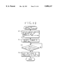
- FIG. 1 is a block diagram of a conventional multiprocessor system
- FIG. 2 is a block diagram of a multiprocessor module construction of the present invention
- FIG. 3 is a block diagram of an internal construction of the processor module of FIG. 2;
- FIG. 4 is a block diagram of an internal construction of the processor module of FIG. 3;
- FIG. 5 is an explanatory diagram of a cache line of the present invention.
- FIG. 6 is a functional explanatory diagram of a space identification unit in FIG. 3;
- FIG. 7 is a block diagram of a memory management unit in FIG. 4.
- FIG. 8 is an explanatory diagram of a directory entry register of the present invention.
- FIG. 9 is an explanatory diagram of a shared map 37 bit correspondence register
- FIG. 10 is an explanatory diagram of a processor module construction register of the present invention.
- FIG. 11 is an explanatory diagram of the directory entry register, shared map bit correspondence register, and processor module construction register of the present invention.
- FIG. 12 is an explanatory diagram of the directory entry register of the present invention.
- FIG. 13 is a command explanatory diagram for a snoop bus in FIG. 4;
- FIG. 14 is an explanatory diagram of a cache state of a cache unit in FIG. 4;
- FIG. 15 is an explanatory diagram of a cache transition state of the cache unit in FIG. 4;
- FIG. 16 is an explanatory diagram of the processing operation in a reading mode 1 of the present invention.
- FIG. 17 is an explanatory diagram of the processing operation in a reading mode 2 of the present invention.
- FIGS. 18A and 18B are explanatory diagrams of the processing operation in a reading mode 3 of the present invention.
- FIG. 19 is a flowchart for a reading process of a local processor module of the present invention.
- FIG. 20 is a flowchart for a reading process of a home processor module of the present invention.
- FIG. 21 is a flowchart for a reading process of a remote processor module of the present invention.
- FIG. 22 is a flowchart for a reading process of a processor element of the present invention.
- FIG. 23 is an explanatory diagram of the processing operation in a writing mode 1 of the present invention.
- FIG. 24 is an explanatory diagram of the processing operation in a writing mode 2 of the present invention.
- FIG. 25 is an explanatory diagram of the processing operation in a writing mode 3 of the present invention.
- FIG. 26 is an explanatory diagram of the processing operation in a writing mode 4 of the present invention.
- FIG. 27 is an explanatory diagram of the processing operation in a writing mode 5 of the present invention.
- FIG. 28 is an explanatory diagram of the processing operation in a writing mode 6 of the present invention.
- FIG. 29 is an explanatory diagram of the present processing operation in a writing mode 7 of the invention.
- FIG. 30 is a flowchart for a writing process of the local processor module of the present invention.
- FIG. 31 is a flowchart for a writing process of the home processor module of the present invention.
- FIG. 32 is a flowchart for a writing process of the remote processor module of the present invention.
- FIG. 33 is a flowchart for a writing process of the processor element of the present invention.
- FIG. 34 is an explanatory diagram of the operation in which an internal command and an external remote command to a cache unit compete and a retry is repeated of the present invention
- FIG. 35 is a time chart of a specific example of a retry repetition of FIG. 34;
- FIG. 36 is a time chart for processes of the present invention in the case where a retry instruction to a remote command is set once and is preferentially accepted;
- FIG. 37 is an explanatory diagram for a movement of a write privilege (owner) which is executed between the cache units of the processor module of the present invention
- FIG. 38 is an explanatory diagram of the order for transmitting the write privilege of the present invention.
- FIG. 39 is an explanatory diagram of a system construction extended on the basis of the cache coherence apparatus of FIG. 3;
- FIG. 40 is an explanatory diagram of a line construction of a system bus in FIG. 39;
- FIG. 41 is an explanatory diagram of a tag bus code by a tag bus line in FIG. 40;
- FIG. 42 is an explanatory diagram of control contents according to a combination of a request line and an emergency request line in FIG. 40;
- FIG. 43 is an explanatory diagram of control contents according to a combination of a halt line and a master right change-over line in FIG. 40;
- FIG. 44 is a time chart for a bus arbitration in a fast mode of the system bus in FIG. 40;
- FIG. 45 is a time chart for a bus arbitration in a safety mode of the system bus in FIG. 40;
- FIG. 46 is a time chart for a preferential bus arbitration when an error is detected in a bus slave of the system bus in FIG. 40;
- FIG. 47 is a time chart for the preferential bus arbitration when an error is detected in a bus arbiter of the system bus in FIG. 40;
- FIG. 48 is a time chart for a transfer sequence of a memory read of the system bus in FIG. 39;
- FIG. 49 is a time chart for a transfer sequence of a memory write of the system bus in FIG. 39;
- FIG. 50 is a time chart for a transfer sequence of broadcast/broadcall of the system bus in FIG. 39;
- FIG. 51 is a time chart for a transfer sequence between system buses in FIG. 39;
- FIG. 52 is a time chart for a transfer sequence between subsystem buses in FIG. 39;
- FIG. 53 is a time chart for a transfer sequence in the case where the system bus in FIG. 39 is an 8-byte bus;
- FIG. 54 is a time chart for a transfer sequence between the system bus and a heterosystem bus in FIG. 39;
- FIG. 55 is an explanatory diagram for a format of a fundamental bus command of the system bus in FIG. 39;
- FIG. 56 is an explanatory diagram for a format of a broadcast bus command of the system bus in FIG. 39;
- FIG. 57 is an explanatory diagram for a format of a fundamental reply/error bus command of the system bus in FIG. 39;
- FIG. 58 is an explanatory diagram for a format of a cache status bus command of the system bus in FIG. 39;
- FIG. 59 is an explanatory diagram of an error type which is designated by the error bus command in FIG. 57;
- FIG. 60 is an explanatory diagram of an error level and an error type which are designated by the error bus command in FIG. 57;
- FIG. 61 is an explanatory diagram of a cache status which is designated by the cache status bus command in FIG. 58;
- FIG. 62 is an explanatory diagram for a format of an extension bus command which is added to a fundamental bus command and used upon bus transfer between the subsystem buses in FIG. 39;
- FIG. 63 is an explanatory diagram for a write access of an embodiment in which a second directory memory is provided for the bus connection unit of the present invention.
- FIG. 64 is an explanatory diagram for an access in the case where an access request to a home becomes buffer full due to the waiting for the completion of a cache invalidation in FIG. 63.
- FIG. 2 is a block diagram of a multiprocessor system to which a cache coherence apparatus of the present invention is applied.
- the system has, for example, five processor modules 10-1 to 10-5 as processor groups each having at least one processor element.
- the processor modules 10-1 to 10-5 are mutually connected through system buses 12-1 and 12-2 as external common buses.
- each of the processor modules 10-1 to 10-5 has, for example, four processor elements 14-1 to 14-4 which are mutually connected through a snoop bus 22 as an internal common bus.
- the processor elements 14-1 to 14-4 comprise processors 16-1 to 16-4, cache units 18-1 to 18-4, and snoop units 20-1 to 20 respectively.
- a memory control module 25 is connected to the snoop bus 22 and is also connected to the system buses 12-1 and 12-2 by another port.
- the memory control unit 25 recognizes the processor module in which the access data exists including itself.
- an access command is transmitted by the system bus 12-1. This means that there is a case where an access command is received from another processor module by the system bus 12-1.
- the memory control module 25 refers to a directory memory 30 and accesses a local storage 28 as its distributed main storage and responds to a transmitting source if the access data is not registered yet.
- the memory control module 25 accesses the cache unit of the registration destination and responds.
- a cache unit to be accessed in this case there is a case where it is any one of the cache units 18-1 to 18-4 in the processor module or there is also a case where it is a cache unit of another processor module.
- the memory control module 25 updates a state of the directory memory 30 in accordance with the access result.
- the memory control module 25 has a protocol management unit 24, a memory management unit 26, and a bus connection unit 32.
- the protocol management unit 24 executes a protocol conversion between the system buses 12-1 and 12-2 and the internal snoop bus 22
- the bus connection unit 32 executes a bus access between the memory control module 25 and the system buses 12-1 and 12-2.
- the local storage 28 which functions as a distributed main storage and the directory memory 30 which is used to maintain a cache coherence between the processor modules are connected to the memory management unit 26.
- the snoop units 22-1 to 22-4 maintain the cache coherence between the local storage 28 and the cache units 18-1 to 18-4 in accordance with a snoop protocol for snooping a plurality of cache units 18-1 to 18-4 synchronized with a specific machine cycle by the snoop bus 22
- a cache coherence with another processor module is performed by a cache conversion unit 80 provided in the memory management unit 26.
- the cache conversion unit 80 maintaining the cache coherence between the processor modules on the basis of the reference to the directory memory 30 through the transmission and reception with the other processor modules using the system buses 12-1 and 12-2.
- the processor element 14-1 is shown in FIG. 4 as a representative.
- a CPU 34 having a primary cache 36 is provided for the processor 16-1.
- a secondary cache 38 is connected to the outside of the CPU 34.
- a secondary cache control module 35 is provided as a controller of the secondary cache 38.
- a tag memory 40 is connected to the secondary cache control module 35.
- the primary cache 36 of the CPU 34 is controlled by a write through.
- the secondary cache 38 is controlled by a copy back.
- an address of data in the secondary cache 38 and information indicative of a cache state of its entry have been registered in the tag memory 40.
- cache data has been registered in the secondary cache 38 as data of a 256-byte unit.
- the cache control module 35 manages the cache registration on an address unit basis of 256 bytes.
- the data of a 256-byte unit on the secondary cache 38 is called a cache line 100. Therefore, an address of the cache line 100 of the 256-byte unit is held in the tag memory 40.
- the cache line 100 of 256 bytes is divided into sublines 102-1 to 102-4 of a 64-byte unit. A cache state is held for every sublines 102-1 to 102-4
- the secondary cache 38 is controlled so as to always include the primary cache 36 of the CPU 34. To guarantee a coherence of data among the cache units 18-1 to 18-4 of, for example, the four processor elements 14-1 to 14-4 in FIG.
- the secondary cache 38 is snooped by the snoop bus 22
- the snoop bus 22 is a bus by a packet protocol and has a snoop transmission and reception unit 42, a snoop buffer 44, a copy back buffer 46, and a processor access unit 48 as a snoop mechanism of the secondary cache 38.
- various kinds of snoop commands are prepared for the snoop bus 22 Since the snoop bus is based on the packet protocol, a plurality of accesses can be simultaneously processed.
- the snoop of the secondary cache 38 is simultaneously executed by the secondary cache control module 35 of the processor elements 14-1 to 14-4 connected to the snoop bus 22
- the results are simultaneously reflected to a cache state signal that is unique to the processor element on the snoop bus 22
- the cache state signal is referred by all of the processor elements 14-1 to 14-4 and the memory control module 25 which are connected to the snoop bus.
- a space identification unit 50, a snoop transmission and reception unit 52, and a snoop bus transmission unit 60 are provided.
- the secondary cache control module 35 of the processor element 14-1 displays the cache state by the cache state signal.
- the memory management unit 26 provided for the memory control module 25 also has a memory state signal to display a state of the local storage 28 in which the main storage is divisionally arranged.
- the memory state signal is also supplied to all of the secondary cache control modules 35 in the snoop bus 22
- Each of the secondary cache control modules 35 provided for the processor elements 14-1 to 14-4 judges the processor element which responds to the access of the CPU 34, determines what an owner having the newest value of the cache data as a target of the access in a possessing state of the write privilege, and judges whether various snoop commands are proper or not on the basis of the contents of the cache state signal regarding the secondary cache 38 on the snoop bus 22 and the memory state signal of the local storage 28 connected to the memory control module 25.
- the cache state of the secondary cache 38 held in the tag memory 40 is changed as necessary. Further, there is also a case where the invalidation of the primary cache 36 or the response of the data from the secondary cache 38 is associated. Such a series of operations by the snoop bus 22 are controlled in a pipeline manner.
- the busy display is performed when the reception command cannot be processed because of a lack of processing resources or at a timing when a contradiction on the protocol occurs.
- the "mis”, “clean”, and “dirty” displays correspond to the snoop result of the tag memory 40 of the secondary cache 38. Namely, as a result of the secondary cache 38 being snooped by the address of the snoop command, when a mishit in which the data in the address is not held in the secondary cache 38 is detected, the "mis" display is performed.
- the "clean" display is executed.
- the "dirty" display is executed. Since there is a responsibility to respond by writing into the local storage 28, such a state is referred to as an owner who possesses the write privilege.
- the cache coherence is held among the processor elements 14-1 to 14-4 by the snoop system using the snoop bus 22
- the memory management unit 26 is provided for the memory control module 25.
- the local storage 28 is connected to the memory management unit 26 through memory buses 66.
- the directory memory 30 is also connected to the memory management unit 26 through an exclusive-use line.
- memory access units 68-1 to 68-4 and SRAMs 70-1 to 70-4 as main storage elements are connected for every four memory buses 66.
- Each of the memory buses 66 has a width of 32 bits. By simultaneously accessing two memory buses, data of one word which coincides with the width of 64 bits of the subline in the cache line is accessed.
- the local storage 28 is divided into four groups by the four memory buses 66.
- the access can be executed by an interleave system such that the access of one word is performed by two groups of the memory access units 68-1 and 68-2 and the access of one word is performed by the memory access units 68-3 and 68-4.
- the memory control module 25 enables the space identification unit 50 to map the memory space in the local storage 28 connected by the memory management unit 26 into a physical space that can be referenced from all of the processor modules 10-1 to 10-5.
- FIG. 6 shows a mapping function of the space identification unit 50 in FIG. 4.
- a CPU physical address space 86 of the CPU 34 provided for the processor element 14-1 has an address space of, for example, 64 GB (gigabytes). Among them, the area of 0 to 4 GB at the head is allocated to a control register space 88 that is used by the CPU. The last area of 60 to 64 GB is allocated to a ROM space 92 of the CPU. The area of a width of 56 GB of the remaining 4 to 60 GB is set as shared space 90 which can be accessed by all of the CPUs 34 provided for processor modules 10-1 to 10-5.
- the 36-bit physical address 94 is transmitted to the space identification unit 50 of the memory control module 25 via the snoop bus 22 by a snoop command.
- the physical address 94 is transmitted to space identification unit 50 through the snoop bus 22 in the case where a cache line of physical address 94 as an access target doesn't exist on the caches of the processor elements 14-1 to 14-4 connected by the snoop bus 22
- the space identification unit 50 holds a control table 95. Entries of addresses of 4 to 60 GB of the shared space 90 are provided in the control table 95. An ID area is provided in correspondence to the entry by the address.
- a unit ID is registered in the corresponding ID area as information indicative of the processor module to which the address in the shared space 90 is allocated.
- the unit ID physically shows a slot number at which the processor module can be connected to the system buses 12-1 and 12-2 in FIG. 2.
- the unit IDs #00 to #07 are registered in correspondence to the addresses of 4 to 24 GB.
- Home information 96, a unit ID 98, and the 36-bit physical address 94 are formed as formation information by the access to the space identification unit 50 by the 36-bit physical address 94 from the snoop bus 22
- the home information 96 indicates whether the accessed physical address 94 corresponds to the home or not, namely, whether the physical address 94 exists in the processor module itself which caused the access or not.
- the unit ID 98 indicates the processor module in which the physical address 94 exists.
- the memory control module 25 is accessed from the CPU 34 of the processor element 14-1 through the snoop bus 22 and is also accessed from the CPUs 34 provided for the other processor modules 10-2 to 10-5 through the system bus 12-1 (including 12-2).
- the cache coherence between the caches provided in the processor module 10-1 is maintained by using the snoop bus 22, the cache coherence is held among the processor modules 10-1 to 10-5 by a directory method using the system buses 12-1 and 12-2.
- the entries have been stored in the directory memory 32 on a cache line unit basis of 256 bytes. The directory entry is selected by the 36-bit physical address generated by the CPU access and displays the state of the cache line.
- the identification (ID) information of the processor module having the rewritten newest data is held in the memory management unit 26. Also in the case where the cache line is share, the ID information of the processor module having the copy of the data of the local storage 28 is held in the memory management unit 26.
- FIG. 7 shows the details of the memory management unit 26 provided for the memory control module 25 in FIG. 4.
- a bus arbiter 74, a memory bus control unit 76 to which the local storage 28 is connected through the memory buses 66, and a directory control unit 78 to which the directory memory 30 is connected by an exclusive-use line are provided for the memory management unit 26.
- the cache conversion unit 80 is provided for the memory management unit 26.
- the cache conversion unit 80 has a local state machine 81, a home state machine 82, and a remote state machine 83.
- the processor module which activated the access is called a local and the processor module in which the accessed address is possessed in the local storage is called a home.
- the processor module in which the address of the accessed local storage is in a "dirty" state, namely, only the old data exists in the address of the local storage, and to which the processor element in which the newest data is possessed in the caches of the other processor modules belongs is called a remote.
- the local state, home state, and remote state of the processor module are maintained by processing operations of the local state machine 81, home state machine 82, and remote state machine 83 provided for the cache conversion unit 80, respectively.
- a local access buffer queue 54 is provided in correspondence to the local state machine 81.
- Home information Home as a formation information in FIG. 6 formed by the space identification unit 50, the unit ID, and the 36-bit physical address are stored into the local access buffer queue 54.
- a response interruption INT is given to the local access buffer queue 54 from the snoop transmission and reception unit 52.
- information is a variable called full indicative of the full state is returned to the snoop transmission and reception unit 52.
- a home access buffer queue 56 is provided for the memory control module 25.
- An access command from the processor module as a local which was generated by using the system buses 12-1 and 12-2, namely, what is called a home command is stored in the home access buffer queue 56.
- a remote access buffer queue 58 is provided in correspondence to the remote state machine 83.
- An access command generated from the processor module as a home by using the system buses 12-1 and 12-2, namely, what is called a remote command is stored in the remote access buffer queue 58.
- the access of the local storage 28 is associated with each of the local state machine 81 and home state machine 82 provided for the memory management unit 26.
- the remote command of the remote access buffer queue 58 relates to the access for the cache line on the secondary cache 38 of the processor element 14-1 as a target, it is directly connected to the snoop bus 22 by the snoop bus transmission unit 60.
- FIG. 8 shows a directory entry register 104 provided for the directory control unit 78 provided for the memory management unit 26.
- the contents of the directory entry register 104 show the read result of the directory entry for every cache line stored in the directory memory 30. Therefore, the contents of the directory entry register 104 are nothing but the read result, namely, the directory entry data itself stored in the directory memory 30.
- the directory entry register 104 allocates a shared map bit area 106 to lower eight bits.
- the shared map bit area 106 relates to bits indicating that the data exists on the secondary cache of which processor module by referring to the data corresponding to the cache line of the local storage 28 as a distributed main storage in the processor module.
- Reference numeral 110 denotes a busy bit and 111 indicates a parity bit.
- a shared map bit correspondence register 112 in FIG. 9 is combined to the shared map bit area 106. Further, a processor module construction register 114 in FIG. 10 is combined to the shared map bit correspondence register 112 in FIG. 9.
- the shared map bit area 106 of the directory entry register 104 has bits S0 to S7. By setting the bits S0 to S7 to 1, it indicates that the data of the cache line exists as a share state on the processor module shown by the shared map bit correspondence register 112.
- the shared map bits S0 to S7 have eight bits of S0 to S7, whose number is only the half of the number of 16 bits. Therefore, by overlappingly storing the shared map bits in the shared map bit area 106 into the shared map bit correspondence register 112, the shared map bits can be expressed with respect to a plurality of processor modules, thereby realizing a reduction of the number of bits of the directory entry register 104. Further, the shared map bits S0 to S7 to be stored in the shared map bit area 106 are held for every cache subline of 64 bytes which are obtained by dividing the cache line of 256 bytes into four sublines on the secondary cache. On the other hand, since the shared map bit is only one bit, the share states of the four cache sublines are expressed by the OR.
- the processor element in which the cache line in the share state exists can be accessed without being aware of it.
- the OR expression of a plurality of sublines can be performed.
- Processor module installation bit area 116 and a bus ID bit area 118 are provided for the processor module construction register 114 in FIG. 10 provided in correspondence to the shared map bit correspondence register 112 in FIG. 9. Bus IDs divided into the system buses 12-1 and 12-2 are stored in the bus ID bit area 118. Each of the system buses 12-1 and 12-2 has sixteen slots. Therefore, up to sixteen processor modules can be installed.
- the processor module installation bit area 116 has bit areas corresponding to the same slot numbers #00 to #15 as those of the unit IDs in a one-to-one corresponding relation. Bit 1 is set in the installation state and is reset to bit 0 in the uninstallation state.
- FIG. 11 shows the specific correspondence relations among the directory entry register 104, shared map bit correspondence register 112, and processor module construction register 114.
- the processor module construction register 114 only the processor module installation bit area 116 is shown and the processor module in which the unit ID set to bit 1 is installed is shown.
- the bits of the processor module construction register 114 correspond to the bits of the shared map bit correspondence register 112 in a one-to-one relation.
- a "dirty" subline bit area 108 is provided.
- bits D0 to D3 are allocated to the "dirty" subline bit area 108.
- the "dirty" subline bits D0 to D3 By setting the "dirty" subline bits D0 to D3 to bit 1, it is shown that the rewritten newest data exists on the cache of any one of the processor modules in the system for the old data of the local storage 28 as a distributed main storage.
- the "dirty" subline bit area 108 is reset to bit 0, this means a "non-dirty" state.
- non-dirty state it means that the newest data exists in the local storage 28 as a distributed main storage and the copy data exists as a share state on the cache of any one of the processor modules that is designated by the shared map bits S0 to S7.
- the identification information of the processor modules regarding the data subline bits D0 to D3 is stored in a specific area on the local storage 28 as a main storage, for example, in the control register space 88 in the CPU physical address space 86 in FIG. 6.
- FIG. 12 shows the specific contents of the directory entry register 104.
- the shared map bit area is divided into shared map bit areas 106-1 and 106-2 in correspondence to the system buses 12-1 and 12-2.
- the shared map bit area 106-1 side is used for the installed processor modules.
- bit 1 is set in the shared map bits S3 and S4.
- the "dirty" subline bit area 108 for example, the "dirty" subline bits DI and D4 are set to bit 1 and the bits D2 and D3 are reset to bit 0.
- processor module information storage areas 120, 122, 124, and 126 are provided for the local storage 28.
- the "dirty" subline bit D4 which was set to bit 1
- the processor module information storage areas 122 and 124 of the "dirty" subline bits D2 and D3 which were reset to bit 0 it is shown that the newest data exists in the local storage as a distributed main storage in which the physical address of the cache line exists and that the copy data by the reference of the newest data of the main storage exists as a share state on the cache of any one of the processor modules.
- the packet is classified into an activation command and a response command.
- the activation command and the response command are fundamentally constructed as a pair.
- the packet comprises a command phase and a data phase.
- the command phase has a length of one clock.
- the data phase can have a length within a range from 0 to 8 clocks in accordance with a command and a size.
- the command phase of the activation command is constructed by: a destination field indicative of a destination of the packet; a flag field including an auxiliary instruction with respect to a packet process; a size field indicative of a data size as a processing target; a type field indicative of the type of command; and an address field indicative of an address as a processing target of the command.
- the activation command and the response command are distinguished by the type field.
- the response command is also constructed by a command phase and a data phase.
- the command phase can have a length of one clock.
- the data phase can have a length within a range from 0 to 8 clocks depending on the command and size.
- the command phase of the response command is constructed by: a destination field indicative of a destination of the packet; a reply code field indicative of a permission or inhibition of the access, and error factors and a retry instruction; a reply field indicative of the type of reply; a command field (kind information indicative of the reply is stored) indicative of the kind of command; and an address field indicative of an address of a processing target of the command.
- the packet is fundamentally the same as that of the snoop bus 22 but the bus clock differs. Namely, since the snoop bus is short because a line length of the bus lies within a module casing and electric characteristics are good, for example, a clock frequency can be set to 60 MHz. On the other hand, in case of the system buses 12-1 and 12-2, since a line length is long because they are connected among a plurality of processor modules through a back panel and a clock frequency is limited to, for example, 40 MHz from the limitation of the electric characteristics.
- FIG. 13 separately shows the kinds of commands which are used by the snoop bus 22 with regard to the processor 16, snoop unit 20, and memory management unit 26.
- the cache states are held in the tag memory 40 of the secondary cache control module 35 on a cache subline unit basis.
- There are five kinds of cache states such as “invalid”, “shared & clean”, “shared & modified”, “exclusive & dirty”, and “shared & dirty” as shown in FIG. 14.
- the "invalid” state is a non-cache state in which no data exists on the secondary cache 38.
- the "shared & clean” state indicates the data of the same contents as those of the local storage as a distributed main storage of the processor module serving as a home is held.
- the "shared & modified" state indicates although the data on the main storage serving as a home is not the newest data, it is the old data and its copy data exists in the secondary cache itself and, further, the newest data that is unique in the system exists on another secondary cache its processor module by "exclusive & dirty".
- the "exclusive & dirty" state indicates the newest data that is unique in the system is reserved. In this case, the cache control module is what is called an owner who possesses the write privilege.
- shared & dirty is a state in which no newest data exists on the main storage serving as a home, the newest data is reserved in the secondary cache group in its processor module, further, “shared & modified” having the copy of the data in the main storage as a home exists in the secondary cache group in the processor module, and the cache control module which reserves the newest data possesses the write privilege and becomes an owner.
- FIG. 15 shows a transition of the cache state in the secondary cache control module 35 in FIG. 4.
- the initial state is the invalidation of block 130.
- an access request is generated to the secondary cache control module 35.
- the relevant cache subline of the secondary cache 38 is "invalid”
- a command to request the data is transmitted to the snoop bus 22
- transition states there are two cases such as case 1 of shifting to "shared & modified" of a block 150 and case 2 of shifting to "shared & clean" of a block 140.
- "shared & modified" of the block 150 relates to the case where the other processor elements are in the "exclusive & dirty” state or “shared & dirty” state and the subline as an accessing target is possessed on the cache.
- the "dirty” is displayed by a cache state signal of any one of the processor elements. Therefore, the cache control module 35 of the processor element in which "dirty” is displayed accesses the secondary cache 38 and generates a data response to the snoop bus 22 In this instance, in the processor element which made a response, when the cache state is "exclusive & dirty" of a block 160, the state is shifted to "shared & dirty" of a block 170.
- the processor element which received the response shifts the cache state to "shared & modified, of the block 150.
- the other processor elements are "shared & clean” of the block 140 or "invalid” of the block 130, so that "clean” or “mis” is displayed as a cache state signal and a memory state signal on the memory control module 25 side.
- the cache control module 35 which displayed "clean” refers to the cache state signal and judges whether a response should be formed or not.
- the memory control module 25 which referred to the memory state signal namely, the memory management unit 26 provided for the memory control module 25 also refers to the memory state signal and judges whether a response should be formed.
- the secondary cache control module 35 When the module which detected that the response should be made is the secondary cache control module 35, it accesses to the secondary cache memory 38 and generates the transmission of the data to the snoop bus 22 When the module which detected that the response should be made is the memory management unit 26 of the memory control module 25, it activates the access to the local storage 28 serving as a main storage and generates response data to the snoop bus 22
- the secondary cache control module 35 of the accessing source which received the response data from the snoop bus 22 is shifted from "invalid" of the block 130 to "shared & clean" of the block 140.
- FIG. 16 shows a protocol of the cache coherence in the reading mode 1.
- the reading mode 1 relates to the case where for a read access P-RD of an arbitrary CPU in the processor module 10-1, a mishit occurs in the cache unit in a cache unit group 18 and a mishit occurs in all of the other cache units 18 connected by the snoop bus 22 In this case, since the local storage 28 as a distributed main storage is accessed to the memory management unit 26, a remote command T-CR is generated.
- the processor module 10-1 Since the read address exists in the local storage 28 of the processor module 10-1, it is assumed that the processor module 10-1 becomes a home and, further, the data of the local storage 28 exists as a "dirty" state in which the newest data is possessed in any one of the group of cache units in the processor module 10-2 serving as a remote. In such a case, the memory management unit 26 of the processor module 10-1 which generated the read access generates a remote command 220 to a system bus 12 and accesses to the processor module 10-2.
- the memory management unit 26 of the processor module 10-2 which received the remote command 220 obtains the newest data from the cache unit in the "dirty" state D through the snoop bus 22 After that, the memory management unit 26 transmits the newest data as reply data 230 by using the system bus 12 to the processor module 10-1 which is local and a home.
- the processor module 10-1 stores the reply data 230 derived as a response of the system bus 12 into the cache unit of the accessing source through the snoop bus 22, thereby responding as read data for the read access of the CPU.
- the cache coherence is maintained.
- the cache unit of the processor module 10-2 which responded by receiving the remote command 220 updates "dirty” to "clean".
- "dirty D" of the cache line as an accessing target is updated to "share S”.
- "invalid I” is updated to "clean C”.
- FIG. 17 shows a protocol for the cache coherence in the reading mode 2.
- the reading mode 2 relates to the case where for the read access P-RD of an arbitrary CPU, a mishit occurs in its cache unit, a mishit occurs in all of the other cache units connected by the snoop bus 22, and further, the read address exists in the local storage 28 of the other processor module 10-2, and the data in the read address of the local storage 28 exists in "dirty D" state in which the newest data is possessed on any one of the cache units of the other processor module 10-3.
- the memory management unit 26 of the processor module 10-2 in which the read access occurred operates as a local, generates a home command 240 to the system bus 12, and accesses to the processor module 10-2.
- the processor module 10-2 On the basis of the home command 240 received from the system bus 12, the processor module 10-2 recognizes that the newest data exists as "dirty D" on the cache of the processor module 10-3 by referring to the directory memory by the read address, generates a remote command 250 to the system bus 12, and accesses to the processor module 10-3.
- the memory management unit 26 On the basis of the remote command 250 received from the system bus 12, the memory management unit 26 operates as a remote and the processor module 10-3 accesses to the cache unit in "dirty D" by the snoop bus 22, thereby obtaining the newest data.
- the processor module 10-3 responds reply data 260 to each of the processor module 10-2 as a home and the processor module 10-1 as a local by using the system bus 12.
- the processor module 10-2 as a home writes the corresponding data of the local storage 28 by the reply data 260 derived by the response of the system bus 12 and updates to the newest data.
- the processor module 10-1 as a local transfers the reply data 260 received by the response from the system bus 12 to the cache unit of the accessing source through the snoop bus 22 and stores onto the secondary cache, thereby responding as read data for the read access of the CPU.
- the cache unit which transmitted the newest data by the processor module 10-3 as a remote updates the cache state from "dirty D" to "clean C”.
- the processor module 10-2 as a home updates the state of the cache line as an accessing target from "dirty D" to "share S".
- the corresponding subline bits in the "dirty" subline bit area 108 of the directory entry register 104 in FIG. 8 are reset from 1 to 0. Since the processor module 10-3 as a remote and the processor module 10-1 as a local have share, in which the same data as the data of the local storage 28 as a home exists, the corresponding shared map bits in the shared map bit area 106 are set to 1. Further, in the cache unit in which the access of the processor module 10-1 as a local occurred, the "invalid" state I is shifted to the "clean" state C.
- FIGS. 18A and 18B show a protocol of the cache coherence in the reading mode 3.
- the reading mode 3 the cache coherence using the snoop bus 22 among the cache units in the module in which the access occurred is executed.
- the reading mode there are two cases of FIGS. 18A and 18B.
- FIG. 18A shows the case where although the cache unit 18-4 in which the read access P-RD of the CPU occurred is invalid, and a mishit occurred, the newest data exists as shared & clean, in the other cache unit 18-1 connected by the snoop bus 22
- the cache unit 18-4 generates the command T-CR by using the snoop bus 22
- reply data 270 including the relevant subline is received from the cache unit 18-1, and the reply data 270 is stored onto the cache unit 18-4 and transmitted as read data for the read access.
- the cache unit 18-4 of the accessing & clean SH&C In the cache unit 18-1 of the accessing destination, the "shared & clean" state is maintained.
- FIG. 18B relates to the case where for the read access P-RD from the CPU to the cache unit 18-4 in the "invalid" state, the newest data exists as "exclusive & dirty" in the cache unit 18-1 connected by the snoop bus 22, namely, the case where the newest data exists in a state in which the write privilege is possessed.
- the reply data 280 including the subline of the newest data is similarly responded from the cache unit 18-1.
- the cache unit 18-4 of the accessing source is shifted from "invalid” to "shared & modified", namely, indicates that the newest data exists as "shared & dirty" in the other cache unit in the processor module.
- the cache unit 18-1 of the accessing destination it is shifted from "exclusive & dirty" to "shared & dirty".
- a flowchart of FIG. 19 shows the reading processes of the processor module serving as a local in the reading modes 1 and 2 in FIGS. 16 and 17.
- step S1 the read access of the processor element is received.
- step S2 the presence or absence of the cache hit is judged.
- step S14 the data is transmitted to the processor element and the processing routine is finished.
- step S3 a cache status is obtained from the tag memory 40 in step S3.
- step S4 A check is made in step S4 to see if the newest data exists on the cache of another processor element. If the newest data exists on the cache of another processor element, step S15 follows and a command is transmitted to the snoop bus 22.
- step S16 the reply data is received.
- step S13 the reply data is stored into the cache and is responded to the processor element.
- Steps S15 to S17 relate to the processes in the reading mode 3 in FIG. 18.
- a local command is transmitted to the memory management unit 26 through the snoop bus 22 in step S5.
- step S6 a processor module space is determined from a physical address of the command by the space identification unit 50 in FIG. 4.
- step S7 when the read address exists in the main storage space of the local storage 28 of the processor module, the self processor module is set to a home and the cache status is obtained from the directory entry in the directory memory 30 in step S8.
- step S9 a check is made in step S9 to see if the subline is "dirty". If it is dirty, a remote command is transmitted to the remote processor module through the system bus in step S10. When there is a response in step S11 for the remote command, the reply data is written into the local storage 28 as a distributed main storage in step S12 and the state is updated from "dirty" to "shared". In step S13, a response is made to the cache unit of the accessing source and the processing routine is finished.
- step S9 When the subline is not "dirty" in step S9, the data is read out from the local storage 28 as a main storage and is transmitted to the cache unit of the accessing source in step S22 In step S23, the shared bit of the subline of the local storage 28 as a main storage is turned on.
- step S7 when the accessed physical address exists in the other processor module space, a home command is transmitted to the processor module serving as a home through the system bus in step S18.
- step S19 In response to the transmission of the home command, since there is a reply of the newest data through the system bus, when the reply is determined in step S19, a response is made to the cache every access in step S20 and the processing routine is finished.
- a flowchart of FIG. 20 relates to the reading processes of the processor module serving as a home in the reading modes 1 and 2 in FIGS. 16 and 17.
- the home command is received.
- a home command there are a case where it is received via the system bus and a case where when the processor module itself is local and is a home, the home command formed by itself is received.
- the processor module itself is set to a home and the status of the cache line is obtained from the directory memory 30 in step S2.
- a check is made in step S3 to see if the subline is "dirty".
- a check is made in step S4 to see if the newest data exists in the cache of the processor element in the its processor module.
- step S5 a command is transmitted to the snoop bus 22 in step S5.
- the processor module waits for the reply in step S6.
- step S7 the reply data is written into the local storage 28 as a distributed main storage and "dirty" of the directory entry is updated to "shared".
- step S8 the reply data is transmitted to the local processor module by using the system bus.
- step S4 when the newest data of a "dirty" state exists on the cache of the processor element in the other processor module, a remote command is transmitted to the remote processor module through the system bus in step S12.
- the processor module waits for the reply in step S13.
- step S14 the newest data is written into the local storage 28 and the "dirty" state of the directory entry is updated to the "shared" state.
- the subline is not "dirty” in step S3
- the newest data is read out from the local storage 28 and the reply data is transmitted to the local processor module through the system bus.
- the processing routine is finished.
- a flowchart of FIG. 21 relates to the reading processes of the remote processor module in the reading modes 1 and 2 in FIGS. 16 and 17.
- step S1 when the remote command is received through the system bus, the processor module itself is set to a remote and transmits the remote command to the cache unit through the snoop bus in step S2.
- step S2 When the reply of the data is received from the cache unit of the relevant processor element, the reply data is received from the snoop bus 22 in step S4.
- step S5 the reply data is transmitted to the home processor module and local processor module through the system bus.
- step S1 when a read request is generated from the CPU, the presence or absence of the cache hit is judged in step S2. If there is a cache hit, the cache data is transmitted for the read access in step S12. When a cache mishit occurs, the status of the cache line is derived from the tag memory 40 by the cache control module 35 in step S3. A check is made in step S4 to see if the hit has occurred on the cache of the other processor element. In this case, when there is a mishit, step S13 follows and the processes for the other processor module are executed by the access to the memory control module 25 side.
- step S5 When there is a cache hit in step S4, a check is made in step S5 to see if the cache state of the other processor element is "shared & clean" or not. If this is the case, a command is transmitted to the snoop bus 22 in step S6. The reply data is received and responded to the cache in step S7. The status is updated from "invalid" to "shared & clean” in step S8. On the other hand, when the other processor is "exclusive & dirty", the command is transmitted to the snoop bus 22 in step S9. After that, the reply data is received and responded to the cache in step S10. In step S11, the status is updated to "shared & modified".
- FIG. 23 shows a protocol of the cache coherence in the writing mode 1.
- the writing mode 1 relates to the case where a mishit occurs in the cache unit for a write access P-WT of an arbitrary CPU of the processor module 10-1, a mishit also occurs in the other cache units connected by the snoop bus 22, the write address exists in the local storage 28 as a distributed main storage of the processor module 10-1, and further, the copy data in the write address of the local storage 28 exists as a "share" state on the caches of the other plurality of processor modules 10-2 and 10-3.
- the memory management unit 26 of the processor module 10-1 which received a write access T-CRI through the snoop bus 22 sets itself to a local and a home and generates a purge command 300 as an invalidating command to all of the processor modules 10-2 and 10-3 which are in the "share” state by using the system bus 12 with reference to the cache directory.
- the processor modules 10-2 and 10-3 operate as a remote and each memory management unit 26 requests the invalidation to the memory units in "share C" through the snoop bus 22
- the processor modules 10-2 and 10-3 independently make purge responses 310 and 320 by using the system bus 12.
- the cache statuses of the cache lines which became the targets in the processor modules 10-2 and 10-3 are included in the purge responses 310 and 320.
- the processor module 10-1 of the home recognizes the success in invalidation because it received all of the purge responses 310 and 320 from the system bus 12, stores the copy data in the write address of the local storage 28 into the cache unit of the accessing source, and overwrites the copy data by the write access.
- the processor module 10-1 as a home updates "share S" of the directory entry of the cache line as an accessing target to "dirty D".
- the same data as that of the local storage 28 is changed by the overwriting and becomes the newest data on the cache of the accessing source, so that the processes are finished while the data in the local storage 28 is held as old data and the coherence between the old data and the newest data in the local storage 28 is executed through the read access, which has previously been described.
- FIG. 24 shows a protocol of the cache coherence in writing mode 2.
- Writing mode 2 relates to the case where the same data as that of the local storage 28 exists in the cache unit of the processor module 10-1 in which the CPU access occurred, and in this case, the data exists in the "share C" state in which the write privilege is not possessed in the other cache units connected by the snoop bus 22 The other states are the same as those in the writing mode 1 in FIG. 23.
- the purge command 300 is generated from the memory management unit 26 which operated as a home to the processor modules 10-2 and 10-3 serving as a remote by using the system bus 12.
- a purge command 325 is generated to the cache unit group 18 in the same processor module 10. Therefore, the memory management unit 26 of the processor module 10-1 as a home recognizes the success in invalidation by receiving all of the responses of the purge responses 310 and 320 from the processor modules 10-2 and 10-3 as a remote through the system bus 12 and a purge response from the snoop bus 22
- the memory management unit 26 stores the copy data of the newest data of the local storage 28 into the cache unit of the accessing source and overwrites by the write access of the CPU. In this case as well, the directory entry is updated from "share S" to "dirty D" state in a manner similar to the case of the writing mode 1.
- FIG. 25 shows a protocol of a cache coherence in the writing mode 3.
- the writing mode 3 relates to the case where for the write access P-WT of the CPU of the processor module 10-1, the copy data is not registered as a write privilege possessed state in the cache unit and in all of the cache group 18 including the cache units connected through the snoop bus 22, a mishit occurs, the write address exists in the local storage 28 of the processor module 10-2, and further, the copy data of the newest data in the local storage 28 exists as a "share C" state in the plurality of processor modules 10-3 and 10-4 other than the processor module 10-2.
- the memory management unit 26 of the processor module 10 as a local generates a home command 330 serving as a request command of the write privilege to the processor module 10-2 as a home by using the system bus 12.
- the processor module 10-2 which received the home command 330 as a request command of the write privilege generates a purge command 340 serving as an invalidating command to the other processor modules 10-3 and 10-4 in the "share" state by using the system bus 12.
- the processor modules 10-3 and 10-4 instruct the invalidation to the cache units in the cache group 18 in the "share" state through the snoop bus 22
- the processor modules 10-3 and 10-4 independently return purge responses 350 and 360 to the processor module 10-2 as a home by using the system bus 12.
- the processor module 10-2 as a home responds the movement of the copy data of the newest data in the local storage 28 and the write privilege to the processor module 10-1 as a local by using the system bus 12.
- the processor module 10-1 as a local receives the write privilege by reply data 370 from the system bus 12, stores the received copy data into the cache unit of the accessing source, and overwrites by the write access of the CPU.
- the memory management unit of the processor module 10-2 as a home which recognized the success in invalidation and moved the write privilege updates the state from "share S" to "dirty D".
- the cache unit of the accessing source of the processor module 10-1 updates the cache state to "dirty D" having the write privilege in response to the end of the write access.
- FIG. 26 shows a protocol of a cache coherence in writing mode 4.
- Writing mode 4 relates to the case where a local write access (P-WT) for the CPU in processor module 10-1, a mishit occurs in the its cache unit and the copy data is not registered as a write privilege possessed state in the other cache units as well connected through the snoop bus 22 and a mishit occurs, the write address exists in the local storage 28 of the processor module 10-2 as a home, and further, the copy data of the newest data in the local storage 28 exists as a "share C" state in the cache units of the plurality of processor modules 10-3 and 10-4 including the processor module 10-2.
- P-WT local write access
- the memory management unit 26 of the processor module 10-1 as a local which generated the write access generates the home command 370 serving as a request command of the write privilege to the processor module 10-2 as a local by using the system bus 12.
- the memory management unit 26 of the processor module 10-2 which received the home command 370 as a write privilege request command generates a purge command 380 serving as an invalidating command to all of the processor modules 10-3 and 10-4 in the "share" state by using the system bus 12.
- the memory management unit 26 In parallel with the generation of the purge command 380, further, the memory management unit 26 generates a purge command 410 serving as an invalidating command to the cache units in the cache group 18 in the its "share" state by using the snoop bus 22 All of the processor modules 10-3 and 10-4 in the "share C" state on the cache operate as a remote and simultaneously receive the purge command 340 and instructs the invalidation to the cache group 18 side through the snoop bus 22 When the invalidation is successful, the processor modules 10-3 and 10-4 independently return the purge responses 350 and 360 to the processor module 10-2 by using the system bus 12.
- the processor module 10-2 In parallel with it, the success in invalidation is responded from the cache unit in the "share C" state of the processor module 10-2 by using the snoop bus 22
- the processor module 10-2 By receiving all of the purge responses 350 and 360 of the success in invalidation from the system bus 12 and the response of the success in invalidation from the snoop bus 22, the processor module 10-2 as a home recognizes the success in invalidation and responds the movement of the copy data of the newest data in the local storage 28 and the write privilege as reply data 430 to the processor module 10-1 as a local by using the system bus 12.
- the processor module 10-1 receives the reply data 430 from the system bus 12 and gets the write privilege, stores the received copy data into the cache unit of the accessing source, and overwrites by the write access of the CPU.
- the processor module 10-2 updates the state of the directory entry from "share S" to "dirty D".
- FIG. 27 shows a protocol of a cache coherence in the writing mode 5.
- Writing mode 5 relates to the case where for the write access P-WT of the CPU of the processor module 10-1, the copy data is not registered as a write privilege possessed state in the cache unit and in the cache group 18 of the other cache units connected by the snoop bus 22, a mishit occurs, the write address exists in the local storage 28 of the processor module 10-1, and further, the newest data in the write address of the local storage 28 exists as "dirty D" in which the write privilege is possessed in the cache unit of the processor module 10-2.
- the processor module 10-1 as a local and a home generates a remote command 440 serving as a request command of the write privilege to the processor module 10-2 in a "dirty D" state by using the system bus 12.
- the processor module 10-2 receives the remote command 440 as a request command of the write privilege from the system bus 12 and responds reply data 450 indicative of the movement of the write privilege including the newest data in "share D" state on the cache unit to the processor module 10-1 by using the system bus 12.
- the processor module 10-1 stores the newest data derived by the response of the write privilege by the reply data 450 into the cache unit of the accessing source and overwrites by the write access by the CPU.
- the cache unit in which the write privilege of the processor module 10-2 was transferred updates the state from "dirty D" to "invalid I".
- the memory management unit 26 of the processor module 10-1 updates "dirty D" of the directory entry into "dirty D” indicating that the newest data exists on the cache.
- FIG. 28 shows a protocol of a cache coherence in the writing mode 6.
- Writing mode 6 relates to the case where for the write access P-WT by the CPU of the processor module 10-1, the copy data is not registered as a write privilege possessed state in the cache unit and in the cache group 18 including the other cache units connected by the snoop bus 22, a mishit occurs, the write address exists in the local storage 28 of the processor module 10-2, and the newest data in the write address of the local storage 28 exists in the "dirty D" state in which the write privilege is possessed in the cache unit of the processor module 10-3.
- the memory management unit 26 of the processor module 10-1 as a local generates a home command 460 serving as a request command of the write privilege by using the system bus 12.
- the memory management unit 26 of the processor module 10-2 as a home which received the home command 460 generates a remote command 470 likewise serving as a request command of the write privilege to the processor module 10-3 as a remote by using the system bus 12.
- the processor module 10-3 which received the remote command 470 responds the write privilege including the newest data of the cache unit in "dirty D" state to the processor module 10-2 as a home and the processor module 10-1 as a local by reply data 480 by using the system bus 12.
- the processor module 10-2 as a home receives the reply data 480 as a response of the write privilege and recognizes the movement of the write privilege.
- the processor module 10-1 as a local stores the newest data derived by the reception of the write privilege by the reply data 480 into the cache unit of the accessing source and overwrites by the write access of the CPU.
- the cache unit of the processor module 10-3 as a remote updates the state from "dirty D" to "invalid I" when the possession of the write privilege is moved.
- the processor module 10-2 as a home updates the state of the directory entry from "dirty D" to "dirty D"'in which the data is changed to the information of the processor module 10-1 in which the newest data exists.
- the cache unit of the accessing source of the processor module 10-1 as a local stores the newest data and, after that, updates the state to "dirty D" in which the write privilege is possessed.
- FIG. 29 shows a protocol of a cache coherence in the writing mode 7.
- Writing mode 7 relates to the case of accessing among a plurality of cache units in the processor module 10-1. Namely, it relates to the case where for the write access P-WT of the CPU in the processor module 10-1, although a mishit occurs in the cache unit 18-4, the newest data in the write address exists in the other cache unit 18-1 connected through the snoop bus 22 in a "dirty" state in which the write privilege is possessed, namely, "exclusive & dirty" state.
- the cache unit 18-4 of the accessing generates command T-CRI through the snoop bus 22
- the cache unit reply 490 including the newest data of the cache subline stores it into the cache unit 18-4, and after that, overwrites by the write access.
- the cache unit 18-1 of the accessing source is updated to "invalid INV”.
- the cache unit 18-4 of the accessing source is updated from "invalid INV" to the exclusive & dirty” state as a "dirty" in which the write privilege is possessed.
- a flowchart of FIG. 30 relates to a writing process of the processor module as a local in the cache coherence in association with the write access.
- step S1 when a write access of the processor element occurs, a cache hit of the secondary cache 38 is judged in step 52. When a cache hit occurs, the data is overwritten onto the cache in step S14. When a cache mishit occurs, a cache status is derived from the tag memory 40.
- step S4 A check is made in step S4 to see if the newest data exists in the other cache unit obtained by the snoop bus 22 When the newest data exists on the other cache, a command is transmitted to the other processor element in step S15. The apparatus waits for a reply in step S16.
- step S17 the data is overwritten onto the newest reply data.
- the write access is finished.
- step S14 when the newest data doesn't exist on the cache of the other processor element connected by the snoop bus 22, in step S5, a local command is transmitted to the memory management unit 26 through the snoop bus 22
- step S6 the processor module space from the space identification unit 50 is judged.
- step S7 a check is made to see if the space is the processor module space. When it is the processor module space, the processor module itself is set to a home and a directory entry is obtained to see the status of the cache line from the directory memory 30 in step S8. A check is made in step S9 to see if the subline of the directory entry is "dirty".
- step S11 If it is "dirty”, a purge is requested to the processor module as a remote through the system bus 12.
- step S11 when there is a reply in step S11, "dirty" is set into another subline of the directory entry and the cache status is updated.
- step S13 the reply data is overwritten on the cache of the accessing source of the processor element, thereby updating "invalid INV" to "exclusive & dirty” with the write privilege.
- step S9 when the subline of the directory entry is not “dirty” but "share”, a purge is requested to the remote processor module in step S21.
- step S22 The apparatus waits for a reply in step S22
- step S23 the cache status is updated from "share S" of the directory entry to "dirty D”.
- step S24 the data is overwritten onto the cache data and the state is updated from "invalid" to "shared & dirty”.
- steps S8 to S13 and steps S21 to S24 relate to the processes in the case where the local processor module simultaneously becomes the home processor module.
- step S7 when the access space is not the processor module space, a home command is transmitted to the other processor module in step S18.
- step S19 the apparatus waits for a reply of the newest data.
- step S20 the reply data is overwritten on the cache and the state is updated from invalid, to exclusive & dirty, with the write privilege. This is accompanied with the movement of the write privilege by the home command.
- a flowchart of FIG. 31 relates to the writing process in the case where the processor module becomes the home processor module in the cache coherence by the write access.
- the processor module is set to a home and the directory entry as a cache status is obtained from the directory memory 30 in step S2.
- step S3 a check is made to see if the state is "dirty” or not by referring to the subline of the directory entry. If it is "dirty”, a check is made in step S4 to see if the newest data exists on the cache of the processor module.
- a purge is requested through the snoop bus 22 in step S5.
- the apparatus waits for a reply.
- step S7 the new subline of the directory entry of the local storage 28 is set to "dirty".
- step S8 the newest data is transmitted as reply data to the local processor module.
- a purge is requested to the remote processor module in step S9.
- step S10 the apparatus waits for a reply.
- the processing routine advances to step S11 and a new subline in the directory entry is set to "dirty”.
- step S12 a check is made in step S12 to see if it exists on the cache in the processor module. If NO, a purge is requested to the remote processor module in step S13.
- step S14 The apparatus waits for a reply in step S14.
- step S15 the reply data as newest data is read out from the local storage and is transmitted to the local processor module and the cache directory is updated from "dirty D" to "share S”.
- step S2 when the newest data exists on the cache in the processor module, a purge is requested through the snoop bus 22 in step S16.
- the apparatus waits for a reply in step S17.
- the processing routine advances to step S18 and the state of the directory entry is updated from share, to "dirty”.
- step S19 the newest data in the local storage is transmitted as reply data to the local processor module.
- a flowchart of FIG. 32 relates to the writing process of the remote processor module in the write access.
- the writing process of the remote processor module first in step S1, when a remote command, namely, a request command of the write privilege is received from the system bus 12, the command is transmitted to the snoop bus 22 in step S2.
- the apparatus waits for a reply from the snoop bus 22 in step S3.
- step S4 a command to respond the movement of the write privilege and the newest data are transmitted as reply data to the local processor module and home processor module.
- a flowchart of FIG. 33 relates to the writing process of the processor element when the write access occurs.
- step S1 when a write request is generated, a check is made in step S2 to see if the newest data in which the write privilege is possessed exists in the cache unit and in the other cache units connected by the snoop bus 22
- step S9 it is transferred to the accessing source and the cache data is overwritten.
- step S2 A check is made in step S2 to see if a cache hit has occurred in the cache unit upon reading.
- step S9 follows and the data is overwritten onto the cache data by the write request and the cache state is updated to the "exclusive & dirty" state with the same write ownership.
- step S3 When the newest data doesn't exist in the write privilege possession state in the its cache unit, step S3 follows.
- the tag memory 40 is referred by the cache control module 35, the status of the cache line is obtained, and a check is made to see if the newest data exists in the write privilege possessed state on the cache of the other processor element. If YES, it is judged that the hit occurred.
- step S5 the command is transmitted to the snoop bus 22 and the request command of the write privilege is generated.
- the reply data is stored onto the cache of the accessing source and is overwritten.
- step S8 the cache status is updated from invalid, to "exclusive & dirty" state.
- step S10 when the newest data doesn't exist in the write privilege possessed state in the other processor element, step S10 follows and the accessing process to the other processor module is executed. In this case, the writing process of the local processor module in FIG. 30 is activated.
- the cache unit provided for every processor element of each of the plurality of processor modules becomes a target of the access of the internal processor element and the external processor module, so that there is a possibility such that the accesses are concentrated to a specific cache unit.
- the cache unit when data is transmitted and received between the processor element in the remote processor module and the cache unit, if the remote command from the external home processor module appears on the snoop bus, a retry is transmitted in the subsequent remote command when starting a cache access. This is because since the cache state is in a transition period of time by the advance command, a countermeasure for the remote command cannot be determined.
- a bus connection unit to the system bus monitors a time of an access response and the repetition of the retry becomes an opportunity for the bus time-out.
- the processor module 10-1 functions as a home because the address of the data as an accessing target is held in the local storage 28. Since the data in the access address of the local storage 28 is not the newest data, in the memory management unit 26 to manage the directory, "dirty D" state has been registered. The newest data of the data in the access address is held as "exclusive & dirty" in the cache unit of the fourth processor element PE#3 in the cache unit group 18 of the processor module 10-2. It is now assumed that in this state, the write command P-WT is generated in the fourth processor element PE#3 of the processor module 10-1 and the write command P-WT to the same address is generated in the first processor module PE#0 of the processor module 10-2.
- the processor module 10-2 On the basis of the generated write access of the first processor element PE#1, the processor module 10-2 generates a CRI command of "coherent write & invalidate" as shown in (1) from the cache unit 18-1 to the snoop bus 22 In this case, since the data in the access address has been recorded as exclusive & dirty, in the cache unit 18-4 of the fourth processor element PE#3, as shown in (3), the data is supplied from the cache unit of the fourth processor element PE#3 to the first processor element PE#0. In parallel with the access in the processor module 10-2 as mentioned above, the remote command 220 is transmitted to the system bus 12 on the basis of the write access of the fourth processor element PE#3 of the processor module 10-1.
- the remote command appears on the snoop bus 22 of the remote processor module 10-2.
- no problem occurs so long as the access between the internal processor elements PE#0 and PE#3 of (1) and (3) has been finished.
- the remote command appears between the internal accesses (1) and (3), a bus busy occurs and the reply command 230 to instruct the retry is transmitted to the processor module 10-1 through the system bus 12 as shown in (5). Therefore, the processor module 10-1 which received the reply command 230 executes the retry operation for again transmitting the remote command 220 to the processor module 10-2.
- the snoop bus 22 is busy by the internal access in the processor module 10-2 at this time, a retry by the reply command 230 is again executed, so that there is a possibility such that the retry endlessly continues.
- FIG. 35 is a time chart for processes of the processor module 10-2 in which the retry command for the remote command is repeated.
- an axis of abscissa denotes a processing timing of a bus clock cycle and an axis of ordinate indicates processor elements which are being used of the snoop bus 22, a busy period of time for every processor elements PE#0to PE#3, and further, cache status signals CSTO to CST3 corresponding to the processor elements #0 to #3.
- the snoop bus 22 is occupied by the processor element PE#0 and the CRT command of "coherent read and invalidate" is transmitted.
- a busy indicator for processor element PE#0 of the accessing destination is set.
- a busy-response is performed because the processor element PE#0 of the accessing destination is busy.
- the reply command of the busy response to the remote command #R is transmitted to the processor module 10-1 at a timing of (4) after four cycles.
- a DT command to transfer the data appears from the processor element PE#3 after the CRI command of the remote command #R of (2).
- the data is transferred from the processor element PE#0 which received the CRI command to the processor element PE#3 of the requesting source. After completion of the data transfer based on the DT command of (3), as shown in (5), the CRI command of the processor element PE#1appears on the snoop bus 22. Now, assuming that the access requesting destination is the same processor element #0 as that of the remote command #R in which a busy reply was performed, the processor element PE#0 is again set to the busy state.
- a flag is set so that the retry transmitted by receiving the remote command during the accessing process and an address register to hold the access address at that time are provided in each processor element of the processor module. For a period of time, during which the flag, indicates that the retry was instructed, the remote command is valid, the retry is then transmitted without accepting all of the access requests other than the same remote command as that of the access address set in the address register. Therefore, when the accesses by the remote command compete on the snoop bus 22 of the processor module during the internal access, the retry only transmitted once. However, with respect to the remote command by the retry at the second time, all of the other accesses are refused. Therefore, a process in which the access by the remote command at the second time is preferentially accepted can be performed.
- FIG. 36 is a time chart for the processing operation according to the invention in the case where a flag for preferentially accepting the access of the remote command and the address register are provided for the processor element.
- FIG. 36 as shown in (1), when the CRT command by the write privilege of the processor element PE#0 appears on the snoop bus 22, in the processor element PE#0 which generated the CRT command, as shown in (2), the address as an accessing target on the processor element PE#3 side is stored into the register.
- the CRI command of the remote command #R appears as shown in (3) for the busy period of time of the processor element PE#0 in association with the CRI command of the processor element PE#0, the flag indicating that the retry instruction for the remote command #R was performed is set as shown in (4).
- the retry instruction by the busy reply is executed in (6) in a manner similar to FIG. 35. Subsequently, the data transfer from the processor element PE#3 of the access requesting destination in(5) is executed. It is assumed that after the use of the snoop bus 22 was cancelled, the CRI command is generated to the same address as that of the same processor element PE#3 from the different processor element PE#1 as shown in (6). On the other hand, the processor element PE#0 is transmitted to retry the remote command #R at the first time the set state of the flag is stored aid help indicating that the retry instruction was performed for the remote command and the access address at that time.
- the subsequent access command executes the retry once by similar processes.
- the access command is preferentially accepted and the competition of the accesses for the cache coherence on the snoop bus 22 can be properly adjusted.
- FIG. 37 shows a protocol regarding the movement of the write privilege for copying back the newest data held in any one of the cache units of processor module 10-1 into the local storage 28 as a distributed main storage when a replacement of the newest data occurs.
- the data in the local storage 28 is not the newest data but exists in cache units 18-1 and 18-4 among the four cache units connected to the memory management unit 26 by the snoop bus 22
- the cache unit 18-1 possesses the write ownership to copy back the newest data into the local storage 28.
- the cache state of the cache unit 18-1 having the newest data and the write privilege is expressed by "shared & dirty" state and the cache state of the cache unit 18-4 which has the newest data but doesn't have the write privilege is expressed by "shared & modified” state.
- the target data of the local storage 28 is in a "dirty” state.
- the cache unit 18-1 having the write privilege to copy, back to the local storage 28 is called an owner.
- the newest data of the cache unit 18-1 having the write privilege as an owner was replaced by the operation of the processor due to an abandonment of the data or the like.
- a replace command P-RP is generated to the snoop bus 22
- the cache unit 18-1 having the write privilege is shifted to the "invalid" state.
- the cache unit 18-4 which has the newest data but doesn't have the write privilege becomes the owner by receiving the movement of the write privilege on the basis of the replace command P-RP transmitted onto the snoop bus 22 and is shifted to the "shared & dirty" state. Therefore, even if the newest data is replaced by the memory unit 18-1, the write privilege is moved to another cache unit 18-4 and the copy back of the newest data to the local storage 28 is not performed at this time point.
- the newest data is copied back to the local storage 28.
- the write privilege is moved from the cache unit 18-1 to the cache unit 18-4, although the memory management unit 26 is "dirty, with respect to the data as a target of the movement of the write privilege, even if the movement of the write privilege is performed between the cache units 18-1 and 18-4, the "dirty" state is maintained as it is.
- the "dirty" state of the memory management unit 26 is reset only when the cache line having the newest data is moved to the other processor module.
- FIG. 37 shows the case where the newest data of the local storage 28 exists in two out of the four cache units 18-1 to 18-4 as an example. However, in the case where the newest data exists in three or four cache units, the write privilege is transferred among a plurality of cache units. Therefore, in this case, the write privilege is transferred, for example, in accordance with a predetermined order as shown in FIG. 38.
- FIG. 38 shows identification numbers of the cache units 18-1 to 18-4 by #0 to #3.
- the cache unit which has the write privilege and was replaced is used as an index and the order to shift the write privilege for the three remaining cache units is shown.
- the priorities to shift the write privilege is set to the order of #1, #2, and #3. Therefore, the write privilege is moved to the cache unit #1 having the highest priority. Subsequently, the write privilege is shifted to the cache unit #2 and is finally moved to the cache unit #3.
- the order of the cache units for movement of the write privilege can be also properly set without limiting it to the unit identification numbers shown in FIG. 38.
- FIG. 39 is a architectural diagram of a subsystem based on the cache coherence apparatus according to the invention in FIG. 3.
- subsystem 500-1 as basic system 501, for example, the five processor modules 10-1 to 10-5 are connected by the system bus 12 as a second common bus.
- a bus arbiter 502 performs bus arbitration is provided for the system bus 12.
- An extended system 506 in which, for example, three processor modules 510-1 to 510-3 are connected to a system bus 12-10 having a bus arbiter 503 is connected to the basic system 501.
- the extended system 506 uses a bus arbiter and processor modules with the same construction.
- a heterosystem 505 is connected to the system bus 12 of the basic system 501 through a heterobus extended unit 540.
- Proper processing units 544-1 to 544-3 are connected to the heterosystem 505 by a system bus 542.
- the heterosystem 505 is a system which is different from the basic system 501 and extended system 506 to realize the cache coherence apparatus according to the invention and, for example, constructs an I/O system for an external storage device.
- another subsystem 500-2 having the same construction can be extended.
- the subsystem 500-1 can be connected to the subsystem 500-2 extended by an inter-subsystem connection unit 512.
- the subsystem 500-2 side is also connected to a system bus through the inter-subsystem connection unit. For example, up to sixteen modules or units can be connected to the system bus 12 of the basic unit 501.
- unit IDs #0 to #15 are allocated to the modules or units which can be connected to the system bus 12.
- the unit IDs (UIDS) #0 to #4 are allocated to the processor modules 10-1 to 10-5.
- the unit ID #6 is allocated to the inter-subsystem connection unit 512.
- the unit ID #8 is allocated to the heterobus extended unit 510.
- a unit ID #16 is allocated to the bus arbiter 502. The remaining unit IDs are empty.
- a bus extended unit 504 is a mere interface between the system buses 12 and there is no need to designate the unit ID.
- unit IDs which are unique to the system bus 12-10 are properly allocated to the bus arbiter 502 and processor modules 510-1 to 510-3 connected to the system bus 12-10 of the extended system 506 connected through the bus extended unit 504. Further, unit IDs #A, #B, and #C which are unique to the heterosystems that are different from the basic system 501 and extended system 506 are allocated to the heterosystem 505.
- FIG. 40 shows a construction of signal lines of the system bus 12 provided for the basic system 501 in FIG. 39.
- a bus data line 507 and a tag control line 509 are provided between the processor modules 12-1 to 12-5 and the bus arbiter 502.
- a common data bus line 514 and a data parity line 516 are included in the bus data line 507.
- the common data bus line 514 is constructed by, for example, 128 lines. Now, assuming that one byte consists of eight bits, the common data bus line 514 can transfer bit data of 16 bytes in parallel.
- the data parity line 516 comprises sixteen lines and transfers a data parity of one byte.
- the tag control line is constructed comprising a bus request line 520, an emergency bus request line 522, a bus grant line 524, a bus ID line 526, a unit ID line 528, a halt line 530, a master right change-over line 532, an installation line 534, a disconnection notification line 536, and a clock line 538.
- the common data bus line 514 and data parity line 516 are commonly connected to all of the processor modules 2-1 to 12-5 and bus arbiter 502. These lines transmit in parallel and receive data by bidirectionally transmitting data of 128 bits (16 bytes) and parity of 16 bits (one byte).
- a common tag bus line 518 is constructed by four lines and is commonly connected to all of the processor modules 12-1 to 12-5 and bus arbiter 502. By referring to a signal on the common tag bus line 518, the kind of data on the common data bus line 514 in a bus cycle at that time can be known.
- FIG. 41 shows the kinds of data on the common data bus line 128 shown by the common tag bus line 518.
- a tag bus code designates the operation in each bus clock cycle of the common data bus line 514 by a code of three bits.
- Signal states of the common tag bus line 518 is referenced by a bus master serving as a transmitting source and a bus slave serving as a destination in the processor modules 12-1 to 12-5 and, further, by the bus arbiter 502.
- a switching of a bus grant (use permission), a switching of a bus cycle, and a control of a data reception, which will be obviously described herein later, are executed.
- a tag bus code No. 0 indicates the end of command and the continuation of the bus usage privilege.
- a tag bus code No. 1 denotes the end of command and the end of the bus use privilege.
- a tag bus code No. 3 denotes the retry (invalidation) and the end of the bus use privilege.
- a tag bus code No. 4 denotes a single word command and the continuation of the bus usage privilege.
- a tag bus code No. 5 denotes a single word command and the end of the bus usage privilege.
- a tag bus code No. 6 denotes the start of a multi-word command and the continuation of the bus usage privilege if necessary.
- a tag bus code No. 7 denotes an idle cycle.
- the "single word command” denotes a command to finish the packet transfer on one bus clock cycle.
- the "multi-word command” denotes a command which needs the packet transfer in a plurality of bus clock cycles.
- the end of the bus usage privilege denotes that the bus usage privilege is released in the bus cycle of the tag bus code indicative of it and the bus is released to the other bus use requesting units.
- the "continuation of the bus usage privilege” denotes that the bus is also continuously used in the next cycle of the bus cycle shown by the tag bus code.
- a "retry” denotes that the bus cycle (bus command) shown by the tag bus code is forcedly finished and a retry is performed. In this instance, the bus slave resigns the bus command in which the retry was instructed. Whether the retry is executed or not depends on an implement of the system.
- an idle cycle indicates a state in which any one of the units doesn't use the bus. In this instance, the bus slave side ignores the bus cycle serving as an idle cycle.
- the bus request line 520 and emergency bus request line 522 in FIG. 40 will now be described.
- the bus request line 520 and emergency bus request line 522 are constructed by fifteen signal lines, respectively, and are connected between the processor modules 12-1 to 12-5 and the bus arbiter 502 in a one-to-one correspondence manner.
- a bus transfer is requested to the bus arbiter 502 from the processor modules 12-1 to 12-5 side.
- the transfer request is performed by only the bus request line 520.
- the transfer request is performed by using both of the bus request line 520 and emergency bus request line 522.
- the next bus grant line 524 is connected between the bus arbiter 502 and each of the processor modules 10-1 to 10-5 in a one-to- one correspondence manner.
- the bus ID line 526 sets the number of the system bus 12 to which the processor modules 10-1 to 10-5 and bus arbiter 502 are connected. The same value is set to all of the units connected to the same system bus.
- a bus ID #1 is set to the system bus 102 of the basic system 501.
- a bus ID #2 is set to the system bus 12-10 of the extended system 506 connected through the bus extended unit 504.
- the unit ID line 528 in FIG. 40 sets the ID numbers of the bus arbiter 502 and processor modules 10-1 to 10-5 on the bus.
- the unit IDs #1 to #5 are set into the processor modules 10-1 to 10-5 and the unit ID #16 is set into the bus arbiter 502. Therefore, the numbers of the processor modules 10-1 to 10-5 and bus arbiter 502 in the whole system are unconditionally determined by a combination of the bus ID and unit ID by the bus ID line 526 and unit ID line 528.
- the halt line 530 and master right change-over line 532 in FIG. 40 will now be described.
- the halt line 5302 is connected from the bus arbiter 502 to all of the units including the processor modules 10-1 to 10-5 by, for example, nine kinds.
- the master right change-over line 532 is commonly connected to all units including the processor modules 10-1 to 10-5 from the bus arbiter 502 and is used together with the halt line 530 for a bus arbitrating process.
- the bus arbitrating process by the combination of the signals of the halt line 530 and master right change-over line 532 is as shown in FIG. 43. In FIG.
- a state in which a halt (HLT) is at the H level and a master force change (MFC) is at the L level denotes that the bus arbiter 502 is not installed.
- a halt of the bus arbiter 502 is notified, namely, an error occurs by a self-diagnosis or the like of the bus arbiter 502 and the bus arbiter 502 is in the halt state is notified.
- the installation line 534 is connected between each unit including the processor modules 10-1 to 10-5 and the bus arbiter 502 in a one-to-one correspondence manner.
- the disconnection notification line 536 is connected between each unit including the processor modules 10-1 to 10-5 and the bus arbiter 502 in a one- to-one correspondence manner.
- Bus arbitration of the system bus 12 accomplish through the bus data line 507 and tag control line 509 in FIG. 40 will now be described.
- a bus arbitration of the system bus of the invention there are two modes of a fast mode and a safety mode.
- the bus arbitration is divided into a case where the bus slave requests the preferential bus arbitration and a case where the bus arbiter requests the preferential bus arbitration.
- FIG. 44 is a time chart for arbitration in the fast mode.
- the abscissa axis indicates bus clock cycles T1, T2, T3, etc.
- the ordinate axis indicates the internal operation of the bus arbiter 502 and interface signals on the system bus 12.
- a holding operation of a bus request is performed as an internal operation of the bus arbiter 502.
- Interface signals on the system bus 12 indicate a bus request, a bus grant, a tag bus, and a data bus.
- T1 an assertion of one cycle of a bus request signal was performed from the units of the unit IDs #0 and #1 as shown in (1).
- the bus arbiter 502 monitors for bus request from all of the bus requesting sources.
- the bus arbiter 502 When two bus request signals of the unit IDS #0 and #1 are asserted as shown in (1), all of the requests are held in the next cycle T2 as shown in (2). When there are a plurality of bus requests, it is assumed that the unit having a smaller ID number has a higher priority. Therefore, the bus arbiter 502 asserts the bus grant signal for the unit ID #0 of a high priority from the idle state together with the master right change-over signal as shown in (3). Subsequently in the next cycle T3, the bus arbiter 502 resigns the holding request of the bus request of the unit ID #0 in which the bus usage privilege is permitted. At the same time, when there is another holding request, the bus grant signal is switched.
- the bus request signal is switched to unit ID #1.
- the unit of the unit ID #0 as a bus master which received the permission by the bus grant signal and master right change-over signal from the bus arbiter 502 starts the data transfer from the next cycle T3.
- a tag bus signal indicates any one of a tag bus code 010, 100, or 110 (CC, SC & C, MC & S) in FIG. 41.
- the tag bus code is equal to 110 (MC & S) and the multi-word command is started.
- a bus sequence indicates an END by the tag bus as shown in, for example, a cycle T5 during the data transfer from the cycle T3, as shown in (4), the bus mater is switched to the unit ID #1 in accordance with the bus grant signal at that time.
- the data transfer from the unit of the unit ID #1 which became the bus master is started from the next cycle T6.
- a tag bus code of the tag bus indicative of the end of the data transfer is equal to any one of 001, 011, and 101 (CE & E, retry, SC & E) in FIG. 41.
- the data transfer of the unit ID #1 is finished in a cycle T8
- the data transfer of the single command of the unit ID #0 is executed in the next cycle T9 prior to the bus request of the lower unit ID #2 which was generated in the cycle T3. Since the data transfer of the single command also denotes the end of the transfer, the holding operation of the bus request executed by the unit ID #1 in the cycle T6 is performed as shown in (6) in a cycle T10- In the bus arbitration in the fast mode, so long as the bus request is held in the bus arbiter 502, the bus transfer is continuously executed without causing an empty cycle on the data bus. Since an empty cycle is not created, bus transfer speed can be increased.
- FIG. 45 is a time chart in the safety mode in the bus arbitration of the invention.
- the time chart in the safety mode as well, a case where the bus request by the units IDs #0 to #2 is executed in a manner similar to the fast mode in FIG. 44 is shown as an example.
- the safety mode after the unit ID acting as a bus master received permission by the assertion of the bus grant signal and master right change-over signal from the bus arbiter 502, the data transfer is started after the elapse of one idle cycle. Namely, for the bus request in (1) in the cycle TI, the bus request of the bus arbiter 502 is held in the cycle T2 as shown in (2).
- the next cycle T3 is set to an idle cycle and, after that, the data transfer is started from the cycle T4.
- the idle cycle of the cycle T3 is a period of time for stabilizing a transient state of the tag bus. All of the units ignore the value of the tag bus in the idle cycle.
- the data transfer is started as shown in (6) after the elapse of the idle period of time of one cycle in the cycle T7.
- the operations other than that the idle period of time of one cycle is provided for an interval until the start of the data transfer after the permission of the data transfer was received from the bus arbiter 502 are substantially the same as those in the fast mode in FIG. 44.
- FIG. 46 is a time chart of a preferential bus arbitration for an error reply operation in the case where the bus slave detected an error during the data transfer.
- the bus grant signal is generated from the bus arbiter 502 to the unit ID #0 of the highest priority.
- the master right change-over signal is also asserted, the data transfer is started to, for example, the unit ID #3 as a bus slave from the unit ID #0 of the bus master from the cycle T3.
- both of the bus request signal and emergency bus request signal are generated as shown in (1) from the unit ID #3 to the bus arbiter 502.
- an error reply is performed from the unit ID #3 of the bus master which detected an error.
- the holding request of a highest priority in the bus arbiter 502 is resigned and the ordinary arbitration is continued from the next cycle T10.
- a block detection of a physical buffer full or the like is also included in the error which is detected on the bus slave side.
- the error detection is performed on the bus slave side during the bus transfer, the bus slave which forcedly detected the error before switching to the next bus transfer is switched to the bus master and the error reply can be performed.
- the error during the bus transfer is promptly detected and a countermeasure such as a retry or the like can be executed.
- FIG. 47 is a time chart of a preferential bus arbitration for an error reply in the case where the error occurring during the bus transfer, before the bus slave side is decided, is detected by the bus arbiter 502.
- a packet transfer of a split type is used and a command word is transferred as a first word of the packet, so that unless the decoding of a destination field of the command word is finished, the bus slave unit is not identified.
- an error of the bus transfer is monitored in the bus arbiter 502.
- the bus arbiter 502 performs the error reply in place of the slave. in FIG.
- the arbiter 502 holds all of them in the cycle T2. With respect to unit ID #0 which is the highest priority, the bus grant signal is made valid and the master right change-over signal is asserted. The data transfer is started from the next cycle T3. In the cycle T2, as shown in (1), the bus arbiter 502 has a bus master flag of the unit ID #0 showing the bus master to which the bus use permission was given and holds the bus master flag for a bus cycle period of time in the cycles T3 to T8 of the unit ID #0.
- the arbiter 502 detects the error as shown in (2) in the cycle T5 during the data transfer from the unit ID #0 as a bus master, for example, a parity error of the packet header is detected, the error contents are held and, at the same time, the emergency bus request flag is set into the bus arbiter 502 as shown in (3).
- the cycle T5 in which the error was detected relates to an example in which the unit ID #01 as a bus master detects an error during the transfer of a plurality of continuous bus commands.
- the bus arbiter 502 masks the other bus requests held at present by the emergency bus request flag (3) which was set, thereby preventing that the bus grant is asserted with respect to the bus requests held.
- the bus arbiter 502 when the data transfer in which the bus master is set to the unit ID #0 is detected, the bus arbiter 502 itself is set to the bus master at the bus master change-over timing and transfers the error reply in the cycle T9 as shown in (4). Namely, by the arbitration in the bus arbiter 502 which doesn't appear on the bus, the bus arbiter 502 itself becomes the bus master and executes the error reply. After completion of the error reply of the bus arbiter 502 as mentioned above, the emergency bus request flag and bus master flag set in the bus arbiter 502 are simultaneously terminated. The unit is switched to the unit ID #1 as a next bus master by the bus grant. The ordinary arbitration is executed from the next cycle T10.
- FIG. 48 shows a transfer sequence when a read request of the memory is performed from the unit #1 to the unit #2.
- the unit #1 of the read requesting source assumes the source unit and the unit #2 of the read requesting destination assumes the destination unit.
- the unit #1 of the requesting source transmits a packet header, as a bus command, in which the command contents, requesting source, requesting destination, the number of transfer bytes, and access address are designated.
- the packet header constructs the first word of the bus command.
- the unit #1 designates a memory read for a command field of the packet header, designates the unit ID #1 serving as a requesting source for the source field, and designates the unit ID #2 of the requesting destination for the destination field. Further, the unit #1 forms and transmits a packet header in which 16 bytes are designated for the field on the side indicative of the number of transfer bytes and an access address is designated for the address field.
- a second destination field indicative of a second requesting destination is provided for the first word of the bus command that is transmitted as a packet header.
- the destination field which is ordinarily used is hereinafter referred to as a first destination field.
- the first destination field is simply called a destination field in the case where there is no designation of the second destination field.
- the details of the bus command having the source field, first destination field, and second destination field of the first word of the bus command which is transmitted as a packet header will be obviously explained hereinlater.
- the packet header that is transmitted from the unit #1 merely designates the unit ID #2 of the read requesting destination for the first destination field.
- the system bus is released and a bus usage privilege is shifted to the unit which is allocated next.
- the transfer packet on the system bus is received and the ID of the destination field is identified.
- the process designated by the reception packet namely, the reading process of the memory designated by the packet header from the unit #1 is started.
- the reply bus command As for the first word of the reply bus command, the its unit ID #2 is designated for the source field, the unit ID #1 of the requesting source is designated for the destination field, the reply command is designated for the command field, and further, status information according to the necessity is added to the first word and the resultant word is transmitted.
- the data of 16 bytes as the number of bytes designated is subsequently returned. In the embodiment, since the data bus width is equal to 16 bytes, the transfer of the reply bus command of two words is finished in two bus cycles.
- FIG. 49 shows a transfer sequence of the memory write in the system bus of the invention.
- the unit #1 of the write requesting source forms and transfers the packet header serving as a first word of the bus command to the unit #2 serving as a write requesting destination.
- the data packets of two words are transferred separately on a 16-byte unit basis.
- the source field is set to the unit ID #1
- the destination field is set to the unit ID #2 of the write partner destination
- a memory write is designated for the command field
- a 32-byte address is designated for the address field and transmitted to the bus.
- the reply bus command for the unit #1 of the write requesting source is formed and a status of the process is returned. Namely, the reply bus command sets the source field to the unit ID #2, sets the destination field to the unit ID #1 of the write requesting source, and sets the command field to reply. Further, a status indicative of the normal writing operation is set into the status field and is returned.
- FIG. 50 shows a transfer sequence of a broadcast for simultaneously designating a plurality of units connected to the system bus and for transferring data.
- the example relates to the case where the unit #1 transfers the bus command of the cache invalidation for a cache coherence to the units #2, #3, and #4 as a broadcast bus command.
- the unit #1 of the requesting source of the cache invalidation designates the unit ID #1 of the requesting source for the source field and designates three units #2, #3, and #4 serving as requesting destinations for the broadcast field. Further, the unit #1 designates the cache invalidation for the command field and also designates and transmits an access address.
- Each of the units #2, #3, and #4 serving as requesting destinations of the cache invalidation receives the broadcast bus command from the unit #1 of the requesting source. When there is a designation in the broadcast field, it is received and the a process of the designated cache invalidation is started. After completion of the cache invalidating process, the reply bus command is transmitted to the unit #1 of the requesting source in accordance with the order of completion. In the example, the cache invalidating processes are finished in accordance with the order of the units #2, #4, and #3 and the reply bus command is returned.
- the source field is set to the unit ID #2
- the destination field is set to the unit ID #1 of the requesting source
- the reply is designated in the command field
- the processing result of the cache invalidation is set into the status field and is returned.
- the unit #1 of the requesting source receives the reply bus commands from all of the units #2, #3, and #4 of the requesting destinations. When the unit #1 recognizes the success of the cache invalidation from the status information, the next process is executed.
- FIG. 51 shows a transfer sequence in case of performing a bus transfer from the unit of the basic system 501 to a unit of the extended system 506 in FIG. 39.
- FIG. 51 relates to the transfer sequence in the case where a read request is performed from the unit #1 of a system bus #1 in the basic system to the unit #3 of a system bus #2 of the extended system through the bus extended unit 504.
- the unit #1 of the system bus #1 forms a bus command in which the unit #3 of the system bus #2 is set to the requesting destination and transmits as shown in (1).
- the bus command from the unit #1 designates the bus ID #1 indicative of the system bus of the requesting source and the unit ID #1 showing the unit #1 for the source field.
- the bus ID #2 indicative of the system bus of the partner destination and the unit ID #3 indicative of the unit of the partner destination are designated for the designation field.
- the memory read is designated for the command field and, further, the number of transfer bytes is designated and transmitted.
- the bus extended unit 504 receives the bus command from the unit #1 and when recognizing that the bus ID #2 of the destination field of the bus command is a bus to which unit 504 connects and expands, the bus extended unit 504 receives the bus command and generates the same bus command to the system bus #2 as shown in (2).
- the unit #3 of the system bus #2 when recognizing that the unit ID of the destination field is its own unit ID #3, the unit #3 receives the bus command and executes the reading process.
- a reply bus command in which the command is set to the first word and the data is set to the second word is transmitted.
- the ID #2 of the system bus and the unit ID #3 are designated for the source field.
- the bus ID #1 of another system bus and the unit ID #1 are designated, a reply is further designated for the command field, and moreover, a status of the reading result is added and the resultant data is transmitted.
- a packet of the 16-byte data of the next second word is transmitted.
- the reply command of (3) when the bus extended unit 504 recognizes the system bus #1 which was connected and expanded by itself from the bus ID #1 of the destination field, the same reply command is transferred to the system bus #1.
- unit #1 of the system bus #1 receives the reply bus command, receives the read data of 16 bytes of the next second word, and finishes the processes.
- FIG. 52 shows a sequence of a bus transfer via the inter-subsystem connection unit 512 between the subsystems 500-1 and 500-2 in FIG. 39.
- FIG. 52 relates to the case where a read request is performed from the unit #1 of the subsystem #1 to the unit #3 of another subsystem #2.
- the unit #1 of the subsystem #1 as a requesting source transmits a bus command for a read request.
- the bus command is constructed by a bus command of two words using two packet headers.
- an identifier to designate the access of the extended subsystem #2 namely, a subsystem extension identifier EX is designated for the first word of the bus command.
- the bus ID #1 of the subsystem #1 and the unit ID #1 are set to the source field.
- the unit ID #6 of the inter-subsystem connection unit 512 for the subsystem #2 is designated by the destination field. Further, a memory read is designated for the command field, an access address is designated for the address field, and further, the number of transfer bytes is designated for the size field (not shown).
- the next second word is an extended bus command added by the designation of the system bus extension identifier EX.
- the subsystem ID #1 of the requesting source, bus ID #1, and unit ID #1 are designated for the source field.
- the subsystem ID #2 of the requesting destination, bus ID #2 of the requesting destination, and unit ID #3 of the requesting destination are designated for the destination field.
- the inter-subsystem connection unit 512 When the bus command comprising two words is transmitted to the system bus, in the inter-subsystem connection unit 512, the unit ID #6 of the destination field of the first word is recognized and the first and second words of the bus command are received. The same bus command is transferred as it is to an inter-subsystem connection unit 513 provided on the subsystem #2 side. The transfer control is decided by each ID of the second word of the bus command.
- the inter-subsystem connection unit 513 of the subsystem #2 which received the bus command from the inter-subsystem connection unit 512 of the subsystem #1 changes the unit ID in the source field of the first word of the bus command to the designation of the unit ID #7 of itself.
- the unit 513 changes the destination field to the designation of the unit ID #3 decoded from the second word and transmits to the system bus #2.
- the second word of the bus command is transmitted as it is.
- the unit #3 of the system bus #2 receives the command and, further, also receives the second word.
- the memory read designated by the command field of the first word is executed with respect to the designated access address.
- the reply bus command sets the subsystem extension identifier EX to the source field of the first word, further, sets the bus ID #2 and unit ID #3, and designates the unit ID #7 of the inter-subsystem connection unit 513 for the destination field.
- the reply is designated for the command field and the status (not shown) is also set.
- the subsystem ID #2, the system bus ID #2, and unit ID #3 are designated for the source field, and with respect to the destination field, the subsystem ID #1 serving as a requesting source, the system bus ID #1, and the unit ID #1 are designated.
- the data 16 bytes in which the third word is set to the read data is derived.
- the inter-subsystem connection unit 513 When recognizing the unit ID #7 from the destination field of the first word of the reply bus command sent from the unit #3, the inter-subsystem connection unit 513 receives the bus command and, as shown in (5), transfers the first, second, and third words of the reply bus command to the inter-subsystem connection unit 512 of the subsystem #1 through the inter-subsystem interface.
- the inter-subsystem connection unit 512 of the subsystem #1 changes the unit ID of the source field of the first word of the reply bus command to the designation of the unit ID #6 and also changes the destination field to the unit ID #1 of the requesting source and transmits to the system bus #1.
- the changes of the unit IDs of the source field and destination field can be designated and changed by referring to the second word of the received reply bus command.
- the second word of the reply bus command is transmitted as it is.
- the data of 16 bytes of the second word is also transferred as it is.
- the unit #1 of the subsystem #1 When recognizing the unit ID from the destination field of the first word of the reply bus command, the unit #1 of the subsystem #1 starts the reception of the bus command and receives up to the third word and finishes the processes.
- FIG. 53 shows a transfer sequence in the case a width of the system bus of the invention is set to eight bytes.
- the 16-byte transfer is performed.
- the bus of eight bytes as half bytes is also used in dependence on a system.
- the bus transfer in one clock cycle of the 16-byte width described so far is executed by an amount of two bus clocks.
- FIG. 53 shows a transfer sequence in case of performing a read request from the unit #1 to the unit #2 using the 8- byte bus.
- the unit #1 transmits the bus command of 16 bytes to the system bus while separating into the first word and the second word of an 8-byte unit.
- the source field, destination field, command field, and side field are provided for the first word of the 8-byte bus command, respectively.
- the second word denotes the address field.
- the unit #2 of the requesting destination recognizes the destination unit ID #2 of the first word of the bus command, receives the bus command, and executes the reading operation of the memory with respect to the access address designated by the second word.
- the reply bus command is transmitted as shown in (2).
- the reply bus command the first word of eight bytes becomes a packet header. After that, two words of total 16 bytes separately provided every eight bytes are added and are transmitted.
- FIG. 54 shows a bus transfer sequence between the basic system 501 and the heterosystem 505 in the subsystem 500-1 in FIG. 39.
- the system bus #1 of the basic system is connected to the heterosystem bus #2 through the heterobus extended unit 540.
- a command converting function for converting a command on the system bus #1 side to a command on the heterosystem bus #2 side is provided for the heterobus extended unit 540. It is now assumed that an access request is performed from the unit #1 of the system bus #1 to a unit #B of the heterosystem bus #2.
- the unit #1 transmits the packet of two words as a bus command as a packet header. In the first word of the bus command, the bus ID #1 and unit ID #1 are designated in the source field.
- the bus ID #1 and the unit ID #8 of the heterobus extended unit 540 are designated for the destination field. Further, the emulation extended identifier EM to convert to the command system of the heterosystem bus #2 is designated for the command field.
- the second word is a bus command adapted to heterosystem bus #2.
- the unit id #1 of the heterobus extended unit 540 in the space of the heterosystem bus #2 is designated for the source field.
- a unit ID uid #B of the heterosystem bus #2 is designated for the destination field.
- the bus command of two words transmitted from the unit #1 of the system bus #1 is received by recognizing the unit ID #8 from the destination field of the first word in the heterobus extended unit 540.
- the unit #B of the heterosystem bus #2 recognizes the destination from the uid #B of the destination field and receives it and executes the process designated by the command field. After completion of the processes, a reply command shown in (3) is transmitted.
- the reply command from the unit #B designates the unit id #B for the source field of the first word, designates the unit id #1 of the heterobus extended unit 540 for the destination field, and further, transfers the status and the other necessary data to the second word.
- the unit 540 When recognizing that the command is the reply command to the system bus #1 connected by the heterobus extended unit 540 itself from the first word of the reply bus command from the unit #B, the unit 540 accepts the reply command and transmits a similar reply bus command to the system bus #1 side as shown in (4).
- the first word of the reply bus command designates the system bus ID #1 and the unit ID #8 of the heterobus extended unit 540 by the source field and designates the unit ID #1 of the system bus ID #1 of the requesting source for the destination field.
- the bus command transmitted from the unit #B of the heterosystem bus #2 is added as it is.
- the data transfer can be performed between the units of the different bus systems. It is sufficient that the unit ID in each bus which is used in the emulation bus command is uniquely set on each bus and the ID on the extended heterosystem bus is also unique while including the heterobus extended unit 540.
- FIG. 55 shows a fundamental command format of a bus command which is used for the bus transfer of the system bus 12 of the cache coherence apparatus of the invention.
- the basic bus command is constructed by a length of 16 bytes.
- the command field is divided into fields each having a width of four bytes (32 bits).
- a source field 552, a first destination field 560, and a second destination field 564 are provided for the head basic byte portion of the basic bus command.
- Information of an access requesting source is designated for the source field 552.
- Information of the partner destination which requests an access is designated from the requesting source of the source field for the first destination field 560.
- Information of another partner destination which accesses other than the source field 552 and first destination field 560 is designated for the second destination field 564.
- the processing operation in the reading mode 2 in the cache coherence apparatus in FIG. 17 it is executed as follows.
- FIG. 17 shows the processes in the case where although the read request was performed from the local processor module 10-1 as an access requesting source to the home processor module 10-2 as a target of an access, the newest data doesn't exist in the local storage 28 but the newest data exists in the cache unit of the processor module 10-3 serving as a remote.
- the unit ID of the local is designated for the source field 552 in FIG. 55 and the first destination field 560 designates the unit ID as a home.
- the second destination field 564 is not used.
- the source field 552 is set to the home ID
- the first destination field 560 is set to the remote ID
- the local ID as a first access requesting source is designated for the second destination field 564.
- the remote ID is designated for the source field 552 in FIG. 55
- the home ID as a requesting source is designated for the first destination field 560
- the local ID as a first requesting source is designated for the second destination field 564.
- the same information as the bus command received by the remote processor module 10-3 is set as it is and the reply data 260 as a reply command is transmitted.
- the command format of the source field 552, first destination field 560, and second destination field 564 in FIG. 55 has a meaning.
- the source field 552 is actually divided into a source bus ID field and a source unit ID field.
- the source bus ID field By possessing the source bus ID field, the data transfer among the different system buses can be performed.
- the destination bus ID field and destination unit ID field are also provided, respectively.
- access ID fields are provided for the first destination field 560 and second destination field 564.
- the access ID field of the first destination field 560 is a field to designate an operation identification (ID) number to perform a multi-operation of the bus accesses in the split transfer and is valid for a command or a command group.
- ID operation identification
- Apps of the operation ID number by the access ID field are a simultaneous operation of a plurality of bus access ports, a pipeline operation of a single DMA port, and the like. Up to sixteen kinds of multi- operations per one unit can be designated.
- the second destination field 564 is not designated, it is sufficient to designate an arbitrary operation ID number of the source unit for the ID field of the first destination field 560. In this case, in the source unit, the same operation ID number as the access unit ID has been stored.
- the reply command is received, the access ID field of the first destination field 560 is compared with the operation ID number stored in the source unit. When they coincide, it is judged that the command is the reply command for the bus command generated by the unit.
- the operation ID number stored by the source unit itself when the bus command is transmitted is compared with the access ID field of the second destination field 564 in the reply command. when they coincide, it is judged that the reply for the bus command generated by the unit is the reply command designated by the first destination field 560.
- the local processor module 10-1 waits for the reply command for the bus command sent to the home processor module 10-2.
- the reply command for the second bus command sent to the remote processor module 10-3 from the home processor module 10-2 is returned from the remote processor module 10-3 instead of the home processor module 10-2.
- the access ID field of the second destination field 564 is compared with the operation ID number stored upon transmission of the bus command in the local processor module 10-1. when they coincide, it is regarded that the reply command is a reply command for the bus command sent by itself to the home processor module 10-2.
- the reply command is received.
- the local processor module 10-1 as an inherent requesting source can receive the newest data which doesn't exist in the local storage 28 of the home processor module 10-2 but exists in the cache of the remote processor module 10-3 without being aware of the remote processor module 10-3.
- a time T1 (first time) is set in consideration of the reply from the home processor module 10-2 as a bus timer to monitor the receiving time of the reply data.
- the time of the timer to monitor a bus time-out in the local processor module 10-1 is changed to a time T2 (second time) longer than the time T1 in consideration of the remote processor module 10-3, thereby monitoring a time-out of the bus transfer. It is sufficient to execute the change of the bus time-out counter by monitoring the transmission of the remote command 250 which is transmitted from the home to the remote command in the local processor module 10-1.
- the time change can be also obviously performed by using the tag information line 509 shown in FIG. 40. Further, with respect to the return of the reply command as reply data 260 from the remote processor module 10-3 in FIG. 17, the operation ID number of the access ID field in the first destination field 560, of the bus command as a remote command 250 from the home processor module 10-2 which becomes an opportunity for the reply command, can be designated as it is.
- a subsystem extension designation flag 550 is provided at the head of the basic bus command in FIG. 55. As shown in FIG. 52, the subsystem extension designation flag 550 is set to 1 in case of performing a data transfer between the units of different subsystems. Thus, in addition to the basic bus command in FIG. 55, the second word of the bus command for extension of the subsystem shown in FIG. 62 is formed. The second word for extension of the subsystem will be clearly explained hereinafter.
- a broadcast designation flag 558 is provided in a boundary portion between the source field 552 and the first destination field 560 which is set to 1 when it is used as a broadcast bus command.
- a second destination designation flag 562 is provided in the head portion of the second destination field 564 and is set to 1 when the second destination field 564 is used.
- a command field 566, a size field 568, and a flag field 570 are provided in the portion of five to eight bytes as a second line of the basic bus command.
- Command identification (ID) codes such as read command, write command, reply command, broadcast command, and the like are set in the command field 566.
- a data transfer size is set into the next side field 568.
- a data size is designated and returned by the reply command.
- a data size is designated for the write data subsequent to the bus command.
- an identification flag and an attribute flag of the command are provided as necessary. For example, an access address or the like depending on the kind of command of the command field 566 is designated for a last command parameter field 572.
- FIG. 56 shows a command format of the broadcast bus command which is used in the invention.
- a broadcast destination map field 574 of a width of 16 bits is provided in place of the destination unit ID in the basic bus command in FIG. 55. Since up to sixteen units can be connected on a system bus 12 of the invention, in the broadcast destination map field 574, the unit as a partner destination of the broadcast command can be designated by a bit correspondence relation.
- the broadcall bus command also has the same format as that of the broadcast bus command.
- FIG. 57 shows a command format of a bus command for a basic reply and an error reply which are used in the system bus of the invention.
- the bus command for the basic reply and error reply is characterized in that each field of a reply type 574, an error level 576, an error type 578, and an error code 580 is provided in the portion of the second line.
- the other structure is the same as that of the basic bus command in FIG. 55.
- the field of the last command parameter 572 is not used.
- a command code of the bus command generated by the source unit which requested the reply is designated for the reply type field 574.
- the format of the additional information of the reply command and the presence or absence of the data are determined by the command code of the reply type field 574.
- An error level is stored into the next error level field 576 when it is used as an error reply bus command.
- An error type indicative of the classification of the error at the time of the return of the error is attributed to the next error type field 578. Further, detailed factors of the error are attributed to the error code field 580 at the time of the error return.
- FIG. 59 shows an example of the error type field 578 in FIG. 57 and classification information of a software error, a system construction error, a hardware error, and a bus error is set on the basis of the error detection.
- FIG. 60 shows the detailed classification of the error by the error level field 576 in FIG. 57 as a combination with the error type. "nnn” in FIG. 60 differs in dependence on the kind of error. "xx” shows the following contents. Namely, when “xx" is equal to "00", it denotes the source is "local”. Likewise, “01" indicates the first destination is "home”. “10” indicates the second destination is “remote”. "11” indicates the mirror unit of the first destination (home). When “r” is equal to 101, it indicates a write.
- the broadcast bus command shown in FIG. 56 is used as a bus command for cache invalidation in the writing mode 1 in FIG. 23, the writing mode 2 in FIG. 24, the writing mode 3 in FIG. 25, the writing mode 4 in FIG. 26, and the like.
- FIG. 58 shows a command format of a cache status reply bus command which is used in the system bus of the invention.
- a cache subline status field 582-1 is provided in the cache status reply bus command.
- a cache subline status field 582-2 is similarly provided for the last four bits of the second line.
- the cache line of 64 bytes is divided into cache sublines on a 16-byte unit basis.
- the cache sublines are shown by #0 to #3. Each subline is allocated every three bits by a combination of the cache subline statuses 582-1 and 582-2.
- the present state of the cache subline as an access target is displayed by the reply bus command for the cache bus command.
- FIG. 62 shows a command format of a subsystem extension bus command which is formed as a second word of the bus command when the subsystem bus extension ID flag 550 in FIG. 55 is set to 1.
- a source system field 586 is provided for the first line of the subsystem extension bus command.
- Each field of a source system ID, a source bus ID, and a source unit ID provided with the source unit is designated.
- a subsystem first destination field 588 is provided and each field of a destination system ID, a destination bus ID, and a destination unit ID is provided.
- a subsystem second destination field 590 is provided and each field of a destination system ID, a destination bus ID, and a destination unit ID is similarly provided.
- a second destination designation flag 592 is also set.
- the system bus 12 as a second common bus which is used in the cache coherence apparatus of the invention can provide a common bus to efficiently realize a cache coherence, so that a common bus which doesn't lose an extension performance of the directory system can be provided.
- a common bus of a high reliability can be provided in consideration of an extension to a large scale multiprocessor system in which a plurality of subsystems which are constructed on a system bus unit basis are integrated. Further, since the connection with different buses is considered, a common bus which enables the effective use of the existing bus resources can be provided.
- FIG. 63 shows another embodiment of the invention and is characterized in that a second directory memory is provided for the bus connection unit for the system bus of the processor module.
- the local processor module 10-1 generates a home command 600 to the local storage 28 of the home processor module 10-2 and performs a write access, and a remote command 602 for cache invalidation is generated from the home to the remote processor modules 10-3 and 10-4.
- the local storage 28 as a distributed main storage and the directory memory 30 are provided for the memory management unit 26. This construction is the same as that in FIG. 3.
- a second directory memory 31 is provided for the bus connection unit 32 in FIG. 63.
- the directory memory 30 is called a first directory memory.
- a state in which the data is being accessed by another bus command on the system bus is registered in the second directory memory 31.
- registration contents for example, there is a waiting for cache invalidation by a remote command.
- the processor module 10-2 generates the remote command 602 for cache invalidation to the home processor modules 10-3 and 10-4 and waits for a command response.
- a response waiting of the cache invalidation from the remote is registered.
- a home command 608 of the write access was generated from the second cache unit side of the processor module 10-3 to the same cache line as a target.
- the bus connection unit 32 immediately recognizes that the unit is waiting for the completion of the cache invalidation with reference to the second directory memory 31 without sending to the memory management unit 26 and returns a busy response by a reply command.
- a busy is notified to the cache unit of the accessing source, thereby executing the retry.
- the access disable state by the remote command can be known by referring to the second directory memory 31, processing speed can be increased as compared to the case of responding to the busy signal by evaluating the access disable state on memory management unit 26.
- the reply command is returned after completion of the cache invalidation in the remote processor modules 10-3 and 10-4, the registration of the second directory memory 31 is deleted and the remote command 602 by the retry from the processor module 10-3 is accepted.
- FIG. 64 shows the case where a plurality of home commands 606 are generated from the other processor modules to the home processor module 10-2 in a waiting state of completion of the cache invalidation of the home in FIG. 63 and the buffer of the bus connection unit 32 becomes full.
- a busy response indicating a buffer full state is immediately returned without referring to the second directory memory 31.
- the snoop bus 22 and the cache unit become busy by the retry operation, so that the remote command is retried on the system bus 12.
- the secondary cache control module 35 provided for the processor element 14-1 in FIG. 4 manages the cache data in the secondary cache 38 by an LRU.
- an LRU sweeping-out process of the cache data is executed.
- the LRU sweeping-out process in the case where the cache line as a target to be swept out is in an "exclusive & dirty" state in which the write privilege is possessed, namely, when the cache line is an owner, a copy back command is generated to the memory module 25 through the snoop bus 22
- the cache data which was swept out is stored into the local storage 28 of the home processor module.
- the cache coherence apparatus of the present invention there is a common bus construction of two hierarchies used so that a plurality of processor elements with the cache units are mutually connected by an internal common bus and the memory module having a main storage is connected in each of a plurality of processor modules and, further, the memory module side is mutually connected to the other processor module by an external common bus.
- the bus operation of the cache coherence in the processor module and the bus operation of the cache coherence between the processor modules can be separated and the processing performance can be remarkably improved.
- the internal common bus it is sufficient to have a bus load corresponding to the access source in which the memory module for accepting the access from the outside is added to the number of processors in the module.
- the bus load is reduced and the processing performance between the processors can be improved.
- a bus load of the external system bus is determined by the number of processor modules mutually connected and doesn't depend on the number of processor elements provided in the processor module. Therefore, the bus load of the external common bus can be reduced and the processing performance can be improved.
- the internal common bus doesn't need to connect to the outside of the processor module, line length can be reduced and electric characteristics can be preferably maintained at optimum levels.
- a clock frequency of the bus can be increased and the processing performance of the cache coherence among the processors which are internally connected can be improved so as to have a higher processing speed.
- the reply data from the external common bus is received and written into the main storage which was set to the "dirty" state by the write access. Therefore, simultaneously with the storage to the cache of the accessing source, the main storage can be updated to the newest data. Thereby, writing into the main storage and the transfer to the read accessing source can be simultaneously executed.
- the cache coherence of the read access consequently, can be realized at a higher speed.
- processor modules which are connected by the system bus. An arbitrary number of processor modules can be connected so long as there are two or more processing modules.
Abstract
Description
Claims (60)
Applications Claiming Priority (4)
| Application Number | Priority Date | Filing Date | Title |
|---|---|---|---|
| JP6050095 | 1995-03-20 | ||
| JP7-060500 | 1995-03-20 | ||
| JP7-250527 | 1995-09-28 | ||
| JP25052795A JP3872118B2 (en) | 1995-03-20 | 1995-09-28 | Cache coherence device |
Publications (1)
| Publication Number | Publication Date |
|---|---|
| US5890217A true US5890217A (en) | 1999-03-30 |
Family
ID=26401575
Family Applications (1)
| Application Number | Title | Priority Date | Filing Date |
|---|---|---|---|
| US08/598,243 Expired - Lifetime US5890217A (en) | 1995-03-20 | 1996-02-07 | Coherence apparatus for cache of multiprocessor |
Country Status (3)
| Country | Link |
|---|---|
| US (1) | US5890217A (en) |
| JP (1) | JP3872118B2 (en) |
| GB (1) | GB2299187B (en) |
Cited By (76)
| Publication number | Priority date | Publication date | Assignee | Title |
|---|---|---|---|---|
| US6038674A (en) * | 1996-08-08 | 2000-03-14 | Fujitsu Limited | Multiprocessor, memory accessing method for multiprocessor, transmitter and receiver in data transfer system, data transfer system, and bus control method for data transfer system |
| US6101581A (en) * | 1997-10-24 | 2000-08-08 | Doren; Stephen Van | Separate victim buffer read and release control |
| US6108721A (en) * | 1998-06-29 | 2000-08-22 | Hewlett-Packard Company | Method and apparatus for ensuring data consistency between an i/o channel and a processor |
| US6112258A (en) * | 1998-03-19 | 2000-08-29 | 3Com Corporation | Multi-cycle I/O ASIC communication system having an arbiter circuit capable of updating address table associated with each I/O ASIC on bus |
| US6209064B1 (en) * | 1998-01-07 | 2001-03-27 | Fujitsu Limited | Cache coherence unit with integrated message passing and memory protection for a distributed, shared memory multiprocessor system |
| US6247098B1 (en) * | 1998-02-17 | 2001-06-12 | International Business Machines Corporation | Cache coherency protocol with selectively implemented tagged state |
| US6349350B1 (en) * | 1999-05-04 | 2002-02-19 | International Business Machines Corporation | System, method, and program for handling failed connections in an input/output (I/O) system |
| WO2002084494A2 (en) * | 2001-04-11 | 2002-10-24 | Sun Microsystems, Inc. | Method and apparatus for supporting multiple cache line invalidations per cycle |
| US6480927B1 (en) * | 1997-12-31 | 2002-11-12 | Unisys Corporation | High-performance modular memory system with crossbar connections |
| US20020178329A1 (en) * | 2001-04-11 | 2002-11-28 | Shailender Chaudhry | Reverse directory for facilitating accesses involving a lower-level cache |
| US20030014675A1 (en) * | 2001-07-14 | 2003-01-16 | Lee Eun-Bae | Apparatus and method for conserving power in a monitor |
| US6519677B1 (en) * | 1999-04-20 | 2003-02-11 | International Business Machines Corporation | Managing access to shared data in data processing networks |
| US6526066B1 (en) * | 1998-07-16 | 2003-02-25 | Nortel Networks Limited | Apparatus for classifying a packet within a data stream in a computer network |
| US6560681B1 (en) * | 1998-05-08 | 2003-05-06 | Fujitsu Limited | Split sparse directory for a distributed shared memory multiprocessor system |
| US6578115B2 (en) * | 1999-09-30 | 2003-06-10 | Silicon Graphics, Inc. | Method and apparatus for handling invalidation requests to processors not present in a computer system |
| US20030135768A1 (en) * | 2002-01-16 | 2003-07-17 | Derek Knee | Method and apparatus for conserving power on a multiprocessor integrated circuit |
| US20030135678A1 (en) * | 2001-09-20 | 2003-07-17 | Andre Gregory S. | Two level multi-tier system bus |
| US20030161391A1 (en) * | 2001-09-20 | 2003-08-28 | Andre Gregory S. | System bus transceiver interface |
| US6651157B1 (en) * | 1999-10-15 | 2003-11-18 | Silicon Graphics, Inc. | Multi-processor system and method of accessing data therein |
| US6697899B1 (en) * | 1999-10-20 | 2004-02-24 | Nec Corporation | Bus control device allowing resources to be occupied for exclusive access |
| US20040158687A1 (en) * | 2002-05-01 | 2004-08-12 | The Board Of Governors For Higher Education, State Of Rhode Island And Providence Plantations | Distributed raid and location independence caching system |
| US20040186963A1 (en) * | 2003-03-20 | 2004-09-23 | International Business Machines Corporation | Targeted snooping |
| US20040186964A1 (en) * | 2003-03-20 | 2004-09-23 | International Business Machines Corporation | Snoop filtering |
| US20040230760A1 (en) * | 2003-05-12 | 2004-11-18 | International Business Machines Corporation | System and method for simultaneous access of the same line in cache storage |
| US6823429B1 (en) * | 1997-07-10 | 2004-11-23 | International Business Machines Corporation | Memory controller for controlling memory accesses across networks in distributed shared memory processing systems |
| EP1630678A2 (en) | 2004-08-31 | 2006-03-01 | Fujitsu Limited | Information processing apparatus |
| US20060059310A1 (en) * | 2004-09-10 | 2006-03-16 | Cavium Networks | Local scratchpad and data caching system |
| US20060080508A1 (en) * | 2004-10-08 | 2006-04-13 | International Business Machines Corporation | Snoop filter directory mechanism in coherency shared memory system |
| US20060080511A1 (en) * | 2004-10-08 | 2006-04-13 | International Business Machines Corporation | Enhanced bus transactions for efficient support of a remote cache directory copy |
| US20060080398A1 (en) * | 2004-10-08 | 2006-04-13 | International Business Machines Corporation | Direct access of cache lock set data without backing memory |
| US20060080512A1 (en) * | 2004-10-08 | 2006-04-13 | International Business Machines Corporation | Graphics processor with snoop filter |
| US20060080513A1 (en) * | 2004-10-08 | 2006-04-13 | International Business Machines Corporation | Low latency coherency protocol for a multi-chip multiprocessor system |
| US20060080514A1 (en) * | 2004-10-08 | 2006-04-13 | International Business Machines Corporation | Managing shared memory |
| US20060143403A1 (en) * | 2004-12-28 | 2006-06-29 | International Business Machines Corporation | Early coherency indication for return data in shared memory architecture |
| US20060179184A1 (en) * | 2005-02-10 | 2006-08-10 | International Business Machines Corporation | Method for providing low-level hardware access to in-band and out-of-band firmware |
| US20060176897A1 (en) * | 2005-02-10 | 2006-08-10 | International Business Machines Corporation | Method for indirect access to a support interface for memory-mapped resources to reduce system connectivity from out-of-band support processor |
| US20060184745A1 (en) * | 2005-02-17 | 2006-08-17 | Texas Instruments Incorporated | Organization of dirty bits for a write-back cache |
| US20060184834A1 (en) * | 2005-02-11 | 2006-08-17 | International Business Machines Corporation | Method, apparatus, and computer program product in a processor for concurrently sharing a memory controller among a tracing process and non-tracing processes using a programmable variable number of shared memory write buffers |
| US20060184833A1 (en) * | 2005-02-11 | 2006-08-17 | International Business Machines Corporation | Method, apparatus, and computer program product in a processor for performing in-memory tracing using existing communication paths |
| US20060184835A1 (en) * | 2005-02-11 | 2006-08-17 | International Business Machines Corporation | Method, apparatus, and computer program product for synchronizing triggering of multiple hardware trace facilities using an existing system bus |
| US7099971B1 (en) * | 2003-06-26 | 2006-08-29 | Emc Corporation | Arbitration system |
| US20060230237A1 (en) * | 2005-04-07 | 2006-10-12 | Fujitsu Limited | Method and system for maintaining cache coherence of distributed shared memory system |
| US20070033355A1 (en) * | 2005-08-08 | 2007-02-08 | Nobuhiro Maki | Computer system and method of managing status thereof |
| US20070214333A1 (en) * | 2006-03-10 | 2007-09-13 | Dell Products L.P. | Modifying node descriptors to reflect memory migration in an information handling system with non-uniform memory access |
| US20070255914A1 (en) * | 2006-04-26 | 2007-11-01 | Nobuhiro Maki | Storage system, remote copy and management method therefor |
| US20080170809A1 (en) * | 2007-01-11 | 2008-07-17 | Tetsuaki Nakamikawa | Image processing system with an address snooping apparatus |
| US20080183961A1 (en) * | 2001-05-01 | 2008-07-31 | The Board Of Governors For Higher Education, State Of Rhode Island And Providence Plantations | Distributed raid and location independent caching system |
| US20080313411A1 (en) * | 2006-02-28 | 2008-12-18 | Sugizaki Gou | System controller and cache control method |
| US20090013151A1 (en) * | 2007-07-04 | 2009-01-08 | Kazuhiko Hara | Simd type microprocessor |
| US20090013200A1 (en) * | 2007-07-03 | 2009-01-08 | Canon Kabushiki Kaisha | Data processing apparatus and data processing apparatus control method |
| US20090031173A1 (en) * | 2005-02-11 | 2009-01-29 | International Business Machines Corporation | Method, Apparatus, and Computer Program Product in a Processor for Dynamically During Runtime Allocating Memory for In-Memory Hardware Tracing |
| US7558925B2 (en) | 2004-09-10 | 2009-07-07 | Cavium Networks, Inc. | Selective replication of data structures |
| US20090177846A1 (en) * | 2005-11-17 | 2009-07-09 | Keller James B | Retry Mechanism |
| US7594081B2 (en) | 2004-09-10 | 2009-09-22 | Cavium Networks, Inc. | Direct access to low-latency memory |
| US20090248984A1 (en) * | 2008-03-28 | 2009-10-01 | International Business Machines Corporation | Method and device for performing copy-on-write in a processor |
| US20100235586A1 (en) * | 2009-03-11 | 2010-09-16 | Apple Inc. | Multi-core processor snoop filtering |
| US20100250862A1 (en) * | 2009-03-31 | 2010-09-30 | Fujitsu Limited | System controller, information processing system, and access processing method |
| US20110258393A1 (en) * | 2010-04-16 | 2011-10-20 | Pmc Sierra, Inc. | Mirrored cache protection |
| US20130170334A1 (en) * | 2011-12-28 | 2013-07-04 | Fujitsu Limited | Information processing apparatus, computer-readable recording medium, and control method |
| US20130262773A1 (en) * | 2012-03-27 | 2013-10-03 | Fujitsu Limited | Information processing apparatus and control method of information processing apparatus |
| US20140115271A1 (en) * | 2012-10-24 | 2014-04-24 | Texas Instruments Incorporated | Coherence controller slot architecture allowing zero latency write commit |
| US20140333779A1 (en) * | 2013-05-13 | 2014-11-13 | Electronics And Telecommunications Research Institute | Apparatus for distributing bus traffic of multiple camera inputs of automotive system on chip and automotive system on chip using the same |
| US9183149B2 (en) | 2012-04-17 | 2015-11-10 | Samsung Electronics Co., Ltd. | Multiprocessor system and method for managing cache memory thereof |
| US20150331795A1 (en) * | 2014-05-17 | 2015-11-19 | International Business Machines Corporation | Memory access tracing method |
| US20150346714A1 (en) * | 2013-01-30 | 2015-12-03 | Mitsubishi Electric Corporation | Numerical control device |
| US20160170769A1 (en) * | 2014-12-15 | 2016-06-16 | Michael LeMay | Technologies for indirect branch target security |
| US20170046262A1 (en) * | 2015-08-12 | 2017-02-16 | Fujitsu Limited | Arithmetic processing device and method for controlling arithmetic processing device |
| JP2017123051A (en) * | 2016-01-07 | 2017-07-13 | 富士通株式会社 | Information processing device, method for controlling information processing device, and arithmetic processing unit |
| US10042804B2 (en) | 2002-11-05 | 2018-08-07 | Sanmina Corporation | Multiple protocol engine transaction processing |
| US20190087254A1 (en) * | 2017-09-15 | 2019-03-21 | Kabushiki Kaisha Toshiba | System lsi and fault detection method for system lsi |
| US10437729B2 (en) * | 2017-04-19 | 2019-10-08 | International Business Machines Corporation | Non-disruptive clearing of varying address ranges from cache |
| US10540292B2 (en) | 2016-06-08 | 2020-01-21 | Google Llc | TLB shootdowns for low overhead |
| US10846230B2 (en) * | 2016-12-12 | 2020-11-24 | Intel Corporation | Methods and systems for invalidating memory ranges in fabric-based architectures |
| US10885996B2 (en) | 1997-10-08 | 2021-01-05 | Pact Xpp Schweiz Ag | Processor having a programmable function unit |
| US11042483B2 (en) | 2019-04-26 | 2021-06-22 | International Business Machines Corporation | Efficient eviction of whole set associated cache or selected range of addresses |
| US11119770B2 (en) * | 2019-07-26 | 2021-09-14 | Microsoft Technology Licensing, Llc | Performing atomic store-and-invalidate operations in processor-based devices |
Families Citing this family (18)
| Publication number | Priority date | Publication date | Assignee | Title |
|---|---|---|---|---|
| JP3028942B2 (en) * | 1997-12-01 | 2000-04-04 | 日本電気アイシーマイコンシステム株式会社 | Voltage generation circuit |
| US6799217B2 (en) * | 2001-06-04 | 2004-09-28 | Fujitsu Limited | Shared memory multiprocessor expansion port for multi-node systems |
| JP4507563B2 (en) * | 2003-11-10 | 2010-07-21 | 株式会社日立製作所 | Multiprocessor system |
| JP4609929B2 (en) * | 2004-11-29 | 2011-01-12 | 富士通株式会社 | Information processing apparatus, system control apparatus, and system control method |
| JP4572169B2 (en) * | 2006-01-26 | 2010-10-27 | エヌイーシーコンピュータテクノ株式会社 | Multiprocessor system and operation method thereof |
| JP5168800B2 (en) * | 2006-03-08 | 2013-03-27 | 富士通株式会社 | Multiprocessor system |
| JP4680851B2 (en) * | 2006-08-18 | 2011-05-11 | 富士通株式会社 | System controller, same address request queuing prevention method, and information processing apparatus |
| US8265793B2 (en) | 2007-03-20 | 2012-09-11 | Irobot Corporation | Mobile robot for telecommunication |
| JP5408713B2 (en) * | 2009-09-29 | 2014-02-05 | エヌイーシーコンピュータテクノ株式会社 | Cache memory control system and cache memory control method |
| US9014848B2 (en) | 2010-05-20 | 2015-04-21 | Irobot Corporation | Mobile robot system |
| JP5435132B2 (en) * | 2010-07-12 | 2014-03-05 | 富士通株式会社 | Information processing system |
| WO2012035605A1 (en) * | 2010-09-13 | 2012-03-22 | 富士通株式会社 | Information processing device and method for controlling information processing device |
| US8930019B2 (en) | 2010-12-30 | 2015-01-06 | Irobot Corporation | Mobile human interface robot |
| US20130111149A1 (en) * | 2011-10-26 | 2013-05-02 | Arteris SAS | Integrated circuits with cache-coherency |
| WO2013114540A1 (en) * | 2012-01-30 | 2013-08-08 | 富士通株式会社 | Control device, analysis device, analysis method, and analysis program |
| JP5800058B2 (en) * | 2014-05-26 | 2015-10-28 | 富士通株式会社 | Information processing apparatus, control method, and control program |
| US9785556B2 (en) * | 2014-12-23 | 2017-10-10 | Intel Corporation | Cross-die interface snoop or global observation message ordering |
| US10565121B2 (en) | 2016-12-16 | 2020-02-18 | Alibaba Group Holding Limited | Method and apparatus for reducing read/write contention to a cache |
Citations (21)
| Publication number | Priority date | Publication date | Assignee | Title |
|---|---|---|---|---|
| US4136386A (en) * | 1977-10-06 | 1979-01-23 | International Business Machines Corporation | Backing store access coordination in a multi-processor system |
| EP0049387A2 (en) * | 1980-10-06 | 1982-04-14 | International Business Machines Corporation | Multiprocessor system with cache |
| WO1982003480A1 (en) * | 1981-03-24 | 1982-10-14 | Corp Burroughs | Apparatus and method for maintaining cache memory integrity in a shared memory environment |
| EP0095598A2 (en) * | 1982-05-27 | 1983-12-07 | International Business Machines Corporation | Multiprocessor with independent direct cache-to-cache data transfers |
| JPS60215272A (en) * | 1984-04-10 | 1985-10-28 | Mitsubishi Electric Corp | Multi-processor system |
| US4622631A (en) * | 1983-12-30 | 1986-11-11 | Plexus Computers, Inc. | Data processing system having a data coherence solution |
| JPS62282358A (en) * | 1986-05-31 | 1987-12-08 | Nec Corp | Memory controller |
| EP0301354A2 (en) * | 1987-07-27 | 1989-02-01 | Computer X, Inc. | Cache consistency protocol for multiprocessor system |
| WO1990000283A1 (en) * | 1988-07-04 | 1990-01-11 | Swedish Institute Of Computer Science | Multiprocessor system including a hierarchical cache memory system |
| EP0397994A2 (en) * | 1989-05-17 | 1990-11-22 | International Business Machines Corporation | Multiprocessor cache memory system |
| EP0489556A2 (en) * | 1990-11-30 | 1992-06-10 | Xerox Corporation | Consistency protocols for shared memory multiprocessors |
| JPH04305746A (en) * | 1991-04-02 | 1992-10-28 | Oki Electric Ind Co Ltd | Cache memory control device |
| US5291442A (en) * | 1990-10-31 | 1994-03-01 | International Business Machines Corporation | Method and apparatus for dynamic cache line sectoring in multiprocessor systems |
| JPH06110844A (en) * | 1992-08-11 | 1994-04-22 | Toshiba Corp | Decentralized shared memory type multiprocessor system |
| JPH076092A (en) * | 1992-11-09 | 1995-01-10 | Sun Microsyst Inc | Write-back cache memory and method for subsitution of cache line at inside of cache memory |
| EP0669578A2 (en) * | 1994-02-24 | 1995-08-30 | Hewlett-Packard Company | Improved ordered cache-coherency scheme |
| WO1995024678A2 (en) * | 1994-03-01 | 1995-09-14 | Intel Corporation | Highly pipelined bus architecture |
| US5522058A (en) * | 1992-08-11 | 1996-05-28 | Kabushiki Kaisha Toshiba | Distributed shared-memory multiprocessor system with reduced traffic on shared bus |
| US5537569A (en) * | 1993-03-02 | 1996-07-16 | Kabushiki Kaisha Toshiba | Multiprocessor system utilizing a directory memory and including grouped processing elements each having cache |
| US5568633A (en) * | 1993-07-15 | 1996-10-22 | Bull S.A. | Process for managing a hierarcy of memories |
| US5606686A (en) * | 1993-10-22 | 1997-02-25 | Hitachi, Ltd. | Access control method for a shared main memory in a multiprocessor based upon a directory held at a storage location of data in the memory after reading data to a processor |
-
1995
- 1995-09-28 JP JP25052795A patent/JP3872118B2/en not_active Expired - Fee Related
-
1996
- 1996-02-07 US US08/598,243 patent/US5890217A/en not_active Expired - Lifetime
- 1996-03-19 GB GB9605790A patent/GB2299187B/en not_active Expired - Fee Related
Patent Citations (23)
| Publication number | Priority date | Publication date | Assignee | Title |
|---|---|---|---|---|
| US4136386A (en) * | 1977-10-06 | 1979-01-23 | International Business Machines Corporation | Backing store access coordination in a multi-processor system |
| EP0049387A2 (en) * | 1980-10-06 | 1982-04-14 | International Business Machines Corporation | Multiprocessor system with cache |
| WO1982003480A1 (en) * | 1981-03-24 | 1982-10-14 | Corp Burroughs | Apparatus and method for maintaining cache memory integrity in a shared memory environment |
| EP0095598A2 (en) * | 1982-05-27 | 1983-12-07 | International Business Machines Corporation | Multiprocessor with independent direct cache-to-cache data transfers |
| US4503497A (en) * | 1982-05-27 | 1985-03-05 | International Business Machines Corporation | System for independent cache-to-cache transfer |
| US4622631B1 (en) * | 1983-12-30 | 1996-04-09 | Recognition Int Inc | Data processing system having a data coherence solution |
| US4622631A (en) * | 1983-12-30 | 1986-11-11 | Plexus Computers, Inc. | Data processing system having a data coherence solution |
| JPS60215272A (en) * | 1984-04-10 | 1985-10-28 | Mitsubishi Electric Corp | Multi-processor system |
| JPS62282358A (en) * | 1986-05-31 | 1987-12-08 | Nec Corp | Memory controller |
| EP0301354A2 (en) * | 1987-07-27 | 1989-02-01 | Computer X, Inc. | Cache consistency protocol for multiprocessor system |
| WO1990000283A1 (en) * | 1988-07-04 | 1990-01-11 | Swedish Institute Of Computer Science | Multiprocessor system including a hierarchical cache memory system |
| EP0397994A2 (en) * | 1989-05-17 | 1990-11-22 | International Business Machines Corporation | Multiprocessor cache memory system |
| US5291442A (en) * | 1990-10-31 | 1994-03-01 | International Business Machines Corporation | Method and apparatus for dynamic cache line sectoring in multiprocessor systems |
| EP0489556A2 (en) * | 1990-11-30 | 1992-06-10 | Xerox Corporation | Consistency protocols for shared memory multiprocessors |
| JPH04305746A (en) * | 1991-04-02 | 1992-10-28 | Oki Electric Ind Co Ltd | Cache memory control device |
| JPH06110844A (en) * | 1992-08-11 | 1994-04-22 | Toshiba Corp | Decentralized shared memory type multiprocessor system |
| US5522058A (en) * | 1992-08-11 | 1996-05-28 | Kabushiki Kaisha Toshiba | Distributed shared-memory multiprocessor system with reduced traffic on shared bus |
| JPH076092A (en) * | 1992-11-09 | 1995-01-10 | Sun Microsyst Inc | Write-back cache memory and method for subsitution of cache line at inside of cache memory |
| US5537569A (en) * | 1993-03-02 | 1996-07-16 | Kabushiki Kaisha Toshiba | Multiprocessor system utilizing a directory memory and including grouped processing elements each having cache |
| US5568633A (en) * | 1993-07-15 | 1996-10-22 | Bull S.A. | Process for managing a hierarcy of memories |
| US5606686A (en) * | 1993-10-22 | 1997-02-25 | Hitachi, Ltd. | Access control method for a shared main memory in a multiprocessor based upon a directory held at a storage location of data in the memory after reading data to a processor |
| EP0669578A2 (en) * | 1994-02-24 | 1995-08-30 | Hewlett-Packard Company | Improved ordered cache-coherency scheme |
| WO1995024678A2 (en) * | 1994-03-01 | 1995-09-14 | Intel Corporation | Highly pipelined bus architecture |
Cited By (151)
| Publication number | Priority date | Publication date | Assignee | Title |
|---|---|---|---|---|
| US6038674A (en) * | 1996-08-08 | 2000-03-14 | Fujitsu Limited | Multiprocessor, memory accessing method for multiprocessor, transmitter and receiver in data transfer system, data transfer system, and bus control method for data transfer system |
| US6823429B1 (en) * | 1997-07-10 | 2004-11-23 | International Business Machines Corporation | Memory controller for controlling memory accesses across networks in distributed shared memory processing systems |
| US10885996B2 (en) | 1997-10-08 | 2021-01-05 | Pact Xpp Schweiz Ag | Processor having a programmable function unit |
| US6101581A (en) * | 1997-10-24 | 2000-08-08 | Doren; Stephen Van | Separate victim buffer read and release control |
| US6799252B1 (en) * | 1997-12-31 | 2004-09-28 | Unisys Corporation | High-performance modular memory system with crossbar connections |
| US6480927B1 (en) * | 1997-12-31 | 2002-11-12 | Unisys Corporation | High-performance modular memory system with crossbar connections |
| US6209064B1 (en) * | 1998-01-07 | 2001-03-27 | Fujitsu Limited | Cache coherence unit with integrated message passing and memory protection for a distributed, shared memory multiprocessor system |
| US6247098B1 (en) * | 1998-02-17 | 2001-06-12 | International Business Machines Corporation | Cache coherency protocol with selectively implemented tagged state |
| US6112258A (en) * | 1998-03-19 | 2000-08-29 | 3Com Corporation | Multi-cycle I/O ASIC communication system having an arbiter circuit capable of updating address table associated with each I/O ASIC on bus |
| US6560681B1 (en) * | 1998-05-08 | 2003-05-06 | Fujitsu Limited | Split sparse directory for a distributed shared memory multiprocessor system |
| US6108721A (en) * | 1998-06-29 | 2000-08-22 | Hewlett-Packard Company | Method and apparatus for ensuring data consistency between an i/o channel and a processor |
| US6526066B1 (en) * | 1998-07-16 | 2003-02-25 | Nortel Networks Limited | Apparatus for classifying a packet within a data stream in a computer network |
| US6519677B1 (en) * | 1999-04-20 | 2003-02-11 | International Business Machines Corporation | Managing access to shared data in data processing networks |
| US6349350B1 (en) * | 1999-05-04 | 2002-02-19 | International Business Machines Corporation | System, method, and program for handling failed connections in an input/output (I/O) system |
| US6578115B2 (en) * | 1999-09-30 | 2003-06-10 | Silicon Graphics, Inc. | Method and apparatus for handling invalidation requests to processors not present in a computer system |
| US6651157B1 (en) * | 1999-10-15 | 2003-11-18 | Silicon Graphics, Inc. | Multi-processor system and method of accessing data therein |
| US20040098561A1 (en) * | 1999-10-15 | 2004-05-20 | Silicon Graphics, Inc., A Delaware Corporation | Multi-processor system and method of accessing data therein |
| US6697899B1 (en) * | 1999-10-20 | 2004-02-24 | Nec Corporation | Bus control device allowing resources to be occupied for exclusive access |
| US6701417B2 (en) | 2001-04-11 | 2004-03-02 | Sun Microsystems, Inc. | Method and apparatus for supporting multiple cache line invalidations per cycle |
| US6684297B2 (en) * | 2001-04-11 | 2004-01-27 | Sun Microsystems, Inc. | Reverse directory for facilitating accesses involving a lower-level cache |
| WO2002084494A2 (en) * | 2001-04-11 | 2002-10-24 | Sun Microsystems, Inc. | Method and apparatus for supporting multiple cache line invalidations per cycle |
| KR100828869B1 (en) | 2001-04-11 | 2008-05-09 | 썬 마이크로시스템즈, 인코포레이티드 | Method and apparatus for supporting mulitple cache line invalidations per cycle |
| WO2002084494A3 (en) * | 2001-04-11 | 2003-03-20 | Sun Microsystems Inc | Method and apparatus for supporting multiple cache line invalidations per cycle |
| US20020178329A1 (en) * | 2001-04-11 | 2002-11-28 | Shailender Chaudhry | Reverse directory for facilitating accesses involving a lower-level cache |
| US20080183961A1 (en) * | 2001-05-01 | 2008-07-31 | The Board Of Governors For Higher Education, State Of Rhode Island And Providence Plantations | Distributed raid and location independent caching system |
| US20030014675A1 (en) * | 2001-07-14 | 2003-01-16 | Lee Eun-Bae | Apparatus and method for conserving power in a monitor |
| US6948081B2 (en) * | 2001-07-14 | 2005-09-20 | Samsung Electronics Co., Ltd. | Apparatus and method for conserving power in a monitor |
| US20030161391A1 (en) * | 2001-09-20 | 2003-08-28 | Andre Gregory S. | System bus transceiver interface |
| US7191271B2 (en) * | 2001-09-20 | 2007-03-13 | Lockheed Martin Corporation | Two level multi-tier system bus |
| US7336700B2 (en) | 2001-09-20 | 2008-02-26 | Lockheed Martin Corporation | System bus transceiver interface |
| US20030135678A1 (en) * | 2001-09-20 | 2003-07-17 | Andre Gregory S. | Two level multi-tier system bus |
| US6922783B2 (en) * | 2002-01-16 | 2005-07-26 | Hewlett-Packard Development Company, L.P. | Method and apparatus for conserving power on a multiprocessor integrated circuit |
| US20030135768A1 (en) * | 2002-01-16 | 2003-07-17 | Derek Knee | Method and apparatus for conserving power on a multiprocessor integrated circuit |
| US20040158687A1 (en) * | 2002-05-01 | 2004-08-12 | The Board Of Governors For Higher Education, State Of Rhode Island And Providence Plantations | Distributed raid and location independence caching system |
| US10042804B2 (en) | 2002-11-05 | 2018-08-07 | Sanmina Corporation | Multiple protocol engine transaction processing |
| US20040186964A1 (en) * | 2003-03-20 | 2004-09-23 | International Business Machines Corporation | Snoop filtering |
| US7395380B2 (en) | 2003-03-20 | 2008-07-01 | International Business Machines Corporation | Selective snooping by snoop masters to locate updated data |
| US7685373B2 (en) | 2003-03-20 | 2010-03-23 | International Business Machines Corporation | Selective snooping by snoop masters to locate updated data |
| US7089376B2 (en) | 2003-03-20 | 2006-08-08 | International Business Machines Corporation | Reducing snoop response time for snoopers without copies of requested data via snoop filtering |
| US20040186963A1 (en) * | 2003-03-20 | 2004-09-23 | International Business Machines Corporation | Targeted snooping |
| US7035986B2 (en) * | 2003-05-12 | 2006-04-25 | International Business Machines Corporation | System and method for simultaneous access of the same line in cache storage |
| US20040230760A1 (en) * | 2003-05-12 | 2004-11-18 | International Business Machines Corporation | System and method for simultaneous access of the same line in cache storage |
| US7099971B1 (en) * | 2003-06-26 | 2006-08-29 | Emc Corporation | Arbitration system |
| EP1630678A3 (en) * | 2004-08-31 | 2009-03-25 | Fujitsu Limited | Information processing apparatus |
| US7673104B2 (en) | 2004-08-31 | 2010-03-02 | Fujitsu Limited | Information processing apparatus, system controller, local snoop control method, and local snoop control program recorded computer-readable recording medium |
| US20060047918A1 (en) * | 2004-08-31 | 2006-03-02 | Fujitsu Limited | Information processing apparatus, system controller, local snoop control method, and local snoop control program recorded computer-readable recording medium |
| EP1630678A2 (en) | 2004-08-31 | 2006-03-01 | Fujitsu Limited | Information processing apparatus |
| US7941585B2 (en) | 2004-09-10 | 2011-05-10 | Cavium Networks, Inc. | Local scratchpad and data caching system |
| US7594081B2 (en) | 2004-09-10 | 2009-09-22 | Cavium Networks, Inc. | Direct access to low-latency memory |
| US9141548B2 (en) | 2004-09-10 | 2015-09-22 | Cavium, Inc. | Method and apparatus for managing write back cache |
| US20060059310A1 (en) * | 2004-09-10 | 2006-03-16 | Cavium Networks | Local scratchpad and data caching system |
| US20060059316A1 (en) * | 2004-09-10 | 2006-03-16 | Cavium Networks | Method and apparatus for managing write back cache |
| US7558925B2 (en) | 2004-09-10 | 2009-07-07 | Cavium Networks, Inc. | Selective replication of data structures |
| US20060080513A1 (en) * | 2004-10-08 | 2006-04-13 | International Business Machines Corporation | Low latency coherency protocol for a multi-chip multiprocessor system |
| US20060080508A1 (en) * | 2004-10-08 | 2006-04-13 | International Business Machines Corporation | Snoop filter directory mechanism in coherency shared memory system |
| US7475190B2 (en) * | 2004-10-08 | 2009-01-06 | International Business Machines Corporation | Direct access of cache lock set data without backing memory |
| US8332592B2 (en) * | 2004-10-08 | 2012-12-11 | International Business Machines Corporation | Graphics processor with snoop filter |
| US7305524B2 (en) * | 2004-10-08 | 2007-12-04 | International Business Machines Corporation | Snoop filter directory mechanism in coherency shared memory system |
| US20070294481A1 (en) * | 2004-10-08 | 2007-12-20 | Hoover Russell D | Snoop filter directory mechanism in coherency shared memory system |
| US20060080514A1 (en) * | 2004-10-08 | 2006-04-13 | International Business Machines Corporation | Managing shared memory |
| US7577794B2 (en) * | 2004-10-08 | 2009-08-18 | International Business Machines Corporation | Low latency coherency protocol for a multi-chip multiprocessor system |
| US20060080512A1 (en) * | 2004-10-08 | 2006-04-13 | International Business Machines Corporation | Graphics processor with snoop filter |
| US20060080398A1 (en) * | 2004-10-08 | 2006-04-13 | International Business Machines Corporation | Direct access of cache lock set data without backing memory |
| US20060080511A1 (en) * | 2004-10-08 | 2006-04-13 | International Business Machines Corporation | Enhanced bus transactions for efficient support of a remote cache directory copy |
| US20060143403A1 (en) * | 2004-12-28 | 2006-06-29 | International Business Machines Corporation | Early coherency indication for return data in shared memory architecture |
| US8010682B2 (en) * | 2004-12-28 | 2011-08-30 | International Business Machines Corporation | Early coherency indication for return data in shared memory architecture |
| US7418541B2 (en) * | 2005-02-10 | 2008-08-26 | International Business Machines Corporation | Method for indirect access to a support interface for memory-mapped resources to reduce system connectivity from out-of-band support processor |
| US20060176897A1 (en) * | 2005-02-10 | 2006-08-10 | International Business Machines Corporation | Method for indirect access to a support interface for memory-mapped resources to reduce system connectivity from out-of-band support processor |
| US20080247415A1 (en) * | 2005-02-10 | 2008-10-09 | International Business Machine Corporation | Method for Indirect Access to a Support Interface for Memory-Mapped Resources to Reduce System Connectivity From Out-of-Band Support Processor |
| US8090823B2 (en) | 2005-02-10 | 2012-01-03 | International Business Machines Corporation | Providing low-level hardware access to in-band and out-of-band firmware |
| US7467204B2 (en) * | 2005-02-10 | 2008-12-16 | International Business Machines Corporation | Method for providing low-level hardware access to in-band and out-of-band firmware |
| US20060179184A1 (en) * | 2005-02-10 | 2006-08-10 | International Business Machines Corporation | Method for providing low-level hardware access to in-band and out-of-band firmware |
| US20090055563A1 (en) * | 2005-02-10 | 2009-02-26 | International Business Machines Corporation | Method for Providing Low-Level Hardware Access to In-Band and Out-of-Band Firmware |
| US7916722B2 (en) | 2005-02-10 | 2011-03-29 | International Business Machines Corporation | Method for indirect access to a support interface for memory-mapped resources to reduce system connectivity from out-of-band support processor |
| US20090007076A1 (en) * | 2005-02-11 | 2009-01-01 | International Business Machines Corporation | Synchronizing Triggering of Multiple Hardware Trace Facilities Using an Existing System Bus |
| US7421619B2 (en) * | 2005-02-11 | 2008-09-02 | International Business Machines Corporation | Method in a processor for performing in-memory tracing using existing communication paths |
| US20060184833A1 (en) * | 2005-02-11 | 2006-08-17 | International Business Machines Corporation | Method, apparatus, and computer program product in a processor for performing in-memory tracing using existing communication paths |
| US20090024878A1 (en) * | 2005-02-11 | 2009-01-22 | International Business Machines Corporation | Apparatus and Computer Program Product in a Processor for Performing In-Memory Tracing Using Existing Communication Paths |
| US20090031173A1 (en) * | 2005-02-11 | 2009-01-29 | International Business Machines Corporation | Method, Apparatus, and Computer Program Product in a Processor for Dynamically During Runtime Allocating Memory for In-Memory Hardware Tracing |
| US20090006825A1 (en) * | 2005-02-11 | 2009-01-01 | International Business Machines Corporation | Method, Apparatus, and Computer Program Product in a Processor for Concurrently Sharing a Memory Controller Among a Tracing Process and Non-Tracing Processes Using a Programmable Variable Number of Shared Memory Write Buffers |
| US20060184834A1 (en) * | 2005-02-11 | 2006-08-17 | International Business Machines Corporation | Method, apparatus, and computer program product in a processor for concurrently sharing a memory controller among a tracing process and non-tracing processes using a programmable variable number of shared memory write buffers |
| US7437617B2 (en) * | 2005-02-11 | 2008-10-14 | International Business Machines Corporation | Method, apparatus, and computer program product in a processor for concurrently sharing a memory controller among a tracing process and non-tracing processes using a programmable variable number of shared memory write buffers |
| US7913123B2 (en) | 2005-02-11 | 2011-03-22 | International Business Machines Corporation | Concurrently sharing a memory controller among a tracing process and non-tracing processes using a programmable variable number of shared memory write buffers |
| US7844860B2 (en) | 2005-02-11 | 2010-11-30 | International Business Machines Corporation | Apparatus and computer program product in a processor for performing in-memory tracing using existing communication paths |
| US7418629B2 (en) * | 2005-02-11 | 2008-08-26 | International Business Machines Corporation | Synchronizing triggering of multiple hardware trace facilities using an existing system bus |
| US7979750B2 (en) | 2005-02-11 | 2011-07-12 | International Business Machines Corporation | Synchronizing triggering of multiple hardware trace facilities using an existing system bus |
| US20060184835A1 (en) * | 2005-02-11 | 2006-08-17 | International Business Machines Corporation | Method, apparatus, and computer program product for synchronizing triggering of multiple hardware trace facilities using an existing system bus |
| US7992051B2 (en) | 2005-02-11 | 2011-08-02 | International Business Machines Corporation | Method, apparatus, and computer program product in a processor for dynamically during runtime allocating memory for in-memory hardware tracing |
| US7380070B2 (en) * | 2005-02-17 | 2008-05-27 | Texas Instruments Incorporated | Organization of dirty bits for a write-back cache |
| US20060184745A1 (en) * | 2005-02-17 | 2006-08-17 | Texas Instruments Incorporated | Organization of dirty bits for a write-back cache |
| US20060230237A1 (en) * | 2005-04-07 | 2006-10-12 | Fujitsu Limited | Method and system for maintaining cache coherence of distributed shared memory system |
| US8589649B2 (en) | 2005-08-08 | 2013-11-19 | Hitachi, Ltd. | Computer system and method of notifying error information of the computer system |
| US20070033355A1 (en) * | 2005-08-08 | 2007-02-08 | Nobuhiro Maki | Computer system and method of managing status thereof |
| US8055863B2 (en) * | 2005-08-08 | 2011-11-08 | Hitachi, Ltd. | Computer system and method of managing status thereof |
| US8332602B2 (en) | 2005-08-08 | 2012-12-11 | Hitachi, Ltd. | Computer system and method of managing status thereof |
| US7991928B2 (en) * | 2005-11-17 | 2011-08-02 | Apple Inc. | Retry mechanism |
| US20090177846A1 (en) * | 2005-11-17 | 2009-07-09 | Keller James B | Retry Mechanism |
| US8359414B2 (en) | 2005-11-17 | 2013-01-22 | Apple Inc. | Retry mechanism |
| US8327081B2 (en) | 2006-02-28 | 2012-12-04 | Fujitsu Limited | Information processing device and method for controlling the same |
| US20080313411A1 (en) * | 2006-02-28 | 2008-12-18 | Sugizaki Gou | System controller and cache control method |
| US20070214333A1 (en) * | 2006-03-10 | 2007-09-13 | Dell Products L.P. | Modifying node descriptors to reflect memory migration in an information handling system with non-uniform memory access |
| US20070255914A1 (en) * | 2006-04-26 | 2007-11-01 | Nobuhiro Maki | Storage system, remote copy and management method therefor |
| US8024537B2 (en) | 2006-04-26 | 2011-09-20 | Hitachi, Ltd. | Storage system, remote copy and management method therefor |
| US20100146232A1 (en) * | 2006-04-26 | 2010-06-10 | Nobuhiro Maki | Storage system, remote copy and management method therefor |
| US7689790B2 (en) * | 2006-04-26 | 2010-03-30 | Hitachi, Ltd. | Storage system, remote copy and management method therefor |
| US8307178B2 (en) | 2006-04-26 | 2012-11-06 | Hitachi, Ltd. | Storage system, remote copy and management method therefor |
| US20080170809A1 (en) * | 2007-01-11 | 2008-07-17 | Tetsuaki Nakamikawa | Image processing system with an address snooping apparatus |
| US8422830B2 (en) * | 2007-01-11 | 2013-04-16 | Hitachi, Ltd. | Image processing system with an address snooping apparatus |
| US8732494B2 (en) * | 2007-07-03 | 2014-05-20 | Canon Kabushiki Kaisha | Data processing apparatus and method for selectively powering on a processing unit based on a correct port number in the encrypted data packet |
| US20090013200A1 (en) * | 2007-07-03 | 2009-01-08 | Canon Kabushiki Kaisha | Data processing apparatus and data processing apparatus control method |
| US20090013151A1 (en) * | 2007-07-04 | 2009-01-08 | Kazuhiko Hara | Simd type microprocessor |
| US8219783B2 (en) * | 2007-07-04 | 2012-07-10 | Ricoh Company, Ltd. | SIMD type microprocessor having processing elements that have plural determining units |
| US20090248984A1 (en) * | 2008-03-28 | 2009-10-01 | International Business Machines Corporation | Method and device for performing copy-on-write in a processor |
| US20100235586A1 (en) * | 2009-03-11 | 2010-09-16 | Apple Inc. | Multi-core processor snoop filtering |
| US8868847B2 (en) * | 2009-03-11 | 2014-10-21 | Apple Inc. | Multi-core processor snoop filtering |
| US20100250862A1 (en) * | 2009-03-31 | 2010-09-30 | Fujitsu Limited | System controller, information processing system, and access processing method |
| US8719512B2 (en) * | 2009-03-31 | 2014-05-06 | Fujitsu Limited | System controller, information processing system, and access processing method |
| US20110258393A1 (en) * | 2010-04-16 | 2011-10-20 | Pmc Sierra, Inc. | Mirrored cache protection |
| US8806134B2 (en) * | 2010-04-16 | 2014-08-12 | Pmc-Sierra Us, Inc. | Mirrored cache protection |
| US20130170334A1 (en) * | 2011-12-28 | 2013-07-04 | Fujitsu Limited | Information processing apparatus, computer-readable recording medium, and control method |
| US9065706B2 (en) * | 2011-12-28 | 2015-06-23 | Fujitsu Limited | Information processing apparatus, computer-readable recording medium, and control method |
| US20130262773A1 (en) * | 2012-03-27 | 2013-10-03 | Fujitsu Limited | Information processing apparatus and control method of information processing apparatus |
| US9009412B2 (en) * | 2012-03-27 | 2015-04-14 | Fujitsu Limited | Information processing apparatus and control method of information processing apparatus |
| US9183149B2 (en) | 2012-04-17 | 2015-11-10 | Samsung Electronics Co., Ltd. | Multiprocessor system and method for managing cache memory thereof |
| US20140115271A1 (en) * | 2012-10-24 | 2014-04-24 | Texas Instruments Incorporated | Coherence controller slot architecture allowing zero latency write commit |
| US9129071B2 (en) * | 2012-10-24 | 2015-09-08 | Texas Instruments Incorporated | Coherence controller slot architecture allowing zero latency write commit |
| US20150346714A1 (en) * | 2013-01-30 | 2015-12-03 | Mitsubishi Electric Corporation | Numerical control device |
| US20140333779A1 (en) * | 2013-05-13 | 2014-11-13 | Electronics And Telecommunications Research Institute | Apparatus for distributing bus traffic of multiple camera inputs of automotive system on chip and automotive system on chip using the same |
| US10241917B2 (en) | 2014-05-17 | 2019-03-26 | International Business Machines Corporation | Identification of a computing device accessing a shared memory |
| US20150331797A1 (en) * | 2014-05-17 | 2015-11-19 | International Business Machines Corporation | Memory access tracing method |
| US11163681B2 (en) | 2014-05-17 | 2021-11-02 | International Business Machines Corporation | Identification of a computing device accessing a shared memory |
| US10169237B2 (en) | 2014-05-17 | 2019-01-01 | International Business Machines Corporation | Identification of a computing device accessing a shared memory |
| US9928175B2 (en) * | 2014-05-17 | 2018-03-27 | International Business Machines Corporation | Identification of a computing device accessing a shared memory |
| US9940237B2 (en) * | 2014-05-17 | 2018-04-10 | International Business Machines Corporation | Identification of a computing device accessing a shared memory |
| US20150331795A1 (en) * | 2014-05-17 | 2015-11-19 | International Business Machines Corporation | Memory access tracing method |
| US20160170769A1 (en) * | 2014-12-15 | 2016-06-16 | Michael LeMay | Technologies for indirect branch target security |
| US9830162B2 (en) * | 2014-12-15 | 2017-11-28 | Intel Corporation | Technologies for indirect branch target security |
| US20170046262A1 (en) * | 2015-08-12 | 2017-02-16 | Fujitsu Limited | Arithmetic processing device and method for controlling arithmetic processing device |
| US9983994B2 (en) * | 2015-08-12 | 2018-05-29 | Fujitsu Limited | Arithmetic processing device and method for controlling arithmetic processing device |
| JP2017123051A (en) * | 2016-01-07 | 2017-07-13 | 富士通株式会社 | Information processing device, method for controlling information processing device, and arithmetic processing unit |
| US10977191B2 (en) | 2016-06-08 | 2021-04-13 | Google Llc | TLB shootdowns for low overhead |
| US10540292B2 (en) | 2016-06-08 | 2020-01-21 | Google Llc | TLB shootdowns for low overhead |
| US11609859B2 (en) | 2016-12-12 | 2023-03-21 | Intel Corporation | Methods and systems for invalidating memory ranges in fabric-based architectures |
| US10846230B2 (en) * | 2016-12-12 | 2020-11-24 | Intel Corporation | Methods and systems for invalidating memory ranges in fabric-based architectures |
| US10437729B2 (en) * | 2017-04-19 | 2019-10-08 | International Business Machines Corporation | Non-disruptive clearing of varying address ranges from cache |
| US10649908B2 (en) | 2017-04-19 | 2020-05-12 | International Business Machines Corporation | Non-disruptive clearing of varying address ranges from cache |
| US10846164B2 (en) * | 2017-09-15 | 2020-11-24 | Kabushiki Kaisha Toshiba | System LSI and fault detection method for system LSI |
| CN109508315A (en) * | 2017-09-15 | 2019-03-22 | 株式会社东芝 | The fault detection method of system LSI and system LSI |
| US20190087254A1 (en) * | 2017-09-15 | 2019-03-21 | Kabushiki Kaisha Toshiba | System lsi and fault detection method for system lsi |
| US11042483B2 (en) | 2019-04-26 | 2021-06-22 | International Business Machines Corporation | Efficient eviction of whole set associated cache or selected range of addresses |
| US11119770B2 (en) * | 2019-07-26 | 2021-09-14 | Microsoft Technology Licensing, Llc | Performing atomic store-and-invalidate operations in processor-based devices |
Also Published As
| Publication number | Publication date |
|---|---|
| GB2299187B (en) | 1998-04-29 |
| GB2299187A (en) | 1996-09-25 |
| JP3872118B2 (en) | 2007-01-24 |
| JPH08320827A (en) | 1996-12-03 |
| GB9605790D0 (en) | 1996-05-22 |
Similar Documents
| Publication | Publication Date | Title |
|---|---|---|
| US5890217A (en) | Coherence apparatus for cache of multiprocessor | |
| US5440698A (en) | Arbitration of packet switched busses, including busses for shared memory multiprocessors | |
| CA2051222C (en) | Consistent packet switched memory bus for shared memory multiprocessors | |
| US5276852A (en) | Method and apparatus for controlling a processor bus used by multiple processor components during writeback cache transactions | |
| US5113514A (en) | System bus for multiprocessor computer system | |
| KR100348947B1 (en) | Non-uniform memory access(numa) data processing system that speculatively issues requests on a node interconnect | |
| US6085276A (en) | Multi-processor computer system having a data switch with simultaneous insertion buffers for eliminating arbitration interdependencies | |
| US6101420A (en) | Method and apparatus for disambiguating change-to-dirty commands in a switch based multi-processing system with coarse directories | |
| EP0911731B1 (en) | Order supporting mechanisms for use in a switch-based multi-processor system | |
| US5537575A (en) | System for handling cache memory victim data which transfers data from cache to the interface while CPU performs a cache lookup using cache status information | |
| US6108752A (en) | Method and apparatus for delaying victim writes in a switch-based multi-processor system to maintain data coherency | |
| CA2271536C (en) | Non-uniform memory access (numa) data processing system that buffers potential third node transactions to decrease communication latency | |
| JPH11506852A (en) | Reduction of cache snooping overhead in a multi-level cache system having a large number of bus masters and a shared level 2 cache | |
| US6871267B2 (en) | Method for increasing efficiency in a multi-processor system and multi-processor system with increased efficiency | |
| CA2300005A1 (en) | Multiprocessing system employing pending tags to maintain cache coherence | |
| JPH0630060B2 (en) | System interface unit | |
| US11921637B2 (en) | Write streaming with cache write acknowledgment in a processor | |
| EP0489556B1 (en) | Consistency protocols for shared memory multiprocessors | |
| KR20010050269A (en) | Method and system for resolution of transaction collisions to achieve global coherence in a distributed symmetric multiprocessor system | |
| US5987544A (en) | System interface protocol with optional module cache | |
| US20010029574A1 (en) | Method and apparatus for developing multiprocessore cache control protocols using a memory management system generating an external acknowledgement signal to set a cache to a dirty coherence state | |
| JP4361909B2 (en) | Cache coherence device | |
| JP4361910B2 (en) | Cache coherence device | |
| JP4424619B2 (en) | Information processing device | |
| JP3914250B2 (en) | Cache coherence device |
Legal Events
| Date | Code | Title | Description |
|---|---|---|---|
| AS | Assignment |
Owner name: PFU LIMITED, JAPAN Free format text: ASSIGNMENT OF ASSIGNORS INTEREST;ASSIGNORS:KABEMOTO, AKIRA;SHIBATA, NAOHIRO;MUTA, TOSHIYUKI;AND OTHERS;REEL/FRAME:009337/0235 Effective date: 19960502 Owner name: FUJITSU LIMITED, JAPAN Free format text: ASSIGNMENT OF ASSIGNORS INTEREST;ASSIGNORS:KABEMOTO, AKIRA;SHIBATA, NAOHIRO;MUTA, TOSHIYUKI;AND OTHERS;REEL/FRAME:009337/0235 Effective date: 19960502 |
|
| AS | Assignment |
Owner name: PFU LIMITED, JAPAN Free format text: CORRECTIVE ASSIGNMENT TO CORRECT THE NAME OF THE ASSIGNOR NAME FILED ON 5-17-96 RECORDED ON REEL 9337, FRAME 0235;ASSIGNORS:KABEMOTO, AKIRA;MUTA, TOSHIYUKI;SUGAHARA, HIROHIDE;AND OTHERS;REEL/FRAME:009563/0276 Effective date: 19980502 Owner name: FUJITSU LIMITED, JAPAN Free format text: CORRECTIVE ASSIGNMENT TO CORRECT THE NAME OF THE ASSIGNOR NAME FILED ON 5-17-96 RECORDED ON REEL 9337, FRAME 0235;ASSIGNORS:KABEMOTO, AKIRA;MUTA, TOSHIYUKI;SUGAHARA, HIROHIDE;AND OTHERS;REEL/FRAME:009563/0276 Effective date: 19980502 |
|
| STCF | Information on status: patent grant |
Free format text: PATENTED CASE |
|
| FPAY | Fee payment |
Year of fee payment: 4 |
|
| FEPP | Fee payment procedure |
Free format text: PAYER NUMBER DE-ASSIGNED (ORIGINAL EVENT CODE: RMPN); ENTITY STATUS OF PATENT OWNER: LARGE ENTITY Free format text: PAYOR NUMBER ASSIGNED (ORIGINAL EVENT CODE: ASPN); ENTITY STATUS OF PATENT OWNER: LARGE ENTITY |
|
| FPAY | Fee payment |
Year of fee payment: 8 |
|
| FPAY | Fee payment |
Year of fee payment: 12 |