US5942921A - Differential comparator with an extended input range - Google Patents
Differential comparator with an extended input range Download PDFInfo
- Publication number
- US5942921A US5942921A US08/994,144 US99414497A US5942921A US 5942921 A US5942921 A US 5942921A US 99414497 A US99414497 A US 99414497A US 5942921 A US5942921 A US 5942921A
- Authority
- US
- United States
- Prior art keywords
- transistor
- power supply
- supply voltage
- differential
- input
- Prior art date
- Legal status (The legal status is an assumption and is not a legal conclusion. Google has not performed a legal analysis and makes no representation as to the accuracy of the status listed.)
- Expired - Lifetime
Links
Images

Classifications
-
- H—ELECTRICITY
- H03—ELECTRONIC CIRCUITRY
- H03K—PULSE TECHNIQUE
- H03K5/00—Manipulating of pulses not covered by one of the other main groups of this subclass
- H03K5/22—Circuits having more than one input and one output for comparing pulses or pulse trains with each other according to input signal characteristics, e.g. slope, integral
- H03K5/24—Circuits having more than one input and one output for comparing pulses or pulse trains with each other according to input signal characteristics, e.g. slope, integral the characteristic being amplitude
- H03K5/2472—Circuits having more than one input and one output for comparing pulses or pulse trains with each other according to input signal characteristics, e.g. slope, integral the characteristic being amplitude using field effect transistors
- H03K5/2481—Circuits having more than one input and one output for comparing pulses or pulse trains with each other according to input signal characteristics, e.g. slope, integral the characteristic being amplitude using field effect transistors with at least one differential stage
Definitions
- This invention relates to methods for interfacing low voltage circuitry to high voltage circuitry, and in particular, to an interface circuit which operates from the low voltage power supply to detect differential signals which may have signal voltages that exceed the voltage of the low power supply.
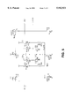
- FIG. 1 shows a schematic of a differential amplifier.
- a current source 102 draws a current from two transistors 104 and 106 which are in parallel. Each transistor has a corresponding resistance 108 and 110 connected between the drain and the supply voltage. The current and the resistances are chosen so that whichever transistor receives the larger gate voltage carries most of the current and the corresponding resistor sustains a voltage drop nearly equal to that of the supply voltage. Hence, if the input voltage VIN is larger than the reference voltage VREF, transistor 106 conducts most of the current drawn by current source 102, and the output voltage VOUT is close to ground. If VIN is supplied from, say, a 2.5V circuit, and transistor 106 is designed using a 1.5V process, then the 2.5V drop between the gate and the drain will cause transistor failure.
- current source 102 An exemplary implementation of current source 102 is shown. Current passing through resistance 112 and transistor 114 self-biases transistor 114. As circuit conditions vary, the temperature coefficient of transistor 114 causes more or less current to be drawn, but this is compensated by the change in gate voltage that results. This provides an accurate bias to transistor 118 with resistance 116 to draw the desired current from transistors 104 and 106. Other current source and current mirror implementations are well known and may be used.
- FIG. 2 shows a schematic of a differential amplifier 202 with protected inputs.
- Differential transistors 104 and 106 receive their input voltages via protection transistors 204 and 206 which have their gates tied to the supply voltage. Input voltages up to the supply voltage VCC minus the threshold voltage VTH are passed to the differential transistors, while voltages higher than that are blocked. Unfortunately, this circuit loses its differential behavior once the reference voltage exceeds VCC-VTH. For an exemplary power supply voltage of 1.5V, a reference voltage of 1.25 V (provided by a 2.5V circuit), would exceed the 1.0V maximum signal level that could be detected. The differential amplifier 202 is then unable to detect a high logic level at VIN.
- a better method for interfacing a reduced voltage circuit to a circuit providing higher voltage signals is therefore desirable.
- the interface would provide for continued differential signal detection at voltage levels exceeding the reduced power supply voltage without requiring that a higher power supply voltage be provided.
- a differential amplifier is provided with a differential input buffer that allows for differential detection even with input voltage signal levels that extend two or more volts beyond the power supply voltage.
- a first transistor and a first resistor coupled in series are coupled in parallel with a second transistor and a second series resistor.
- the transistor drain terminals are both coupled to the power supply voltage, and a current source draws current from the common node of the resistors.
- Input voltages are supplied to the gates of the transistors, and the differential output voltages are provided from the transistor source terminals.
- a differential amplifier receives the differential output voltages and provides a single output voltage.
- the differential buffer transistors are exposed to only the differences between the input voltages and the power supply voltage, and consequently may not be subject to failure if the input voltage exceeds the power supply voltage. Further, the current carrying capacity of the transistors is modulated by the input voltages regardless of whether the input voltages exceed the supply voltages or not, thereby allowing differential detection even with signal voltages that exceed the power supply voltage.
- the differential buffer provides symmetric voltage swings (and for more than a few millivolts, uniform voltage swings) at the input to the differential amplifier, thereby avoiding variable propagation delay issues.
- FIG. 1 is a schematic of a differential amplifier
- FIG. 2 is a schematic of a differential amplifier with protected inputs
- FIG. 3 is a schematic of a differential amplifier with buffered inputs
- FIG. 4 is a schematic of a differential amplifier with a differential buffer
- FIG. 5 is a transistor-level schematic of one embodiment of a differential amplifier having a differential buffer.
- FIG. 3 shows a schematic of a differential amplifier 202 with protected inputs.
- Transistor 302 is coupled in series between the power supply and a resistance 304, and resistance 304 is further coupled to ground.
- An input voltage is provided to the gate of transistor 302, and the ungrounded terminal of resistance 304 is provided as an input to differential amplifier 202.
- This configuration is commonly referred to as a "source follower" configuration.
- a second transistor 306 and a second resistor 308 are also set up in a source follower configuration for the second input to the differential amplifier 202.
- the voltage gain of a source follower is slightly less than 1, with a maximum output voltage of approximately V CC , so the differential amplifier inputs are protected from input voltages which exceed the power supply voltage.
- the source follower transistors 302 and 306 receive input voltages VREF and VIN, respectively. When the input voltages are low, the transistors block current. In this state, the transistors must sustain voltage differences up to the supply voltage, which they are designed to do. When the input voltages are high, the source follower transistors conduct. In this state, the voltage differences sustained by the transistors is the difference between the input voltage and the power supply voltage. Since the transistors are designed to sustain voltage differences at least equal to the power supply voltage, the input voltage may range up to at least twice the power supply voltage without causing transistor failure. In CMOS circuits, care should be taken to avoid driving the chip into SCR latchup, and this may require that a stricter limitation be placed on the input voltages.
- the input voltages may swing by unequal amounts. It is noted that the signal propagation delay in FIG. 3 is strongly influenced the voltage swing, due to the RC time constants caused by the differential amplifier input capacitances and resistors 304 and 308. As a result, the changes in input voltages may propagate to the output voltage at unequal speeds. Both the propagation delay and the shape of the output voltage transition are thereby affected by the input voltage swings. This sensitivity to the input voltage swing magnitude is highly undesirable.
- the differential buffer includes a transistor 402 in series with a resistance 404, coupled in parallel with a second transistor 406 matched to the first (402) and a second resistance 408 equal to the first (404).
- the common node shared by the transistors 402 and 406 is coupled to the supply voltage, and the common node shared by the resistances 404 and 408 is connected to ground via a current source 410.
- the input voltages are provided to the gates of the transistors 402 and 406, and the output voltages are provided to the differential amplifier inputs from the transistor source terminals.
- the differential buffer protects the differential amplifier from excess input signal voltages.
- the differential buffer transistors are can be driven by input voltage signals up to twice the power supply voltage, and the differential configuration of the buffer provides for continued differential signal detection at voltages above the power supply voltage.
- the current source 410 and the resistances 404 and 408 may be chosen so that as long as the difference between the input signal voltages is greater than a few millivolts, the output voltage difference saturates at approximately the power supply voltage.
- the uniform voltage swing at the input to the differential amplifier then provides for a fixed propagation delay, thereby eliminating sensitivity of the output voltage to the size of input voltage swings.
- the current source 410 may be approximated using a large resistance. All of the resistances may be provided in numerous well-known fashions, e.g. by a transistor with a grounded gate. For high frequency operation, the resistances may be replaced with complex impedances.
- FIG. 5 shows a transistor-level schematic of one embodiment of the differential buffer and differential amplifier circuit of FIG. 4. Biasing transistors and current mirrors are shown for completeness, but it is noted that many biasing and current sourcing techniques exist and may be used.
Abstract
Description
Claims (10)
Priority Applications (1)
| Application Number | Priority Date | Filing Date | Title |
|---|---|---|---|
| US08/994,144 US5942921A (en) | 1997-12-19 | 1997-12-19 | Differential comparator with an extended input range |
Applications Claiming Priority (1)
| Application Number | Priority Date | Filing Date | Title |
|---|---|---|---|
| US08/994,144 US5942921A (en) | 1997-12-19 | 1997-12-19 | Differential comparator with an extended input range |
Publications (1)
| Publication Number | Publication Date |
|---|---|
| US5942921A true US5942921A (en) | 1999-08-24 |
Family
ID=25540325
Family Applications (1)
| Application Number | Title | Priority Date | Filing Date |
|---|---|---|---|
| US08/994,144 Expired - Lifetime US5942921A (en) | 1997-12-19 | 1997-12-19 | Differential comparator with an extended input range |
Country Status (1)
| Country | Link |
|---|---|
| US (1) | US5942921A (en) |
Cited By (23)
| Publication number | Priority date | Publication date | Assignee | Title |
|---|---|---|---|---|
| US6215338B1 (en) * | 1998-05-29 | 2001-04-10 | Stmicroelectronics S.R.L. | Monitoring of low currents through a low-side driver DMOS by modulating its internal resistance |
| US6281716B1 (en) * | 1998-07-01 | 2001-08-28 | Mitsubishi Denki Kabushiki Kaisha | Potential detect circuit for detecting whether output potential of potential generation circuit has arrived at target potential or not |
| US6300804B1 (en) | 2000-02-09 | 2001-10-09 | Teradyne, Inc. | Differential comparator with dispersion reduction circuitry |
| US6392448B1 (en) | 2000-02-03 | 2002-05-21 | Teradyne, Inc. | Common-mode detection circuit with cross-coupled compensation |
| US6459556B1 (en) * | 1999-07-22 | 2002-10-01 | Sanyo Electric Co., Ltd. | Input buffer |
| US6586984B1 (en) * | 2002-07-12 | 2003-07-01 | Lsi Logic Corporation | Method for preventing damage to IO devices due to over voltage at pin |
| US20030201799A1 (en) * | 2002-04-26 | 2003-10-30 | Fujitsu Limited | Output circuit capable of transmitting signal with optimal amplitude and optimal common-mode voltage at receiver circuit |
| US6771113B1 (en) * | 2002-02-06 | 2004-08-03 | Lsi Logic Corporation | Five volt tolerant and fail safe input scheme using source follower configuration |
| US6801080B1 (en) | 2003-04-07 | 2004-10-05 | Pericom Semiconductor Corp. | CMOS differential input buffer with source-follower input clamps |
| US6876218B1 (en) * | 2003-02-14 | 2005-04-05 | Xilinx, Inc. | Method for accurate output voltage testing |
| US6888381B2 (en) * | 2001-10-01 | 2005-05-03 | Broadcom Corporation | High speed peak amplitude comparator |
| US6900669B1 (en) * | 2003-08-27 | 2005-05-31 | National Semiconductor Corporation | Area efficient on-chip timeout generator with low temperature and low supply voltage dependency |
| US6940318B1 (en) * | 2003-10-06 | 2005-09-06 | Pericom Semiconductor Corp. | Accurate voltage comparator with voltage-to-current converters for both reference and input voltages |
| US20060012405A1 (en) * | 2004-07-19 | 2006-01-19 | Martins Marcus M | Dual polarity, high input voltage swing comparator using MOS input transistors |
| US20060125529A1 (en) * | 2004-11-22 | 2006-06-15 | Francois Laulanet | Comparator for input voltages higher than supply voltage |
| US20060208768A1 (en) * | 2001-10-02 | 2006-09-21 | Afshin Momtaz | High speed peak amplitude comparator |
| US7276953B1 (en) * | 2003-11-12 | 2007-10-02 | Cypress Semiconductor Corporation | Level shifting input buffer circuit |
| US7808294B1 (en) | 2007-10-15 | 2010-10-05 | Netlogic Microsystems, Inc. | Level shifter with balanced rise and fall times |
| US7956641B1 (en) | 2005-04-28 | 2011-06-07 | Cypress Semiconductor Corporation | Low voltage interface circuit |
| US20110148472A1 (en) * | 2009-12-21 | 2011-06-23 | Oki Semiconductor Co., Ltd. | Voltage change detection device |
| US20140092509A1 (en) * | 2012-09-28 | 2014-04-03 | Fujitsu Semiconductor Limited | Protection circuit, interface circuit, and communication system |
| US9673849B1 (en) | 2016-08-16 | 2017-06-06 | Advanced Micro Devices, Inc. | Common mode extraction and tracking for data signaling |
| US20180026616A1 (en) * | 2016-07-22 | 2018-01-25 | Thine Electronics, Inc. | Input device |
Citations (4)
| Publication number | Priority date | Publication date | Assignee | Title |
|---|---|---|---|---|
| US4295063A (en) * | 1979-06-28 | 1981-10-13 | Motorola Inc. | Fast settling digital to analog converter bit switch |
| US5083046A (en) * | 1989-10-06 | 1992-01-21 | Kabushiki Kaisha Toshiba | Source-coupled fet logic type output circuit |
| US5530444A (en) * | 1995-01-05 | 1996-06-25 | Analog Devices, Inc. | Differential amplifiers which can form a residue amplifier in sub-ranging A/D converters |
| US5541538A (en) * | 1994-09-01 | 1996-07-30 | Harris Corporation | High speed comparator |
-
1997
- 1997-12-19 US US08/994,144 patent/US5942921A/en not_active Expired - Lifetime
Patent Citations (4)
| Publication number | Priority date | Publication date | Assignee | Title |
|---|---|---|---|---|
| US4295063A (en) * | 1979-06-28 | 1981-10-13 | Motorola Inc. | Fast settling digital to analog converter bit switch |
| US5083046A (en) * | 1989-10-06 | 1992-01-21 | Kabushiki Kaisha Toshiba | Source-coupled fet logic type output circuit |
| US5541538A (en) * | 1994-09-01 | 1996-07-30 | Harris Corporation | High speed comparator |
| US5530444A (en) * | 1995-01-05 | 1996-06-25 | Analog Devices, Inc. | Differential amplifiers which can form a residue amplifier in sub-ranging A/D converters |
Cited By (35)
| Publication number | Priority date | Publication date | Assignee | Title |
|---|---|---|---|---|
| US6215338B1 (en) * | 1998-05-29 | 2001-04-10 | Stmicroelectronics S.R.L. | Monitoring of low currents through a low-side driver DMOS by modulating its internal resistance |
| US6281716B1 (en) * | 1998-07-01 | 2001-08-28 | Mitsubishi Denki Kabushiki Kaisha | Potential detect circuit for detecting whether output potential of potential generation circuit has arrived at target potential or not |
| US6459556B1 (en) * | 1999-07-22 | 2002-10-01 | Sanyo Electric Co., Ltd. | Input buffer |
| US6392448B1 (en) | 2000-02-03 | 2002-05-21 | Teradyne, Inc. | Common-mode detection circuit with cross-coupled compensation |
| US6300804B1 (en) | 2000-02-09 | 2001-10-09 | Teradyne, Inc. | Differential comparator with dispersion reduction circuitry |
| US6888381B2 (en) * | 2001-10-01 | 2005-05-03 | Broadcom Corporation | High speed peak amplitude comparator |
| US20060164127A1 (en) * | 2001-10-01 | 2006-07-27 | Broadcom Corporation | High speed peak amplitude comparator |
| US7049856B2 (en) | 2001-10-01 | 2006-05-23 | Broadcom Corporation | High speed peak amplitude comparator |
| US20050122137A1 (en) * | 2001-10-01 | 2005-06-09 | Broadcom Corporation | High speed peak amplitude comparator |
| US20060208768A1 (en) * | 2001-10-02 | 2006-09-21 | Afshin Momtaz | High speed peak amplitude comparator |
| US6771113B1 (en) * | 2002-02-06 | 2004-08-03 | Lsi Logic Corporation | Five volt tolerant and fail safe input scheme using source follower configuration |
| US20030201799A1 (en) * | 2002-04-26 | 2003-10-30 | Fujitsu Limited | Output circuit capable of transmitting signal with optimal amplitude and optimal common-mode voltage at receiver circuit |
| US6870423B2 (en) * | 2002-04-26 | 2005-03-22 | Fujitsu Limited | Output circuit capable of transmitting signal with optimal amplitude and optimal common-mode voltage at receiver circuit |
| US6586984B1 (en) * | 2002-07-12 | 2003-07-01 | Lsi Logic Corporation | Method for preventing damage to IO devices due to over voltage at pin |
| US6876218B1 (en) * | 2003-02-14 | 2005-04-05 | Xilinx, Inc. | Method for accurate output voltage testing |
| US6801080B1 (en) | 2003-04-07 | 2004-10-05 | Pericom Semiconductor Corp. | CMOS differential input buffer with source-follower input clamps |
| US6900669B1 (en) * | 2003-08-27 | 2005-05-31 | National Semiconductor Corporation | Area efficient on-chip timeout generator with low temperature and low supply voltage dependency |
| US6989692B1 (en) * | 2003-10-06 | 2006-01-24 | Pericom Semiconductor Corp. | Substrate-sensing voltage sensor for voltage comparator with voltage-to-current converters for both reference and input voltages |
| US6940318B1 (en) * | 2003-10-06 | 2005-09-06 | Pericom Semiconductor Corp. | Accurate voltage comparator with voltage-to-current converters for both reference and input voltages |
| US7276953B1 (en) * | 2003-11-12 | 2007-10-02 | Cypress Semiconductor Corporation | Level shifting input buffer circuit |
| US20060012405A1 (en) * | 2004-07-19 | 2006-01-19 | Martins Marcus M | Dual polarity, high input voltage swing comparator using MOS input transistors |
| US7233174B2 (en) * | 2004-07-19 | 2007-06-19 | Texas Instruments Incorporated | Dual polarity, high input voltage swing comparator using MOS input transistors |
| US20060125529A1 (en) * | 2004-11-22 | 2006-06-15 | Francois Laulanet | Comparator for input voltages higher than supply voltage |
| US7315187B2 (en) | 2004-11-22 | 2008-01-01 | Ami Semiconductor Belgium Bvba | Comparator for input voltages higher than supply voltage |
| US7956641B1 (en) | 2005-04-28 | 2011-06-07 | Cypress Semiconductor Corporation | Low voltage interface circuit |
| US7808294B1 (en) | 2007-10-15 | 2010-10-05 | Netlogic Microsystems, Inc. | Level shifter with balanced rise and fall times |
| US20110148472A1 (en) * | 2009-12-21 | 2011-06-23 | Oki Semiconductor Co., Ltd. | Voltage change detection device |
| US8653865B2 (en) * | 2009-12-21 | 2014-02-18 | Lapis Semiconductor Co., Ltd. | Voltage change detection device |
| US20140097872A1 (en) * | 2009-12-21 | 2014-04-10 | Lapis Semiconductor Co., Ltd. | Voltage change detection device |
| US8912826B2 (en) * | 2009-12-21 | 2014-12-16 | Lapis Semiconductor Co., Ltd. | Voltage change detection device |
| US20140092509A1 (en) * | 2012-09-28 | 2014-04-03 | Fujitsu Semiconductor Limited | Protection circuit, interface circuit, and communication system |
| US9520708B2 (en) * | 2012-09-28 | 2016-12-13 | Socionext Inc. | Protection circuit, interface circuit, and communication system |
| US20180026616A1 (en) * | 2016-07-22 | 2018-01-25 | Thine Electronics, Inc. | Input device |
| US10250245B2 (en) * | 2016-07-22 | 2019-04-02 | Thine Electronics, Inc. | Input device which outputs a signal having a level corresponding to a state in which a voltage value of an input signal is higher or lower than a threshold value |
| US9673849B1 (en) | 2016-08-16 | 2017-06-06 | Advanced Micro Devices, Inc. | Common mode extraction and tracking for data signaling |
Similar Documents
| Publication | Publication Date | Title |
|---|---|---|
| US5942921A (en) | Differential comparator with an extended input range | |
| US7248115B2 (en) | Differential amplifier operable in wide range | |
| US4477737A (en) | Voltage generator circuit having compensation for process and temperature variation | |
| JP3966016B2 (en) | Clamp circuit | |
| US5107142A (en) | Apparatus for minimizing the reverse bias breakdown of emitter base junction of an output transistor in a tristate bicmos driver circuit | |
| US7157947B2 (en) | Power supplies noise detector for integrated circuits | |
| US5367491A (en) | Apparatus for automatically initiating a stress mode of a semiconductor memory device | |
| JP4328295B2 (en) | Receiver for switched signals on communication lines | |
| EP0887935A1 (en) | Noise isolation circuit | |
| JP2792475B2 (en) | Input buffer | |
| US20030112058A1 (en) | Squelch circuit to create a squelch waveform for USB 2.0 | |
| US6850100B2 (en) | Output buffer circuit | |
| US4296340A (en) | Initializing circuit for MOS integrated circuits | |
| US6037827A (en) | Noise isolation circuit | |
| EP0582289B1 (en) | Transistor circuit for holding peak/bottom level of signal | |
| JPH0685648A (en) | Output circuit | |
| JPH0611102B2 (en) | Signal detection circuit | |
| US20020057106A1 (en) | Data output buffer circuit usable with both PCI and PCI-X buses | |
| US5710516A (en) | Input logic signal buffer circuits | |
| US7281151B2 (en) | Method of stopping data communication of a communication apparatus based on a detection of a power supply voltage drop | |
| JP2003124811A (en) | Clamp circuit | |
| US7164320B2 (en) | Current threshold circuit | |
| JPH05226995A (en) | Power-on reset circuit | |
| US20010013794A1 (en) | Buffer circuit | |
| JP2830480B2 (en) | Semiconductor device |
Legal Events
| Date | Code | Title | Description |
|---|---|---|---|
| AS | Assignment |
Owner name: ADVANCED MICRO DEVICES, INC., CALIFORNIA Free format text: ASSIGNMENT OF ASSIGNORS INTEREST;ASSIGNOR:TALAGA, RONALD F., JR.;REEL/FRAME:008929/0554 Effective date: 19971218 |
|
| STCF | Information on status: patent grant |
Free format text: PATENTED CASE |
|
| FPAY | Fee payment |
Year of fee payment: 4 |
|
| FPAY | Fee payment |
Year of fee payment: 8 |
|
| AS | Assignment |
Owner name: AMD TECHNOLOGIES HOLDINGS, INC., CALIFORNIA Free format text: ASSIGNMENT OF ASSIGNORS INTEREST;ASSIGNOR:ADVANCED MICRO DEVICES, INC.;REEL/FRAME:022764/0488 Effective date: 20090302 Owner name: GLOBALFOUNDRIES INC., CAYMAN ISLANDS Free format text: ASSIGNMENT OF ASSIGNORS INTEREST;ASSIGNOR:AMD TECHNOLOGIES HOLDINGS, INC.;REEL/FRAME:022764/0544 Effective date: 20090302 |
|
| FPAY | Fee payment |
Year of fee payment: 12 |
|
| AS | Assignment |
Owner name: GLOBALFOUNDRIES U.S. INC., NEW YORK Free format text: RELEASE BY SECURED PARTY;ASSIGNOR:WILMINGTON TRUST, NATIONAL ASSOCIATION;REEL/FRAME:056987/0001 Effective date: 20201117 |