US5963832A - Removal of metal cusp for improved contact fill - Google Patents
Removal of metal cusp for improved contact fill Download PDFInfo
- Publication number
- US5963832A US5963832A US09/184,489 US18448998A US5963832A US 5963832 A US5963832 A US 5963832A US 18448998 A US18448998 A US 18448998A US 5963832 A US5963832 A US 5963832A
- Authority
- US
- United States
- Prior art keywords
- contact
- layer
- cusp
- titanium
- conductive layer
- Prior art date
- Legal status (The legal status is an assumption and is not a legal conclusion. Google has not performed a legal analysis and makes no representation as to the accuracy of the status listed.)
- Expired - Lifetime
Links
Images


Classifications
-
- H—ELECTRICITY
- H01—ELECTRIC ELEMENTS
- H01L—SEMICONDUCTOR DEVICES NOT COVERED BY CLASS H10
- H01L21/00—Processes or apparatus adapted for the manufacture or treatment of semiconductor or solid state devices or of parts thereof
- H01L21/70—Manufacture or treatment of devices consisting of a plurality of solid state components formed in or on a common substrate or of parts thereof; Manufacture of integrated circuit devices or of parts thereof
- H01L21/71—Manufacture of specific parts of devices defined in group H01L21/70
- H01L21/768—Applying interconnections to be used for carrying current between separate components within a device comprising conductors and dielectrics
- H01L21/76838—Applying interconnections to be used for carrying current between separate components within a device comprising conductors and dielectrics characterised by the formation and the after-treatment of the conductors
- H01L21/76841—Barrier, adhesion or liner layers
- H01L21/76853—Barrier, adhesion or liner layers characterized by particular after-treatment steps
- H01L21/76865—Selective removal of parts of the layer
-
- H—ELECTRICITY
- H01—ELECTRIC ELEMENTS
- H01L—SEMICONDUCTOR DEVICES NOT COVERED BY CLASS H10
- H01L21/00—Processes or apparatus adapted for the manufacture or treatment of semiconductor or solid state devices or of parts thereof
- H01L21/70—Manufacture or treatment of devices consisting of a plurality of solid state components formed in or on a common substrate or of parts thereof; Manufacture of integrated circuit devices or of parts thereof
- H01L21/71—Manufacture of specific parts of devices defined in group H01L21/70
- H01L21/768—Applying interconnections to be used for carrying current between separate components within a device comprising conductors and dielectrics
- H01L21/76838—Applying interconnections to be used for carrying current between separate components within a device comprising conductors and dielectrics characterised by the formation and the after-treatment of the conductors
- H01L21/76841—Barrier, adhesion or liner layers
- H01L21/76843—Barrier, adhesion or liner layers formed in openings in a dielectric
- H01L21/76844—Bottomless liners
-
- H—ELECTRICITY
- H01—ELECTRIC ELEMENTS
- H01L—SEMICONDUCTOR DEVICES NOT COVERED BY CLASS H10
- H01L21/00—Processes or apparatus adapted for the manufacture or treatment of semiconductor or solid state devices or of parts thereof
- H01L21/70—Manufacture or treatment of devices consisting of a plurality of solid state components formed in or on a common substrate or of parts thereof; Manufacture of integrated circuit devices or of parts thereof
- H01L21/71—Manufacture of specific parts of devices defined in group H01L21/70
- H01L21/768—Applying interconnections to be used for carrying current between separate components within a device comprising conductors and dielectrics
- H01L21/76838—Applying interconnections to be used for carrying current between separate components within a device comprising conductors and dielectrics characterised by the formation and the after-treatment of the conductors
- H01L21/76841—Barrier, adhesion or liner layers
- H01L21/76853—Barrier, adhesion or liner layers characterized by particular after-treatment steps
- H01L21/76855—After-treatment introducing at least one additional element into the layer
-
- H—ELECTRICITY
- H01—ELECTRIC ELEMENTS
- H01L—SEMICONDUCTOR DEVICES NOT COVERED BY CLASS H10
- H01L21/00—Processes or apparatus adapted for the manufacture or treatment of semiconductor or solid state devices or of parts thereof
- H01L21/70—Manufacture or treatment of devices consisting of a plurality of solid state components formed in or on a common substrate or of parts thereof; Manufacture of integrated circuit devices or of parts thereof
- H01L21/71—Manufacture of specific parts of devices defined in group H01L21/70
- H01L21/768—Applying interconnections to be used for carrying current between separate components within a device comprising conductors and dielectrics
- H01L21/76838—Applying interconnections to be used for carrying current between separate components within a device comprising conductors and dielectrics characterised by the formation and the after-treatment of the conductors
- H01L21/76841—Barrier, adhesion or liner layers
- H01L21/76853—Barrier, adhesion or liner layers characterized by particular after-treatment steps
- H01L21/76861—Post-treatment or after-treatment not introducing additional chemical elements into the layer
- H01L21/76862—Bombardment with particles, e.g. treatment in noble gas plasmas; UV irradiation
-
- H—ELECTRICITY
- H01—ELECTRIC ELEMENTS
- H01L—SEMICONDUCTOR DEVICES NOT COVERED BY CLASS H10
- H01L21/00—Processes or apparatus adapted for the manufacture or treatment of semiconductor or solid state devices or of parts thereof
- H01L21/70—Manufacture or treatment of devices consisting of a plurality of solid state components formed in or on a common substrate or of parts thereof; Manufacture of integrated circuit devices or of parts thereof
- H01L21/71—Manufacture of specific parts of devices defined in group H01L21/70
- H01L21/768—Applying interconnections to be used for carrying current between separate components within a device comprising conductors and dielectrics
- H01L21/76838—Applying interconnections to be used for carrying current between separate components within a device comprising conductors and dielectrics characterised by the formation and the after-treatment of the conductors
- H01L21/76841—Barrier, adhesion or liner layers
- H01L21/76853—Barrier, adhesion or liner layers characterized by particular after-treatment steps
- H01L21/76861—Post-treatment or after-treatment not introducing additional chemical elements into the layer
- H01L21/76864—Thermal treatment
-
- H—ELECTRICITY
- H01—ELECTRIC ELEMENTS
- H01L—SEMICONDUCTOR DEVICES NOT COVERED BY CLASS H10
- H01L21/00—Processes or apparatus adapted for the manufacture or treatment of semiconductor or solid state devices or of parts thereof
- H01L21/70—Manufacture or treatment of devices consisting of a plurality of solid state components formed in or on a common substrate or of parts thereof; Manufacture of integrated circuit devices or of parts thereof
- H01L21/71—Manufacture of specific parts of devices defined in group H01L21/70
- H01L21/768—Applying interconnections to be used for carrying current between separate components within a device comprising conductors and dielectrics
- H01L21/76838—Applying interconnections to be used for carrying current between separate components within a device comprising conductors and dielectrics characterised by the formation and the after-treatment of the conductors
- H01L21/76877—Filling of holes, grooves or trenches, e.g. vias, with conductive material
-
- H—ELECTRICITY
- H01—ELECTRIC ELEMENTS
- H01L—SEMICONDUCTOR DEVICES NOT COVERED BY CLASS H10
- H01L23/00—Details of semiconductor or other solid state devices
- H01L23/48—Arrangements for conducting electric current to or from the solid state body in operation, e.g. leads, terminal arrangements ; Selection of materials therefor
- H01L23/482—Arrangements for conducting electric current to or from the solid state body in operation, e.g. leads, terminal arrangements ; Selection of materials therefor consisting of lead-in layers inseparably applied to the semiconductor body
- H01L23/485—Arrangements for conducting electric current to or from the solid state body in operation, e.g. leads, terminal arrangements ; Selection of materials therefor consisting of lead-in layers inseparably applied to the semiconductor body consisting of layered constructions comprising conductive layers and insulating layers, e.g. planar contacts
-
- H—ELECTRICITY
- H01—ELECTRIC ELEMENTS
- H01L—SEMICONDUCTOR DEVICES NOT COVERED BY CLASS H10
- H01L2924/00—Indexing scheme for arrangements or methods for connecting or disconnecting semiconductor or solid-state bodies as covered by H01L24/00
- H01L2924/0001—Technical content checked by a classifier
- H01L2924/0002—Not covered by any one of groups H01L24/00, H01L24/00 and H01L2224/00
Definitions
- the present invention relates to the deposition of conductive layers into contacts to semiconductor substrates, and more particularly to eliminating the formation of voids in filling metal-to-substrate contacts within integrated circuits.
- insulating dielectric layers Multiple line and device levels in an integrated circuit are typically separated by insulating dielectric layers. Contact holes, more simply referred to as “contacts,” are formed through the insulating layers to provide electrical contact between two or more conductive layers.
- the insulating layers must be grown or deposited to a minimum thickness. Too thin an insulating layer results in an intolerably high interlevel capacitance, which ties up otherwise available conduction carriers.
- the contact opening shrinks in size but the depth of the contact (through an insulating layer) must remain the same. In other words, the aspect ratio of contact openings increases as circuitry becomes more densely packed.
- FIG. 1 illustrates a prior art conductive layer 3 deposited into a contact opening 4 to provide the metal-to-metal interlevel electrical contact.
- FIG. 1 is a schematic cross-sectional view, omitting the back wall for simplicity, but that the contact 4 is ordinarily etched in the shape of a cylinder.
- physical vapor deposition of the conductive layer 3, such as metal evaporation or sputtering produces poor step coverage into narrow contact openings having high-aspect ratios.
- metal sputter deposition for example, metal builds quickly on a lip 5 of the contact 4.
- FIG. 1A illustrates a contact made through an insulating layer 16 down to an active area 18 of a semiconductor substrate 20.
- Such contacts are typically even deeper and more narrow than metal-to-metal contacts such as that illustrated in FIG. 1.
- the insulating layer 16 e.g., BPSG
- BPSG BPSG
- the insulating layer 16 is usually very thick in order to provide electrical isolation of underlying devices such as capacitors and transistors.
- Contacts to the substrate in dynamic random access memory (DRAM) cells are particularly deep, as the contact height is dictated by the height of adjacent cell capacitors. DRAM capacitors, in turn, are designed increasingly taller in order to provide adequate surface area for cell capacitance, despite shrinking available real estate.
- DRAM dynamic random access memory
- metal-to-substrate contacts may range in aspect ratio from about 2:1 to 8:1.
- the titanium serves several purposes.
- the titanium at the surface of the silicon may be annealed to form a silicide (TiSi 2 in its stoichiometric form) over the substrate surface.
- the process of forming the silicide (referred to as "silicidation"), further reduces contact resistance by breaking up native oxide (SiO 2 ), an insulator which naturally forms at the silicon surface after the contact is opened.
- the layer of silicide also serves to prevent direct contact between the silicon substrate and tungsten, since tungsten tends to poison the substrate and interfere with electrical operations of transistors and other integrated devices.
- any titanium on the sidewalls of the contact improves adhesion, since CVD tungsten adheres poorly to the insulating layers, such as borophosphosilicate glass (“BPSG”), in which the contact is formed.
- BPSG borophosphosilicate glass
- PVD physical vapor deposition
- sputtering As with the metal-to-metal contact 4 illustrated in FIG. 1, contacts to the substrate 20 also tend to form keyholes or voids during the initial PVD.
- FIG. 1A illustrates the complete blockage of the metal-to-substrate contact 14 caused by titanium (or other PVD metal) deposition.
- the active area 18 represents the bottom of the contact 14.
- a layer 24 often as thick as 1,300 ⁇ to 1,500 ⁇ must be deposited over the insulating layer 16. For higher aspect ratios of future generation circuits, even more titanium must be deposited for sufficient coverage of the bottom.
- the small percentage of metal reaching the active area or substrate surface 18 is due to the natural tendency of PVD to more quickly grow at the corner of the contact hole than elsewhere, forming a metal cusp 26 which extends into the contact opening and eventually pinches it off.
- the thick titanium layer 24 causes the titanium cusp 26 to pinch off, closing the mouth of the contact before enough titanium has reached the substrate.
- the substrate coating 22 is thus too thin.
- the contact 14 must be still be filled with further materials, such as the conventional tungsten plug, even though the contact 14 has been closed off.
- FIGS. 2 and 3 illustrate that, even where the contact 14 is not completely pinched off during deposition of the titanium 22' and 24', the metal cusp 26' is problematic during later contact fill steps.
- FIG. 3 shows the result of a deposition of a CVD tungsten layer 30 and a silicidation step, forming a silicide layer over the substrate surface 18.
- CVD tungsten is generally much more conformal than the PVD titanium 24'. Nevertheless, even the CVD tungsten layer 30 cannot completely fill the contact 14 with such a large cusp 26' shadowing the contact 14, and certainly not if the contact 14 is completely closed off (FIG. 1A).
- a large void 32 thus forms within the plug, reducing the effective size of current flow path for the operational circuit. As aspect ratios of such contacts continually increase with each new generation of microchip, the risk of pinching off the contact opening increases in turn.
- One method of improving step coverage of a PVD metal involves a process of sloping the sidewall of the contact, thus opening the contact in a tapered or cone shape.
- the minimum diameter of the bottom of the contact is still limited by photolithographic resolution. Sloping the contact sidewall thus increases the total area occupied by the contact and reduces the allowable packing density. Such decreases in packing density are unacceptable in the face of current commercial requirements for the miniaturization of integrated circuits.
- a method would also be compatible with conventional physical deposition techniques to allow use of a wide array of metals, including sputtered titanium.
- a method for forming a conductive plug to contact a semiconductor substrate of an integrated circuit.
- the method comprises forming an insulating layer; forming a contact through the insulating layer to expose an active area of the substrate; depositing a first conductive layer over the insulating layer and into the contact; at least partially removing the cusp; and filling the contact with a CVD conductive layer.
- a method for forming electrical contact between layers in an integrated circuit.
- the method comprises opening a contact through an insulating layer to expose a circuit element; depositing an initial conductive layer to form direct contact with a top surface of the insulating layer and the exposed circuit element; and removing a top portion of the initial conductive layer overlying the top surface of the insulating layer.
- a method for forming electrical contact through an insulating layer to a semiconductor substrate.
- the method comprises etching a contact with an aspect ratio of greater than about 2:1 through the insulating layer to the substrate; depositing a metal layer over the insulating layer and into the contact, forming a metal cusp at a lip of the contact; at least partially removing the metal cusp; and depositing a second conductive layer into the contact.
- a method for forming a conductive plug to contact a semiconductor substrate of an integrated circuit.
- the method comprises forming a contact through an insulating layer, to expose an active area of the substrate; depositing a titanium layer over the insulating layer and into the contact; at least partially removing a titanium cusp shadowing the contact; annealing the titanium to form a silicide protective layer over the active area; and depositing a tungsten filler into the contact.
- a method for filling a contact through an insulating layer in an integrated circuit.
- the method comprises depositing an initial conductive layer into the contact and over the insulating layer; mechanically planarizing a top portion of the initial conductive layer; and filling the contact with a second conductive layer after planarizing the top portion.
- a method for forming a conductive contact in an integrated circuit.
- the method comprises forming a contact hole through an insulating layer; forming an initial conductive layer at the bottom of the contact and a top layer over the insulating layer; inverting the structure over an absorbent pad soaked with a viscous etchant to etch the top layer; and depositing a second conductive material into the contact hole after etching the top layer.
- an integrated circuit with a contact plug in electrical contact with a semiconductor substrate comprises an insulating layer with a contact defined by a sidewall and a bottom surface, characterized by an aspect ratio greater than about 2:1; a first metallic layer at least partially lining the contact sidewall; and a conductive filler filling the contact; and a silicide layer interposed between the substrate and the conductive material.
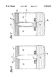
- FIG. 1 is a schematic, partial sectional view of a prior art integrated circuit, showing a metal-to-metal contact.
- FIG. 1A is a schematic, sectional view of a partially fabricated metal-to-substrate contact in an integrated circuit, with the contact mouth pinched off by a sputtered metal.
- FIG. 2 is a schematic, sectional view of a partially fabricated metal-to-substrate contact, like that illustrated in FIG. 1A, but having a small opening through a metal cusp.
- FIG. 3 illustrates the result of a CVD metal deposition into the contact of FIG. 2.
- FIG. 4 is a schematic, partial sectional view of an integrated circuit having a contact opening etched through an insulating layer to expose an active area of a semiconductor substrate, in accordance with a processing stage of the preferred embodiments of the present invention.
- FIG. 5 illustrates the contact of FIG. 4 after an initial PVD metal layer has been deposited over the wafer.
- FIG. 6 illustrates the contact of FIG. 5 after a cusp removal in accordance with a first preferred embodiment of the present invention.
- FIG. 7 illustrates the contact of FIG. 6 after depositing a barrier layer.
- FIG. 8 illustrates the contact of FIG. 7 after a contact fill.
- FIG. 9 illustrates the contact of FIG. 5, with the partially processed circuit inverted over a pad containing a viscous etchant, in accordance with a second preferred embodiment of the present invention.
- FIG. 10 illustrates the contact of FIG. 9 after the PVD metal layer has been partially etched.
- FIG. 11 illustrates the contact of FIG. 10 after further etching.
- FIG. 12 illustrates the contact of FIG. 11 after annealing, depositing a barrier layer, and filling the contact.
- FIG. 13 illustrates the contact of FIG. 11 after an anneal and a contact fill.
- FIG. 14 illustrates the contact of FIG. 5 after a cusp removal, in accordance with a third preferred embodiment of the present invention.
- FIG. 15 illustrates the contact of FIG. 14 after an anneal and a contact fill.
- the present description of the preferred embodiments focuses on contacts between an interconnect layer to be formed and active areas within a silicon substrate, and further focuses on the structure and processes of forming a tungsten plug.
- aspects of the invention may be applied to filling contacts between any two levels in an integrated circuit.
- the invention may be applied to intermetal contacts, such as that illustrated in prior art FIG. 1.
- the skilled artisan will also find application for the present invention wherever good step coverage is desired for a conformal layer in a high-aspect ratio contact.
- DRAM dynamic random access memory
- contacts made to silicon substrates, which are adjacent the DRAM capacitors may range in aspect ratio from about 2:1 to 8:1 and will be even higher for future generation circuits. The contacts are therefore more difficult to conformally fill than are intermetal contacts.
- the contacts of the embodiments described below most preferably range in aspect ratio from about 4:1 to 6:1.
- contacts to the substrate are often filled with a CVD conductive material, such as tungsten.
- a CVD conductive material such as tungsten.
- at least one initial conductive layer is often first deposited for improved contact resistance or diffusion barrier qualities.
- FIG. 4 represents a starting point for the preferred embodiments of the present invention.
- a contact 100 has been opened through a relatively thick insulating layer 102. (It will be understood that the contact 100 generally conforms to a cylindrical shape with a circular shape at the top of the cylindrical opening.)
- the drawings show a cross-sectional view of the contact 100, wherein the back wall is omitted from the views for simplicity.
- the insulating layer 102 which provides electrical isolation for the underlying devices, has a thickness between about 1.0 ⁇ m (micron) and 3.0 ⁇ m, and more preferably between about 1.5 ⁇ m and 2.0 ⁇ m.
- the insulating layer 102 may comprise any suitable dielectric material, but most preferably comprises borophosphosilicate glass ("BPSG").
- BPSG borophosphosilicate glass
- the contact 100 extends down to a surface 104 of a semiconductor substrate 106, which preferably comprises monocrystalline silicon. It will be understood by one of skill in the art of semiconductor processing, however, that the "substrate" in alternative embodiments may comprise other forms of semiconductor layers which include active or operable portions of semiconductor devices.
- the embodiment illustrated in FIG. 4 includes an active area 108 defined in the substrate 106 between two gate electrodes 110. Such an active area may serve as the source or drain of a transistor in a dynamic random access memory (DRAM) chip, for example.
- DRAM dynamic random access memory
- the separation between the gates 110 continues to shrink.
- the separation between gates 110 defines the active area 108, and the active area 108, in turn, defines the (maximum) width of the contact 100.
- the width of the preferred contact may range from about 0.2 ⁇ m to 0.8 ⁇ m, and most preferably about 0.35 ⁇ m, although the contacts of future generations may be even more narrow.
- the contact 100 should have an aspect ratio between about 2:1 and 8:1.
- the aspect ratio is greater than about 4:1 and most preferably greater than about 6:1.
- an initial conductive layer 120 has been formed over the insulating layer 102 and into the contact 100.
- the conductive layer 120 comprises a metal which forms a stable, low-resistance silicide when reacted with silicon. Examples including refractory metals such as titanium, cobalt, tantalum, molybdenum, rhenium, and combinations of such metals.
- the conductive layer 120 of the preferred embodiments comprises titanium.
- a bottom layer or substrate coating 122 of at least about 100 ⁇ of titanium should be formed at the substrate surface 104, at the bottom of the contact 100, and more preferably between about 500 ⁇ and 2,000 ⁇ .
- the conductive layer 120 is formed by a physical vapor deposition ("PVD”), or sputtering. As discussed in the "Background” section above, PVD methods are especially prone to formation of a metal cusp 124 or overhang at the opening of the contact 100.
- PVD physical vapor deposition
- the preferred titanium layer 120 will range in thickness at a top layer 128 (overlying the insulating layer 102) of between about 1,000 ⁇ and 3,000 ⁇ , more preferably between about 1,300 ⁇ and 1,500 ⁇ . As illustrated in FIG. 3 and discussed above, the cusp 124 would ordinarily lead to reliability problems during subsequent deposition steps in the process.
- the initial conductive layer 120 comprises the substrate coating 122, the sidewall portion 126, and the top layer 128.
- the formation of the conductive layer 120 is followed by the contact fill step, whereby a conductive plug is formed.
- the preferred embodiments include some form of a cusp removal step for widening the contact opening and facilitating the later fill step.
- FIGS. 6 through 8 generally illustrate steps of a first preferred embodiment, whereby the cusp removal step comprises planarizing a top portion 128 of the conductive layer 120 by mechanical abrasion.
- mechanical abrasion preferably comprises a standard chemical-mechanical planarization (CMP) step, utilizing a chemically active slurry to aid the mechanical action of a polishing pad.
- CMP chemical-mechanical planarization
- the slurry comprises a silica-based composition.
- the skilled artisan may adapt alternative mechanical abrasion processes to planarize the top layer 128 of the conductive layer 120. By mechanically removing the top portion 128 the cusp 124 is at least partially removed, thus widening the contact opening prior to the next deposition.
- FIG. 6 illustrates the result of the cusp removal step of the first preferred embodiment.
- a least a top portion of the top layer 128 is removed.
- the entire top layer 128 overlying the insulating layer 102 is removed, though less than complete removal of the top portion 128 may still be advantageous in widening the contact opening.
- An upper portion 134 of the insulating layer 102 is preferably also removed, since the preferred mechanical abrasion may also abrade BPSG or any other chosen insulating material.
- a barrier layer 140 is deposited and silicide layer 142 has been formed by an anneal step.
- the anneal preferably comprises heating the structure at between about 600° C. and 900° C., more preferably between about 700° C. and 750° C. for a period between about 20 seconds and 10 minutes.
- a post-silicidation anneal may also be performed at any time before completion of the integrated circuit.
- the second anneal which converts the silicide 142 from the C49 phase to a lower resistance C4 phase, is preferably conducted at between about 650° C. and 800° C.
- the barrier layer 140 may comprise any dense and conductive material, and most preferably comprises titanium nitride deposited by CVD. it will be understood that the barrier layer 140 is not necessary to achieve the advantages of the cusp removal disclosed herein. However, it is preferred in order to prevent later-deposited tungsten of the preferred embodiment from diffusing to the active area 104.
- the barrier layer 140 may also be deposited prior to the mechanical abrasion of the first preferred embodiment. However, the preferred sequence is to deposit the barrier layer 140 after the cusp removal step, since this sequence ensures a better coating of the contact walls after the opening of the contact 100 is widened by the cusp removal step.
- a contact fill step comprising the deposition of a filler material 150, results in a conductive plug 152 filling the contact 14.
- the filler material 150 may comprise any conductive material for which conformal deposition processes are available.
- CVD processes are known for tungsten (W), aluminum (Al), and copper (Cu).
- Other examples include PVD A1, which is forced into the contact at high pressure and temperature (e.g., 600 atm. and 450-500° C.) after deposition.
- tungsten is deposited by a known CVD process.
- the conductive plug 152 is less likely to form troublesome voids.
- the resulting structure may include the barrier layer 140 in direct contact with an upper surface 153 of the insulating layer 102, while the titanium sidewall portion 126 is partially interposed between the filler 150 and the insulating layer 102 within the contact 100.
- the filler material may directly contact the upper surface of the insulating layer.
- the CMP may leave a small amount of the initial conductive layer (e.g., titanium) over the upper surface of the insulating layer.
- FIGS. 9-13 generally illustrate steps of a second preferred embodiment, whereby a viscous etchant at least partially removes the metal cusp 124 generated by the PVD step.
- the wafer of FIG. 5 is first inverted over an absorbent pad 200, which pad contains a viscous etchant.
- viscous the present description means to encompass those etchants with a viscosity higher than about 1.0 mPa-s, and more preferably in the range of about 2 mPa-s to 5 mPa-s.
- the etchant comprises a solution of between about 30% and 60% phosphoric acid, more preferably between about 40% and 50%. Such concentration of phosphoric acid should yield a viscosity between about 2.5 mPa-.s and 3 mPa-s.
- Such viscosity generally permits enough etchant flow to etch the surface of the conductive layer 120 in direct contact with the pad 200. However, the viscosity is not so low as to flow into the contact (through capillary action, for example) and etch the substrate coating 122 or silicide 142, depending upon when the silicidation anneal is carried out.
- the top portion 128 of the initial conductive layer 120 which is in contact with the pad 200, is etched.
- the titanium coating of the sidewall portion 126 and the substrate coating 122 remains unharmed in FIG. 10.
- the temperature during the etch step may range from 0° C. to 100° C. for phosphoric acid, though different temperature ranges may be appropriate depending upon the material characteristics of the chosen etchant.
- FIG. 11 illustrates the result of leaving the wafer inverted over the pad 200 long enough to etch all the titanium overlying the insulating layer 102.
- this may require less than about 10 minutes, preferably between about 2 minutes and 5 minutes.
- the sidewall portion 126 of the initial conductive layer 128 is also partially etched.
- the wafer may be removed from the pad 200 and rinsed of excess etchant in deionized water.
- FIG. 12 shows the wafer of FIG. 11 after an anneal step, a barrier layer deposition, a post-silicidation anneal step, and a contact fill step. These steps may be identical with the corresponding steps of the first preferred embodiment described above.
- a silicide layer 202 is formed; a barrier layer 204, preferably comprising CVD TiN, is formed; and a filler material 206, preferably comprising CVD tungsten, is deposited into the contact 100.
- the above steps need not be performed in the order listed.
- a conductive plug 208 results without voids.
- FIG. 13 An alternative version of the second embodiment is shown in FIG. 13 without a barrier layer, merely to illustrate that the barrier layer 202 of FIG. 12 is optional for all embodiments disclosed herein.
- FIG. 14 illustrates the cusp removal step of a third preferred embodiment of the present invention.
- a facet etch is performed on the structure of FIG. 5 to at least partially remove the cusp 124 of the initial conductive layer 120. Facet etch in general is known in the art, and has been used to slope oxide features within integrated circuits.
- a facet etch on titanium comers over metal-to-metal contacts is disclosed in a copending application of Roberts, et al., entitled “FACET ETCH FOR IMPROVED STEP COVERAGE OF INTEGRATED CIRCUIT CONTACTS,” assigned Ser. No. 08/594,842, filed Jan. 31, 1996, now U.S. Pat. No. 5,730,835.
- the facet etch should be performed by a physical process known as ion beam bombardment, or ion milling.
- High energy ions of a relatively non-reactive chemical preferably a noble gas
- an rf power source creates a plasma condition and argon ions (Ar + ) bombard the wafer within an RIE chamber.
- the etch commonly. known as an argon sputter etch, is enhanced by giving the wafer a negative bias with respect to the plasma.
- the electric field is naturally stronger at the cusp 124 of the initial conductive layer 120, attracting the positive argon ions and leading to preferential etch.
- a sloped facet 300 results, as illustrated in FIG. 14.
- Preferred parameters for the argon sputter etch include an rf power between about 300 and 1,000 W, most preferably about 800 W, a pressure between about 5 and 40 mTorr, most preferably about 15 mTorr, and an argon flow between about 10 and 100 sccm, most preferably about 50 sccm.
- the material removed from the cusp 124 (FIG. 5) of the initial conductive layer 120 also acts as a sputter deposition target, so that at least some of the conductive material of the cusp 124 (FIG. 5) is re-deposited onto sidewalls of the contact 100 to form, in combination with the previous sidewall portion 126 of the initial conductive layer 120, an augmented sidewall portion 302 (FIG. 14).
- the drawings generally represent cross-sectional views of the contact 100 with the back wall omitted for simplicity. It will be understood, however, that material from every point of the cusp 124 all around the mouth of the contact 100 is sputtered to a point diagonally opposite along the contact sidewall, thus forming the augmented sidewall portion 302.
- elemental titanium is etched from the cusp 124 of the initial conductive layer 120, and the titanium is sputtered to the sidewall.
- the augmented sidewall portion 302 provides additional conductive (Ti) coverage of the sidewall, which serves to improve adhesion of the tungsten plug to be deposited.
- FIG. 15 shows the wafer of FIG. 14 after a contact fill with conductive filler material 306.
- the contact fill preferably comprises a CVD step, and most preferably comprises the conformal deposition of tungsten to form a conductive plug 308.
- No barrier layer has been utilized, although it will be understood that a TiN layer may also have been formed prior to the contact fill step, as with the first preferred embodiment.
- the augmented sidewall portion 302 may serve as an extended adhesion layer over the sidewall of insulating layer 102, one of the functions of a barrier layer is already fulfilled.
- the sequence of steps may differ.
- the cusp removal step may be performed at any time prior to a contact fill step.
- multiple cusp removal steps may be performed, with repeated depositions of initial conductive layers therebetween, prior to a fill step. Such a process may be necessary for extremely high-aspect ratio contacts which prevent sufficient Ti from forming at the substrate surface.
Abstract
Description
Claims (17)
Priority Applications (2)
| Application Number | Priority Date | Filing Date | Title |
|---|---|---|---|
| US09/184,489 US5963832A (en) | 1997-06-05 | 1998-11-02 | Removal of metal cusp for improved contact fill |
| US09/334,753 US6423626B1 (en) | 1998-11-02 | 1999-06-16 | Removal of metal cusp for improved contact fill |
Applications Claiming Priority (2)
| Application Number | Priority Date | Filing Date | Title |
|---|---|---|---|
| US08/870,105 US5929526A (en) | 1997-06-05 | 1997-06-05 | Removal of metal cusp for improved contact fill |
| US09/184,489 US5963832A (en) | 1997-06-05 | 1998-11-02 | Removal of metal cusp for improved contact fill |
Related Parent Applications (1)
| Application Number | Title | Priority Date | Filing Date |
|---|---|---|---|
| US08/870,105 Division US5929526A (en) | 1997-06-05 | 1997-06-05 | Removal of metal cusp for improved contact fill |
Related Child Applications (1)
| Application Number | Title | Priority Date | Filing Date |
|---|---|---|---|
| US09/334,753 Division US6423626B1 (en) | 1998-11-02 | 1999-06-16 | Removal of metal cusp for improved contact fill |
Publications (1)
| Publication Number | Publication Date |
|---|---|
| US5963832A true US5963832A (en) | 1999-10-05 |
Family
ID=25354802
Family Applications (2)
| Application Number | Title | Priority Date | Filing Date |
|---|---|---|---|
| US08/870,105 Expired - Lifetime US5929526A (en) | 1997-06-05 | 1997-06-05 | Removal of metal cusp for improved contact fill |
| US09/184,489 Expired - Lifetime US5963832A (en) | 1997-06-05 | 1998-11-02 | Removal of metal cusp for improved contact fill |
Family Applications Before (1)
| Application Number | Title | Priority Date | Filing Date |
|---|---|---|---|
| US08/870,105 Expired - Lifetime US5929526A (en) | 1997-06-05 | 1997-06-05 | Removal of metal cusp for improved contact fill |
Country Status (1)
| Country | Link |
|---|---|
| US (2) | US5929526A (en) |
Cited By (13)
| Publication number | Priority date | Publication date | Assignee | Title |
|---|---|---|---|---|
| US6124203A (en) * | 1998-12-07 | 2000-09-26 | Advanced Micro Devices, Inc. | Method for forming conformal barrier layers |
| WO2002009149A2 (en) * | 2000-07-21 | 2002-01-31 | Motorola, Inc., A Corporation Of The State Of Delaware | Post deposition sputtering |
| US20050032361A1 (en) * | 2001-08-30 | 2005-02-10 | Ammar Derraa | High aspect ratio contact structure with reduced silicon consumption |
| US20060029745A1 (en) * | 1995-06-07 | 2006-02-09 | Sandhu Gurtej S | High throughput ILD fill process for high aspect ratio gap fill |
| US20060202283A1 (en) * | 2001-08-30 | 2006-09-14 | Ammar Deraa | Metal silicide adhesion layer for contact structures |
| US20070049017A1 (en) * | 2005-08-29 | 2007-03-01 | Chao-Ching Hsieh | Plug fabricating method for dielectric layer |
| US20080009133A1 (en) * | 1999-07-22 | 2008-01-10 | Taiwan Semiconductor Manufacturing Company, Ltd. | Sidewall Coverage For Copper Damascene Filling |
| US20080127638A1 (en) * | 2006-12-01 | 2008-06-05 | Marius Vaarkamp | Emission Treatment Systems and Methods |
| US20080141661A1 (en) * | 2006-12-01 | 2008-06-19 | Kenneth Voss | Zone Coated Filter, Emission Treatment Systems and Methods |
| US20090004856A1 (en) * | 2007-06-28 | 2009-01-01 | Hynix Semiconductor Inc. | Method of forming contact plug in semiconductor device |
| US20090158719A1 (en) * | 2007-12-12 | 2009-06-25 | Basf Catalysts Llc | Emission Treatment System |
| US20090288402A1 (en) * | 2007-12-12 | 2009-11-26 | Basf Catalysts Llc | Emission Treatment Catalysts, Systems and Methods |
| US8946087B2 (en) * | 2012-02-02 | 2015-02-03 | Lam Research Corporation | Electroless copper deposition |
Families Citing this family (24)
| Publication number | Priority date | Publication date | Assignee | Title |
|---|---|---|---|---|
| US6686288B1 (en) * | 1996-02-21 | 2004-02-03 | Micron Technology, Inc. | Integrated circuit having self-aligned CVD-tungsten/titanium contact plugs strapped with metal interconnect and method of manufacture |
| US5911113A (en) * | 1997-03-18 | 1999-06-08 | Applied Materials, Inc. | Silicon-doped titanium wetting layer for aluminum plug |
| US5994211A (en) * | 1997-11-21 | 1999-11-30 | Lsi Logic Corporation | Method and composition for reducing gate oxide damage during RF sputter clean |
| US6281121B1 (en) * | 1998-03-06 | 2001-08-28 | Advanced Micro Devices, Inc. | Damascene metal interconnects using highly directional deposition of barrier and/or seed layers including (III) filling metal |
| US6261946B1 (en) * | 1999-01-05 | 2001-07-17 | Advanced Micro Devices, Inc. | Method for forming semiconductor seed layers by high bias deposition |
| US6348709B1 (en) * | 1999-03-15 | 2002-02-19 | Micron Technology, Inc. | Electrical contact for high dielectric constant capacitors and method for fabricating the same |
| JP4807894B2 (en) * | 1999-05-31 | 2011-11-02 | ルネサスエレクトロニクス株式会社 | Semiconductor device |
| US6458416B1 (en) * | 2000-07-19 | 2002-10-01 | Micron Technology, Inc. | Deposition methods |
| US7192888B1 (en) * | 2000-08-21 | 2007-03-20 | Micron Technology, Inc. | Low selectivity deposition methods |
| US7094690B1 (en) | 2000-08-31 | 2006-08-22 | Micron Technology, Inc. | Deposition methods and apparatuses providing surface activation |
| US6649523B2 (en) * | 2000-09-29 | 2003-11-18 | Nutool, Inc. | Method and system to provide material removal and planarization employing a reactive pad |
| US7368014B2 (en) * | 2001-08-09 | 2008-05-06 | Micron Technology, Inc. | Variable temperature deposition methods |
| US7332439B2 (en) * | 2004-09-29 | 2008-02-19 | Intel Corporation | Metal gate transistors with epitaxial source and drain regions |
| US7525197B2 (en) * | 2006-07-31 | 2009-04-28 | Intel Corporation | Barrier process/structure for transistor trench contact applications |
| US7597146B2 (en) * | 2006-10-06 | 2009-10-06 | Halliburton Energy Services, Inc. | Methods and apparatus for completion of well bores |
| JP5596919B2 (en) * | 2008-11-26 | 2014-09-24 | キヤノン株式会社 | Manufacturing method of semiconductor device |
| KR101169167B1 (en) * | 2010-10-25 | 2012-07-30 | 에스케이하이닉스 주식회사 | Semiconductor device and method for forming the same |
| US8699183B2 (en) | 2011-04-22 | 2014-04-15 | Seagate Technology Llc | Write pole and shield with different taper angles |
| US8830625B2 (en) | 2012-11-29 | 2014-09-09 | Seagate Technology Llc | Data writer with tapered side shield sidewalls |
| US9570348B2 (en) * | 2015-05-11 | 2017-02-14 | United Microelectronics Corp. | Method of forming contact strucutre |
| US9691658B1 (en) | 2016-05-19 | 2017-06-27 | Globalfoundries Inc. | Contact fill in an integrated circuit |
| CN109427678B (en) * | 2017-08-24 | 2021-06-08 | 中芯国际集成电路制造(上海)有限公司 | Semiconductor structure and forming method thereof |
| WO2019133027A1 (en) * | 2018-01-01 | 2019-07-04 | Intel Corporation | Quantum dot devices |
| CN114242688A (en) * | 2020-09-09 | 2022-03-25 | 中芯国际集成电路制造(上海)有限公司 | Semiconductor device and method of forming the same |
Citations (31)
| Publication number | Priority date | Publication date | Assignee | Title |
|---|---|---|---|---|
| US4666737A (en) * | 1986-02-11 | 1987-05-19 | Harris Corporation | Via metallization using metal fillets |
| US4792842A (en) * | 1984-07-18 | 1988-12-20 | Hitachi, Ltd. | Semiconductor device with wiring layer using bias sputtering |
| EP0297502A2 (en) * | 1987-06-30 | 1989-01-04 | Hitachi, Ltd. | Method of and apparatus for sputtering |
| JPS6471150A (en) * | 1987-09-11 | 1989-03-16 | Fujitsu Ltd | Manufacture of semiconductor device |
| US4874719A (en) * | 1986-05-06 | 1989-10-17 | Kabushiki Kaisha Toshiba | Method for manufacturing an electrical connection between conductor levels |
| US4963511A (en) * | 1987-11-30 | 1990-10-16 | Texas Instruments Incorporated | Method of reducing tungsten selectivity to a contact sidewall |
| US5066611A (en) * | 1990-08-31 | 1991-11-19 | Micron Technology, Inc. | Method for improving step coverage of a metallization layer on an integrated circuit by use of molybdenum as an anti-reflective coating |
| US5106779A (en) * | 1990-12-06 | 1992-04-21 | Micron Technology, Inc. | Method for widening the laser planarization process window for metalized films on semiconductor wafers |
| US5124780A (en) * | 1991-06-10 | 1992-06-23 | Micron Technology, Inc. | Conductive contact plug and a method of forming a conductive contact plug in an integrated circuit using laser planarization |
| US5147819A (en) * | 1991-02-21 | 1992-09-15 | Micron Technology, Inc. | Semiconductor metallization method |
| US5166093A (en) * | 1991-07-31 | 1992-11-24 | Micron Technology, Inc. | Method to reduce the reflectivity of a semi-conductor metallic surface |
| US5169491A (en) * | 1991-07-29 | 1992-12-08 | Micron Technology, Inc. | Method of etching SiO2 dielectric layers using chemical mechanical polishing techniques |
| US5225034A (en) * | 1992-06-04 | 1993-07-06 | Micron Technology, Inc. | Method of chemical mechanical polishing predominantly copper containing metal layers in semiconductor processing |
| US5278100A (en) * | 1991-11-08 | 1994-01-11 | Micron Technology, Inc. | Chemical vapor deposition technique for depositing titanium silicide on semiconductor wafers |
| US5309023A (en) * | 1989-11-14 | 1994-05-03 | Mitsubishi Denki Kabushiki Kaisha | Contact structure for interconnection in semiconductor devices and manufacturing method thereof |
| US5362666A (en) * | 1992-09-18 | 1994-11-08 | Micron Technology, Inc. | Method of producing a self-aligned contact penetrating cell plate |
| US5376405A (en) * | 1992-08-07 | 1994-12-27 | Micron Technology, Inc. | Chemical vapor deposition technique for depositing titanium silicide on semiconductor wafers |
| US5385867A (en) * | 1993-03-26 | 1995-01-31 | Matsushita Electric Industrial Co., Ltd. | Method for forming a multi-layer metallic wiring structure |
| US5387550A (en) * | 1992-02-07 | 1995-02-07 | Micron Technology, Inc. | Method for making a fillet for integrated circuit metal plug |
| US5416048A (en) * | 1993-04-16 | 1995-05-16 | Micron Semiconductor, Inc. | Method to slope conductor profile prior to dielectric deposition to improve dielectric step-coverage |
| US5420074A (en) * | 1990-07-05 | 1995-05-30 | Kabushiki Kaisha Toshiba | Method for burying low resistance material in a contact hole |
| EP0661736A1 (en) * | 1993-12-28 | 1995-07-05 | Nec Corporation | Method for fabricating multilayer semiconductor device |
| US5444013A (en) * | 1994-11-02 | 1995-08-22 | Micron Technology, Inc. | Method of forming a capacitor |
| US5504038A (en) * | 1995-05-25 | 1996-04-02 | United Microelectronics Corporation | Method for selective tungsten sidewall and bottom contact formation |
| US5545584A (en) * | 1995-07-03 | 1996-08-13 | Taiwan Semiconductor Manufacturing Company | Unified contact plug process for static random access memory (SRAM) having thin film transistors |
| US5580821A (en) * | 1995-02-21 | 1996-12-03 | Micron Technology, Inc. | Semiconductor processing method of forming an electrically conductive contact plug |
| US5644166A (en) * | 1995-07-17 | 1997-07-01 | Micron Technology, Inc. | Sacrificial CVD germanium layer for formation of high aspect ratio submicron VLSI contacts |
| US5654234A (en) * | 1996-04-29 | 1997-08-05 | Taiwan Semiconductor Manufacturing Company, Ltd. | Method for forming a void-free tungsten-plug contact in the presence of a contact opening overhang |
| US5654233A (en) * | 1996-04-08 | 1997-08-05 | Taiwan Semiconductor Manufacturing Company Ltd | Step coverage enhancement process for sub half micron contact/via |
| US5730835A (en) * | 1996-01-31 | 1998-03-24 | Micron Technology, Inc. | Facet etch for improved step coverage of integrated circuit contacts |
| US5833817A (en) * | 1996-04-22 | 1998-11-10 | Taiwan Semiconductor Manufacturing Company, Ltd. | Method for improving conformity and contact bottom coverage of sputtered titanium nitride barrier layers |
-
1997
- 1997-06-05 US US08/870,105 patent/US5929526A/en not_active Expired - Lifetime
-
1998
- 1998-11-02 US US09/184,489 patent/US5963832A/en not_active Expired - Lifetime
Patent Citations (33)
| Publication number | Priority date | Publication date | Assignee | Title |
|---|---|---|---|---|
| US4792842A (en) * | 1984-07-18 | 1988-12-20 | Hitachi, Ltd. | Semiconductor device with wiring layer using bias sputtering |
| US4666737A (en) * | 1986-02-11 | 1987-05-19 | Harris Corporation | Via metallization using metal fillets |
| US4874719A (en) * | 1986-05-06 | 1989-10-17 | Kabushiki Kaisha Toshiba | Method for manufacturing an electrical connection between conductor levels |
| EP0297502A2 (en) * | 1987-06-30 | 1989-01-04 | Hitachi, Ltd. | Method of and apparatus for sputtering |
| JPS6471150A (en) * | 1987-09-11 | 1989-03-16 | Fujitsu Ltd | Manufacture of semiconductor device |
| US4963511A (en) * | 1987-11-30 | 1990-10-16 | Texas Instruments Incorporated | Method of reducing tungsten selectivity to a contact sidewall |
| US5309023A (en) * | 1989-11-14 | 1994-05-03 | Mitsubishi Denki Kabushiki Kaisha | Contact structure for interconnection in semiconductor devices and manufacturing method thereof |
| US5420074A (en) * | 1990-07-05 | 1995-05-30 | Kabushiki Kaisha Toshiba | Method for burying low resistance material in a contact hole |
| US5066611A (en) * | 1990-08-31 | 1991-11-19 | Micron Technology, Inc. | Method for improving step coverage of a metallization layer on an integrated circuit by use of molybdenum as an anti-reflective coating |
| US5106779A (en) * | 1990-12-06 | 1992-04-21 | Micron Technology, Inc. | Method for widening the laser planarization process window for metalized films on semiconductor wafers |
| US5147819A (en) * | 1991-02-21 | 1992-09-15 | Micron Technology, Inc. | Semiconductor metallization method |
| US5124780A (en) * | 1991-06-10 | 1992-06-23 | Micron Technology, Inc. | Conductive contact plug and a method of forming a conductive contact plug in an integrated circuit using laser planarization |
| US5169491A (en) * | 1991-07-29 | 1992-12-08 | Micron Technology, Inc. | Method of etching SiO2 dielectric layers using chemical mechanical polishing techniques |
| US5166093A (en) * | 1991-07-31 | 1992-11-24 | Micron Technology, Inc. | Method to reduce the reflectivity of a semi-conductor metallic surface |
| US5278100A (en) * | 1991-11-08 | 1994-01-11 | Micron Technology, Inc. | Chemical vapor deposition technique for depositing titanium silicide on semiconductor wafers |
| US5387550A (en) * | 1992-02-07 | 1995-02-07 | Micron Technology, Inc. | Method for making a fillet for integrated circuit metal plug |
| US5225034A (en) * | 1992-06-04 | 1993-07-06 | Micron Technology, Inc. | Method of chemical mechanical polishing predominantly copper containing metal layers in semiconductor processing |
| US5354490A (en) * | 1992-06-04 | 1994-10-11 | Micron Technology, Inc. | Slurries for chemical mechanically polishing copper containing metal layers |
| US5376405A (en) * | 1992-08-07 | 1994-12-27 | Micron Technology, Inc. | Chemical vapor deposition technique for depositing titanium silicide on semiconductor wafers |
| US5362666A (en) * | 1992-09-18 | 1994-11-08 | Micron Technology, Inc. | Method of producing a self-aligned contact penetrating cell plate |
| US5385867A (en) * | 1993-03-26 | 1995-01-31 | Matsushita Electric Industrial Co., Ltd. | Method for forming a multi-layer metallic wiring structure |
| US5416048A (en) * | 1993-04-16 | 1995-05-16 | Micron Semiconductor, Inc. | Method to slope conductor profile prior to dielectric deposition to improve dielectric step-coverage |
| EP0661736A1 (en) * | 1993-12-28 | 1995-07-05 | Nec Corporation | Method for fabricating multilayer semiconductor device |
| US5444013A (en) * | 1994-11-02 | 1995-08-22 | Micron Technology, Inc. | Method of forming a capacitor |
| US5580821A (en) * | 1995-02-21 | 1996-12-03 | Micron Technology, Inc. | Semiconductor processing method of forming an electrically conductive contact plug |
| US5504038A (en) * | 1995-05-25 | 1996-04-02 | United Microelectronics Corporation | Method for selective tungsten sidewall and bottom contact formation |
| US5545584A (en) * | 1995-07-03 | 1996-08-13 | Taiwan Semiconductor Manufacturing Company | Unified contact plug process for static random access memory (SRAM) having thin film transistors |
| US5644166A (en) * | 1995-07-17 | 1997-07-01 | Micron Technology, Inc. | Sacrificial CVD germanium layer for formation of high aspect ratio submicron VLSI contacts |
| US5730835A (en) * | 1996-01-31 | 1998-03-24 | Micron Technology, Inc. | Facet etch for improved step coverage of integrated circuit contacts |
| US5861344A (en) * | 1996-01-31 | 1999-01-19 | Micron Technology, Inc. | Facet etch for improved step coverage of integrated circuit contacts |
| US5654233A (en) * | 1996-04-08 | 1997-08-05 | Taiwan Semiconductor Manufacturing Company Ltd | Step coverage enhancement process for sub half micron contact/via |
| US5833817A (en) * | 1996-04-22 | 1998-11-10 | Taiwan Semiconductor Manufacturing Company, Ltd. | Method for improving conformity and contact bottom coverage of sputtered titanium nitride barrier layers |
| US5654234A (en) * | 1996-04-29 | 1997-08-05 | Taiwan Semiconductor Manufacturing Company, Ltd. | Method for forming a void-free tungsten-plug contact in the presence of a contact opening overhang |
Non-Patent Citations (5)
| Title |
|---|
| "Contact Stud Fabrication Process using Dual Ion-Bean Deposition and Etch", Technical Disclosure Bulletin, vol. 29, No. 8, Jan. 1987, pp. 3403-3404. |
| Contact Stud Fabrication Process using Dual Ion Bean Deposition and Etch , Technical Disclosure Bulletin, vol. 29, No. 8, Jan. 1987, pp. 3403 3404. * |
| Homma et al.: "Planarization Mechanism of RF-Biased Al Sputtering", Journal of the Electrochemical Society, vol. 140, No. 3, Mar. 1, 1993, pp. 855-860, XP000378165. |
| Homma et al.: Planarization Mechanism of RF Biased Al Sputtering , Journal of the Electrochemical Society, vol. 140, No. 3, Mar. 1, 1993, pp. 855 860, XP000378165. * |
| Reliable Tungsten Chemical Vapor Deposition Process with Sputter Etch to Form contact Studs:, 700 IBM Technical Disclosure bulleting, vol. 30, No. 10, Mar. 1988, pp. 162/163 XP000111112. * |
Cited By (23)
| Publication number | Priority date | Publication date | Assignee | Title |
|---|---|---|---|---|
| US20060029745A1 (en) * | 1995-06-07 | 2006-02-09 | Sandhu Gurtej S | High throughput ILD fill process for high aspect ratio gap fill |
| US6124203A (en) * | 1998-12-07 | 2000-09-26 | Advanced Micro Devices, Inc. | Method for forming conformal barrier layers |
| US7514348B2 (en) * | 1999-07-22 | 2009-04-07 | Taiwan Semiconductor Manufacturing Company | Sidewall coverage for copper damascene filling |
| US20080009133A1 (en) * | 1999-07-22 | 2008-01-10 | Taiwan Semiconductor Manufacturing Company, Ltd. | Sidewall Coverage For Copper Damascene Filling |
| WO2002009149A3 (en) * | 2000-07-21 | 2002-05-16 | Motorola Inc | Post deposition sputtering |
| WO2002009149A2 (en) * | 2000-07-21 | 2002-01-31 | Motorola, Inc., A Corporation Of The State Of Delaware | Post deposition sputtering |
| US7402512B2 (en) | 2001-08-30 | 2008-07-22 | Micron Technology, Inc. | High aspect ratio contact structure with reduced silicon consumption |
| US20050032361A1 (en) * | 2001-08-30 | 2005-02-10 | Ammar Derraa | High aspect ratio contact structure with reduced silicon consumption |
| US20060202283A1 (en) * | 2001-08-30 | 2006-09-14 | Ammar Deraa | Metal silicide adhesion layer for contact structures |
| US6908849B2 (en) | 2001-08-30 | 2005-06-21 | Micron Technology, Inc. | High aspect ratio contact structure with reduced silicon consumption |
| US20050233577A1 (en) * | 2001-08-30 | 2005-10-20 | Ammar Derraa | High aspect ratio contact structure with reduced silicon consumption |
| US6858904B2 (en) * | 2001-08-30 | 2005-02-22 | Micron Technology, Inc. | High aspect ratio contact structure with reduced silicon consumption |
| US20070049017A1 (en) * | 2005-08-29 | 2007-03-01 | Chao-Ching Hsieh | Plug fabricating method for dielectric layer |
| US20080127638A1 (en) * | 2006-12-01 | 2008-06-05 | Marius Vaarkamp | Emission Treatment Systems and Methods |
| US20080141661A1 (en) * | 2006-12-01 | 2008-06-19 | Kenneth Voss | Zone Coated Filter, Emission Treatment Systems and Methods |
| US8800268B2 (en) | 2006-12-01 | 2014-08-12 | Basf Corporation | Zone coated filter, emission treatment systems and methods |
| US20090004856A1 (en) * | 2007-06-28 | 2009-01-01 | Hynix Semiconductor Inc. | Method of forming contact plug in semiconductor device |
| US20090158719A1 (en) * | 2007-12-12 | 2009-06-25 | Basf Catalysts Llc | Emission Treatment System |
| US20090288402A1 (en) * | 2007-12-12 | 2009-11-26 | Basf Catalysts Llc | Emission Treatment Catalysts, Systems and Methods |
| US9863297B2 (en) | 2007-12-12 | 2018-01-09 | Basf Corporation | Emission treatment system |
| US9993771B2 (en) | 2007-12-12 | 2018-06-12 | Basf Corporation | Emission treatment catalysts, systems and methods |
| US11344845B2 (en) | 2007-12-12 | 2022-05-31 | Basf Corporation | Emission treatment catalysts, systems and methods |
| US8946087B2 (en) * | 2012-02-02 | 2015-02-03 | Lam Research Corporation | Electroless copper deposition |
Also Published As
| Publication number | Publication date |
|---|---|
| US5929526A (en) | 1999-07-27 |
Similar Documents
| Publication | Publication Date | Title |
|---|---|---|
| US5963832A (en) | Removal of metal cusp for improved contact fill | |
| US5730835A (en) | Facet etch for improved step coverage of integrated circuit contacts | |
| US6015749A (en) | Method to improve adhesion between copper and titanium nitride, for copper interconnect structures, via the use of an ion implantation procedure | |
| US6509267B1 (en) | Method of forming low resistance barrier on low k interconnect with electrolessly plated copper seed layer | |
| US6426287B2 (en) | Method for forming a semiconductor connection with a top surface having an enlarged recess | |
| US5472912A (en) | Method of making an integrated circuit structure by using a non-conductive plug | |
| US6800180B1 (en) | Resputtering to achieve better step coverage | |
| US5833817A (en) | Method for improving conformity and contact bottom coverage of sputtered titanium nitride barrier layers | |
| US6265313B1 (en) | Method of manufacturing copper interconnect | |
| US5654234A (en) | Method for forming a void-free tungsten-plug contact in the presence of a contact opening overhang | |
| JPH10189733A (en) | Metal coating method for porous dielectric | |
| US6423626B1 (en) | Removal of metal cusp for improved contact fill | |
| JP2001210647A (en) | Method for forming metallization structure in integrated circuit | |
| US20070252277A1 (en) | Semiconductor devices and fabrication method thereof | |
| US5960314A (en) | Semiconductor processing method of providing an electrically conductive interconnecting plug between an elevationally conductive node and an elevationally outer electrically conductive node | |
| US5899741A (en) | Method of manufacturing low resistance and low junction leakage contact | |
| CN107452674B (en) | Contact fill in integrated circuits | |
| US6215189B1 (en) | Semiconductor device having interconnect layer and method of manufacturing therefor | |
| US5801096A (en) | Self-aligned tungsen etch back process to minimize seams in tungsten plugs | |
| KR20010076659A (en) | Method for fabricating an interconnection layer for semiconductor device | |
| US20030203615A1 (en) | Method for depositing barrier layers in an opening | |
| US5994211A (en) | Method and composition for reducing gate oxide damage during RF sputter clean | |
| US5604659A (en) | Microelectronic device with centered storage capacitor cavity sized less than feature size | |
| US5625231A (en) | Low cost solution to high aspect ratio contact/via adhesion layer application for deep sub-half micrometer back-end-of line technology | |
| US5940726A (en) | Method for forming an electrical contact for embedded memory |
Legal Events
| Date | Code | Title | Description |
|---|---|---|---|
| STCF | Information on status: patent grant |
Free format text: PATENTED CASE |
|
| CC | Certificate of correction | ||
| FEPP | Fee payment procedure |
Free format text: PAYOR NUMBER ASSIGNED (ORIGINAL EVENT CODE: ASPN); ENTITY STATUS OF PATENT OWNER: LARGE ENTITY |
|
| FEPP | Fee payment procedure |
Free format text: PAYOR NUMBER ASSIGNED (ORIGINAL EVENT CODE: ASPN); ENTITY STATUS OF PATENT OWNER: LARGE ENTITY |
|
| FPAY | Fee payment |
Year of fee payment: 4 |
|
| FEPP | Fee payment procedure |
Free format text: PAYER NUMBER DE-ASSIGNED (ORIGINAL EVENT CODE: RMPN); ENTITY STATUS OF PATENT OWNER: LARGE ENTITY Free format text: PAYOR NUMBER ASSIGNED (ORIGINAL EVENT CODE: ASPN); ENTITY STATUS OF PATENT OWNER: LARGE ENTITY |
|
| FPAY | Fee payment |
Year of fee payment: 8 |
|
| FPAY | Fee payment |
Year of fee payment: 12 |
|
| AS | Assignment |
Owner name: U.S. BANK NATIONAL ASSOCIATION, AS COLLATERAL AGENT, CALIFORNIA Free format text: SECURITY INTEREST;ASSIGNOR:MICRON TECHNOLOGY, INC.;REEL/FRAME:038669/0001 Effective date: 20160426 Owner name: U.S. BANK NATIONAL ASSOCIATION, AS COLLATERAL AGEN Free format text: SECURITY INTEREST;ASSIGNOR:MICRON TECHNOLOGY, INC.;REEL/FRAME:038669/0001 Effective date: 20160426 |
|
| AS | Assignment |
Owner name: MORGAN STANLEY SENIOR FUNDING, INC., AS COLLATERAL AGENT, MARYLAND Free format text: PATENT SECURITY AGREEMENT;ASSIGNOR:MICRON TECHNOLOGY, INC.;REEL/FRAME:038954/0001 Effective date: 20160426 Owner name: MORGAN STANLEY SENIOR FUNDING, INC., AS COLLATERAL Free format text: PATENT SECURITY AGREEMENT;ASSIGNOR:MICRON TECHNOLOGY, INC.;REEL/FRAME:038954/0001 Effective date: 20160426 |
|
| AS | Assignment |
Owner name: U.S. BANK NATIONAL ASSOCIATION, AS COLLATERAL AGENT, CALIFORNIA Free format text: CORRECTIVE ASSIGNMENT TO CORRECT THE REPLACE ERRONEOUSLY FILED PATENT #7358718 WITH THE CORRECT PATENT #7358178 PREVIOUSLY RECORDED ON REEL 038669 FRAME 0001. ASSIGNOR(S) HEREBY CONFIRMS THE SECURITY INTEREST;ASSIGNOR:MICRON TECHNOLOGY, INC.;REEL/FRAME:043079/0001 Effective date: 20160426 Owner name: U.S. BANK NATIONAL ASSOCIATION, AS COLLATERAL AGEN Free format text: CORRECTIVE ASSIGNMENT TO CORRECT THE REPLACE ERRONEOUSLY FILED PATENT #7358718 WITH THE CORRECT PATENT #7358178 PREVIOUSLY RECORDED ON REEL 038669 FRAME 0001. ASSIGNOR(S) HEREBY CONFIRMS THE SECURITY INTEREST;ASSIGNOR:MICRON TECHNOLOGY, INC.;REEL/FRAME:043079/0001 Effective date: 20160426 |
|
| AS | Assignment |
Owner name: MICRON TECHNOLOGY, INC., IDAHO Free format text: RELEASE BY SECURED PARTY;ASSIGNOR:U.S. BANK NATIONAL ASSOCIATION, AS COLLATERAL AGENT;REEL/FRAME:047243/0001 Effective date: 20180629 |
|
| AS | Assignment |
Owner name: MICRON TECHNOLOGY, INC., IDAHO Free format text: RELEASE BY SECURED PARTY;ASSIGNOR:MORGAN STANLEY SENIOR FUNDING, INC., AS COLLATERAL AGENT;REEL/FRAME:050937/0001 Effective date: 20190731 |