US5966143A - Data allocation into multiple memories for concurrent access - Google Patents
Data allocation into multiple memories for concurrent access Download PDFInfo
- Publication number
- US5966143A US5966143A US08/949,356 US94935697A US5966143A US 5966143 A US5966143 A US 5966143A US 94935697 A US94935697 A US 94935697A US 5966143 A US5966143 A US 5966143A
- Authority
- US
- United States
- Prior art keywords
- graph
- memory
- computer instructions
- memories
- concurrent access
- Prior art date
- Legal status (The legal status is an assumption and is not a legal conclusion. Google has not performed a legal analysis and makes no representation as to the accuracy of the status listed.)
- Expired - Fee Related
Links
- 230000015654 memory Effects 0.000 title claims abstract description 127
- 238000004040 coloring Methods 0.000 claims abstract description 18
- 238000000638 solvent extraction Methods 0.000 claims abstract description 8
- 238000000034 method Methods 0.000 claims description 40
- 238000012360 testing method Methods 0.000 claims description 13
- 230000009977 dual effect Effects 0.000 claims description 10
- 238000012545 processing Methods 0.000 claims description 5
- 230000001131 transforming effect Effects 0.000 claims 7
- 238000004590 computer program Methods 0.000 claims 1
- 230000010076 replication Effects 0.000 abstract description 10
- 239000003086 colorant Substances 0.000 description 11
- 238000003491 array Methods 0.000 description 8
- 238000010586 diagram Methods 0.000 description 8
- 238000012986 modification Methods 0.000 description 2
- 230000004048 modification Effects 0.000 description 2
- 230000009286 beneficial effect Effects 0.000 description 1
- 238000010276 construction Methods 0.000 description 1
- 230000002708 enhancing effect Effects 0.000 description 1
- 238000005206 flow analysis Methods 0.000 description 1
- 230000003116 impacting effect Effects 0.000 description 1
- 238000005192 partition Methods 0.000 description 1
- 230000004044 response Effects 0.000 description 1
Images


Classifications
-
- G—PHYSICS
- G06—COMPUTING; CALCULATING OR COUNTING
- G06F—ELECTRIC DIGITAL DATA PROCESSING
- G06F8/00—Arrangements for software engineering
- G06F8/40—Transformation of program code
- G06F8/41—Compilation
- G06F8/44—Encoding
- G06F8/441—Register allocation; Assignment of physical memory space to logical memory space
-
- G—PHYSICS
- G06—COMPUTING; CALCULATING OR COUNTING
- G06F—ELECTRIC DIGITAL DATA PROCESSING
- G06F8/00—Arrangements for software engineering
- G06F8/40—Transformation of program code
- G06F8/41—Compilation
- G06F8/44—Encoding
- G06F8/443—Optimisation
Definitions
- the present invention generally relates to compilers, and more specifically to allocating data over multiple memories for concurrent memory accesses.
- DSPs Programmable digital signal processors
- DSPs Programmable digital signal processors
- Data partitioning is currently performed manually by the programmer, who must typically resort to the use of assembler directives or compiler pragmas to control the partitioning of data in a program.
- Automatic data partitioning is therefore becoming a necessity, especially with the current trend towards a heavier reliance on high-level languages to program DSPs. Automatic data partitioning relieves the programmer from this task and helps improve performance across an entire program.
- FIG. 1 is a block diagram of a Digital Signal Processor (DSP) with dual memory banks;
- DSP Digital Signal Processor
- FIG. 2 is an example program that uses multiple concurrent data accesses
- FIG. 3 is a graph that illustrates the concurrent access relationships in the example program shown in FIG. 2;
- FIG. 4 is a block diagram that illustrates allocation of array variables into dual memory banks with replication of one of the variables
- FIG. 5 is a block diagram of a example program for illustrating a concurrent access graph
- FIG. 6 is a concurrent access graph for the example program shown in FIG. 5;
- FIG. 7 is a flowchart illustrating construction of a concurrent access graph
- FIG. 8 is an example program and its associated concurrent access graph illustrating a problem with a variable use reached by two definitions
- FIG. 9 is an example program and its associated concurrent access graph illustrating a problem with a variable definition reaching two uses of that variable
- FIG. 10 is a sample concurrent access graph
- FIG. 11 is a line graph of the sample concurrent access graph shown in FIG. 10;
- FIG. 12 is a concurrent access graph in which a single variable definition reaches two uses of that single variable
- FIG. 13 is a line graph the concurrent access graph shown in FIG. 12 altered by removal of an edge
- FIG. 14 is a flow chart illustrating a method of cost based merging vertices of a line graph
- FIG. 15 is a flow chart illustrating a method of cost based merging vertices of a line graph subject to a maximum memory size constraint
- FIG. 16 is a flow chart illustrating a method of finding a list of merges that cause cycle time reduction as referenced in FIGS. 14 and 15;
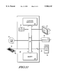
- FIG. 17 is a block diagram illustrating a General Purpose Computer.
- FIG. 1 is a block diagram of a Digital Signal Processor (DSP) with dual memory banks.
- the DSP 100 contains a central processing unit (CPU) 101 coupled to program memory 102 that supplies instructions to the CPU 101, and two data memory banks 103, 104.
- Digital Signal Processors (DSPs) 100 commonly use dual data memory banks to double the memory system's bandwidth. This increases effective memory bandwidth by allowing multiple simultaneous accesses to distinct memory banks. Programmers must assign concurrently-accessed global variables and arrays to different memory banks to achieve performance. Making effective use of dual memory banks is a difficult task, especially for high level language compilers.
- This invention presents a method to perform that task automatically. This method allocates data into multiple memory banks such that concurrent access can be made. This method also automatically selects variables for duplication, enhancing concurrent access opportunities with minimal impact on cost.
- Replication is a technique to enhance concurrent access opportunities.
- arrays A and B are concurrently accessed in one instruction
- array B and C are accessed concurrently in a second instruction
- arrays A and C are accessed concurrently in a third instruction.
- three memory banks are necessary.
- one has duplicate copies of one of the arrays, e.g., array A then all three array accesses may be performed.
- duplication must be made carefully to avoid excessive memory size costs and to avoid overheads for maintaining coherence between multiple copies of the array.
- FIGS. 2, 3 and 4 illustrate this example.
- FIG. 2 is an example program that uses multiple concurrent data accesses.
- FIG. 3 is a graph that illustrates the concurrent access relationships in the example program shown in FIG. 2.
- FIG. 4 is a block diagram that illustrates allocation of array variables into dual memory banks with replication of one of the variables. In FIG. 4, copies of variable A (A 1 and A 2 ) are stored in both memory banks 401, 402.
- the algorithm allocates variables into one of the memory banks. Because memory banks are single-ported, variables that are accessed concurrently, either for reading or writing, by some instruction cannot be allocated in the same memory bank. The requirements for concurrent memory access are generated by the compiler assuming multi-ported memory banks. The goal of the algorithm is to satisfy those access requirements. In case conflict-free allocation is not possible, even after replication, the schedule is altered to perform the memory accesses sequentially instead of concurrently, thus impacting performance.
- FIG. 5 is a block diagram of a example program for illustrating a concurrent access graph. This is a graph that captures all the relationships of concurrent access of the variables in the program.
- FIG. 6 is a concurrent access graph for the example program shown in FIG. 5.
- FIG. 5 illustrates definitions and uses.
- Instruction 1 (501) defines a value for variable a that reaches Instruction 2 (502). In the concurrent access graph (500) this is indicated by an edge labeled "a" between nodes labeled 1 and 2.
- Instruction 1 (501) also defines a value for variable "b” that reaches Instruction 3 (503). Again, in the concurrent access graph (FIG. 6) this is indicated by an edge labeled "b” between nodes labeled 1 and 3.
- FIG. 5 indicates a situation where replication is needed to ensure concurrent access. It this example, one notices that replication of variable "c" would allow for the required concurrent accesses. In this example, extra memory positions (to store the two copies of variable "c") are used to avoid lengthening the schedule and performing the memory accesses sequentially.
- the key idea is to operate on a concurrent access graph that represents concurrent-access constraints.
- a graph-coloring algorithm is applied to the modified graph (This is similar to the graph-coloring representation of access constraints used in optimizing compilers).
- a graph G(V,E) having a set of vertices V corresponding to the instructions in the program and edges E between those instructions is constructed.
- edges labeled X between the instruction containing the STORE and all instructions that contain LOADs of X reached by the STORE. (In compiler terminology, we add an edge between each DEFINITION of variable X and all possible USEs of X).
- Graph G summarizes the requirements for concurrent access: whenever two edges with distinct labels (variable names) share a vertex, it indicates that the corresponding variables must be allocated into different memory banks to allow concurrent access.
- a concurrent access graph G (FIG. 6) is constructed having a vertex for each instruction Mi in the program. If there is a possible execution path in the program such that variable "v" defined at instruction M1 is used as an operand for some operation in instruction M2, Graph G has an edge labeled "v" between vertex M1 and vertex M2.
- Edge coloring of a graph is an assignment of colors to the edges in the graph such that no two edges which have a common vertex are assigned the same color. Each color corresponds to a memory bank. If two variables "X" and "Y" share a vertex in graph G, they are assigned distinct colors and thus located in distinct memory banks. Thus, variables that are concurrently LOADed or STOREd in the same instruction receive different colors by an edge coloring algorithm. Therefore, an allocation created via edge-coloring satisfies the single-ported memory bank constraints, allowing concurrent access from multiple single-ported memory banks as required by the program, provided that the number of colors used is less than or equal to the number of memory banks. If there are more colors than memory banks, this means that the concurrent access requirements cannot be satisfied and the program schedule must be changed by performing some of the accesses sequentially.
- FIG. 9 is an example program and its associated concurrent access graph illustrating a problem with a variable definition reaching two uses of that variable.
- a STORE in instruction "I" 92 reaches two LOADs in instructions "J" 94 and "K” 96, respectively.
- the two corresponding edges would be allocated distinct colors, thus implying in un-necessary replication of the variable.
- FIG. 8 is an example program and its associated concurrent access graph illustrating a problem with a variable use reached by two definitions. There would be an edge from each definition to the use, and each edge would be assigned distinct colors thus generating unnecessary copies. This makes simple edge-coloring method as presented above only applicable for the case of straight line programs. For example, assume that distinct branches of an if-then-else statement assign new values to variable a and the variable is later used at the rejoin. In FIG. 8, the "then" side (Instruction labeled I 82) creates a value for "A" and the "else” since (Instruction labeled J 84) creates a different value.
- FIG. 10 is an example concurrent access graph G.
- FIG. 11 is a line graph L(G) of the example concurrent access graph G shown in FIG. 10.
- the line graph L(G) of a graph G is a graph which has a vertex corresponding to each edge of G. Vertices of L(G) are connected if and only if the corresponding edges of G share a vertex. Vertex-coloring of L(G) corresponds to Edge-coloring of G. (Vertex coloring of a graph G is an assignment of colors to vertices such that no adjacent vertices receive the same color). As before, note that different colors correspond to different memories. Before Vertex Coloring is applied, L(G) is transformed in two ways:
- FIG. 12 is a concurrent access graph G' in which a single variable definition reaches two uses of that single variable.
- FIG. 13 is a line graph L(G') of the concurrent access graph shown in FIG. 12 altered by removal of an edge. This edge removal allows the possibility of all uses of the definition receiving the same color (which implies the variable is stored in one memory bank). However, it is still possible to have distinct colors for each use, which means that the variable might be duplicated, if necessary, to allow concurrent access; and
- L(G') is 2-colorable.
- the Method proceeds by merging those vertices in L(G') that correspond to the same variable. It works in two kinds of vertices:
- the merge is performed as long as 2-colorability is maintained.
- Avoiding a merge may imply duplicating that variable, if distinct edges labeled with that variable name receive different colors, i.e., are assigned to different memory banks.
- Cycle cost refers to program schedule impact of a potential merge. If a variable is replicated, all definitions (STOREs) of that variable must write to all copies of the variable in the memory banks. This may take multiple cycles if the memory ports are otherwise occupied. Similarly, the "bytes" component of the cost refers to the extra memory space required to store the variable in case it is replicated.
- cycle cost of a merge is defined as -1 if all definitions of the variable are found in instructions that have N-1 other memory accesses, where N is the number of memory accesses that can be made concurrently.
- the merge will save one cycle in the execution of the program because, if the variable were replicated, one extra cycle for another memory access would be necessary.
- the cost of a merge is +1 for all other cases.
- the cost of a merge may be set to infinite if the resulting graph after that merge is no longer 2-colorable, for two memory banks, or N-colorable for N memory banks.
- FIG. 14 is a flow chart illustrating a method of cost based merging vertices of a line graph. The method starts by finding minimum cost cycles for L(G'), step 140. These are all the merges that cause a cycle time reduction. Finally, all merges that have a negative cycle cost are performed, step 142.
- FIG. 15 is a flowchart illustrating a method of cost based merging vertices of a line graph subject to a maximum memory size constraint.
- the method starts by finding minimum cost cycles for L(G'), step 140. These are all the merges that cause a cycle time reduction. Then, a cycles/bytes ratio is computed for each potential merge, step 152. The potential merges are then sorted by their cycles/bytes ratios, step 154. A "while" loop is then entered that starts by testing whether a memory threshold has been exceeded, step 156. As long as the memory threshold is not being exceeded, step 156, the potential merge with the smallest cycles/bytes ratio is removed, step 158, and the loop repeats starting with the test at step 156. Otherwise, the method is complete.
- FIG. 16 is a flow chart illustrating a method of finding a list of merges that cause cycle time reduction as referenced in box 140 of FIG. 14 and box 150 of FIG. 15.
- a "while" loop is entered and a check is made for more potential merges, step 160. As long as there are more potential merges, step 160, the loop is executed the next potential merge. Memory and cycle costs are computed for the current potential merge, step 162. Then, a test is made whether the cycle cost is negative, step 164. If the cycle cost is negative, step 164, indicating a potentially beneficial program speedup, the potential merge is added to a list of potential merges, step 166. In either case, regardless of whether the cycle cost is negative, step 164, the loop repeats, starting with the test for more potential merges, step 160. When no more potential merges are found, step 160, the routine is done.
- Edges are weighted by the execution count of the instruction generating the edge.
- profile information one may prioritize concurrent-access inside loops.
- edges generated by instructions inside loops are weighted with the loop nesting depth.
- the algorithm is first applied only considering edges with the highest weight, then successively proceeding to edges of lower weight. It is possible to consider ignoring edges whose weight is below a given threshold. This allows for an algorithmic tradeoff between performance and cost (in memory size) due to data replication.
- FIG. 17 is a block diagram illustrating a General Purpose Computer 20.
- the General Purpose Computer 20 has a Computer Processor 22, and Memory 24, connected by a Bus 26.
- Memory 24 is a relatively high speed machine readable medium and includes Volatile Memories such as DRAM, and SRAM, and Non-Volatile Memories such as, ROM, FLASH, EPROM, EEPROM, and bubble memory.
- Volatile Memories such as DRAM, and SRAM
- Non-Volatile Memories such as, ROM, FLASH, EPROM, EEPROM, and bubble memory.
- Secondary Storage 30 External Storage 32
- output devices such as a monitor 34
- input devices such as a keyboard (with mouse) 36
- printers 38 included in Secondary Storage 30 includes machine readable media such as hard disk drives, magnetic drum, and bubble memory.
- External Storage 32 includes machine readable media such as floppy disks, removable hard drives, magnetic tape, CD-ROM, and even other computers, possibly connected via a communications line.
- Machine readable media such as floppy disks, removable hard drives, magnetic tape, CD-ROM, and even other computers, possibly connected via a communications line.
- the distinction drawn here between Secondary Storage 30 and External Storage 32 is primarily for convenience in describing the invention. As such, it should be appreciated that there is substantial functional overlap between these elements.
- Computer software such as compilers that utilize this invention, compiled code generated by such compiler, and other user programs can be stored in a Computer Software Storage Medium, such as memory 24, Secondary Storage 30, and External Storage 32.
- Non-Volatile Storage Medium such as External Storage 32, Secondary Storage 30, and Non-Volatile Memory and loaded for execution directly into Volatile Memory, executed directly out of Non-Volatile Memory, or stored on the Secondary Storage 30 prior to loading into Volatile Memory for execution.
Abstract
Description
Claims (30)
Priority Applications (1)
| Application Number | Priority Date | Filing Date | Title |
|---|---|---|---|
| US08/949,356 US5966143A (en) | 1997-10-14 | 1997-10-14 | Data allocation into multiple memories for concurrent access |
Applications Claiming Priority (1)
| Application Number | Priority Date | Filing Date | Title |
|---|---|---|---|
| US08/949,356 US5966143A (en) | 1997-10-14 | 1997-10-14 | Data allocation into multiple memories for concurrent access |
Publications (1)
| Publication Number | Publication Date |
|---|---|
| US5966143A true US5966143A (en) | 1999-10-12 |
Family
ID=25488973
Family Applications (1)
| Application Number | Title | Priority Date | Filing Date |
|---|---|---|---|
| US08/949,356 Expired - Fee Related US5966143A (en) | 1997-10-14 | 1997-10-14 | Data allocation into multiple memories for concurrent access |
Country Status (1)
| Country | Link |
|---|---|
| US (1) | US5966143A (en) |
Cited By (38)
| Publication number | Priority date | Publication date | Assignee | Title |
|---|---|---|---|---|
| US6173356B1 (en) * | 1998-02-20 | 2001-01-09 | Silicon Aquarius, Inc. | Multi-port DRAM with integrated SRAM and systems and methods using the same |
| US6446181B1 (en) * | 2000-03-31 | 2002-09-03 | Intel Corporation | System having a configurable cache/SRAM memory |
| US6564303B1 (en) * | 1997-12-31 | 2003-05-13 | Stmicroelectronics S.A. | Dual port memory for digital signal processor |
| US6598221B1 (en) | 2000-04-13 | 2003-07-22 | Koninklijke Philips Electronics N.V. | Assembly code performance evaluation apparatus and method |
| EP1345125A2 (en) * | 2001-12-19 | 2003-09-17 | Agere Systems Inc. | Dynamic random access memory system with bank conflict avoidance feature |
| US6643630B1 (en) | 2000-04-13 | 2003-11-04 | Koninklijke Philips Electronics N.V. | Apparatus and method for annotating an intermediate representation of an application source code |
| US6757795B2 (en) | 2001-04-03 | 2004-06-29 | International Business Machines Corporation | Apparatus and method for efficiently sharing memory bandwidth in a network processor |
| US20050086462A1 (en) * | 2001-03-05 | 2005-04-21 | Martin Vorbach | Methods and devices for treating and/or processing data |
| US7421446B1 (en) * | 2004-08-25 | 2008-09-02 | Unisys Corporation | Allocation of storage for a database |
| US7650448B2 (en) | 1996-12-20 | 2010-01-19 | Pact Xpp Technologies Ag | I/O and memory bus system for DFPS and units with two- or multi-dimensional programmable cell architectures |
| US7657861B2 (en) | 2002-08-07 | 2010-02-02 | Pact Xpp Technologies Ag | Method and device for processing data |
| US7657877B2 (en) | 2001-06-20 | 2010-02-02 | Pact Xpp Technologies Ag | Method for processing data |
| US7782087B2 (en) | 2002-09-06 | 2010-08-24 | Martin Vorbach | Reconfigurable sequencer structure |
| US7822881B2 (en) | 1996-12-27 | 2010-10-26 | Martin Vorbach | Process for automatic dynamic reloading of data flow processors (DFPs) and units with two- or three-dimensional programmable cell architectures (FPGAs, DPGAs, and the like) |
| US7822968B2 (en) | 1996-12-09 | 2010-10-26 | Martin Vorbach | Circuit having a multidimensional structure of configurable cells that include multi-bit-wide inputs and outputs |
| US7840842B2 (en) | 2001-09-03 | 2010-11-23 | Martin Vorbach | Method for debugging reconfigurable architectures |
| US7844796B2 (en) | 2001-03-05 | 2010-11-30 | Martin Vorbach | Data processing device and method |
| US7996361B1 (en) * | 2003-06-30 | 2011-08-09 | Symantec Operating Corporation | Method and system of providing replica files within a fileset |
| US7996827B2 (en) | 2001-08-16 | 2011-08-09 | Martin Vorbach | Method for the translation of programs for reconfigurable architectures |
| US8058899B2 (en) | 2000-10-06 | 2011-11-15 | Martin Vorbach | Logic cell array and bus system |
| US8099618B2 (en) | 2001-03-05 | 2012-01-17 | Martin Vorbach | Methods and devices for treating and processing data |
| US8127061B2 (en) | 2002-02-18 | 2012-02-28 | Martin Vorbach | Bus systems and reconfiguration methods |
| US8156284B2 (en) | 2002-08-07 | 2012-04-10 | Martin Vorbach | Data processing method and device |
| US8209653B2 (en) | 2001-09-03 | 2012-06-26 | Martin Vorbach | Router |
| US8230411B1 (en) | 1999-06-10 | 2012-07-24 | Martin Vorbach | Method for interleaving a program over a plurality of cells |
| US8250503B2 (en) | 2006-01-18 | 2012-08-21 | Martin Vorbach | Hardware definition method including determining whether to implement a function as hardware or software |
| US8281108B2 (en) | 2002-01-19 | 2012-10-02 | Martin Vorbach | Reconfigurable general purpose processor having time restricted configurations |
| US8301872B2 (en) | 2000-06-13 | 2012-10-30 | Martin Vorbach | Pipeline configuration protocol and configuration unit communication |
| USRE44365E1 (en) | 1997-02-08 | 2013-07-09 | Martin Vorbach | Method of self-synchronization of configurable elements of a programmable module |
| US8686475B2 (en) | 2001-09-19 | 2014-04-01 | Pact Xpp Technologies Ag | Reconfigurable elements |
| US8686549B2 (en) | 2001-09-03 | 2014-04-01 | Martin Vorbach | Reconfigurable elements |
| US8812820B2 (en) | 2003-08-28 | 2014-08-19 | Pact Xpp Technologies Ag | Data processing device and method |
| US8819505B2 (en) | 1997-12-22 | 2014-08-26 | Pact Xpp Technologies Ag | Data processor having disabled cores |
| US8914590B2 (en) | 2002-08-07 | 2014-12-16 | Pact Xpp Technologies Ag | Data processing method and device |
| US9037807B2 (en) | 2001-03-05 | 2015-05-19 | Pact Xpp Technologies Ag | Processor arrangement on a chip including data processing, memory, and interface elements |
| GB2582785A (en) * | 2019-04-02 | 2020-10-07 | Graphcore Ltd | Compiling a program from a graph |
| US10817493B2 (en) | 2017-07-07 | 2020-10-27 | Raytheon Company | Data interpolation |
| US11385700B2 (en) * | 2019-02-07 | 2022-07-12 | Fujitsu Limited | Estimation of power consumption for a job based on adjusted calculation of similarities between jobs |
Citations (4)
| Publication number | Priority date | Publication date | Assignee | Title |
|---|---|---|---|---|
| US4571678A (en) * | 1982-11-05 | 1986-02-18 | International Business Machines Corporation | Register allocation and spilling via graph coloring |
| US5249295A (en) * | 1990-06-20 | 1993-09-28 | Rice University | Digital computer register allocation and code spilling using interference graph coloring |
| US5418958A (en) * | 1992-07-15 | 1995-05-23 | Sun Microsystems, Inc. | Register allocation by decomposing, re-connecting and coloring hierarchical program regions |
| US5774730A (en) * | 1995-07-31 | 1998-06-30 | International Business Machines Corporation | Method and apparatus for improving colorability of constrained nodes in an interference graph within a computer system |
-
1997
- 1997-10-14 US US08/949,356 patent/US5966143A/en not_active Expired - Fee Related
Patent Citations (4)
| Publication number | Priority date | Publication date | Assignee | Title |
|---|---|---|---|---|
| US4571678A (en) * | 1982-11-05 | 1986-02-18 | International Business Machines Corporation | Register allocation and spilling via graph coloring |
| US5249295A (en) * | 1990-06-20 | 1993-09-28 | Rice University | Digital computer register allocation and code spilling using interference graph coloring |
| US5418958A (en) * | 1992-07-15 | 1995-05-23 | Sun Microsystems, Inc. | Register allocation by decomposing, re-connecting and coloring hierarchical program regions |
| US5774730A (en) * | 1995-07-31 | 1998-06-30 | International Business Machines Corporation | Method and apparatus for improving colorability of constrained nodes in an interference graph within a computer system |
Non-Patent Citations (10)
| Title |
|---|
| Ashok Sudarsanam, et al., "Memory Bank and Register Allocation in Software Synthesis for ASIPs", Department of Electrical Engineering, Princeton University, 5 pgs. |
| Ashok Sudarsanam, et al., Memory Bank and Register Allocation in Software Synthesis for ASIPs , Department of Electrical Engineering, Princeton University, 5 pgs. * |
| Briggs Cooper Torczon, Improvements to Graph Coloring Register Allocation, ACM Transactions on Programming Languages and Systems, vol. 16, No. 3, pp. 428 455, May 1994. * |
| Briggs-Cooper-Torczon, "Improvements to Graph Coloring Register Allocation," ACM Transactions on Programming Languages and Systems, vol. 16, No. 3, pp. 428-455, May 1994. |
| Mauricio Breternitz, et al., "Implementation Optimization Techniques for Architecture Synthesis of Application-Specific Processors", 1991 ACM 0-89791-460-091/0011/0114, pp. 114-123. |
| Mauricio Breternitz, et al., Implementation Optimization Techniques for Architecture Synthesis of Application Specific Processors , 1991 ACM 0 89791 460 091/0011/0114, pp. 114 123. * |
| Mauricio Breternitz, Jr & John Paul Shen, Implementation Optimization Techniques for Architecture Synthesis of Application Specific Processors, ACM, Nov. 1991. * |
| Mauricio Breternitz, Jr & John Paul Shen, Implementation Optimization Techniques for Architecture Synthesis of Application-Specific Processors, ACM, Nov. 1991. |
| Mazen A.R. Saghir, et al., "Automatic Data Partitioning for HLL DSP Compilers", Dept. of Electrical and Computer Engineering, University of Toronto, Canada, pp. 1-6. |
| Mazen A.R. Saghir, et al., Automatic Data Partitioning for HLL DSP Compilers , Dept. of Electrical and Computer Engineering, University of Toronto, Canada, pp. 1 6. * |
Cited By (63)
| Publication number | Priority date | Publication date | Assignee | Title |
|---|---|---|---|---|
| US8156312B2 (en) | 1996-12-09 | 2012-04-10 | Martin Vorbach | Processor chip for reconfigurable data processing, for processing numeric and logic operations and including function and interconnection control units |
| US7822968B2 (en) | 1996-12-09 | 2010-10-26 | Martin Vorbach | Circuit having a multidimensional structure of configurable cells that include multi-bit-wide inputs and outputs |
| US7650448B2 (en) | 1996-12-20 | 2010-01-19 | Pact Xpp Technologies Ag | I/O and memory bus system for DFPS and units with two- or multi-dimensional programmable cell architectures |
| US8195856B2 (en) | 1996-12-20 | 2012-06-05 | Martin Vorbach | I/O and memory bus system for DFPS and units with two- or multi-dimensional programmable cell architectures |
| US7899962B2 (en) | 1996-12-20 | 2011-03-01 | Martin Vorbach | I/O and memory bus system for DFPs and units with two- or multi-dimensional programmable cell architectures |
| US7822881B2 (en) | 1996-12-27 | 2010-10-26 | Martin Vorbach | Process for automatic dynamic reloading of data flow processors (DFPs) and units with two- or three-dimensional programmable cell architectures (FPGAs, DPGAs, and the like) |
| USRE44383E1 (en) | 1997-02-08 | 2013-07-16 | Martin Vorbach | Method of self-synchronization of configurable elements of a programmable module |
| USRE44365E1 (en) | 1997-02-08 | 2013-07-09 | Martin Vorbach | Method of self-synchronization of configurable elements of a programmable module |
| USRE45109E1 (en) | 1997-02-08 | 2014-09-02 | Pact Xpp Technologies Ag | Method of self-synchronization of configurable elements of a programmable module |
| USRE45223E1 (en) | 1997-02-08 | 2014-10-28 | Pact Xpp Technologies Ag | Method of self-synchronization of configurable elements of a programmable module |
| US8819505B2 (en) | 1997-12-22 | 2014-08-26 | Pact Xpp Technologies Ag | Data processor having disabled cores |
| US6564303B1 (en) * | 1997-12-31 | 2003-05-13 | Stmicroelectronics S.A. | Dual port memory for digital signal processor |
| US6173356B1 (en) * | 1998-02-20 | 2001-01-09 | Silicon Aquarius, Inc. | Multi-port DRAM with integrated SRAM and systems and methods using the same |
| US8468329B2 (en) | 1999-02-25 | 2013-06-18 | Martin Vorbach | Pipeline configuration protocol and configuration unit communication |
| US8312200B2 (en) | 1999-06-10 | 2012-11-13 | Martin Vorbach | Processor chip including a plurality of cache elements connected to a plurality of processor cores |
| US8726250B2 (en) | 1999-06-10 | 2014-05-13 | Pact Xpp Technologies Ag | Configurable logic integrated circuit having a multidimensional structure of configurable elements |
| US8230411B1 (en) | 1999-06-10 | 2012-07-24 | Martin Vorbach | Method for interleaving a program over a plurality of cells |
| US6446181B1 (en) * | 2000-03-31 | 2002-09-03 | Intel Corporation | System having a configurable cache/SRAM memory |
| US6643630B1 (en) | 2000-04-13 | 2003-11-04 | Koninklijke Philips Electronics N.V. | Apparatus and method for annotating an intermediate representation of an application source code |
| US6598221B1 (en) | 2000-04-13 | 2003-07-22 | Koninklijke Philips Electronics N.V. | Assembly code performance evaluation apparatus and method |
| US8301872B2 (en) | 2000-06-13 | 2012-10-30 | Martin Vorbach | Pipeline configuration protocol and configuration unit communication |
| US9047440B2 (en) | 2000-10-06 | 2015-06-02 | Pact Xpp Technologies Ag | Logical cell array and bus system |
| US8471593B2 (en) | 2000-10-06 | 2013-06-25 | Martin Vorbach | Logic cell array and bus system |
| US8058899B2 (en) | 2000-10-06 | 2011-11-15 | Martin Vorbach | Logic cell array and bus system |
| US20050086462A1 (en) * | 2001-03-05 | 2005-04-21 | Martin Vorbach | Methods and devices for treating and/or processing data |
| US7844796B2 (en) | 2001-03-05 | 2010-11-30 | Martin Vorbach | Data processing device and method |
| US8145881B2 (en) | 2001-03-05 | 2012-03-27 | Martin Vorbach | Data processing device and method |
| US9037807B2 (en) | 2001-03-05 | 2015-05-19 | Pact Xpp Technologies Ag | Processor arrangement on a chip including data processing, memory, and interface elements |
| US8312301B2 (en) | 2001-03-05 | 2012-11-13 | Martin Vorbach | Methods and devices for treating and processing data |
| US9075605B2 (en) | 2001-03-05 | 2015-07-07 | Pact Xpp Technologies Ag | Methods and devices for treating and processing data |
| US8099618B2 (en) | 2001-03-05 | 2012-01-17 | Martin Vorbach | Methods and devices for treating and processing data |
| US6757795B2 (en) | 2001-04-03 | 2004-06-29 | International Business Machines Corporation | Apparatus and method for efficiently sharing memory bandwidth in a network processor |
| US7657877B2 (en) | 2001-06-20 | 2010-02-02 | Pact Xpp Technologies Ag | Method for processing data |
| US7996827B2 (en) | 2001-08-16 | 2011-08-09 | Martin Vorbach | Method for the translation of programs for reconfigurable architectures |
| US8869121B2 (en) | 2001-08-16 | 2014-10-21 | Pact Xpp Technologies Ag | Method for the translation of programs for reconfigurable architectures |
| US8407525B2 (en) | 2001-09-03 | 2013-03-26 | Pact Xpp Technologies Ag | Method for debugging reconfigurable architectures |
| US8069373B2 (en) | 2001-09-03 | 2011-11-29 | Martin Vorbach | Method for debugging reconfigurable architectures |
| US8686549B2 (en) | 2001-09-03 | 2014-04-01 | Martin Vorbach | Reconfigurable elements |
| US8209653B2 (en) | 2001-09-03 | 2012-06-26 | Martin Vorbach | Router |
| US7840842B2 (en) | 2001-09-03 | 2010-11-23 | Martin Vorbach | Method for debugging reconfigurable architectures |
| US8429385B2 (en) | 2001-09-03 | 2013-04-23 | Martin Vorbach | Device including a field having function cells and information providing cells controlled by the function cells |
| US8686475B2 (en) | 2001-09-19 | 2014-04-01 | Pact Xpp Technologies Ag | Reconfigurable elements |
| KR100963721B1 (en) | 2001-12-19 | 2010-06-14 | 에이저 시스템즈 인크 | Dynamic random access memory system with bank conflict avoidance feature |
| EP1345125A2 (en) * | 2001-12-19 | 2003-09-17 | Agere Systems Inc. | Dynamic random access memory system with bank conflict avoidance feature |
| EP1345125A3 (en) * | 2001-12-19 | 2007-04-04 | Agere Systems Inc. | Dynamic random access memory system with bank conflict avoidance feature |
| US8281108B2 (en) | 2002-01-19 | 2012-10-02 | Martin Vorbach | Reconfigurable general purpose processor having time restricted configurations |
| US8127061B2 (en) | 2002-02-18 | 2012-02-28 | Martin Vorbach | Bus systems and reconfiguration methods |
| US8156284B2 (en) | 2002-08-07 | 2012-04-10 | Martin Vorbach | Data processing method and device |
| US8914590B2 (en) | 2002-08-07 | 2014-12-16 | Pact Xpp Technologies Ag | Data processing method and device |
| US8281265B2 (en) | 2002-08-07 | 2012-10-02 | Martin Vorbach | Method and device for processing data |
| US7657861B2 (en) | 2002-08-07 | 2010-02-02 | Pact Xpp Technologies Ag | Method and device for processing data |
| US7928763B2 (en) | 2002-09-06 | 2011-04-19 | Martin Vorbach | Multi-core processing system |
| US8803552B2 (en) | 2002-09-06 | 2014-08-12 | Pact Xpp Technologies Ag | Reconfigurable sequencer structure |
| US8310274B2 (en) | 2002-09-06 | 2012-11-13 | Martin Vorbach | Reconfigurable sequencer structure |
| US7782087B2 (en) | 2002-09-06 | 2010-08-24 | Martin Vorbach | Reconfigurable sequencer structure |
| US7996361B1 (en) * | 2003-06-30 | 2011-08-09 | Symantec Operating Corporation | Method and system of providing replica files within a fileset |
| US8812820B2 (en) | 2003-08-28 | 2014-08-19 | Pact Xpp Technologies Ag | Data processing device and method |
| US7421446B1 (en) * | 2004-08-25 | 2008-09-02 | Unisys Corporation | Allocation of storage for a database |
| US8250503B2 (en) | 2006-01-18 | 2012-08-21 | Martin Vorbach | Hardware definition method including determining whether to implement a function as hardware or software |
| US10817493B2 (en) | 2017-07-07 | 2020-10-27 | Raytheon Company | Data interpolation |
| US11385700B2 (en) * | 2019-02-07 | 2022-07-12 | Fujitsu Limited | Estimation of power consumption for a job based on adjusted calculation of similarities between jobs |
| GB2582785A (en) * | 2019-04-02 | 2020-10-07 | Graphcore Ltd | Compiling a program from a graph |
| US11720332B2 (en) | 2019-04-02 | 2023-08-08 | Graphcore Limited | Compiling a program from a graph |
Similar Documents
| Publication | Publication Date | Title |
|---|---|---|
| US5966143A (en) | Data allocation into multiple memories for concurrent access | |
| Hansen | Operating system principles | |
| Goguen et al. | Concurrent term rewriting as a model of computation | |
| US8627018B2 (en) | Automatic optimization for programming of many-core architectures | |
| US20120151182A1 (en) | Performing Function Calls Using Single Instruction Multiple Data (SIMD) Registers | |
| US6446258B1 (en) | Interactive instruction scheduling and block ordering | |
| EP1785875A2 (en) | Method for mapping applications on a multiprocessor platform/system | |
| EP0735468A2 (en) | Method and apparatus for an optimizing compiler | |
| CN101681294A (en) | Memory transaction grouping | |
| CN103348323A (en) | Dynamic binary optimization | |
| JPH06103463B2 (en) | Code generation method | |
| US20080005722A1 (en) | Compiling device, compiling method and recording medium | |
| CN100362474C (en) | Time-multiplexed speculative multi-threading to support single-threaded applications | |
| Kessler | Scheduling expression DAGs for minimal register need | |
| US7356812B2 (en) | Passing parameters by implicit reference | |
| US7779230B2 (en) | Data flow execution of methods in sequential programs | |
| EP0514763A2 (en) | A data processor having a logical register content-addressable memory | |
| KR20150101870A (en) | Method and apparatus for avoiding bank conflict in memory | |
| Hascoët et al. | Programming language features, usage patterns, and the efficiency of generated adjoint code | |
| US20060002224A1 (en) | Bank assignment for partitioned register banks | |
| US5848275A (en) | Compiler having automatic common blocks of memory splitting | |
| Potasman | Percolation-based compiling for evaluation of parallelism and hardware design trade-offs | |
| US20060095743A1 (en) | Vliw processor with copy register file | |
| US11762641B2 (en) | Allocating variables to computer memory | |
| Leeman et al. | Automated dynamic memory data type implementation exploration and optimization |
Legal Events
| Date | Code | Title | Description |
|---|---|---|---|
| AS | Assignment |
Owner name: KEYBOARD KOMFORT, INC., MICHIGAN Free format text: ASSIGNMENT OF ASSIGNORS INTEREST;ASSIGNOR:ALDRICH, STEVEN H.;REEL/FRAME:008798/0326 Effective date: 19971010 |
|
| AS | Assignment |
Owner name: MOTOROLA, INC., ILLINOIS Free format text: ASSIGNMENT OF ASSIGNORS INTEREST;ASSIGNOR:BRETERNITZ, MAURICIO JR.;REEL/FRAME:008775/0980 Effective date: 19971009 |
|
| FPAY | Fee payment |
Year of fee payment: 4 |
|
| AS | Assignment |
Owner name: FREESCALE SEMICONDUCTOR, INC., TEXAS Free format text: ASSIGNMENT OF ASSIGNORS INTEREST;ASSIGNOR:MOTOROLA, INC.;REEL/FRAME:015698/0657 Effective date: 20040404 Owner name: FREESCALE SEMICONDUCTOR, INC.,TEXAS Free format text: ASSIGNMENT OF ASSIGNORS INTEREST;ASSIGNOR:MOTOROLA, INC.;REEL/FRAME:015698/0657 Effective date: 20040404 |
|
| AS | Assignment |
Owner name: CITIBANK, N.A. AS COLLATERAL AGENT, NEW YORK Free format text: SECURITY AGREEMENT;ASSIGNORS:FREESCALE SEMICONDUCTOR, INC.;FREESCALE ACQUISITION CORPORATION;FREESCALE ACQUISITION HOLDINGS CORP.;AND OTHERS;REEL/FRAME:018855/0129 Effective date: 20061201 Owner name: CITIBANK, N.A. AS COLLATERAL AGENT,NEW YORK Free format text: SECURITY AGREEMENT;ASSIGNORS:FREESCALE SEMICONDUCTOR, INC.;FREESCALE ACQUISITION CORPORATION;FREESCALE ACQUISITION HOLDINGS CORP.;AND OTHERS;REEL/FRAME:018855/0129 Effective date: 20061201 |
|
| REMI | Maintenance fee reminder mailed | ||
| LAPS | Lapse for failure to pay maintenance fees | ||
| STCH | Information on status: patent discontinuation |
Free format text: PATENT EXPIRED DUE TO NONPAYMENT OF MAINTENANCE FEES UNDER 37 CFR 1.362 |
|
| FP | Lapsed due to failure to pay maintenance fee |
Effective date: 20071012 |
|
| AS | Assignment |
Owner name: FREESCALE SEMICONDUCTOR, INC., TEXAS Free format text: PATENT RELEASE;ASSIGNOR:CITIBANK, N.A., AS COLLATERAL AGENT;REEL/FRAME:037354/0225 Effective date: 20151207 |