US5984746A - Attaching spacers in a display device - Google Patents
Attaching spacers in a display device Download PDFInfo
- Publication number
- US5984746A US5984746A US08/764,485 US76448596A US5984746A US 5984746 A US5984746 A US 5984746A US 76448596 A US76448596 A US 76448596A US 5984746 A US5984746 A US 5984746A
- Authority
- US
- United States
- Prior art keywords
- mixture
- faceplate
- grille
- spacers
- conductive layer
- Prior art date
- Legal status (The legal status is an assumption and is not a legal conclusion. Google has not performed a legal analysis and makes no representation as to the accuracy of the status listed.)
- Expired - Fee Related
Links
- 125000006850 spacer group Chemical group 0.000 title claims abstract description 34
- 239000000203 mixture Substances 0.000 claims abstract description 54
- 238000000034 method Methods 0.000 claims abstract description 26
- 229920002120 photoresistant polymer Polymers 0.000 claims abstract description 24
- 239000000758 substrate Substances 0.000 claims abstract description 13
- 238000002156 mixing Methods 0.000 claims abstract description 4
- OAICVXFJPJFONN-UHFFFAOYSA-N Phosphorus Chemical compound [P] OAICVXFJPJFONN-UHFFFAOYSA-N 0.000 claims description 7
- 239000011521 glass Substances 0.000 claims description 7
- 239000011248 coating agent Substances 0.000 claims description 4
- 238000000576 coating method Methods 0.000 claims description 4
- AMWRITDGCCNYAT-UHFFFAOYSA-L hydroxy(oxo)manganese;manganese Chemical compound [Mn].O[Mn]=O.O[Mn]=O AMWRITDGCCNYAT-UHFFFAOYSA-L 0.000 claims description 4
- AMGQUBHHOARCQH-UHFFFAOYSA-N indium;oxotin Chemical compound [In].[Sn]=O AMGQUBHHOARCQH-UHFFFAOYSA-N 0.000 claims description 3
- 239000002904 solvent Substances 0.000 claims description 3
- OKTJSMMVPCPJKN-UHFFFAOYSA-N Carbon Chemical compound [C] OKTJSMMVPCPJKN-UHFFFAOYSA-N 0.000 claims description 2
- 229910000428 cobalt oxide Inorganic materials 0.000 claims description 2
- IVMYJDGYRUAWML-UHFFFAOYSA-N cobalt(ii) oxide Chemical compound [Co]=O IVMYJDGYRUAWML-UHFFFAOYSA-N 0.000 claims description 2
- 229910002804 graphite Inorganic materials 0.000 claims description 2
- 239000010439 graphite Substances 0.000 claims description 2
- 239000002245 particle Substances 0.000 claims description 2
- XOLBLPGZBRYERU-UHFFFAOYSA-N tin dioxide Chemical compound O=[Sn]=O XOLBLPGZBRYERU-UHFFFAOYSA-N 0.000 claims description 2
- 229910001887 tin oxide Inorganic materials 0.000 claims description 2
- 238000010438 heat treatment Methods 0.000 claims 4
- 238000004519 manufacturing process Methods 0.000 claims 3
- 238000003825 pressing Methods 0.000 claims 3
- 238000000605 extraction Methods 0.000 description 3
- 239000004372 Polyvinyl alcohol Substances 0.000 description 2
- 239000000853 adhesive Substances 0.000 description 2
- 230000001070 adhesive effect Effects 0.000 description 2
- 239000011159 matrix material Substances 0.000 description 2
- 229920002451 polyvinyl alcohol Polymers 0.000 description 2
- XUIMIQQOPSSXEZ-UHFFFAOYSA-N Silicon Chemical compound [Si] XUIMIQQOPSSXEZ-UHFFFAOYSA-N 0.000 description 1
- 238000013019 agitation Methods 0.000 description 1
- 229910052782 aluminium Inorganic materials 0.000 description 1
- XAGFODPZIPBFFR-UHFFFAOYSA-N aluminium Chemical compound [Al] XAGFODPZIPBFFR-UHFFFAOYSA-N 0.000 description 1
- 239000011230 binding agent Substances 0.000 description 1
- 230000015556 catabolic process Effects 0.000 description 1
- 238000002508 contact lithography Methods 0.000 description 1
- 238000000609 electron-beam lithography Methods 0.000 description 1
- 238000005530 etching Methods 0.000 description 1
- 239000000835 fiber Substances 0.000 description 1
- 239000007789 gas Substances 0.000 description 1
- 239000008240 homogeneous mixture Substances 0.000 description 1
- 238000001459 lithography Methods 0.000 description 1
- 239000000463 material Substances 0.000 description 1
- 229910021420 polycrystalline silicon Inorganic materials 0.000 description 1
- 239000000843 powder Substances 0.000 description 1
- 229910052710 silicon Inorganic materials 0.000 description 1
- 239000010703 silicon Substances 0.000 description 1
- 238000004528 spin coating Methods 0.000 description 1
- 238000005507 spraying Methods 0.000 description 1
Images


Classifications
-
- H—ELECTRICITY
- H01—ELECTRIC ELEMENTS
- H01J—ELECTRIC DISCHARGE TUBES OR DISCHARGE LAMPS
- H01J9/00—Apparatus or processes specially adapted for the manufacture, installation, removal, maintenance of electric discharge tubes, discharge lamps, or parts thereof; Recovery of material from discharge tubes or lamps
- H01J9/02—Manufacture of electrodes or electrode systems
- H01J9/18—Assembling together the component parts of electrode systems
- H01J9/185—Assembling together the component parts of electrode systems of flat panel display devices, e.g. by using spacers
-
- H—ELECTRICITY
- H01—ELECTRIC ELEMENTS
- H01J—ELECTRIC DISCHARGE TUBES OR DISCHARGE LAMPS
- H01J29/00—Details of cathode-ray tubes or of electron-beam tubes of the types covered by group H01J31/00
- H01J29/02—Electrodes; Screens; Mounting, supporting, spacing or insulating thereof
- H01J29/028—Mounting or supporting arrangements for flat panel cathode ray tubes, e.g. spacers particularly relating to electrodes
-
- H—ELECTRICITY
- H01—ELECTRIC ELEMENTS
- H01J—ELECTRIC DISCHARGE TUBES OR DISCHARGE LAMPS
- H01J29/00—Details of cathode-ray tubes or of electron-beam tubes of the types covered by group H01J31/00
- H01J29/86—Vessels; Containers; Vacuum locks
- H01J29/864—Spacers between faceplate and backplate of flat panel cathode ray tubes
-
- H—ELECTRICITY
- H01—ELECTRIC ELEMENTS
- H01J—ELECTRIC DISCHARGE TUBES OR DISCHARGE LAMPS
- H01J31/00—Cathode ray tubes; Electron beam tubes
- H01J31/08—Cathode ray tubes; Electron beam tubes having a screen on or from which an image or pattern is formed, picked up, converted, or stored
- H01J31/10—Image or pattern display tubes, i.e. having electrical input and optical output; Flying-spot tubes for scanning purposes
- H01J31/12—Image or pattern display tubes, i.e. having electrical input and optical output; Flying-spot tubes for scanning purposes with luminescent screen
- H01J31/123—Flat display tubes
- H01J31/125—Flat display tubes provided with control means permitting the electron beam to reach selected parts of the screen, e.g. digital selection
- H01J31/127—Flat display tubes provided with control means permitting the electron beam to reach selected parts of the screen, e.g. digital selection using large area or array sources, i.e. essentially a source for each pixel group
-
- H—ELECTRICITY
- H01—ELECTRIC ELEMENTS
- H01J—ELECTRIC DISCHARGE TUBES OR DISCHARGE LAMPS
- H01J9/00—Apparatus or processes specially adapted for the manufacture, installation, removal, maintenance of electric discharge tubes, discharge lamps, or parts thereof; Recovery of material from discharge tubes or lamps
- H01J9/24—Manufacture or joining of vessels, leading-in conductors or bases
- H01J9/241—Manufacture or joining of vessels, leading-in conductors or bases the vessel being for a flat panel display
- H01J9/242—Spacers between faceplate and backplate
-
- H—ELECTRICITY
- H01—ELECTRIC ELEMENTS
- H01J—ELECTRIC DISCHARGE TUBES OR DISCHARGE LAMPS
- H01J2329/00—Electron emission display panels, e.g. field emission display panels
- H01J2329/86—Vessels
- H01J2329/8625—Spacing members
-
- H—ELECTRICITY
- H01—ELECTRIC ELEMENTS
- H01J—ELECTRIC DISCHARGE TUBES OR DISCHARGE LAMPS
- H01J2329/00—Electron emission display panels, e.g. field emission display panels
- H01J2329/86—Vessels
- H01J2329/8625—Spacing members
- H01J2329/865—Connection of the spacing members to the substrates or electrodes
- H01J2329/8655—Conductive or resistive layers
-
- H—ELECTRICITY
- H01—ELECTRIC ELEMENTS
- H01J—ELECTRIC DISCHARGE TUBES OR DISCHARGE LAMPS
- H01J2329/00—Electron emission display panels, e.g. field emission display panels
- H01J2329/86—Vessels
- H01J2329/8625—Spacing members
- H01J2329/865—Connection of the spacing members to the substrates or electrodes
- H01J2329/866—Adhesives
Definitions
- the present invention relates to displays, and more particularly to processes for creating spacer attachment sites for a field emission display (FED).
- FED field emission display
- a backplate (cathode) 21 has a substrate 10, such as glass, on which conductive layers 12, such as doped polycrystalline silicon or aluminum, are formed. Conical emitters 13 are formed on conductive layers 12. A dielectric layer 14 surrounds emitters 13, and a conductive extraction grid 15 is formed over dielectric layer 14. When a voltage differential from a power source 20 is applied between conductive layers 12 and grid 15, electrons 17 bombard pixels 22 of a phosphor coated faceplate (anode) 24.
- Faceplate 24 has a transparent dielectric layer 16, preferably glass, a transparent conductive layer 26, preferably indium tin oxide (ITO), a black matrix grille (not shown) formed over conductive layer 26 to define regions, and phosphor coating over the regions defined by the grille.
- a transparent dielectric layer 16 preferably glass
- a transparent conductive layer 26 preferably indium tin oxide (ITO)
- ITO indium tin oxide
- black matrix grille not shown
- Backplate 21 and faceplate 24 are spaced very close together in a vacuum sealed package. In operation, there is a potential difference on the order of 1000 volts between conductive layers 12 and 26. Electrical breakdown must be prevented in the packaged FED, while the spacing between the plates must be maintained at a desired thinness for high image resolution.
- a small area display such as one inch (2.5 cm) diagonal, may not require additional supports or spacers between faceplate 24 and backplate 21 because glass substrate 16 in faceplate 24 can support the atmospheric load.
- a small area display such as one inch (2.5 cm) diagonal, may not require additional supports or spacers between faceplate 24 and backplate 21 because glass substrate 16 in faceplate 24 can support the atmospheric load.
- several tons of atmospheric force are exerted on the faceplate, thus making spacers important if the faceplate is to be thin and lightweight.
- the present invention includes methods of making spacers in displays and particularly in field emission displays (FEDs).
- One method includes steps of mixing frit and photoresist together to form a mixture, applying the mixture to a surface of a portion of a faceplate or backplate, removing portions of the mixture to form adhesion sites at desired locations, and attaching spacers at the adhesion sites.
- the mixture has about 2% frit and 98% photoresist and is provided on a grille and a transparent conductive layer of a faceplate, and is then removed except over portions of the grille.
- FIG. 1 is a cross-sectional view of a known FED.
- FIG. 2 is a cross-sectional view of a faceplate covered with a layer of frit and photoresist.
- FIG. 3 is a cross-sectional view of the faceplate of FIG. 2 after the layer has been selectively etched and phosphor has been deposited.
- FIG. 4 is a plan view of the faceplate of FIG. 3.
- FIG. 5 is a cross-sectional view of the faceplate of FIG. 3 with spacers attached.
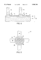
- FIG. 6 is a plan view illustrating a bundle of spacers over an adhesion site on a faceplate.
- frit a glass powder
- a compatible photoresist are mixed together to form a mixture.
- Conventional frits such as Corning 7572 or 7575
- known positive and negative photoresists such as OCG SC negative photoresists
- OCG SC negative photoresists can be used.
- a resist such as OCG SC100 or a polyvinyl alcohol (PVA) based resist
- the mixture is preferably about 1-5% by weight of frit and about 95-99% by weight of resist, and more preferably about 2% by weight of frit and about 98% by weight of resist.
- the resist and frit are mixed with a low shear technique until a substantially homogeneous mixture without bubbles or froth is obtained.
- the combination can be mixed for about 30-60 minutes.
- mixture 30 of frit and photoresist is applied with an even thickness to a faceplate 32 by using known techniques, such as spin coating or spraying.
- Faceplate 32 has a transparent dielectric layer 34, preferably glass, and a transparent conductive layer 36, such as tin oxide or indium tin oxide (ITO), coating dielectric layer 34.
- a transparent conductive layer 36 such as tin oxide or indium tin oxide (ITO), coating dielectric layer 34.
- Over conductive layer 36 is a patterned grille 38 made of an opaque, non-reflective material, such as cobalt oxide, manganese oxide, or diaqueous graphite (DAG). Grille 38 defines regions 40 where phosphor particles will later be coated.
- Mixture 30 thus covers grille 38 and regions 40 (which are not covered by grille 38).
- the assembly of faceplate 32 and mixture 30 is heated (softbaked) to cure the resist. If the mixture uses OCG SC negative resist, the substrate is heated to about 80-100° C. for
- the resist is then exposed and developed to create desired regions of the mixture of frit and cured photoresist that serve as adhesion sites 42. Exposure is performed according to known techniques, such as using an aligner to align a mask with the assembly and then exposing the masked assembly with known methods, such as projection lithography or contact printing. E-beam lithography could also be used. After exposure, the mixture is developed using an appropriate developing solvent, such as WNRD. The mixture can be developed with a dip-develop technique or a spray-develop technique. For the dip-develop technique, faceplate 32 with mixture 30 is immersed in developer for about two minutes with gentle agitation, and is then removed and put into a second tank with a rinse for about 30 seconds.
- the developing and rinse times can vary depending on the thickness of the mixture, the softbake process, and other parameters.
- the developing typically takes about 1.5 to 3 minutes, and the rinse lasts for about 30 seconds.
- sites 42 are formed at desired alternating intersections of rows and columns of grille 38.
- the sites could be formed at all intersections or at fewer intersections, or on portions of grille 38 between intersections.
- the number of adhesion sites with spacers will depend on the strength of the spacers and the size of the display.
- a glazing step may be performed to help the frit stick together, and to burn off organics in the mixture. This step is typically performed at about 400-450° C., but the temperature could be different depending on the frit used.
- spacers 46 are then attached to faceplate 32 with the frit serving as the adhesive.
- One way to attach spacers is to provide glass spacers in bundles with binder fibers as described in detail in U.S. Pat. No. 5,486,126, and in application Ser. No. 08/528,761, both of which are expressly incorporated herein by reference for all purposes.
- Large numbers of spacers 46 are formed in bundles 50 and clamped with uniform pressure to the faceplate at adhesion sites 42 at the intersection of rows and columns of grille 38. Bundles 50 and faceplate 32 are then heated sufficiently to soften the frit.
- spacers 46 in bundle 50 are firmly attached to grille 38 at sites 42, and thus extend perpendicularly away from the faceplate.
- the spacers can then be further processed, e.g., with a planarization technique, such as chemical-mechanical planarization (CMP).
- CMP chemical-mechanical planarization
- the faceplate with spacers is then assembled with the backplate/cathode in a vacuum-sealed package in a generally known manner to produce a display, such as a display similar in principle to that in FIG. 1.
- the spacers extend to and rest on the extraction grid of the cathode, but preferably are not held there with adhesive; rather, the pressure differential holds the spacers in place.
- the mixture can also be provided to a backplate, preferably after conductive layers, a silicon layer, an oxide, and a conductive grid layer are formed, and prior to etching to form the emitter cones.
- the resulting adhesion sites are preferably on the conductive extraction grid.
- the faceplate need not have a matrix grille, and if it does, spacers can be provided before or after the grille is formed. While a devitreous frit is preferred for the mixture, a vitreous frit can be used.
Abstract
Description
Claims (19)
Priority Applications (3)
| Application Number | Priority Date | Filing Date | Title |
|---|---|---|---|
| US08/764,485 US5984746A (en) | 1996-12-12 | 1996-12-12 | Attaching spacers in a display device |
| US09/438,936 US6491559B1 (en) | 1996-12-12 | 1999-11-12 | Attaching spacers in a display device |
| US10/315,599 US6696783B2 (en) | 1996-12-12 | 2002-12-10 | Attaching spacers in a display device on desired locations of a conductive layer |
Applications Claiming Priority (1)
| Application Number | Priority Date | Filing Date | Title |
|---|---|---|---|
| US08/764,485 US5984746A (en) | 1996-12-12 | 1996-12-12 | Attaching spacers in a display device |
Related Child Applications (1)
| Application Number | Title | Priority Date | Filing Date |
|---|---|---|---|
| US09/438,936 Continuation US6491559B1 (en) | 1996-12-12 | 1999-11-12 | Attaching spacers in a display device |
Publications (1)
| Publication Number | Publication Date |
|---|---|
| US5984746A true US5984746A (en) | 1999-11-16 |
Family
ID=25070866
Family Applications (3)
| Application Number | Title | Priority Date | Filing Date |
|---|---|---|---|
| US08/764,485 Expired - Fee Related US5984746A (en) | 1996-12-12 | 1996-12-12 | Attaching spacers in a display device |
| US09/438,936 Expired - Fee Related US6491559B1 (en) | 1996-12-12 | 1999-11-12 | Attaching spacers in a display device |
| US10/315,599 Expired - Fee Related US6696783B2 (en) | 1996-12-12 | 2002-12-10 | Attaching spacers in a display device on desired locations of a conductive layer |
Family Applications After (2)
| Application Number | Title | Priority Date | Filing Date |
|---|---|---|---|
| US09/438,936 Expired - Fee Related US6491559B1 (en) | 1996-12-12 | 1999-11-12 | Attaching spacers in a display device |
| US10/315,599 Expired - Fee Related US6696783B2 (en) | 1996-12-12 | 2002-12-10 | Attaching spacers in a display device on desired locations of a conductive layer |
Country Status (1)
| Country | Link |
|---|---|
| US (3) | US5984746A (en) |
Cited By (2)
| Publication number | Priority date | Publication date | Assignee | Title |
|---|---|---|---|---|
| KR100416761B1 (en) * | 2001-06-12 | 2004-01-31 | 삼성에스디아이 주식회사 | Forming method of spacer in flat panel display |
| WO2023130516A1 (en) * | 2022-01-10 | 2023-07-13 | 深圳市华星光电半导体显示技术有限公司 | Metal film, display device and manufacturing method therefor |
Families Citing this family (2)
| Publication number | Priority date | Publication date | Assignee | Title |
|---|---|---|---|---|
| JP2002157959A (en) * | 2000-09-08 | 2002-05-31 | Canon Inc | Method of manufacturing spacer and method of manufacturing image forming device using this spacer |
| US8089579B1 (en) * | 2009-08-27 | 2012-01-03 | Rockwell Collins, Inc. | System and method for providing a light control mechanism for a display |
Citations (2)
| Publication number | Priority date | Publication date | Assignee | Title |
|---|---|---|---|---|
| US4732838A (en) * | 1985-12-31 | 1988-03-22 | General Electric Company | Method of forming a patterned glass layer over the surface of a substrate |
| US5716251A (en) * | 1995-09-15 | 1998-02-10 | Micron Display Technology, Inc. | Sacrificial spacers for large area displays |
Family Cites Families (32)
| Publication number | Priority date | Publication date | Assignee | Title |
|---|---|---|---|---|
| NL6603797A (en) | 1965-03-24 | 1967-01-25 | ||
| US3990874A (en) | 1965-09-24 | 1976-11-09 | Ni-Tec, Inc. | Process of manufacturing a fiber bundle |
| US3979621A (en) | 1969-06-04 | 1976-09-07 | American Optical Corporation | Microchannel plates |
| GB1509487A (en) | 1976-01-08 | 1978-05-04 | Ibm | Gas panel display devices |
| US4183125A (en) | 1976-10-06 | 1980-01-15 | Zenith Radio Corporation | Method of making an insulator-support for luminescent display panels and the like |
| DE3036671A1 (en) | 1980-09-29 | 1982-05-13 | Siemens AG, 1000 Berlin und 8000 München | FLAT SCREEN, METHOD FOR ITS PRODUCTION AND USE |
| US4705205A (en) | 1983-06-30 | 1987-11-10 | Raychem Corporation | Chip carrier mounting device |
| FR2623013A1 (en) | 1987-11-06 | 1989-05-12 | Commissariat Energie Atomique | ELECTRO SOURCE WITH EMISSIVE MICROPOINT CATHODES AND FIELD EMISSION-INDUCED CATHODOLUMINESCENCE VISUALIZATION DEVICE USING THE SOURCE |
| US4923421A (en) | 1988-07-06 | 1990-05-08 | Innovative Display Development Partners | Method for providing polyimide spacers in a field emission panel display |
| JPH02165540A (en) | 1988-12-19 | 1990-06-26 | Narumi China Corp | Formation of plasma display panel barrier |
| FR2641412B1 (en) | 1988-12-30 | 1991-02-15 | Thomson Tubes Electroniques | FIELD EMISSION TYPE ELECTRON SOURCE |
| JP3035983B2 (en) | 1989-11-09 | 2000-04-24 | ソニー株式会社 | Manufacturing method of cathode ray tube |
| JPH03179630A (en) | 1989-12-07 | 1991-08-05 | Nec Corp | Manufacture of spacer of plasma display panel |
| US5136764A (en) | 1990-09-27 | 1992-08-11 | Motorola, Inc. | Method for forming a field emission device |
| NL9100122A (en) | 1991-01-25 | 1992-08-17 | Philips Nv | DISPLAY DEVICE. |
| US5229691A (en) | 1991-02-25 | 1993-07-20 | Panocorp Display Systems | Electronic fluorescent display |
| US5151061A (en) | 1992-02-21 | 1992-09-29 | Micron Technology, Inc. | Method to form self-aligned tips for flat panel displays |
| US5205770A (en) | 1992-03-12 | 1993-04-27 | Micron Technology, Inc. | Method to form high aspect ratio supports (spacers) for field emission display using micro-saw technology |
| US5449970A (en) | 1992-03-16 | 1995-09-12 | Microelectronics And Computer Technology Corporation | Diode structure flat panel display |
| US5232549A (en) | 1992-04-14 | 1993-08-03 | Micron Technology, Inc. | Spacers for field emission display fabricated via self-aligned high energy ablation |
| US5342737A (en) | 1992-04-27 | 1994-08-30 | The United States Of America As Represented By The Secretary Of The Navy | High aspect ratio metal microstructures and method for preparing the same |
| US5329207A (en) | 1992-05-13 | 1994-07-12 | Micron Technology, Inc. | Field emission structures produced on macro-grain polysilicon substrates |
| US5391259A (en) | 1992-05-15 | 1995-02-21 | Micron Technology, Inc. | Method for forming a substantially uniform array of sharp tips |
| US5374868A (en) | 1992-09-11 | 1994-12-20 | Micron Display Technology, Inc. | Method for formation of a trench accessible cold-cathode field emission device |
| US5347292A (en) | 1992-10-28 | 1994-09-13 | Panocorp Display Systems | Super high resolution cold cathode fluorescent display |
| US5686790A (en) * | 1993-06-22 | 1997-11-11 | Candescent Technologies Corporation | Flat panel device with ceramic backplate |
| US5342477A (en) | 1993-07-14 | 1994-08-30 | Micron Display Technology, Inc. | Low resistance electrodes useful in flat panel displays |
| US5445550A (en) | 1993-12-22 | 1995-08-29 | Xie; Chenggang | Lateral field emitter device and method of manufacturing same |
| US5448131A (en) | 1994-04-13 | 1995-09-05 | Texas Instruments Incorporated | Spacer for flat panel display |
| JP3305166B2 (en) | 1994-06-27 | 2002-07-22 | キヤノン株式会社 | Electron beam equipment |
| US5486126A (en) | 1994-11-18 | 1996-01-23 | Micron Display Technology, Inc. | Spacers for large area displays |
| US5730636A (en) * | 1995-09-29 | 1998-03-24 | Micron Display Technology, Inc. | Self-dimensioning support member for use in a field emission display |
-
1996
- 1996-12-12 US US08/764,485 patent/US5984746A/en not_active Expired - Fee Related
-
1999
- 1999-11-12 US US09/438,936 patent/US6491559B1/en not_active Expired - Fee Related
-
2002
- 2002-12-10 US US10/315,599 patent/US6696783B2/en not_active Expired - Fee Related
Patent Citations (2)
| Publication number | Priority date | Publication date | Assignee | Title |
|---|---|---|---|---|
| US4732838A (en) * | 1985-12-31 | 1988-03-22 | General Electric Company | Method of forming a patterned glass layer over the surface of a substrate |
| US5716251A (en) * | 1995-09-15 | 1998-02-10 | Micron Display Technology, Inc. | Sacrificial spacers for large area displays |
Cited By (2)
| Publication number | Priority date | Publication date | Assignee | Title |
|---|---|---|---|---|
| KR100416761B1 (en) * | 2001-06-12 | 2004-01-31 | 삼성에스디아이 주식회사 | Forming method of spacer in flat panel display |
| WO2023130516A1 (en) * | 2022-01-10 | 2023-07-13 | 深圳市华星光电半导体显示技术有限公司 | Metal film, display device and manufacturing method therefor |
Also Published As
| Publication number | Publication date |
|---|---|
| US6696783B2 (en) | 2004-02-24 |
| US20030080674A1 (en) | 2003-05-01 |
| US6491559B1 (en) | 2002-12-10 |
Similar Documents
| Publication | Publication Date | Title |
|---|---|---|
| US5486126A (en) | Spacers for large area displays | |
| US6329750B1 (en) | Anodically-bonded elements for flat panel displays | |
| US5705079A (en) | Method for forming spacers in flat panel displays using photo-etching | |
| US6458515B2 (en) | Structures, lithographic mask forming solutions, mask forming methods, field emission display emitter mask forming methods, and methods of forming plural field emission display emitters | |
| US6387600B1 (en) | Protective layer during lithography and etch | |
| US6413135B1 (en) | Spacer fabrication for flat panel displays | |
| US5962969A (en) | Sacrificial spacers for large area displays | |
| JP2001076652A (en) | Flat display device and its manufacture | |
| US5984746A (en) | Attaching spacers in a display device | |
| US6312302B1 (en) | Manufacturing method for a flat panel display and the display with reinforced support spacers | |
| US6560997B2 (en) | Method of making glass structures for flat panel displays | |
| US6255773B1 (en) | Field emission display having a cathodoluminescent anode | |
| WO1998040901A1 (en) | Method for forming spacers in flat panel displays using photo-etching | |
| KR100203956B1 (en) | Forming method of spacers for large area displays | |
| CN1261964C (en) | Field emission display and method of manufacture | |
| TW293135B (en) | Process of fabricating field emission display spacer | |
| KR20020094980A (en) | Forming method of spacer in flat panel display | |
| WO2006019033A1 (en) | Method for manufacturing image display and image display | |
| JPH09231919A (en) | Image display device using electric field emission cold cathode | |
| KR20070056603A (en) | Manufacturing method of electron emission device |
Legal Events
| Date | Code | Title | Description |
|---|---|---|---|
| AS | Assignment |
Owner name: MICRON DISPLAY TECHNOLOGY, INC., IDAHO Free format text: ASSIGNMENT OF ASSIGNORS INTEREST;ASSIGNORS:RASMUSSEN, ROBERT T.;CATHEY, DAVID A.;REEL/FRAME:008363/0193 Effective date: 19961210 |
|
| AS | Assignment |
Owner name: MICRON TECHNOLOGY, INC., IDAHO Free format text: MERGER;ASSIGNOR:MICRON DISPLAY TECHNOLOGY, INC.;REEL/FRAME:010217/0864 Effective date: 19970916 |
|
| FPAY | Fee payment |
Year of fee payment: 4 |
|
| FPAY | Fee payment |
Year of fee payment: 8 |
|
| REMI | Maintenance fee reminder mailed | ||
| LAPS | Lapse for failure to pay maintenance fees | ||
| STCH | Information on status: patent discontinuation |
Free format text: PATENT EXPIRED DUE TO NONPAYMENT OF MAINTENANCE FEES UNDER 37 CFR 1.362 |
|
| FP | Lapsed due to failure to pay maintenance fee |
Effective date: 20111116 |