US5998104A - Method of stripping a resist mask - Google Patents
Method of stripping a resist mask Download PDFInfo
- Publication number
- US5998104A US5998104A US08/972,251 US97225197A US5998104A US 5998104 A US5998104 A US 5998104A US 97225197 A US97225197 A US 97225197A US 5998104 A US5998104 A US 5998104A
- Authority
- US
- United States
- Prior art keywords
- ashing method
- downstream
- water vapor
- oxygen
- semiconductor wafer
- Prior art date
- Legal status (The legal status is an assumption and is not a legal conclusion. Google has not performed a legal analysis and makes no representation as to the accuracy of the status listed.)
- Expired - Fee Related
Links
Images


Classifications
-
- H—ELECTRICITY
- H01—ELECTRIC ELEMENTS
- H01L—SEMICONDUCTOR DEVICES NOT COVERED BY CLASS H10
- H01L21/00—Processes or apparatus adapted for the manufacture or treatment of semiconductor or solid state devices or of parts thereof
- H01L21/02—Manufacture or treatment of semiconductor devices or of parts thereof
- H01L21/04—Manufacture or treatment of semiconductor devices or of parts thereof the devices having at least one potential-jump barrier or surface barrier, e.g. PN junction, depletion layer or carrier concentration layer
- H01L21/18—Manufacture or treatment of semiconductor devices or of parts thereof the devices having at least one potential-jump barrier or surface barrier, e.g. PN junction, depletion layer or carrier concentration layer the devices having semiconductor bodies comprising elements of Group IV of the Periodic System or AIIIBV compounds with or without impurities, e.g. doping materials
- H01L21/30—Treatment of semiconductor bodies using processes or apparatus not provided for in groups H01L21/20 - H01L21/26
- H01L21/302—Treatment of semiconductor bodies using processes or apparatus not provided for in groups H01L21/20 - H01L21/26 to change their surface-physical characteristics or shape, e.g. etching, polishing, cutting
-
- G—PHYSICS
- G03—PHOTOGRAPHY; CINEMATOGRAPHY; ANALOGOUS TECHNIQUES USING WAVES OTHER THAN OPTICAL WAVES; ELECTROGRAPHY; HOLOGRAPHY
- G03F—PHOTOMECHANICAL PRODUCTION OF TEXTURED OR PATTERNED SURFACES, e.g. FOR PRINTING, FOR PROCESSING OF SEMICONDUCTOR DEVICES; MATERIALS THEREFOR; ORIGINALS THEREFOR; APPARATUS SPECIALLY ADAPTED THEREFOR
- G03F7/00—Photomechanical, e.g. photolithographic, production of textured or patterned surfaces, e.g. printing surfaces; Materials therefor, e.g. comprising photoresists; Apparatus specially adapted therefor
- G03F7/26—Processing photosensitive materials; Apparatus therefor
- G03F7/42—Stripping or agents therefor
- G03F7/427—Stripping or agents therefor using plasma means only
Definitions
- This invention is directed to a method of stripping a resist mask (referred to hereinafter as ashing).
- a mask made of an organic photoresist, etc. is necessarily employed in a photo-lithography technique for fabricating semiconductor devices. After the photoresist is exposed to light for the photo-lithography technique the resist must be removed.
- a dry plasma etching method particularly a downstream ashing method, is widely used for removing the used photo-resist.
- a downstream etching apparatus which can be employed is disclosed in U.S. Pat. No. 4,512,868 by the present inventor. This apparatus has been used for processing a silicon wafer, etc., where the wafer is protected from being bombarded by charged plasma particles.
- the reaction gas used for ashing the organic photo-resist is, for example, an oxygen gas including a CF 4 (carbon tetra-fluoride) gas.
- an oxygen gas including a CF 4 (carbon tetra-fluoride) gas is not always easy to remove the used resist. This is because the resist has been affected by its exposure to light during an exposure process and also its exposure to plasma during a prior silicon etching process, and therefore has become hardened.
- the CF 4 gas is apt to undesirably etch the silicon wafer.
- the ashing rate For improving the ashing rate, there is a method in which nitrogen gas is added to oxygen containing a reaction gas for increasing the number of oxygen atoms as a reaction species.
- the reaction gas contains 10% nitrogen
- the ashing rate is 0.3 ⁇ m/minute at 180° C.
- the increase of the ashing rate achieved with this method is still limited, however, because the reactive species are mainly only the oxygen atoms.
- the function of the added nitrogen gas is considered to increase only the number of oxygen atoms as the reactive species.
- Another method for increasing the number of oxygen atoms is by employing a known plasma etching method in which a small amount of water vapor is added to the oxygen plasma gas.
- a known plasma etching method in which a small amount of water vapor is added to the oxygen plasma gas.
- no extensive study or application of this method has been carried out.
- a downstream etching apparatus in which water vapor is added to an oxygen gas as a reaction gas.
- the amount of added water vapor is preferably more than 1 per cent of the total reaction gas with respect to the flow rate.
- the addition of water vapor into the oxygen gas increases the reactive species and accordingly the ashing rate at a wafer processing temperature as low as 150° C.
- the lowered ashing temperature prevents metal atoms from contaminating the semiconductor wafer.
- FIG. 1 is a graph of the effects of water on the activation energy added to various reaction gases
- FIG. 2 is a graph of the effects of water added to an oxygen gas with respect to the ashing rate and the amount of atomic oxygen in the oxygen plasma according to the present invention
- FIG. 3 is a graph of the effects of nitrogen added to an oxygen gas with respect to the ashing rate and the amount of atomic oxygen in prior art gas plasma;
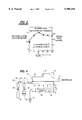
- FIG. 4 is a downstream ashing apparatus according to an embodiment of the present invention.
- FIG. 5 is an apparatus for mixing the water vapor into oxygen gas according to the embodiment of the present invention.
- FIG. 4 An apparatus used for obtaining the data in FIGS. 1 to 3 is schematically illustrated in FIG. 4.
- This apparatus is commonly used for downstream ashing, where microwaves, having a power of typically 2.45 GHz, are fed through a waveguide 1 into a microwave cavity 2.
- a plasma generating chamber 8 is a part of the cavity 2 and is vacuum-sealed by a quartz plate 2' which is transparent to the microwaves.
- Reaction gases of oxygen and water are fed from outside sources 37 and 38 through valves 35 and 36, and flow meters 33 and 34, respectively, to the plasma generating chamber 8. Accordingly, a plasma of the reaction gases is generated in the plasma generating chamber 8.
- a wall 4 opposite to the quartz plate 2', of the plasma generating chamber 8 many small holes 41 are provided which connect the plasma generating chamber 8 to a reaction chamber 5 but act as a shield to the microwaves.
- a reactive species such as oxygen atoms, generated in the plasma flows out of the plasma generating chamber 8 through the holes 41 into the relation chamber 5, as shown by arrows in FIG. 4.
- a semiconductor wafer 7 to be processed is placed on a stage 6 in the flow of the reaction gas from the holes 41.
- the reactive species reacts with the resist on the semiconductor wafer 7.
- the temperature of the stage 6 is raised and controlled by a heater 61 installed in the stage.
- the reaction gas in the reaction chamber 5 is evacuated by a pump through an outlet 51.
- the wafer 7 on the stage is heated to as high as approximately 200° C. while the chamber 5 is evacuated to approximately 0.01 Torr by the pump.
- the inner pressure of the reaction chamber 5 is raised to a pressure of approximately 0.8 Torr and approximately 1.5 kW of power (via microwaves) is applied to the plasma generating chamber 8 so as to generate a gas plasma therein.
- FIG. 1 is a graph of the effects on the activation energy of adding water, nitrogen or hydrogen to an oxygen gas, measured by their flow rate ratio.
- the activation energy is lowered from approximately 0.5 eV to approximately 0.4 eV by adding hydrogen or water; however, no effect is observed by adding nitrogen.
- a speed constant k of a chemical reaction is generally given by the following formula named Arrhenius' equation:
- A indicates a frequency factor
- E indicates an activation energy
- R indicates a gas constant
- T indicates absolute temperature. Therefore, a lowered value of the activation energy means a faster reaction at a certain temperature. That is, a certain reaction speed is achieved at a lower temperature.
- FIG. 2 The effects of adding water were observed by the inventors, and are shown in FIG. 2.
- the results in FIG. 2 were obtained by using the apparatus in FIG. 4 under the conditions of a reaction gas flow of 1,000 cc/min, including adding oxygen gas having water vapor and 50 sccm of argon gas.
- the wafer temperature is kept at 180° C.
- the percentage of the water vapor content, H 2 O/(O 2 +H 2 O) is measured by flow rate.
- the argon gas which has no effect on the ashing reaction, is added thereto just for generating a standard light spectrum with which oxygen atoms, etc., can be quantitatively compared using an actinometry technique, which is as reported by J. W.
- a glass fiber 9 is installed on the wall of the cavity 2 to measure the light generated in the plasma through the transparent quartz plate 2, which is also optically transparent. Another end of the glass fiber 9 is connected to a monochromator 10.
- black dots indicate an ashing rate scaled by the right hand side vertical axis
- white dots indicate the relative oxygen atom concentration scaled by the left hand side vertical axis.
- the relative oxygen atom concentration is measured by an actinometry method, i.e., by the ratio of the intensity of a 6158 ⁇ oxygen atom spectrum to the intensity of a 7067 ⁇ argon spectrum.
- FIG. 2 It can be seen in FIG. 2 that an addition of approximately 10% to 60% water vapor almost doubles the ashing rate compared to when no water is added.
- the ashing rate is completely related to the amount of the oxygen atom concentration.
- the ashing rate curve slowly falls but the oxygen atom concentration curve falls faster than the ashing rate curve.
- This separation of the oxygen atom concentration curve from the ashing rate curve suggests that another reactive species, such as an OH (hydroxide) radical, etc., is also contributing to the ashing reaction.
- FIG. 3 the effect of adding nitrogen to oxygen is shown in FIG. 3, for which the total gas flow and the temperature are the same as those in FIG. 2.
- the black and white dots represent the same thing as in FIG. 2, and the triangles represent a relative concentration of the oxygen atoms measured at a 4368 ⁇ oxygen atom spectrum.
- the ashing rates are almost the same, i.e., 0.3 ⁇ m/minutes, at 180° C.
- an ashing rate of 0.15 ⁇ m/minutes for 40% water-containing oxygen is achieved at as low as 150° C., compared with an ashing rate of 0.1 ⁇ m/minute for 10% nitrogen-containing oxygen which is optimum for the fastest ashing rate at the same temperature.
- a lowered temperature for the ashing process is significantly advantageous in that the semiconductor wafer is protected from contamination by the metal components in the resist material.
- metal contamination deteriorates the semiconductor properties, i.e., heavy metals lower the minority carrier generation lifetime, and alkaline metals contaminate the semiconductors.
- the curve of the ashing rate for water-containing oxygen is relatively flat over a wide range of water content, i.e., approximately 10% to 80%, and is much wider than the range of 5% to 15% for nitrogen-containing oxygen, as shown in FIG. 3. This is advantageous for easy control of an ashing operation during a production stage.
- the beneficial advantage of avoiding the use of CF 4 is as follows.
- 10% CF 4 -containing oxygen gas is used for resist etching in a downstream apparatus
- the SiO 2 layer on the semiconductor wafer is also undesirably etched.
- the ratio of the resist ashing rate to the SiO 2 etching rate, i.e., the selectivity, is typically 300 to 500. That is, while 1 ⁇ m of the resist is ashed, the SiO 2 is etched, for example, 30 ⁇ .
- This undesirable etching of the underlying SiO 2 layer used for a gate insulation lowers the withstand voltage of the gate insulation, or deteriorates the electrical characteristics of the semiconductor circuits.
- polycrystalline silicon, SiN, or aluminum as well.
- the gas plasma i.e., the electromagnetic power necessary for generating the plasma
- the gas plasma is confined in the plasma generating chamber by a shielding wall 4. Only the reactive species generated in the plasma comes out via the small holes 41 in the shielding wall 4.
- the holes shield the electromagnetic waves but allow the reactive species to pass therethrough to react with the resist material. Therefore, the wafer is protected from bombardment by the charged particles, such as ions, which may cause deterioration of the semiconductor materials. Therefore, the reaction is purely chemical.
- the above-described beneficial effects of adding water vapor to an oxygen gas can be significantly enhanced by also combining the beneficial effects of the downstream apparatus. Therefore, the apparatus is highly appreciated in the production of VLSI (very large scale integrated circuits) especially with respect to, for example, submicron integration.
- FIGS. 4 and 5 Preferred typical methods of adding water vapor to oxygen gas are schematically illustrated in FIGS. 4 and 5.
- the plasma generating chamber 8 is provided with two gas inlets 31 and 32 for introducing oxygen gas and water vapor respectively and independently from each other.
- Each gas is supplied to the inlet 31 and 32 from each gas source 37 and 38 through control valves 35 and 36 and flow meters 33 and 34, respectively.
- the amount of mixing necessary to mix the water vapor into the oxygen gas is influenced by the amount of oxygen gas flow and the fluid resistance of the inlet pipe where the inlet pipe connects to the plasma generating chamber 8.
- this problem can be solved.
- the water vapor is mixed into the oxygen while the oxygen gas is flowing. That is, the water vapor is bubbled through heated water 39 on the way from the gas source 37 to the plasma generating chamber 8.
- the amount of added water vapor is determined by the balance of the vapor pressure of the heated water 39 at its present temperature and the pressure of the oxygen.
- the water vapor pressure can be raised and controlled by the temperature of the water through which the oxygen gas is flowing.
- the water temperature is controlled by the heater 40. Because of the relatively high vapor pressure of the heated water, a considerable amount, such as more than 10%, of water vapor can be easily mixed with precision into the oxygen gas.
Abstract
A method for removing a used organic resist in a downstream ashing apparatus on a silicon semiconductor wafer in which water vapor is added to an oxygen plasma gas generated by microwaves. The addition of the water vapor lowers an activation energy of the ashing reaction and increases the reactive species generated in the plasma. Accordingly, the ashing rate is increased even at a wafer processing temperature as low as 150° C. The addition of water vapor increases the ashing rate for a wide range of the percentage of water content, such as 5 to 80%, allowing easy control of the process. The lowered operating temperature prevents contamination of the semiconductor wafer. Since CF4 is not used the SiO2 layer is protected from being undesirably etched and the semiconductor characteristics do not deteriorate.
Description
This application is a division of prior appliation Ser. No. 08/193,893, filed on Feb. 9, 1994 entitled METHOD OF STRIPPING A RESIST MASK, which is a continuation of prior application Ser. No. 08/069,402, filed Apr. 30, 1993, now abandoned, which is a continuation of application Ser. No. 07/590,595, filed Sep. 27, 1990, now abandoned, which is a continuation of prior application Ser. No. 07/232,096, filed Aug. 15, 1988, now abandoned.
This invention is directed to a method of stripping a resist mask (referred to hereinafter as ashing).
As is well known, a mask made of an organic photoresist, etc., is necessarily employed in a photo-lithography technique for fabricating semiconductor devices. After the photoresist is exposed to light for the photo-lithography technique the resist must be removed. A dry plasma etching method, particularly a downstream ashing method, is widely used for removing the used photo-resist. A downstream etching apparatus which can be employed is disclosed in U.S. Pat. No. 4,512,868 by the present inventor. This apparatus has been used for processing a silicon wafer, etc., where the wafer is protected from being bombarded by charged plasma particles.
The reaction gas used for ashing the organic photo-resist is, for example, an oxygen gas including a CF4 (carbon tetra-fluoride) gas. However, it is not always easy to remove the used resist. This is because the resist has been affected by its exposure to light during an exposure process and also its exposure to plasma during a prior silicon etching process, and therefore has become hardened. Furthermore, the CF4 gas is apt to undesirably etch the silicon wafer.
For improving the ashing rate, there is a method in which nitrogen gas is added to oxygen containing a reaction gas for increasing the number of oxygen atoms as a reaction species. In this method, for example, in which the reaction gas contains 10% nitrogen, the ashing rate is 0.3 μm/minute at 180° C. The increase of the ashing rate achieved with this method is still limited, however, because the reactive species are mainly only the oxygen atoms. The function of the added nitrogen gas is considered to increase only the number of oxygen atoms as the reactive species.
Another method for increasing the number of oxygen atoms is by employing a known plasma etching method in which a small amount of water vapor is added to the oxygen plasma gas. However, no extensive study or application of this method has been carried out.
It is an object of the present invention to provide an improved ashing method for quickly stripping a used resist on a semiconductor wafer.
It is another object of the present invention to lower the activation energy of the reaction, and accordingly lower the reaction temperature.
It is still another object of the present invention to prevent deterioration of the semiconductor wafer caused by contamination due to a metal component contained in the resist.
It is a further object of the present invention to avoid the use of CF4 gas so as to avoid an undesirable etching of a silicon wafer during the resist stripping, and accordingly prevent the lowering of the withstand voltage of an insulation layer.
According to the present invention a downstream etching apparatus is employed in which water vapor is added to an oxygen gas as a reaction gas. The amount of added water vapor is preferably more than 1 per cent of the total reaction gas with respect to the flow rate.
The addition of water vapor into the oxygen gas increases the reactive species and accordingly the ashing rate at a wafer processing temperature as low as 150° C. The lowered ashing temperature prevents metal atoms from contaminating the semiconductor wafer.
The above-mentioned features and advantages of the present invention, together with other objects and advantages which will become apparent, will be more fully described hereinafter, with reference being made to the accompanying drawings which form a part hereof, wherein like numerals refer to like parts throughout.
FIG. 1 is a graph of the effects of water on the activation energy added to various reaction gases;
FIG. 2 is a graph of the effects of water added to an oxygen gas with respect to the ashing rate and the amount of atomic oxygen in the oxygen plasma according to the present invention;
FIG. 3 is a graph of the effects of nitrogen added to an oxygen gas with respect to the ashing rate and the amount of atomic oxygen in prior art gas plasma;
FIG. 4 is a downstream ashing apparatus according to an embodiment of the present invention; and
FIG. 5 is an apparatus for mixing the water vapor into oxygen gas according to the embodiment of the present invention.
Referring to FIG. 1 through FIG. 3, the effects of the present invention are presented. An apparatus used for obtaining the data in FIGS. 1 to 3 is schematically illustrated in FIG. 4. This apparatus is commonly used for downstream ashing, where microwaves, having a power of typically 2.45 GHz, are fed through a waveguide 1 into a microwave cavity 2. A plasma generating chamber 8 is a part of the cavity 2 and is vacuum-sealed by a quartz plate 2' which is transparent to the microwaves. Reaction gases of oxygen and water are fed from outside sources 37 and 38 through valves 35 and 36, and flow meters 33 and 34, respectively, to the plasma generating chamber 8. Accordingly, a plasma of the reaction gases is generated in the plasma generating chamber 8. On a wall 4, opposite to the quartz plate 2', of the plasma generating chamber 8 many small holes 41 are provided which connect the plasma generating chamber 8 to a reaction chamber 5 but act as a shield to the microwaves. A reactive species, such as oxygen atoms, generated in the plasma flows out of the plasma generating chamber 8 through the holes 41 into the relation chamber 5, as shown by arrows in FIG. 4. In the reaction chamber 5, a semiconductor wafer 7 to be processed is placed on a stage 6 in the flow of the reaction gas from the holes 41. The reactive species reacts with the resist on the semiconductor wafer 7. The temperature of the stage 6 is raised and controlled by a heater 61 installed in the stage. The reaction gas in the reaction chamber 5 is evacuated by a pump through an outlet 51.
With respect to the ashing process, the wafer 7 on the stage is heated to as high as approximately 200° C. while the chamber 5 is evacuated to approximately 0.01 Torr by the pump. Next, the inner pressure of the reaction chamber 5 is raised to a pressure of approximately 0.8 Torr and approximately 1.5 kW of power (via microwaves) is applied to the plasma generating chamber 8 so as to generate a gas plasma therein.
FIG. 1 is a graph of the effects on the activation energy of adding water, nitrogen or hydrogen to an oxygen gas, measured by their flow rate ratio. In FIG. 1 it is shown that the activation energy is lowered from approximately 0.5 eV to approximately 0.4 eV by adding hydrogen or water; however, no effect is observed by adding nitrogen. On the other hand, as is well known, a speed constant k of a chemical reaction is generally given by the following formula named Arrhenius' equation:
k=A exp (-E/RT)
where A indicates a frequency factor, E indicates an activation energy, R indicates a gas constant and T indicates absolute temperature. Therefore, a lowered value of the activation energy means a faster reaction at a certain temperature. That is, a certain reaction speed is achieved at a lower temperature.
The effects of adding water were observed by the inventors, and are shown in FIG. 2. The results in FIG. 2 were obtained by using the apparatus in FIG. 4 under the conditions of a reaction gas flow of 1,000 cc/min, including adding oxygen gas having water vapor and 50 sccm of argon gas. The wafer temperature is kept at 180° C. The percentage of the water vapor content, H2 O/(O2 +H2 O), is measured by flow rate. The argon gas, which has no effect on the ashing reaction, is added thereto just for generating a standard light spectrum with which oxygen atoms, etc., can be quantitatively compared using an actinometry technique, which is as reported by J. W. Coburn et al., "Journal Applied Physics", Vol. 51, No. 6, pp. 3134 (1980). A glass fiber 9 is installed on the wall of the cavity 2 to measure the light generated in the plasma through the transparent quartz plate 2, which is also optically transparent. Another end of the glass fiber 9 is connected to a monochromator 10. In FIG. 2, black dots indicate an ashing rate scaled by the right hand side vertical axis, and white dots indicate the relative oxygen atom concentration scaled by the left hand side vertical axis. The relative oxygen atom concentration is measured by an actinometry method, i.e., by the ratio of the intensity of a 6158 Å oxygen atom spectrum to the intensity of a 7067 Å argon spectrum.
It can be seen in FIG. 2 that an addition of approximately 10% to 60% water vapor almost doubles the ashing rate compared to when no water is added. The ashing rate is completely related to the amount of the oxygen atom concentration. However, in a range of over 50% water content, the ashing rate curve slowly falls but the oxygen atom concentration curve falls faster than the ashing rate curve. This separation of the oxygen atom concentration curve from the ashing rate curve suggests that another reactive species, such as an OH (hydroxide) radical, etc., is also contributing to the ashing reaction. For comparison, the effect of adding nitrogen to oxygen is shown in FIG. 3, for which the total gas flow and the temperature are the same as those in FIG. 2.
In FIG. 3, the black and white dots, respectively, represent the same thing as in FIG. 2, and the triangles represent a relative concentration of the oxygen atoms measured at a 4368 Å oxygen atom spectrum. In FIG. 2 and FIG. 3, the ashing rates are almost the same, i.e., 0.3 μm/minutes, at 180° C. When the activation energy is lowered, however, an ashing rate of 0.15 μm/minutes for 40% water-containing oxygen is achieved at as low as 150° C., compared with an ashing rate of 0.1 μm/minute for 10% nitrogen-containing oxygen which is optimum for the fastest ashing rate at the same temperature. These data are not shown in the figures. A lowered temperature for the ashing process is significantly advantageous in that the semiconductor wafer is protected from contamination by the metal components in the resist material. As is well known, metal contamination deteriorates the semiconductor properties, i.e., heavy metals lower the minority carrier generation lifetime, and alkaline metals contaminate the semiconductors.
As seen in FIG. 2, the curve of the ashing rate for water-containing oxygen is relatively flat over a wide range of water content, i.e., approximately 10% to 80%, and is much wider than the range of 5% to 15% for nitrogen-containing oxygen, as shown in FIG. 3. This is advantageous for easy control of an ashing operation during a production stage.
The beneficial advantage of avoiding the use of CF4 is as follows. When 10% CF4 -containing oxygen gas is used for resist etching in a downstream apparatus, the SiO2 layer on the semiconductor wafer is also undesirably etched. The ratio of the resist ashing rate to the SiO2 etching rate, i.e., the selectivity, is typically 300 to 500. That is, while 1 μm of the resist is ashed, the SiO2 is etched, for example, 30 Å. This undesirable etching of the underlying SiO2 layer used for a gate insulation lowers the withstand voltage of the gate insulation, or deteriorates the electrical characteristics of the semiconductor circuits. The same problem exists with polycrystalline silicon, SiN, or aluminum, as well. This problem has not been so serious in fabricating conventional relatively low-density LSI (large scale integrated circuits) because the insulation layer is as thick as 1000 Å for a 16 K bit memory device. However, this problem is now becoming serious for fabricating the most up-to-date 1 M bit memory devices, because the insulation layer is as thin as 200 Å or less. According to the method of the present invention, there is no longer an undesirable etching problem of the SiO2 layer or any other layer.
As described above, in the downstream ashing apparatus, the gas plasma, i.e., the electromagnetic power necessary for generating the plasma, is confined in the plasma generating chamber by a shielding wall 4. Only the reactive species generated in the plasma comes out via the small holes 41 in the shielding wall 4. The holes shield the electromagnetic waves but allow the reactive species to pass therethrough to react with the resist material. Therefore, the wafer is protected from bombardment by the charged particles, such as ions, which may cause deterioration of the semiconductor materials. Therefore, the reaction is purely chemical. The above-described beneficial effects of adding water vapor to an oxygen gas can be significantly enhanced by also combining the beneficial effects of the downstream apparatus. Therefore, the apparatus is highly appreciated in the production of VLSI (very large scale integrated circuits) especially with respect to, for example, submicron integration.
Preferred typical methods of adding water vapor to oxygen gas are schematically illustrated in FIGS. 4 and 5. In FIG. 5, the same or equivalent parts are denoted by the same numbers as those in FIG. 4. In the apparatus of FIG. 4, the plasma generating chamber 8 is provided with two gas inlets 31 and 32 for introducing oxygen gas and water vapor respectively and independently from each other. Each gas is supplied to the inlet 31 and 32 from each gas source 37 and 38 through control valves 35 and 36 and flow meters 33 and 34, respectively. If the gases are to be fed into the plasma generating chamber 8 through a single inlet, the amount of mixing necessary to mix the water vapor into the oxygen gas is influenced by the amount of oxygen gas flow and the fluid resistance of the inlet pipe where the inlet pipe connects to the plasma generating chamber 8. In this apparatus, it is not easy to control a large amount of water vapor, for example, more than 10%, to be added to the oxygen gas because of the relatively high gas pressure of the oxygen gas caused by the fluid resistance of the inlet pipe. However, this problem can be solved.
In the apparatus of FIG. 5, the water vapor is mixed into the oxygen while the oxygen gas is flowing. That is, the water vapor is bubbled through heated water 39 on the way from the gas source 37 to the plasma generating chamber 8. The amount of added water vapor is determined by the balance of the vapor pressure of the heated water 39 at its present temperature and the pressure of the oxygen. The water vapor pressure can be raised and controlled by the temperature of the water through which the oxygen gas is flowing. The water temperature is controlled by the heater 40. Because of the relatively high vapor pressure of the heated water, a considerable amount, such as more than 10%, of water vapor can be easily mixed with precision into the oxygen gas.
In FIG. 1, the addition of a hydrogen gas into oxygen gas effectively lowers the activation energy. However, as is well known, a mixture of more than 3% hydrogen gas in oxygen gas will cause an explosion. Therefore, hydrogen gas cannot be industrially employed as a plasma reaction gas.
The many features and advantages of the invention are apparent from the detailed specification and thus, it is intended by the appended claims to cover all such features and advantages of the method which fall within the true spirit and scope of the invention. Further, since numerous modifications and changes may readily occur to those skilled in the art, it is not desired to limit the invention to the exact construction and operation shown and described, and accordingly, all suitable modifications and equivalents may be resorted to, falling within the scope of the invention.
Claims (45)
1. A downstream ashing method for removing organic resist from a semiconductor wafer, comprising the steps of:
placing the semiconductor wafer having the organic resist thereon in a reaction chamber;
generating gas plasma in a plasma generating chamber by subjecting a gas mixture containing oxygen and water vapor to electromagnetic power, said plasma gas including a reactive species and charged particles,
introducing only the reactive species from said plasma generating chamber to said reaction chamber while shielding the semiconductor wafer from said electromagnetic power and charged particles; and
removing said organic resist on the semiconductor wafer by an ashing reaction between said resist and said reactive species in said reaction chamber.
2. The downstream ashing method according to claim 1, wherein said ashing reaction includes a second reactive species including hydroxide radicals and oxygen atoms.
3. The downstream ashing method according to claim 2, herein said second reactive species is supplied by the water vapor.
4. The downstream ashing method according to claim 2, wherein said second reactive species determines an ashing rate of said organic resist on the semiconductor wafer.
5. The downstream ashing method according to claim 1, wherein removing of said organic resist on the semiconductor wafer is performed quicker than removing of same by an ashing reaction associated with only oxygen atoms while maintaining an ashing temperature constant.
6. The downstream ashing method according to claim 1, wherein removing of said organic resist on the semiconductor wafer is performed at a lower ashing temperature than removing of same by an ashing reaction associated with only oxygen atoms while maintaining an ashing rate constant.
7. The downstream ashing method according to claim 1, wherein said ashing reaction is a purely chemical reaction.
8. The downstream ashing method according to claim 1, wherein said oxygen and water vapor are introduced separately into said plasma generating chamber from respective outside sources.
9. The downstream ashing method according to claim 1, wherein the semiconductor wafer includes an insulating layer having a thickness of 20 nm or less underlying said organic resist.
10. The downstream ashing method according to claim 9, wherein said insulating layer is a gate insulating layer of a submicron device for a very large scale integrated circuit.
11. The downstream ashing method according to claim 1, wherein an amount of said water vapor is preferably more than 1% of said gas mixture with respect to a flow rate.
12. The downstream ashing method according to claim 1, wherein removing of said organic resist on the semiconductor wafer is performed in a range of said water vapor between approximately 10% and 80% with respect to an ashing rate.
13. The downstream ashing method according to claim 1, wherein said reaction chamber is connected to said plasma generating chamber by a shielding wall having a hole through which said reactive species is introduced into said reaction chamber.
14. The downstream ashing method according to claim 13, wherein said shielding wall prevents said electromagnetic power and said charged particles from penetrating into said reaction chamber.
15. The downstream ashing method according to claim 1, wherein in advance of said gas mixture being introduced into said plasma generating chamber, said reaction chamber is evacuated to approximately 0.01 Torr in pressure by a pump.
16. The downstream ashing method according to claim 13, wherein the semiconductor wafer is placed on a stage in said reaction chamber such that the semiconductor wafer is parallel to said shielding wall.
17. The downstream ashing method according to claim 1, wherein a constant downstream of said reactive species is generated by introducing said oxygen and water vapor into said plasma generating chamber while said reaction chamber is evacuated by a pump.
18. The downstream ashing method according to claim 1, wherein said reactive species is free from a radical having a halogen atom.
19. A downstream ashing method for removing organic resist from a material to be processed, comprising the steps of:
placing the material having the organic resist thereon in a reaction chamber;
generating gas plasma in a plasma generating chamber by subjecting a gas mixture containing oxygen and water vapor to electromagnetic power, said gas plasma including a reactive species; and
introducing said reactive species from said plasma generating chamber to said reaction chamber while shielding the material from said electromagnetic power,
wherein said organic resist on the semiconductor wafer is removed through at least one ashing reaction with said reactive species in said reaction chamber.
20. A downstream ashing method for removing an organic resist film from a semiconductor wafer, comprising the steps of:
disposing the semiconductor wafer having the organic resist film thereon in a reaction chamber;
generating a gas plasma in a plasma generating chamber by subjecting a gas mixture to electromagnetic power, said gas plasma including reactive species of oxygen and OH (hydroxide); and
introducing said reactive species of oxygen and OH (hydroxide) from said plasma generating chamber to said reaction chamber while shielding the semiconductor wafer from said electromagnetic power,
wherein said organic resist film on the semiconductor wafer is removed by an ashing reaction with said reactive species of oxygen and OH (hydroxide) in said reaction chamber.
21. A downstream ashing method for removing a used organic resist on a semiconductor wafer, comprising the steps of:
(a) generating a gas plasma of an oxygen gas containing a water vapor by applying an electromagnetic power to a plasma generating chamber; and
(b) introducing reactive species, generated in the gas plasma from the plasma generating chamber via holes, toward the semiconductor wafer to react with the used organic resist, the wall and holes in the plasma generating chamber essentially shielding the semiconductor wafer from the electromagnetic power,
wherein the water vapor content is more than 1% of the total gas with respect to flow rate.
22. A downstream ashing method for removing a used organic resist according to claim 21, wherein the electromagnetic power is microwave power.
23. A downstream ashing method for removing a used organic resist according to claim 22, wherein frequency of the microwave power is approximately 2.45 GHz.
24. A downstream ashing method for removing a used organic resist on a semiconductor wafer, said method comprising the steps of:
(a) feeding a reaction gas of oxygen and water from outside sources through valves, and flow meters, to a plasma generating chamber;
(b) generating a plasma of the reaction gas in the plasma generating chamber;
(c) processing a semiconductor wafer in a reaction chamber which receives a reactive species which flows out of the plasma generating chamber through holes in a wall of the plasma generating chamber; and
(d) reacting the reactive species with the resist on the semiconductor wafer.
25. A downstream ashing method according to claim 24, wherein the reaction chamber has a pressure of approximately 0.8 Torr.
26. A downstream ashing method according to claim 24, wherein the water vapor content is more than 1% of the total reaction gas with respect to flow rate.
27. A downstream ashing method according to claim 24, wherein the water is water vapor, further comprising the step of mixing the water vapor with the oxygen by bubbling the water vapor through heated water into the flowing oxygen gas.
28. A downstream ashing method according to claim 27, wherein more than 10% water vapor can be mixed with the oxygen gas.
29. A downstream ashing method for removing a used organic resist according to claim 1, wherein the electromagnetic power is microwave power.
30. A downstream ashing method for removing a used organic resist according to claim 29, wherein frequency of the microwave power is approximately 2.45 GHz.
31. A downstream ashing method according to claim 1, wherein the reaction chamber has a pressure of approximately 0.8 Torr.
32. A downstream ashing method according to claim 1, further comprising the step of mixing the water vapor with the oxygen by bubbling the water vapor through heated water into the oxygen.
33. A downstream ashing method according to claim 32, wherein more than 10% water vapor is mixed with the oxygen.
34. A downstream ashing method for removing a used organic resist according to claim 19, wherein an amount of said water vapor is more than 1% of said gas mixture with respect to a flow rate.
35. A downstream ashing method for removing a used organic resist according to claim 19, wherein the electromagnetic power is microwave power.
36. A downstream ashing method for removing a used organic resist according to claim 35, wherein frequency of the microwave power is approximately 2.45 GHz.
37. A downstream ashing method according to claim 19, wherein the reaction chamber has a pressure of approximately 0.8 Torr.
38. A downstream ashing method according to claim 19, further comprising the step of mixing the water vapor with the oxygen by bubbling the water vapor through heated water into the oxygen.
39. A downstream ashing method according to claim 38, wherein more than 10% water vapor is mixed with the oxygen.
40. A downstream ashing method for removing a used organic resist according to claim 20, wherein an amount of said water vapor is more than 1% of said gas mixture with respect to a flow rate.
41. A downstream ashing method for removing a used organic resist according to claim 20, wherein the electromagnetic power is microwave power.
42. A downstream ashing method for removing a used organic resist according to claim 41, wherein frequency of the microwave power is approximately 2.45 GHz.
43. A downstream ashing method according to claim 20, wherein the reaction chamber has a pressure of approximately 0.8 Torr.
44. A downstream ashing method according to claim 20, further comprising the step of mixing the water vapor with the oxygen by bubbling the water vapor through heated water into the oxygen.
45. A downstream ashing method according to claim 44, wherein more than 10% water vapor is mixed with the oxygen.
Priority Applications (1)
| Application Number | Priority Date | Filing Date | Title |
|---|---|---|---|
| US08/972,251 US5998104A (en) | 1987-08-19 | 1997-11-18 | Method of stripping a resist mask |
Applications Claiming Priority (7)
| Application Number | Priority Date | Filing Date | Title |
|---|---|---|---|
| JP62203985A JPH0777211B2 (en) | 1987-08-19 | 1987-08-19 | Ashing method |
| JP62-203985 | 1987-08-19 | ||
| US23209688A | 1988-08-15 | 1988-08-15 | |
| US59059590A | 1990-09-27 | 1990-09-27 | |
| US6940293A | 1993-04-30 | 1993-04-30 | |
| US08/193,893 US5773201A (en) | 1987-08-19 | 1994-02-09 | Method of stripping a resist mask |
| US08/972,251 US5998104A (en) | 1987-08-19 | 1997-11-18 | Method of stripping a resist mask |
Related Parent Applications (1)
| Application Number | Title | Priority Date | Filing Date |
|---|---|---|---|
| US08/193,893 Division US5773201A (en) | 1987-08-19 | 1994-02-09 | Method of stripping a resist mask |
Publications (1)
| Publication Number | Publication Date |
|---|---|
| US5998104A true US5998104A (en) | 1999-12-07 |
Family
ID=16482878
Family Applications (3)
| Application Number | Title | Priority Date | Filing Date |
|---|---|---|---|
| US08/193,893 Expired - Lifetime US5773201A (en) | 1987-08-19 | 1994-02-09 | Method of stripping a resist mask |
| US08/972,435 Expired - Fee Related US5961775A (en) | 1987-08-19 | 1997-11-18 | Apparatus for removing organic resist from semiconductor |
| US08/972,251 Expired - Fee Related US5998104A (en) | 1987-08-19 | 1997-11-18 | Method of stripping a resist mask |
Family Applications Before (2)
| Application Number | Title | Priority Date | Filing Date |
|---|---|---|---|
| US08/193,893 Expired - Lifetime US5773201A (en) | 1987-08-19 | 1994-02-09 | Method of stripping a resist mask |
| US08/972,435 Expired - Fee Related US5961775A (en) | 1987-08-19 | 1997-11-18 | Apparatus for removing organic resist from semiconductor |
Country Status (5)
| Country | Link |
|---|---|
| US (3) | US5773201A (en) |
| EP (1) | EP0304046B1 (en) |
| JP (1) | JPH0777211B2 (en) |
| KR (1) | KR910009319B1 (en) |
| DE (1) | DE3856395T2 (en) |
Cited By (4)
| Publication number | Priority date | Publication date | Assignee | Title |
|---|---|---|---|---|
| US6271115B1 (en) * | 2000-06-26 | 2001-08-07 | Chartered Semiconductor Manufacturing Ltd. | Post metal etch photoresist strip method |
| KR100685732B1 (en) * | 2001-06-05 | 2007-02-23 | 삼성전자주식회사 | Apparatus for removing a photoresist residue |
| US8779596B2 (en) | 2000-01-18 | 2014-07-15 | Micron Technology, Inc. | Structures and methods to enhance copper metallization |
| US8962469B2 (en) | 2012-02-16 | 2015-02-24 | Infineon Technologies Ag | Methods of stripping resist after metal deposition |
Families Citing this family (332)
| Publication number | Priority date | Publication date | Assignee | Title |
|---|---|---|---|---|
| JPH0777211B2 (en) * | 1987-08-19 | 1995-08-16 | 富士通株式会社 | Ashing method |
| US4961820A (en) * | 1988-06-09 | 1990-10-09 | Fujitsu Limited | Ashing method for removing an organic film on a substance of a semiconductor device under fabrication |
| JPH02263436A (en) * | 1989-04-03 | 1990-10-26 | Mitsubishi Electric Corp | Generating method of active chemical species and manufacture of electronic member material |
| DE69132811T2 (en) * | 1990-06-27 | 2002-04-04 | Fujitsu Ltd | METHOD FOR PRODUCING AN INTEGRATED SEMICONDUCTOR CIRCUIT |
| JP2510053B2 (en) * | 1990-06-27 | 1996-06-26 | 富士通株式会社 | Method of manufacturing semiconductor integrated circuit and manufacturing apparatus used therefor |
| US5545289A (en) * | 1994-02-03 | 1996-08-13 | Applied Materials, Inc. | Passivating, stripping and corrosion inhibition of semiconductor substrates |
| KR100336916B1 (en) * | 1994-02-03 | 2002-12-02 | 어플라이드 머티어리얼스, 인코포레이티드 | Stripping, passivation and corrosion inhibition methods for semiconductor substrates |
| US6228751B1 (en) * | 1995-09-08 | 2001-05-08 | Semiconductor Energy Laboratory Co., Ltd. | Method of manufacturing a semiconductor device |
| TW371796B (en) * | 1995-09-08 | 1999-10-11 | Semiconductor Energy Lab Co Ltd | Method and apparatus for manufacturing a semiconductor device |
| US6429120B1 (en) | 2000-01-18 | 2002-08-06 | Micron Technology, Inc. | Methods and apparatus for making integrated-circuit wiring from copper, silver, gold, and other metals |
| US20010012700A1 (en) * | 1998-12-15 | 2001-08-09 | Klaus F. Schuegraf | Semiconductor processing methods of chemical vapor depositing sio2 on a substrate |
| JP3193335B2 (en) * | 1997-12-12 | 2001-07-30 | 松下電器産業株式会社 | Method for manufacturing semiconductor device |
| US6105588A (en) | 1998-05-27 | 2000-08-22 | Micron Technology, Inc. | Method of resist stripping during semiconductor device fabrication |
| JPH11340127A (en) * | 1998-05-28 | 1999-12-10 | Nikon Corp | Etching method |
| US6207583B1 (en) * | 1998-09-04 | 2001-03-27 | Alliedsignal Inc. | Photoresist ashing process for organic and inorganic polymer dielectric materials |
| US6410417B1 (en) * | 1998-11-05 | 2002-06-25 | Promos Technologies, Inc. | Method of forming tungsten interconnect and vias without tungsten loss during wet stripping of photoresist polymer |
| US6372150B1 (en) * | 1998-12-18 | 2002-04-16 | Cypress Semiconductor Corp. | High vapor plasma strip methods and devices to enhance the reduction of organic residues over metal surfaces |
| US6307174B1 (en) * | 1999-02-01 | 2001-10-23 | United Microelectronics Corp. | Method for high-density plasma etching |
| US6281135B1 (en) | 1999-08-05 | 2001-08-28 | Axcelis Technologies, Inc. | Oxygen free plasma stripping process |
| US6492186B1 (en) | 1999-08-05 | 2002-12-10 | Eaton Corporation | Method for detecting an endpoint for an oxygen free plasma process |
| US6547458B1 (en) | 1999-11-24 | 2003-04-15 | Axcelis Technologies, Inc. | Optimized optical system design for endpoint detection |
| US6376370B1 (en) | 2000-01-18 | 2002-04-23 | Micron Technology, Inc. | Process for providing seed layers for using aluminum, copper, gold and silver metallurgy process for providing seed layers for using aluminum, copper, gold and silver metallurgy |
| US6667244B1 (en) | 2000-03-24 | 2003-12-23 | Gerald M. Cox | Method for etching sidewall polymer and other residues from the surface of semiconductor devices |
| US6440874B1 (en) * | 2000-03-24 | 2002-08-27 | Advanced Micro Devices, Inc. | High throughput plasma resist strip process for temperature sensitive applications |
| US6323121B1 (en) | 2000-05-12 | 2001-11-27 | Taiwan Semiconductor Manufacturing Company | Fully dry post-via-etch cleaning method for a damascene process |
| US6440864B1 (en) | 2000-06-30 | 2002-08-27 | Applied Materials Inc. | Substrate cleaning process |
| US6692903B2 (en) | 2000-12-13 | 2004-02-17 | Applied Materials, Inc | Substrate cleaning apparatus and method |
| US6834656B2 (en) * | 2001-05-23 | 2004-12-28 | Axcelis Technology, Inc. | Plasma process for removing polymer and residues from substrates |
| US6740594B2 (en) | 2001-05-31 | 2004-05-25 | Infineon Technologies Ag | Method for removing carbon-containing polysilane from a semiconductor without stripping |
| JP2003007689A (en) * | 2001-06-27 | 2003-01-10 | Seiko Epson Corp | Ashing apparatus/method, and method for manufacturing semiconductor device |
| US6991739B2 (en) * | 2001-10-15 | 2006-01-31 | Applied Materials, Inc. | Method of photoresist removal in the presence of a dielectric layer having a low k-value |
| US6713402B2 (en) * | 2002-05-31 | 2004-03-30 | Texas Instruments Incorporated | Methods for polymer removal following etch-stop layer etch |
| US6777173B2 (en) * | 2002-08-30 | 2004-08-17 | Lam Research Corporation | H2O vapor as a processing gas for crust, resist, and residue removal for post ion implant resist strip |
| US6926775B2 (en) | 2003-02-11 | 2005-08-09 | Micron Technology, Inc. | Reactors with isolated gas connectors and methods for depositing materials onto micro-device workpieces |
| US7581511B2 (en) * | 2003-10-10 | 2009-09-01 | Micron Technology, Inc. | Apparatus and methods for manufacturing microfeatures on workpieces using plasma vapor processes |
| US20050155690A1 (en) * | 2004-01-16 | 2005-07-21 | Park Edward H. | Bonding of dynamic vulcanizates of fluorocarbon elastomers |
| US7821655B2 (en) * | 2004-02-09 | 2010-10-26 | Axcelis Technologies, Inc. | In-situ absolute measurement process and apparatus for film thickness, film removal rate, and removal endpoint prediction |
| US7294736B2 (en) * | 2004-04-09 | 2007-11-13 | Cambrex Charles City, Inc. | Process for preparation of probucol derivatives |
| US8133554B2 (en) | 2004-05-06 | 2012-03-13 | Micron Technology, Inc. | Methods for depositing material onto microfeature workpieces in reaction chambers and systems for depositing materials onto microfeature workpieces |
| US7699932B2 (en) | 2004-06-02 | 2010-04-20 | Micron Technology, Inc. | Reactors, systems and methods for depositing thin films onto microfeature workpieces |
| US8193096B2 (en) | 2004-12-13 | 2012-06-05 | Novellus Systems, Inc. | High dose implantation strip (HDIS) in H2 base chemistry |
| US7387968B2 (en) * | 2005-11-08 | 2008-06-17 | Tokyo Electron Limited | Batch photoresist dry strip and ash system and process |
| KR100713707B1 (en) | 2006-05-04 | 2007-05-04 | 한국기계연구원 | Strip vapor system for photo resist of semiconductor wafer and method thereof |
| KR100814409B1 (en) * | 2006-08-14 | 2008-03-18 | 삼성전자주식회사 | Method of ashing an object and apparatus for performing the same |
| US8435895B2 (en) | 2007-04-04 | 2013-05-07 | Novellus Systems, Inc. | Methods for stripping photoresist and/or cleaning metal regions |
| US10378106B2 (en) | 2008-11-14 | 2019-08-13 | Asm Ip Holding B.V. | Method of forming insulation film by modified PEALD |
| US9394608B2 (en) | 2009-04-06 | 2016-07-19 | Asm America, Inc. | Semiconductor processing reactor and components thereof |
| US8802201B2 (en) * | 2009-08-14 | 2014-08-12 | Asm America, Inc. | Systems and methods for thin-film deposition of metal oxides using excited nitrogen-oxygen species |
| US20110143548A1 (en) | 2009-12-11 | 2011-06-16 | David Cheung | Ultra low silicon loss high dose implant strip |
| US9312155B2 (en) | 2011-06-06 | 2016-04-12 | Asm Japan K.K. | High-throughput semiconductor-processing apparatus equipped with multiple dual-chamber modules |
| US10364496B2 (en) | 2011-06-27 | 2019-07-30 | Asm Ip Holding B.V. | Dual section module having shared and unshared mass flow controllers |
| US10854498B2 (en) | 2011-07-15 | 2020-12-01 | Asm Ip Holding B.V. | Wafer-supporting device and method for producing same |
| US20130023129A1 (en) | 2011-07-20 | 2013-01-24 | Asm America, Inc. | Pressure transmitter for a semiconductor processing environment |
| US9613825B2 (en) | 2011-08-26 | 2017-04-04 | Novellus Systems, Inc. | Photoresist strip processes for improved device integrity |
| US9017481B1 (en) | 2011-10-28 | 2015-04-28 | Asm America, Inc. | Process feed management for semiconductor substrate processing |
| EP2604293A1 (en) * | 2011-12-14 | 2013-06-19 | Nederlandse Organisatie voor toegepast -natuurwetenschappelijk onderzoek TNO | A surface cleaning device and a method of cleaning a surface. |
| US9659799B2 (en) | 2012-08-28 | 2017-05-23 | Asm Ip Holding B.V. | Systems and methods for dynamic semiconductor process scheduling |
| US10714315B2 (en) | 2012-10-12 | 2020-07-14 | Asm Ip Holdings B.V. | Semiconductor reaction chamber showerhead |
| US9484191B2 (en) | 2013-03-08 | 2016-11-01 | Asm Ip Holding B.V. | Pulsed remote plasma method and system |
| US9589770B2 (en) | 2013-03-08 | 2017-03-07 | Asm Ip Holding B.V. | Method and systems for in-situ formation of intermediate reactive species |
| US9240412B2 (en) | 2013-09-27 | 2016-01-19 | Asm Ip Holding B.V. | Semiconductor structure and device and methods of forming same using selective epitaxial process |
| US10217627B2 (en) * | 2013-10-03 | 2019-02-26 | Applied Materials, Inc. | Methods of non-destructive post tungsten etch residue removal |
| US10683571B2 (en) | 2014-02-25 | 2020-06-16 | Asm Ip Holding B.V. | Gas supply manifold and method of supplying gases to chamber using same |
| US10167557B2 (en) | 2014-03-18 | 2019-01-01 | Asm Ip Holding B.V. | Gas distribution system, reactor including the system, and methods of using the same |
| US11015245B2 (en) | 2014-03-19 | 2021-05-25 | Asm Ip Holding B.V. | Gas-phase reactor and system having exhaust plenum and components thereof |
| US9514954B2 (en) | 2014-06-10 | 2016-12-06 | Lam Research Corporation | Peroxide-vapor treatment for enhancing photoresist-strip performance and modifying organic films |
| US10858737B2 (en) | 2014-07-28 | 2020-12-08 | Asm Ip Holding B.V. | Showerhead assembly and components thereof |
| US9890456B2 (en) | 2014-08-21 | 2018-02-13 | Asm Ip Holding B.V. | Method and system for in situ formation of gas-phase compounds |
| US10941490B2 (en) | 2014-10-07 | 2021-03-09 | Asm Ip Holding B.V. | Multiple temperature range susceptor, assembly, reactor and system including the susceptor, and methods of using the same |
| US9657845B2 (en) | 2014-10-07 | 2017-05-23 | Asm Ip Holding B.V. | Variable conductance gas distribution apparatus and method |
| KR102263121B1 (en) | 2014-12-22 | 2021-06-09 | 에이에스엠 아이피 홀딩 비.브이. | Semiconductor device and manufacuring method thereof |
| US10529542B2 (en) | 2015-03-11 | 2020-01-07 | Asm Ip Holdings B.V. | Cross-flow reactor and method |
| US10276355B2 (en) | 2015-03-12 | 2019-04-30 | Asm Ip Holding B.V. | Multi-zone reactor, system including the reactor, and method of using the same |
| US10458018B2 (en) | 2015-06-26 | 2019-10-29 | Asm Ip Holding B.V. | Structures including metal carbide material, devices including the structures, and methods of forming same |
| US10600673B2 (en) | 2015-07-07 | 2020-03-24 | Asm Ip Holding B.V. | Magnetic susceptor to baseplate seal |
| US9960072B2 (en) | 2015-09-29 | 2018-05-01 | Asm Ip Holding B.V. | Variable adjustment for precise matching of multiple chamber cavity housings |
| US10211308B2 (en) | 2015-10-21 | 2019-02-19 | Asm Ip Holding B.V. | NbMC layers |
| US10322384B2 (en) | 2015-11-09 | 2019-06-18 | Asm Ip Holding B.V. | Counter flow mixer for process chamber |
| US11139308B2 (en) | 2015-12-29 | 2021-10-05 | Asm Ip Holding B.V. | Atomic layer deposition of III-V compounds to form V-NAND devices |
| US10468251B2 (en) | 2016-02-19 | 2019-11-05 | Asm Ip Holding B.V. | Method for forming spacers using silicon nitride film for spacer-defined multiple patterning |
| US10529554B2 (en) | 2016-02-19 | 2020-01-07 | Asm Ip Holding B.V. | Method for forming silicon nitride film selectively on sidewalls or flat surfaces of trenches |
| US10501866B2 (en) | 2016-03-09 | 2019-12-10 | Asm Ip Holding B.V. | Gas distribution apparatus for improved film uniformity in an epitaxial system |
| US10343920B2 (en) | 2016-03-18 | 2019-07-09 | Asm Ip Holding B.V. | Aligned carbon nanotubes |
| US9892913B2 (en) | 2016-03-24 | 2018-02-13 | Asm Ip Holding B.V. | Radial and thickness control via biased multi-port injection settings |
| US10865475B2 (en) | 2016-04-21 | 2020-12-15 | Asm Ip Holding B.V. | Deposition of metal borides and silicides |
| US10190213B2 (en) | 2016-04-21 | 2019-01-29 | Asm Ip Holding B.V. | Deposition of metal borides |
| US10032628B2 (en) | 2016-05-02 | 2018-07-24 | Asm Ip Holding B.V. | Source/drain performance through conformal solid state doping |
| US10367080B2 (en) | 2016-05-02 | 2019-07-30 | Asm Ip Holding B.V. | Method of forming a germanium oxynitride film |
| KR102592471B1 (en) | 2016-05-17 | 2023-10-20 | 에이에스엠 아이피 홀딩 비.브이. | Method of forming metal interconnection and method of fabricating semiconductor device using the same |
| US11453943B2 (en) | 2016-05-25 | 2022-09-27 | Asm Ip Holding B.V. | Method for forming carbon-containing silicon/metal oxide or nitride film by ALD using silicon precursor and hydrocarbon precursor |
| US10388509B2 (en) | 2016-06-28 | 2019-08-20 | Asm Ip Holding B.V. | Formation of epitaxial layers via dislocation filtering |
| US10612137B2 (en) | 2016-07-08 | 2020-04-07 | Asm Ip Holdings B.V. | Organic reactants for atomic layer deposition |
| US9859151B1 (en) | 2016-07-08 | 2018-01-02 | Asm Ip Holding B.V. | Selective film deposition method to form air gaps |
| US10714385B2 (en) | 2016-07-19 | 2020-07-14 | Asm Ip Holding B.V. | Selective deposition of tungsten |
| US10381226B2 (en) | 2016-07-27 | 2019-08-13 | Asm Ip Holding B.V. | Method of processing substrate |
| US10395919B2 (en) | 2016-07-28 | 2019-08-27 | Asm Ip Holding B.V. | Method and apparatus for filling a gap |
| US9887082B1 (en) | 2016-07-28 | 2018-02-06 | Asm Ip Holding B.V. | Method and apparatus for filling a gap |
| US9812320B1 (en) | 2016-07-28 | 2017-11-07 | Asm Ip Holding B.V. | Method and apparatus for filling a gap |
| KR102532607B1 (en) | 2016-07-28 | 2023-05-15 | 에이에스엠 아이피 홀딩 비.브이. | Substrate processing apparatus and method of operating the same |
| KR102613349B1 (en) | 2016-08-25 | 2023-12-14 | 에이에스엠 아이피 홀딩 비.브이. | Exhaust apparatus and substrate processing apparatus and thin film fabricating method using the same |
| US10410943B2 (en) | 2016-10-13 | 2019-09-10 | Asm Ip Holding B.V. | Method for passivating a surface of a semiconductor and related systems |
| US10643826B2 (en) | 2016-10-26 | 2020-05-05 | Asm Ip Holdings B.V. | Methods for thermally calibrating reaction chambers |
| US11532757B2 (en) | 2016-10-27 | 2022-12-20 | Asm Ip Holding B.V. | Deposition of charge trapping layers |
| US10435790B2 (en) | 2016-11-01 | 2019-10-08 | Asm Ip Holding B.V. | Method of subatmospheric plasma-enhanced ALD using capacitively coupled electrodes with narrow gap |
| US10229833B2 (en) | 2016-11-01 | 2019-03-12 | Asm Ip Holding B.V. | Methods for forming a transition metal nitride film on a substrate by atomic layer deposition and related semiconductor device structures |
| US10714350B2 (en) | 2016-11-01 | 2020-07-14 | ASM IP Holdings, B.V. | Methods for forming a transition metal niobium nitride film on a substrate by atomic layer deposition and related semiconductor device structures |
| US10643904B2 (en) | 2016-11-01 | 2020-05-05 | Asm Ip Holdings B.V. | Methods for forming a semiconductor device and related semiconductor device structures |
| US10134757B2 (en) | 2016-11-07 | 2018-11-20 | Asm Ip Holding B.V. | Method of processing a substrate and a device manufactured by using the method |
| KR102546317B1 (en) | 2016-11-15 | 2023-06-21 | 에이에스엠 아이피 홀딩 비.브이. | Gas supply unit and substrate processing apparatus including the same |
| US10340135B2 (en) | 2016-11-28 | 2019-07-02 | Asm Ip Holding B.V. | Method of topologically restricted plasma-enhanced cyclic deposition of silicon or metal nitride |
| KR20180068582A (en) | 2016-12-14 | 2018-06-22 | 에이에스엠 아이피 홀딩 비.브이. | Substrate processing apparatus |
| US11447861B2 (en) | 2016-12-15 | 2022-09-20 | Asm Ip Holding B.V. | Sequential infiltration synthesis apparatus and a method of forming a patterned structure |
| US11581186B2 (en) | 2016-12-15 | 2023-02-14 | Asm Ip Holding B.V. | Sequential infiltration synthesis apparatus |
| KR20180070971A (en) | 2016-12-19 | 2018-06-27 | 에이에스엠 아이피 홀딩 비.브이. | Substrate processing apparatus |
| US10269558B2 (en) | 2016-12-22 | 2019-04-23 | Asm Ip Holding B.V. | Method of forming a structure on a substrate |
| US10867788B2 (en) | 2016-12-28 | 2020-12-15 | Asm Ip Holding B.V. | Method of forming a structure on a substrate |
| US10655221B2 (en) | 2017-02-09 | 2020-05-19 | Asm Ip Holding B.V. | Method for depositing oxide film by thermal ALD and PEALD |
| US10468261B2 (en) | 2017-02-15 | 2019-11-05 | Asm Ip Holding B.V. | Methods for forming a metallic film on a substrate by cyclical deposition and related semiconductor device structures |
| US10283353B2 (en) | 2017-03-29 | 2019-05-07 | Asm Ip Holding B.V. | Method of reforming insulating film deposited on substrate with recess pattern |
| US10529563B2 (en) | 2017-03-29 | 2020-01-07 | Asm Ip Holdings B.V. | Method for forming doped metal oxide films on a substrate by cyclical deposition and related semiconductor device structures |
| KR102457289B1 (en) | 2017-04-25 | 2022-10-21 | 에이에스엠 아이피 홀딩 비.브이. | Method for depositing a thin film and manufacturing a semiconductor device |
| US10892156B2 (en) | 2017-05-08 | 2021-01-12 | Asm Ip Holding B.V. | Methods for forming a silicon nitride film on a substrate and related semiconductor device structures |
| US10446393B2 (en) | 2017-05-08 | 2019-10-15 | Asm Ip Holding B.V. | Methods for forming silicon-containing epitaxial layers and related semiconductor device structures |
| US10770286B2 (en) | 2017-05-08 | 2020-09-08 | Asm Ip Holdings B.V. | Methods for selectively forming a silicon nitride film on a substrate and related semiconductor device structures |
| US10504742B2 (en) | 2017-05-31 | 2019-12-10 | Asm Ip Holding B.V. | Method of atomic layer etching using hydrogen plasma |
| US10886123B2 (en) | 2017-06-02 | 2021-01-05 | Asm Ip Holding B.V. | Methods for forming low temperature semiconductor layers and related semiconductor device structures |
| US11306395B2 (en) | 2017-06-28 | 2022-04-19 | Asm Ip Holding B.V. | Methods for depositing a transition metal nitride film on a substrate by atomic layer deposition and related deposition apparatus |
| US10685834B2 (en) | 2017-07-05 | 2020-06-16 | Asm Ip Holdings B.V. | Methods for forming a silicon germanium tin layer and related semiconductor device structures |
| KR20190009245A (en) | 2017-07-18 | 2019-01-28 | 에이에스엠 아이피 홀딩 비.브이. | Methods for forming a semiconductor device structure and related semiconductor device structures |
| US11374112B2 (en) | 2017-07-19 | 2022-06-28 | Asm Ip Holding B.V. | Method for depositing a group IV semiconductor and related semiconductor device structures |
| US11018002B2 (en) | 2017-07-19 | 2021-05-25 | Asm Ip Holding B.V. | Method for selectively depositing a Group IV semiconductor and related semiconductor device structures |
| US10541333B2 (en) | 2017-07-19 | 2020-01-21 | Asm Ip Holding B.V. | Method for depositing a group IV semiconductor and related semiconductor device structures |
| US10312055B2 (en) | 2017-07-26 | 2019-06-04 | Asm Ip Holding B.V. | Method of depositing film by PEALD using negative bias |
| US10590535B2 (en) | 2017-07-26 | 2020-03-17 | Asm Ip Holdings B.V. | Chemical treatment, deposition and/or infiltration apparatus and method for using the same |
| US10605530B2 (en) | 2017-07-26 | 2020-03-31 | Asm Ip Holding B.V. | Assembly of a liner and a flange for a vertical furnace as well as the liner and the vertical furnace |
| US10770336B2 (en) | 2017-08-08 | 2020-09-08 | Asm Ip Holding B.V. | Substrate lift mechanism and reactor including same |
| US10692741B2 (en) | 2017-08-08 | 2020-06-23 | Asm Ip Holdings B.V. | Radiation shield |
| US11139191B2 (en) | 2017-08-09 | 2021-10-05 | Asm Ip Holding B.V. | Storage apparatus for storing cassettes for substrates and processing apparatus equipped therewith |
| US10249524B2 (en) | 2017-08-09 | 2019-04-02 | Asm Ip Holding B.V. | Cassette holder assembly for a substrate cassette and holding member for use in such assembly |
| US11769682B2 (en) | 2017-08-09 | 2023-09-26 | Asm Ip Holding B.V. | Storage apparatus for storing cassettes for substrates and processing apparatus equipped therewith |
| USD900036S1 (en) | 2017-08-24 | 2020-10-27 | Asm Ip Holding B.V. | Heater electrical connector and adapter |
| US11830730B2 (en) | 2017-08-29 | 2023-11-28 | Asm Ip Holding B.V. | Layer forming method and apparatus |
| KR102491945B1 (en) | 2017-08-30 | 2023-01-26 | 에이에스엠 아이피 홀딩 비.브이. | Substrate processing apparatus |
| US11056344B2 (en) | 2017-08-30 | 2021-07-06 | Asm Ip Holding B.V. | Layer forming method |
| US11295980B2 (en) | 2017-08-30 | 2022-04-05 | Asm Ip Holding B.V. | Methods for depositing a molybdenum metal film over a dielectric surface of a substrate by a cyclical deposition process and related semiconductor device structures |
| US10607895B2 (en) | 2017-09-18 | 2020-03-31 | Asm Ip Holdings B.V. | Method for forming a semiconductor device structure comprising a gate fill metal |
| KR102630301B1 (en) | 2017-09-21 | 2024-01-29 | 에이에스엠 아이피 홀딩 비.브이. | Method of sequential infiltration synthesis treatment of infiltrateable material and structures and devices formed using same |
| US10844484B2 (en) | 2017-09-22 | 2020-11-24 | Asm Ip Holding B.V. | Apparatus for dispensing a vapor phase reactant to a reaction chamber and related methods |
| US10658205B2 (en) | 2017-09-28 | 2020-05-19 | Asm Ip Holdings B.V. | Chemical dispensing apparatus and methods for dispensing a chemical to a reaction chamber |
| US10403504B2 (en) | 2017-10-05 | 2019-09-03 | Asm Ip Holding B.V. | Method for selectively depositing a metallic film on a substrate |
| US10319588B2 (en) | 2017-10-10 | 2019-06-11 | Asm Ip Holding B.V. | Method for depositing a metal chalcogenide on a substrate by cyclical deposition |
| US10923344B2 (en) | 2017-10-30 | 2021-02-16 | Asm Ip Holding B.V. | Methods for forming a semiconductor structure and related semiconductor structures |
| KR102443047B1 (en) | 2017-11-16 | 2022-09-14 | 에이에스엠 아이피 홀딩 비.브이. | Method of processing a substrate and a device manufactured by the same |
| US10910262B2 (en) | 2017-11-16 | 2021-02-02 | Asm Ip Holding B.V. | Method of selectively depositing a capping layer structure on a semiconductor device structure |
| US11022879B2 (en) | 2017-11-24 | 2021-06-01 | Asm Ip Holding B.V. | Method of forming an enhanced unexposed photoresist layer |
| JP7214724B2 (en) | 2017-11-27 | 2023-01-30 | エーエスエム アイピー ホールディング ビー.ブイ. | Storage device for storing wafer cassettes used in batch furnaces |
| TWI791689B (en) | 2017-11-27 | 2023-02-11 | 荷蘭商Asm智慧財產控股私人有限公司 | Apparatus including a clean mini environment |
| US10290508B1 (en) | 2017-12-05 | 2019-05-14 | Asm Ip Holding B.V. | Method for forming vertical spacers for spacer-defined patterning |
| US10872771B2 (en) | 2018-01-16 | 2020-12-22 | Asm Ip Holding B. V. | Method for depositing a material film on a substrate within a reaction chamber by a cyclical deposition process and related device structures |
| TWI799494B (en) | 2018-01-19 | 2023-04-21 | 荷蘭商Asm 智慧財產控股公司 | Deposition method |
| WO2019142055A2 (en) | 2018-01-19 | 2019-07-25 | Asm Ip Holding B.V. | Method for depositing a gap-fill layer by plasma-assisted deposition |
| USD903477S1 (en) | 2018-01-24 | 2020-12-01 | Asm Ip Holdings B.V. | Metal clamp |
| US11018047B2 (en) | 2018-01-25 | 2021-05-25 | Asm Ip Holding B.V. | Hybrid lift pin |
| USD880437S1 (en) | 2018-02-01 | 2020-04-07 | Asm Ip Holding B.V. | Gas supply plate for semiconductor manufacturing apparatus |
| US10535516B2 (en) | 2018-02-01 | 2020-01-14 | Asm Ip Holdings B.V. | Method for depositing a semiconductor structure on a surface of a substrate and related semiconductor structures |
| US11081345B2 (en) | 2018-02-06 | 2021-08-03 | Asm Ip Holding B.V. | Method of post-deposition treatment for silicon oxide film |
| US10896820B2 (en) | 2018-02-14 | 2021-01-19 | Asm Ip Holding B.V. | Method for depositing a ruthenium-containing film on a substrate by a cyclical deposition process |
| US11685991B2 (en) | 2018-02-14 | 2023-06-27 | Asm Ip Holding B.V. | Method for depositing a ruthenium-containing film on a substrate by a cyclical deposition process |
| US10731249B2 (en) | 2018-02-15 | 2020-08-04 | Asm Ip Holding B.V. | Method of forming a transition metal containing film on a substrate by a cyclical deposition process, a method for supplying a transition metal halide compound to a reaction chamber, and related vapor deposition apparatus |
| US10658181B2 (en) | 2018-02-20 | 2020-05-19 | Asm Ip Holding B.V. | Method of spacer-defined direct patterning in semiconductor fabrication |
| KR102636427B1 (en) | 2018-02-20 | 2024-02-13 | 에이에스엠 아이피 홀딩 비.브이. | Substrate processing method and apparatus |
| US10975470B2 (en) | 2018-02-23 | 2021-04-13 | Asm Ip Holding B.V. | Apparatus for detecting or monitoring for a chemical precursor in a high temperature environment |
| US11473195B2 (en) | 2018-03-01 | 2022-10-18 | Asm Ip Holding B.V. | Semiconductor processing apparatus and a method for processing a substrate |
| US11629406B2 (en) | 2018-03-09 | 2023-04-18 | Asm Ip Holding B.V. | Semiconductor processing apparatus comprising one or more pyrometers for measuring a temperature of a substrate during transfer of the substrate |
| US11114283B2 (en) | 2018-03-16 | 2021-09-07 | Asm Ip Holding B.V. | Reactor, system including the reactor, and methods of manufacturing and using same |
| KR102646467B1 (en) | 2018-03-27 | 2024-03-11 | 에이에스엠 아이피 홀딩 비.브이. | Method of forming an electrode on a substrate and a semiconductor device structure including an electrode |
| US10510536B2 (en) | 2018-03-29 | 2019-12-17 | Asm Ip Holding B.V. | Method of depositing a co-doped polysilicon film on a surface of a substrate within a reaction chamber |
| US11230766B2 (en) | 2018-03-29 | 2022-01-25 | Asm Ip Holding B.V. | Substrate processing apparatus and method |
| US11088002B2 (en) | 2018-03-29 | 2021-08-10 | Asm Ip Holding B.V. | Substrate rack and a substrate processing system and method |
| KR102501472B1 (en) | 2018-03-30 | 2023-02-20 | 에이에스엠 아이피 홀딩 비.브이. | Substrate processing method |
| TWI811348B (en) | 2018-05-08 | 2023-08-11 | 荷蘭商Asm 智慧財產控股公司 | Methods for depositing an oxide film on a substrate by a cyclical deposition process and related device structures |
| KR20190129718A (en) | 2018-05-11 | 2019-11-20 | 에이에스엠 아이피 홀딩 비.브이. | Methods for forming a doped metal carbide film on a substrate and related semiconductor device structures |
| KR102596988B1 (en) | 2018-05-28 | 2023-10-31 | 에이에스엠 아이피 홀딩 비.브이. | Method of processing a substrate and a device manufactured by the same |
| TW202013553A (en) | 2018-06-04 | 2020-04-01 | 荷蘭商Asm 智慧財產控股公司 | Wafer handling chamber with moisture reduction |
| US11718913B2 (en) | 2018-06-04 | 2023-08-08 | Asm Ip Holding B.V. | Gas distribution system and reactor system including same |
| US11286562B2 (en) | 2018-06-08 | 2022-03-29 | Asm Ip Holding B.V. | Gas-phase chemical reactor and method of using same |
| US10797133B2 (en) | 2018-06-21 | 2020-10-06 | Asm Ip Holding B.V. | Method for depositing a phosphorus doped silicon arsenide film and related semiconductor device structures |
| KR102568797B1 (en) | 2018-06-21 | 2023-08-21 | 에이에스엠 아이피 홀딩 비.브이. | Substrate processing system |
| CN112292478A (en) | 2018-06-27 | 2021-01-29 | Asm Ip私人控股有限公司 | Cyclic deposition methods for forming metal-containing materials and films and structures containing metal-containing materials |
| JP2021529880A (en) | 2018-06-27 | 2021-11-04 | エーエスエム・アイピー・ホールディング・ベー・フェー | Periodic deposition methods for forming metal-containing materials and films and structures containing metal-containing materials |
| KR20200002519A (en) | 2018-06-29 | 2020-01-08 | 에이에스엠 아이피 홀딩 비.브이. | Method for depositing a thin film and manufacturing a semiconductor device |
| US10612136B2 (en) | 2018-06-29 | 2020-04-07 | ASM IP Holding, B.V. | Temperature-controlled flange and reactor system including same |
| US10755922B2 (en) | 2018-07-03 | 2020-08-25 | Asm Ip Holding B.V. | Method for depositing silicon-free carbon-containing film as gap-fill layer by pulse plasma-assisted deposition |
| US10388513B1 (en) | 2018-07-03 | 2019-08-20 | Asm Ip Holding B.V. | Method for depositing silicon-free carbon-containing film as gap-fill layer by pulse plasma-assisted deposition |
| US10767789B2 (en) | 2018-07-16 | 2020-09-08 | Asm Ip Holding B.V. | Diaphragm valves, valve components, and methods for forming valve components |
| US10483099B1 (en) | 2018-07-26 | 2019-11-19 | Asm Ip Holding B.V. | Method for forming thermally stable organosilicon polymer film |
| US11053591B2 (en) | 2018-08-06 | 2021-07-06 | Asm Ip Holding B.V. | Multi-port gas injection system and reactor system including same |
| US10883175B2 (en) | 2018-08-09 | 2021-01-05 | Asm Ip Holding B.V. | Vertical furnace for processing substrates and a liner for use therein |
| US10829852B2 (en) | 2018-08-16 | 2020-11-10 | Asm Ip Holding B.V. | Gas distribution device for a wafer processing apparatus |
| US11430674B2 (en) | 2018-08-22 | 2022-08-30 | Asm Ip Holding B.V. | Sensor array, apparatus for dispensing a vapor phase reactant to a reaction chamber and related methods |
| US11024523B2 (en) | 2018-09-11 | 2021-06-01 | Asm Ip Holding B.V. | Substrate processing apparatus and method |
| KR20200030162A (en) | 2018-09-11 | 2020-03-20 | 에이에스엠 아이피 홀딩 비.브이. | Method for deposition of a thin film |
| US11049751B2 (en) | 2018-09-14 | 2021-06-29 | Asm Ip Holding B.V. | Cassette supply system to store and handle cassettes and processing apparatus equipped therewith |
| CN110970344A (en) | 2018-10-01 | 2020-04-07 | Asm Ip控股有限公司 | Substrate holding apparatus, system including the same, and method of using the same |
| US11232963B2 (en) | 2018-10-03 | 2022-01-25 | Asm Ip Holding B.V. | Substrate processing apparatus and method |
| KR102592699B1 (en) | 2018-10-08 | 2023-10-23 | 에이에스엠 아이피 홀딩 비.브이. | Substrate support unit and apparatuses for depositing thin film and processing the substrate including the same |
| US10847365B2 (en) | 2018-10-11 | 2020-11-24 | Asm Ip Holding B.V. | Method of forming conformal silicon carbide film by cyclic CVD |
| US10811256B2 (en) | 2018-10-16 | 2020-10-20 | Asm Ip Holding B.V. | Method for etching a carbon-containing feature |
| KR102546322B1 (en) | 2018-10-19 | 2023-06-21 | 에이에스엠 아이피 홀딩 비.브이. | Substrate processing apparatus and substrate processing method |
| KR102605121B1 (en) | 2018-10-19 | 2023-11-23 | 에이에스엠 아이피 홀딩 비.브이. | Substrate processing apparatus and substrate processing method |
| USD948463S1 (en) | 2018-10-24 | 2022-04-12 | Asm Ip Holding B.V. | Susceptor for semiconductor substrate supporting apparatus |
| US10381219B1 (en) | 2018-10-25 | 2019-08-13 | Asm Ip Holding B.V. | Methods for forming a silicon nitride film |
| US11087997B2 (en) | 2018-10-31 | 2021-08-10 | Asm Ip Holding B.V. | Substrate processing apparatus for processing substrates |
| KR20200051105A (en) | 2018-11-02 | 2020-05-13 | 에이에스엠 아이피 홀딩 비.브이. | Substrate support unit and substrate processing apparatus including the same |
| US11572620B2 (en) | 2018-11-06 | 2023-02-07 | Asm Ip Holding B.V. | Methods for selectively depositing an amorphous silicon film on a substrate |
| US11031242B2 (en) | 2018-11-07 | 2021-06-08 | Asm Ip Holding B.V. | Methods for depositing a boron doped silicon germanium film |
| US10818758B2 (en) | 2018-11-16 | 2020-10-27 | Asm Ip Holding B.V. | Methods for forming a metal silicate film on a substrate in a reaction chamber and related semiconductor device structures |
| US10847366B2 (en) | 2018-11-16 | 2020-11-24 | Asm Ip Holding B.V. | Methods for depositing a transition metal chalcogenide film on a substrate by a cyclical deposition process |
| US10559458B1 (en) | 2018-11-26 | 2020-02-11 | Asm Ip Holding B.V. | Method of forming oxynitride film |
| US11217444B2 (en) | 2018-11-30 | 2022-01-04 | Asm Ip Holding B.V. | Method for forming an ultraviolet radiation responsive metal oxide-containing film |
| KR102636428B1 (en) | 2018-12-04 | 2024-02-13 | 에이에스엠 아이피 홀딩 비.브이. | A method for cleaning a substrate processing apparatus |
| US11158513B2 (en) | 2018-12-13 | 2021-10-26 | Asm Ip Holding B.V. | Methods for forming a rhenium-containing film on a substrate by a cyclical deposition process and related semiconductor device structures |
| TW202037745A (en) | 2018-12-14 | 2020-10-16 | 荷蘭商Asm Ip私人控股有限公司 | Method of forming device structure, structure formed by the method and system for performing the method |
| TWI819180B (en) | 2019-01-17 | 2023-10-21 | 荷蘭商Asm 智慧財產控股公司 | Methods of forming a transition metal containing film on a substrate by a cyclical deposition process |
| KR20200091543A (en) | 2019-01-22 | 2020-07-31 | 에이에스엠 아이피 홀딩 비.브이. | Semiconductor processing device |
| CN111524788B (en) | 2019-02-01 | 2023-11-24 | Asm Ip私人控股有限公司 | Method for topologically selective film formation of silicon oxide |
| KR20200102357A (en) | 2019-02-20 | 2020-08-31 | 에이에스엠 아이피 홀딩 비.브이. | Apparatus and methods for plug fill deposition in 3-d nand applications |
| JP2020136677A (en) | 2019-02-20 | 2020-08-31 | エーエスエム・アイピー・ホールディング・ベー・フェー | Periodic accumulation method for filing concave part formed inside front surface of base material, and device |
| KR102626263B1 (en) | 2019-02-20 | 2024-01-16 | 에이에스엠 아이피 홀딩 비.브이. | Cyclical deposition method including treatment step and apparatus for same |
| JP2020136678A (en) | 2019-02-20 | 2020-08-31 | エーエスエム・アイピー・ホールディング・ベー・フェー | Method for filing concave part formed inside front surface of base material, and device |
| TW202100794A (en) | 2019-02-22 | 2021-01-01 | 荷蘭商Asm Ip私人控股有限公司 | Substrate processing apparatus and method for processing substrate |
| KR20200108242A (en) | 2019-03-08 | 2020-09-17 | 에이에스엠 아이피 홀딩 비.브이. | Method for Selective Deposition of Silicon Nitride Layer and Structure Including Selectively-Deposited Silicon Nitride Layer |
| KR20200108243A (en) | 2019-03-08 | 2020-09-17 | 에이에스엠 아이피 홀딩 비.브이. | Structure Including SiOC Layer and Method of Forming Same |
| US11742198B2 (en) | 2019-03-08 | 2023-08-29 | Asm Ip Holding B.V. | Structure including SiOCN layer and method of forming same |
| JP2020167398A (en) | 2019-03-28 | 2020-10-08 | エーエスエム・アイピー・ホールディング・ベー・フェー | Door opener and substrate processing apparatus provided therewith |
| KR20200116855A (en) | 2019-04-01 | 2020-10-13 | 에이에스엠 아이피 홀딩 비.브이. | Method of manufacturing semiconductor device |
| US11447864B2 (en) | 2019-04-19 | 2022-09-20 | Asm Ip Holding B.V. | Layer forming method and apparatus |
| KR20200125453A (en) | 2019-04-24 | 2020-11-04 | 에이에스엠 아이피 홀딩 비.브이. | Gas-phase reactor system and method of using same |
| KR20200130121A (en) | 2019-05-07 | 2020-11-18 | 에이에스엠 아이피 홀딩 비.브이. | Chemical source vessel with dip tube |
| KR20200130118A (en) | 2019-05-07 | 2020-11-18 | 에이에스엠 아이피 홀딩 비.브이. | Method for Reforming Amorphous Carbon Polymer Film |
| KR20200130652A (en) | 2019-05-10 | 2020-11-19 | 에이에스엠 아이피 홀딩 비.브이. | Method of depositing material onto a surface and structure formed according to the method |
| JP2020188255A (en) | 2019-05-16 | 2020-11-19 | エーエスエム アイピー ホールディング ビー.ブイ. | Wafer boat handling device, vertical batch furnace, and method |
| USD975665S1 (en) | 2019-05-17 | 2023-01-17 | Asm Ip Holding B.V. | Susceptor shaft |
| USD947913S1 (en) | 2019-05-17 | 2022-04-05 | Asm Ip Holding B.V. | Susceptor shaft |
| USD935572S1 (en) | 2019-05-24 | 2021-11-09 | Asm Ip Holding B.V. | Gas channel plate |
| USD922229S1 (en) | 2019-06-05 | 2021-06-15 | Asm Ip Holding B.V. | Device for controlling a temperature of a gas supply unit |
| KR20200141003A (en) | 2019-06-06 | 2020-12-17 | 에이에스엠 아이피 홀딩 비.브이. | Gas-phase reactor system including a gas detector |
| KR20200143254A (en) | 2019-06-11 | 2020-12-23 | 에이에스엠 아이피 홀딩 비.브이. | Method of forming an electronic structure using an reforming gas, system for performing the method, and structure formed using the method |
| USD944946S1 (en) | 2019-06-14 | 2022-03-01 | Asm Ip Holding B.V. | Shower plate |
| USD931978S1 (en) | 2019-06-27 | 2021-09-28 | Asm Ip Holding B.V. | Showerhead vacuum transport |
| KR20210005515A (en) | 2019-07-03 | 2021-01-14 | 에이에스엠 아이피 홀딩 비.브이. | Temperature control assembly for substrate processing apparatus and method of using same |
| JP2021015791A (en) | 2019-07-09 | 2021-02-12 | エーエスエム アイピー ホールディング ビー.ブイ. | Plasma device and substrate processing method using coaxial waveguide |
| CN112216646A (en) | 2019-07-10 | 2021-01-12 | Asm Ip私人控股有限公司 | Substrate supporting assembly and substrate processing device comprising same |
| KR20210010307A (en) | 2019-07-16 | 2021-01-27 | 에이에스엠 아이피 홀딩 비.브이. | Substrate processing apparatus |
| KR20210010820A (en) | 2019-07-17 | 2021-01-28 | 에이에스엠 아이피 홀딩 비.브이. | Methods of forming silicon germanium structures |
| KR20210010816A (en) | 2019-07-17 | 2021-01-28 | 에이에스엠 아이피 홀딩 비.브이. | Radical assist ignition plasma system and method |
| US11643724B2 (en) | 2019-07-18 | 2023-05-09 | Asm Ip Holding B.V. | Method of forming structures using a neutral beam |
| TW202121506A (en) | 2019-07-19 | 2021-06-01 | 荷蘭商Asm Ip私人控股有限公司 | Method of forming topology-controlled amorphous carbon polymer film |
| TW202113936A (en) | 2019-07-29 | 2021-04-01 | 荷蘭商Asm Ip私人控股有限公司 | Methods for selective deposition utilizing n-type dopants and/or alternative dopants to achieve high dopant incorporation |
| CN112309899A (en) | 2019-07-30 | 2021-02-02 | Asm Ip私人控股有限公司 | Substrate processing apparatus |
| CN112309900A (en) | 2019-07-30 | 2021-02-02 | Asm Ip私人控股有限公司 | Substrate processing apparatus |
| US11587814B2 (en) | 2019-07-31 | 2023-02-21 | Asm Ip Holding B.V. | Vertical batch furnace assembly |
| US11587815B2 (en) | 2019-07-31 | 2023-02-21 | Asm Ip Holding B.V. | Vertical batch furnace assembly |
| US11227782B2 (en) | 2019-07-31 | 2022-01-18 | Asm Ip Holding B.V. | Vertical batch furnace assembly |
| CN112323048B (en) | 2019-08-05 | 2024-02-09 | Asm Ip私人控股有限公司 | Liquid level sensor for chemical source container |
| USD965524S1 (en) | 2019-08-19 | 2022-10-04 | Asm Ip Holding B.V. | Susceptor support |
| USD965044S1 (en) | 2019-08-19 | 2022-09-27 | Asm Ip Holding B.V. | Susceptor shaft |
| JP2021031769A (en) | 2019-08-21 | 2021-03-01 | エーエスエム アイピー ホールディング ビー.ブイ. | Production apparatus of mixed gas of film deposition raw material and film deposition apparatus |
| USD930782S1 (en) | 2019-08-22 | 2021-09-14 | Asm Ip Holding B.V. | Gas distributor |
| KR20210024423A (en) | 2019-08-22 | 2021-03-05 | 에이에스엠 아이피 홀딩 비.브이. | Method for forming a structure with a hole |
| USD949319S1 (en) | 2019-08-22 | 2022-04-19 | Asm Ip Holding B.V. | Exhaust duct |
| USD979506S1 (en) | 2019-08-22 | 2023-02-28 | Asm Ip Holding B.V. | Insulator |
| USD940837S1 (en) | 2019-08-22 | 2022-01-11 | Asm Ip Holding B.V. | Electrode |
| US11286558B2 (en) | 2019-08-23 | 2022-03-29 | Asm Ip Holding B.V. | Methods for depositing a molybdenum nitride film on a surface of a substrate by a cyclical deposition process and related semiconductor device structures including a molybdenum nitride film |
| KR20210024420A (en) | 2019-08-23 | 2021-03-05 | 에이에스엠 아이피 홀딩 비.브이. | Method for depositing silicon oxide film having improved quality by peald using bis(diethylamino)silane |
| KR20210029090A (en) | 2019-09-04 | 2021-03-15 | 에이에스엠 아이피 홀딩 비.브이. | Methods for selective deposition using a sacrificial capping layer |
| KR20210029663A (en) | 2019-09-05 | 2021-03-16 | 에이에스엠 아이피 홀딩 비.브이. | Substrate processing apparatus |
| US11562901B2 (en) | 2019-09-25 | 2023-01-24 | Asm Ip Holding B.V. | Substrate processing method |
| CN112593212B (en) | 2019-10-02 | 2023-12-22 | Asm Ip私人控股有限公司 | Method for forming topologically selective silicon oxide film by cyclic plasma enhanced deposition process |
| TW202129060A (en) | 2019-10-08 | 2021-08-01 | 荷蘭商Asm Ip控股公司 | Substrate processing device, and substrate processing method |
| KR20210043460A (en) | 2019-10-10 | 2021-04-21 | 에이에스엠 아이피 홀딩 비.브이. | Method of forming a photoresist underlayer and structure including same |
| KR20210045930A (en) | 2019-10-16 | 2021-04-27 | 에이에스엠 아이피 홀딩 비.브이. | Method of Topology-Selective Film Formation of Silicon Oxide |
| US11637014B2 (en) | 2019-10-17 | 2023-04-25 | Asm Ip Holding B.V. | Methods for selective deposition of doped semiconductor material |
| KR20210047808A (en) | 2019-10-21 | 2021-04-30 | 에이에스엠 아이피 홀딩 비.브이. | Apparatus and methods for selectively etching films |
| US11646205B2 (en) | 2019-10-29 | 2023-05-09 | Asm Ip Holding B.V. | Methods of selectively forming n-type doped material on a surface, systems for selectively forming n-type doped material, and structures formed using same |
| KR20210054983A (en) | 2019-11-05 | 2021-05-14 | 에이에스엠 아이피 홀딩 비.브이. | Structures with doped semiconductor layers and methods and systems for forming same |
| US11501968B2 (en) | 2019-11-15 | 2022-11-15 | Asm Ip Holding B.V. | Method for providing a semiconductor device with silicon filled gaps |
| KR20210062561A (en) | 2019-11-20 | 2021-05-31 | 에이에스엠 아이피 홀딩 비.브이. | Method of depositing carbon-containing material on a surface of a substrate, structure formed using the method, and system for forming the structure |
| CN112951697A (en) | 2019-11-26 | 2021-06-11 | Asm Ip私人控股有限公司 | Substrate processing apparatus |
| KR20210065848A (en) | 2019-11-26 | 2021-06-04 | 에이에스엠 아이피 홀딩 비.브이. | Methods for selectivley forming a target film on a substrate comprising a first dielectric surface and a second metallic surface |
| CN112885693A (en) | 2019-11-29 | 2021-06-01 | Asm Ip私人控股有限公司 | Substrate processing apparatus |
| CN112885692A (en) | 2019-11-29 | 2021-06-01 | Asm Ip私人控股有限公司 | Substrate processing apparatus |
| JP2021090042A (en) | 2019-12-02 | 2021-06-10 | エーエスエム アイピー ホールディング ビー.ブイ. | Substrate processing apparatus and substrate processing method |
| KR20210070898A (en) | 2019-12-04 | 2021-06-15 | 에이에스엠 아이피 홀딩 비.브이. | Substrate processing apparatus |
| JP2021097227A (en) | 2019-12-17 | 2021-06-24 | エーエスエム・アイピー・ホールディング・ベー・フェー | Method of forming vanadium nitride layer and structure including vanadium nitride layer |
| KR20210080214A (en) | 2019-12-19 | 2021-06-30 | 에이에스엠 아이피 홀딩 비.브이. | Methods for filling a gap feature on a substrate and related semiconductor structures |
| KR20210095050A (en) | 2020-01-20 | 2021-07-30 | 에이에스엠 아이피 홀딩 비.브이. | Method of forming thin film and method of modifying surface of thin film |
| TW202130846A (en) | 2020-02-03 | 2021-08-16 | 荷蘭商Asm Ip私人控股有限公司 | Method of forming structures including a vanadium or indium layer |
| KR20210100010A (en) | 2020-02-04 | 2021-08-13 | 에이에스엠 아이피 홀딩 비.브이. | Method and apparatus for transmittance measurements of large articles |
| US11776846B2 (en) | 2020-02-07 | 2023-10-03 | Asm Ip Holding B.V. | Methods for depositing gap filling fluids and related systems and devices |
| TW202146715A (en) | 2020-02-17 | 2021-12-16 | 荷蘭商Asm Ip私人控股有限公司 | Method for growing phosphorous-doped silicon layer and system of the same |
| US11876356B2 (en) | 2020-03-11 | 2024-01-16 | Asm Ip Holding B.V. | Lockout tagout assembly and system and method of using same |
| KR20210116240A (en) | 2020-03-11 | 2021-09-27 | 에이에스엠 아이피 홀딩 비.브이. | Substrate handling device with adjustable joints |
| KR20210124042A (en) | 2020-04-02 | 2021-10-14 | 에이에스엠 아이피 홀딩 비.브이. | Thin film forming method |
| TW202146689A (en) | 2020-04-03 | 2021-12-16 | 荷蘭商Asm Ip控股公司 | Method for forming barrier layer and method for manufacturing semiconductor device |
| TW202145344A (en) | 2020-04-08 | 2021-12-01 | 荷蘭商Asm Ip私人控股有限公司 | Apparatus and methods for selectively etching silcon oxide films |
| US11821078B2 (en) | 2020-04-15 | 2023-11-21 | Asm Ip Holding B.V. | Method for forming precoat film and method for forming silicon-containing film |
| KR20210132600A (en) | 2020-04-24 | 2021-11-04 | 에이에스엠 아이피 홀딩 비.브이. | Methods and systems for depositing a layer comprising vanadium, nitrogen, and a further element |
| KR20210132605A (en) | 2020-04-24 | 2021-11-04 | 에이에스엠 아이피 홀딩 비.브이. | Vertical batch furnace assembly comprising a cooling gas supply |
| KR20210132576A (en) | 2020-04-24 | 2021-11-04 | 에이에스엠 아이피 홀딩 비.브이. | Method of forming vanadium nitride-containing layer and structure comprising the same |
| KR20210134869A (en) | 2020-05-01 | 2021-11-11 | 에이에스엠 아이피 홀딩 비.브이. | Fast FOUP swapping with a FOUP handler |
| KR20210141379A (en) | 2020-05-13 | 2021-11-23 | 에이에스엠 아이피 홀딩 비.브이. | Laser alignment fixture for a reactor system |
| KR20210143653A (en) | 2020-05-19 | 2021-11-29 | 에이에스엠 아이피 홀딩 비.브이. | Substrate processing apparatus |
| KR20210145078A (en) | 2020-05-21 | 2021-12-01 | 에이에스엠 아이피 홀딩 비.브이. | Structures including multiple carbon layers and methods of forming and using same |
| TW202201602A (en) | 2020-05-29 | 2022-01-01 | 荷蘭商Asm Ip私人控股有限公司 | Substrate processing device |
| TW202218133A (en) | 2020-06-24 | 2022-05-01 | 荷蘭商Asm Ip私人控股有限公司 | Method for forming a layer provided with silicon |
| TW202217953A (en) | 2020-06-30 | 2022-05-01 | 荷蘭商Asm Ip私人控股有限公司 | Substrate processing method |
| TW202219628A (en) | 2020-07-17 | 2022-05-16 | 荷蘭商Asm Ip私人控股有限公司 | Structures and methods for use in photolithography |
| TW202204662A (en) | 2020-07-20 | 2022-02-01 | 荷蘭商Asm Ip私人控股有限公司 | Method and system for depositing molybdenum layers |
| KR20220027026A (en) | 2020-08-26 | 2022-03-07 | 에이에스엠 아이피 홀딩 비.브이. | Method and system for forming metal silicon oxide and metal silicon oxynitride |
| USD990534S1 (en) | 2020-09-11 | 2023-06-27 | Asm Ip Holding B.V. | Weighted lift pin |
| USD1012873S1 (en) | 2020-09-24 | 2024-01-30 | Asm Ip Holding B.V. | Electrode for semiconductor processing apparatus |
| TW202229613A (en) | 2020-10-14 | 2022-08-01 | 荷蘭商Asm Ip私人控股有限公司 | Method of depositing material on stepped structure |
| KR20220053482A (en) | 2020-10-22 | 2022-04-29 | 에이에스엠 아이피 홀딩 비.브이. | Method of depositing vanadium metal, structure, device and a deposition assembly |
| TW202223136A (en) | 2020-10-28 | 2022-06-16 | 荷蘭商Asm Ip私人控股有限公司 | Method for forming layer on substrate, and semiconductor processing system |
| KR20220076343A (en) | 2020-11-30 | 2022-06-08 | 에이에스엠 아이피 홀딩 비.브이. | an injector configured for arrangement within a reaction chamber of a substrate processing apparatus |
| US11946137B2 (en) | 2020-12-16 | 2024-04-02 | Asm Ip Holding B.V. | Runout and wobble measurement fixtures |
| TW202231903A (en) | 2020-12-22 | 2022-08-16 | 荷蘭商Asm Ip私人控股有限公司 | Transition metal deposition method, transition metal layer, and deposition assembly for depositing transition metal on substrate |
| USD981973S1 (en) | 2021-05-11 | 2023-03-28 | Asm Ip Holding B.V. | Reactor wall for substrate processing apparatus |
| USD980814S1 (en) | 2021-05-11 | 2023-03-14 | Asm Ip Holding B.V. | Gas distributor for substrate processing apparatus |
| USD980813S1 (en) | 2021-05-11 | 2023-03-14 | Asm Ip Holding B.V. | Gas flow control plate for substrate processing apparatus |
| USD990441S1 (en) | 2021-09-07 | 2023-06-27 | Asm Ip Holding B.V. | Gas flow control plate |
Citations (8)
| Publication number | Priority date | Publication date | Assignee | Title |
|---|---|---|---|---|
| US3837856A (en) * | 1967-04-04 | 1974-09-24 | Signetics Corp | Method for removing photoresist in manufacture of semiconductor devices |
| US4292384A (en) * | 1977-09-30 | 1981-09-29 | Horizons Research Incorporated | Gaseous plasma developing and etching process employing low voltage DC generation |
| US4512868A (en) * | 1983-07-08 | 1985-04-23 | Fujitsu Limited | Microwave plasma processing apparatus |
| JPS6146751A (en) * | 1984-08-08 | 1986-03-07 | アルフレツド・テヴエス・ゲーエムベーハー | Method and device for monitoring and controlling slip control type brake system for automobile |
| EP0216603A2 (en) * | 1985-09-17 | 1987-04-01 | Machine Technology Inc. | Microwave apparatus for generating plasma afterglows |
| US4983254A (en) * | 1989-01-10 | 1991-01-08 | Fujitsu Limited | Processing for stripping organic material |
| US4987284A (en) * | 1986-03-13 | 1991-01-22 | Fujitsu Limited | Downstream microwave plasma processing apparatus having an improved coupling structure between microwave plasma |
| US5057187A (en) * | 1988-06-09 | 1991-10-15 | Fujitsu Ltd. | Ashing method for removing an organic film on a substance of a semiconductor device under fabrication |
Family Cites Families (18)
| Publication number | Priority date | Publication date | Assignee | Title |
|---|---|---|---|---|
| US4138306A (en) * | 1976-08-31 | 1979-02-06 | Tokyo Shibaura Electric Co., Ltd. | Apparatus for the treatment of semiconductors |
| JPS5621333A (en) * | 1979-07-31 | 1981-02-27 | Fujitsu Ltd | Cleaning method of equipment for manufacturing semiconductor element |
| JPS5751265A (en) * | 1980-09-10 | 1982-03-26 | Hitachi Ltd | Microwave plasma etching device |
| JPS58170536A (en) * | 1982-03-31 | 1983-10-07 | Fujitsu Ltd | Plasma treating method and apparatus therefor |
| US4529860A (en) * | 1982-08-02 | 1985-07-16 | Motorola, Inc. | Plasma etching of organic materials |
| JPS5941838A (en) * | 1982-08-31 | 1984-03-08 | Fujitsu Ltd | Microwave plasma device |
| JPS59208838A (en) * | 1983-05-13 | 1984-11-27 | Fujitsu Ltd | Microwave plasma treating device |
| US4501061A (en) * | 1983-05-31 | 1985-02-26 | Advanced Micro Devices, Inc. | Fluorine plasma oxidation of residual sulfur species |
| JPS59231817A (en) * | 1983-06-13 | 1984-12-26 | Fujitsu Ltd | Microwave plasma processing apparatus |
| JPS6146951A (en) * | 1984-08-14 | 1986-03-07 | Fujitsu Ltd | Resist peeling method |
| JPS6159338A (en) * | 1984-08-30 | 1986-03-26 | Fujitsu Ltd | Method for stripping resist |
| US4699689A (en) * | 1985-05-17 | 1987-10-13 | Emergent Technologies Corporation | Method and apparatus for dry processing of substrates |
| US4689112A (en) * | 1985-05-17 | 1987-08-25 | Emergent Technologies Corporation | Method and apparatus for dry processing of substrates |
| US4749440A (en) * | 1985-08-28 | 1988-06-07 | Fsi Corporation | Gaseous process and apparatus for removing films from substrates |
| JPS62271435A (en) * | 1986-05-20 | 1987-11-25 | Fujitsu Ltd | Expoliating method for resist |
| US4718974A (en) * | 1987-01-09 | 1988-01-12 | Ultraphase Equipment, Inc. | Photoresist stripping apparatus using microwave pumped ultraviolet lamp |
| JPS63216346A (en) * | 1987-03-04 | 1988-09-08 | Matsushita Electric Ind Co Ltd | Method for etching organic substance |
| JPH0777211B2 (en) * | 1987-08-19 | 1995-08-16 | 富士通株式会社 | Ashing method |
-
1987
- 1987-08-19 JP JP62203985A patent/JPH0777211B2/en not_active Expired - Lifetime
-
1988
- 1988-07-22 KR KR1019880009223A patent/KR910009319B1/en not_active IP Right Cessation
- 1988-08-18 DE DE3856395T patent/DE3856395T2/en not_active Expired - Lifetime
- 1988-08-18 EP EP88113392A patent/EP0304046B1/en not_active Expired - Lifetime
-
1994
- 1994-02-09 US US08/193,893 patent/US5773201A/en not_active Expired - Lifetime
-
1997
- 1997-11-18 US US08/972,435 patent/US5961775A/en not_active Expired - Fee Related
- 1997-11-18 US US08/972,251 patent/US5998104A/en not_active Expired - Fee Related
Patent Citations (8)
| Publication number | Priority date | Publication date | Assignee | Title |
|---|---|---|---|---|
| US3837856A (en) * | 1967-04-04 | 1974-09-24 | Signetics Corp | Method for removing photoresist in manufacture of semiconductor devices |
| US4292384A (en) * | 1977-09-30 | 1981-09-29 | Horizons Research Incorporated | Gaseous plasma developing and etching process employing low voltage DC generation |
| US4512868A (en) * | 1983-07-08 | 1985-04-23 | Fujitsu Limited | Microwave plasma processing apparatus |
| JPS6146751A (en) * | 1984-08-08 | 1986-03-07 | アルフレツド・テヴエス・ゲーエムベーハー | Method and device for monitoring and controlling slip control type brake system for automobile |
| EP0216603A2 (en) * | 1985-09-17 | 1987-04-01 | Machine Technology Inc. | Microwave apparatus for generating plasma afterglows |
| US4987284A (en) * | 1986-03-13 | 1991-01-22 | Fujitsu Limited | Downstream microwave plasma processing apparatus having an improved coupling structure between microwave plasma |
| US5057187A (en) * | 1988-06-09 | 1991-10-15 | Fujitsu Ltd. | Ashing method for removing an organic film on a substance of a semiconductor device under fabrication |
| US4983254A (en) * | 1989-01-10 | 1991-01-08 | Fujitsu Limited | Processing for stripping organic material |
Non-Patent Citations (16)
| Title |
|---|
| Extended Abstracts, vol. 83, No. 1, May 1983, "A New High Efficiency, Sub-Megahertz Exitation Frequency, Inductively Coupled Plasma Generator for High Rate Downstream Photo-Resist Stripping and Isotropic Etching", C.B. Zarowin et al. p. 253. |
| Extended Abstracts, vol. 83, No. 1, May 1983, A New High Efficiency, Sub Megahertz Exitation Frequency, Inductively Coupled Plasma Generator for High Rate Downstream Photo Resist Stripping and Isotropic Etching , C.B. Zarowin et al. p. 253. * |
| J. Electrochem. Soc.: Solid State Science and Technology, Dec. 1977, vol. 124, No. 12, The Ultimate By Products of Stripping Photoresist in an Oxygen Plasma , R.F. Reichelderfer et al., pp. 1926 1927. * |
| J. Electrochem. Soc.: Solid State Science and Technology, Mar. 1977, vol. 124, No. 3, The Effects of Geometry on Diffusion Controlled Chemical Reaction Rates in a Plasma , James F. Battey, pp. 437 441. * |
| J. Electrochem. Soc.: Solid-State Science and Technology, Dec. 1977, vol. 124, No. 12, "The Ultimate By-Products of Stripping Photoresist in an Oxygen Plasma", R.F. Reichelderfer et al., pp. 1926-1927. |
| J. Electrochem. Soc.: Solid-State Science and Technology, Mar. 1977, vol. 124, No. 3, "The Effects of Geometry on Diffusion-Controlled Chemical Reaction Rates in a Plasma", James F. Battey, pp. 437-441. |
| Journal of Applied Physics, vol. 51, No. 6, Jun. 1980, "Optical Emission Spectroscopy of Reactive Plasmas: A Method for Correlating Emission Intensities to Reactive Particle Density", Coburn et al., pp. 3134-3136. |
| Journal of Applied Physics, vol. 51, No. 6, Jun. 1980, Optical Emission Spectroscopy of Reactive Plasmas: A Method for Correlating Emission Intensities to Reactive Particle Density , Coburn et al., pp. 3134 3136. * |
| Journal of the Electrochemical Society, vol. 124, No. 1, Jan. 1977, "The Reduction of Photoresist Stripping Rates in an Oxygen Plasma By-Product Inhibition and Thermal Mass," J.F. Battey, pp. 147-152. |
| Journal of the Electrochemical Society, vol. 124, No. 1, Jan. 1977, The Reduction of Photoresist Stripping Rates in an Oxygen Plasma By Product Inhibition and Thermal Mass, J.F. Battey, pp. 147 152. * |
| Journal of the Electrochemical Society, vol. 129, No. 11, Nov. 1982, "Decapsulation and Photoresist Stripping in Oxygen Microwave Plasmas", Z. Zioba et al., pp. 2537-2541. |
| Journal of the Electrochemical Society, vol. 129, No. 11, Nov. 1982, Decapsulation and Photoresist Stripping in Oxygen Microwave Plasmas , Z. Zioba et al., pp. 2537 2541. * |
| Patent Abstracts of Japan, vol. 10, No. 206 (P 478) (2262) Jul. 18, 1986 & JP A 61 46751 (Fujitsu Ltd.), Mar. 7, 1986. * |
| Patent Abstracts of Japan, vol. 10, No. 206 (P-478) (2262) Jul. 18, 1986 & JP-A-61 46751 (Fujitsu Ltd.), Mar. 7, 1986. |
| Patent Abstracts of Japan, vol. 10, No. 223 (P 483)(2279), Aug. 5, 1986 and JP A 61 59338 (Fujitsu Limited), Mar. 26, 1986. * |
| Patent Abstracts of Japan, vol. 10, No. 223 (P-483)(2279), Aug. 5, 1986 and JP-A-61 59338 (Fujitsu Limited), Mar. 26, 1986. |
Cited By (4)
| Publication number | Priority date | Publication date | Assignee | Title |
|---|---|---|---|---|
| US8779596B2 (en) | 2000-01-18 | 2014-07-15 | Micron Technology, Inc. | Structures and methods to enhance copper metallization |
| US6271115B1 (en) * | 2000-06-26 | 2001-08-07 | Chartered Semiconductor Manufacturing Ltd. | Post metal etch photoresist strip method |
| KR100685732B1 (en) * | 2001-06-05 | 2007-02-23 | 삼성전자주식회사 | Apparatus for removing a photoresist residue |
| US8962469B2 (en) | 2012-02-16 | 2015-02-24 | Infineon Technologies Ag | Methods of stripping resist after metal deposition |
Also Published As
| Publication number | Publication date |
|---|---|
| US5961775A (en) | 1999-10-05 |
| EP0304046A3 (en) | 1990-08-16 |
| US5773201A (en) | 1998-06-30 |
| EP0304046A2 (en) | 1989-02-22 |
| JPH0777211B2 (en) | 1995-08-16 |
| JPS6448421A (en) | 1989-02-22 |
| DE3856395D1 (en) | 2000-03-02 |
| KR910009319B1 (en) | 1991-11-09 |
| KR890004407A (en) | 1989-04-21 |
| DE3856395T2 (en) | 2000-06-08 |
| EP0304046B1 (en) | 2000-01-26 |
Similar Documents
| Publication | Publication Date | Title |
|---|---|---|
| US5998104A (en) | Method of stripping a resist mask | |
| US4462863A (en) | Microwave plasma etching | |
| US5733821A (en) | Process for fabricating semiconductor devices | |
| US4980022A (en) | Method of removing a layer of organic matter | |
| US11062910B2 (en) | Surface treatment of silicon or silicon germanium surfaces using organic radicals | |
| US4938839A (en) | Method of removing photoresist on a semiconductor wafer | |
| US6329298B1 (en) | Apparatus for treating samples | |
| JPH0277125A (en) | Ashing of organic material | |
| EP0489179A1 (en) | Method of manufacturing semiconductor integrated circuit and equipment for the manufacture | |
| KR101028625B1 (en) | Method for nitriding substrate and method for forming insulating film | |
| JPH08264510A (en) | Method and device for etching silicon nitride film | |
| JP3336975B2 (en) | Substrate processing method | |
| KR0175688B1 (en) | Plasma ashing method with oxygen pretreatment | |
| KR20010031586A (en) | Method of plasma processing | |
| US5792314A (en) | Method of removing photosensitive resin and photosensitive resin removing apparatus | |
| KR20190083982A (en) | Etching method | |
| KR100377711B1 (en) | Process for ashing organic materials from substrates | |
| Akimoto et al. | Reactive ion etching lag on high rate oxide etching using high density plasma | |
| Nagai et al. | Plasma induced subsurface reactions for anisotropic etching of organic low dielectric film employing N2 and H2 gas chemistry | |
| JPH0793293B2 (en) | Post-processing method | |
| JP3373466B2 (en) | Plasma processing apparatus and plasma processing method | |
| JPH0729878A (en) | Dry etching method for copper thin film | |
| Spencer et al. | New directions in dry processing using the flowing afterglow of a microwave discharge | |
| JPH03236237A (en) | Method and apparatus for forming wiring | |
| JPH01302821A (en) | Resist ashing method |
Legal Events
| Date | Code | Title | Description |
|---|---|---|---|
| CC | Certificate of correction | ||
| FEPP | Fee payment procedure |
Free format text: PAYOR NUMBER ASSIGNED (ORIGINAL EVENT CODE: ASPN); ENTITY STATUS OF PATENT OWNER: LARGE ENTITY |
|
| FPAY | Fee payment |
Year of fee payment: 4 |
|
| FPAY | Fee payment |
Year of fee payment: 8 |
|
| REMI | Maintenance fee reminder mailed | ||
| LAPS | Lapse for failure to pay maintenance fees | ||
| STCH | Information on status: patent discontinuation |
Free format text: PATENT EXPIRED DUE TO NONPAYMENT OF MAINTENANCE FEES UNDER 37 CFR 1.362 |
|
| FP | Lapsed due to failure to pay maintenance fee |
Effective date: 20111207 |