US5998304A - Liquid phase deposition method for growing silicon dioxide film on III-V semiconductor substrate treated with ammonium hydroxide - Google Patents
Liquid phase deposition method for growing silicon dioxide film on III-V semiconductor substrate treated with ammonium hydroxide Download PDFInfo
- Publication number
- US5998304A US5998304A US08/922,186 US92218697A US5998304A US 5998304 A US5998304 A US 5998304A US 92218697 A US92218697 A US 92218697A US 5998304 A US5998304 A US 5998304A
- Authority
- US
- United States
- Prior art keywords
- aqueous solution
- iii
- silicon dioxide
- semiconductor substrate
- substrate
- Prior art date
- Legal status (The legal status is an assumption and is not a legal conclusion. Google has not performed a legal analysis and makes no representation as to the accuracy of the status listed.)
- Expired - Lifetime
Links
Images


Classifications
-
- H—ELECTRICITY
- H01—ELECTRIC ELEMENTS
- H01L—SEMICONDUCTOR DEVICES NOT COVERED BY CLASS H10
- H01L21/00—Processes or apparatus adapted for the manufacture or treatment of semiconductor or solid state devices or of parts thereof
- H01L21/02—Manufacture or treatment of semiconductor devices or of parts thereof
- H01L21/02104—Forming layers
- H01L21/02107—Forming insulating materials on a substrate
- H01L21/02225—Forming insulating materials on a substrate characterised by the process for the formation of the insulating layer
- H01L21/0226—Forming insulating materials on a substrate characterised by the process for the formation of the insulating layer formation by a deposition process
- H01L21/02282—Forming insulating materials on a substrate characterised by the process for the formation of the insulating layer formation by a deposition process liquid deposition, e.g. spin-coating, sol-gel techniques, spray coating
-
- H—ELECTRICITY
- H01—ELECTRIC ELEMENTS
- H01L—SEMICONDUCTOR DEVICES NOT COVERED BY CLASS H10
- H01L21/00—Processes or apparatus adapted for the manufacture or treatment of semiconductor or solid state devices or of parts thereof
- H01L21/02—Manufacture or treatment of semiconductor devices or of parts thereof
- H01L21/02104—Forming layers
- H01L21/02107—Forming insulating materials on a substrate
- H01L21/02109—Forming insulating materials on a substrate characterised by the type of layer, e.g. type of material, porous/non-porous, pre-cursors, mixtures or laminates
- H01L21/02112—Forming insulating materials on a substrate characterised by the type of layer, e.g. type of material, porous/non-porous, pre-cursors, mixtures or laminates characterised by the material of the layer
- H01L21/02123—Forming insulating materials on a substrate characterised by the type of layer, e.g. type of material, porous/non-porous, pre-cursors, mixtures or laminates characterised by the material of the layer the material containing silicon
- H01L21/02164—Forming insulating materials on a substrate characterised by the type of layer, e.g. type of material, porous/non-porous, pre-cursors, mixtures or laminates characterised by the material of the layer the material containing silicon the material being a silicon oxide, e.g. SiO2
-
- H—ELECTRICITY
- H01—ELECTRIC ELEMENTS
- H01L—SEMICONDUCTOR DEVICES NOT COVERED BY CLASS H10
- H01L21/00—Processes or apparatus adapted for the manufacture or treatment of semiconductor or solid state devices or of parts thereof
- H01L21/02—Manufacture or treatment of semiconductor devices or of parts thereof
- H01L21/04—Manufacture or treatment of semiconductor devices or of parts thereof the devices having at least one potential-jump barrier or surface barrier, e.g. PN junction, depletion layer or carrier concentration layer
- H01L21/18—Manufacture or treatment of semiconductor devices or of parts thereof the devices having at least one potential-jump barrier or surface barrier, e.g. PN junction, depletion layer or carrier concentration layer the devices having semiconductor bodies comprising elements of Group IV of the Periodic System or AIIIBV compounds with or without impurities, e.g. doping materials
- H01L21/30—Treatment of semiconductor bodies using processes or apparatus not provided for in groups H01L21/20 - H01L21/26
- H01L21/31—Treatment of semiconductor bodies using processes or apparatus not provided for in groups H01L21/20 - H01L21/26 to form insulating layers thereon, e.g. for masking or by using photolithographic techniques; After treatment of these layers; Selection of materials for these layers
- H01L21/314—Inorganic layers
- H01L21/316—Inorganic layers composed of oxides or glassy oxides or oxide based glass
-
- Y—GENERAL TAGGING OF NEW TECHNOLOGICAL DEVELOPMENTS; GENERAL TAGGING OF CROSS-SECTIONAL TECHNOLOGIES SPANNING OVER SEVERAL SECTIONS OF THE IPC; TECHNICAL SUBJECTS COVERED BY FORMER USPC CROSS-REFERENCE ART COLLECTIONS [XRACs] AND DIGESTS
- Y10—TECHNICAL SUBJECTS COVERED BY FORMER USPC
- Y10S—TECHNICAL SUBJECTS COVERED BY FORMER USPC CROSS-REFERENCE ART COLLECTIONS [XRACs] AND DIGESTS
- Y10S438/00—Semiconductor device manufacturing: process
- Y10S438/905—Cleaning of reaction chamber
-
- Y—GENERAL TAGGING OF NEW TECHNOLOGICAL DEVELOPMENTS; GENERAL TAGGING OF CROSS-SECTIONAL TECHNOLOGIES SPANNING OVER SEVERAL SECTIONS OF THE IPC; TECHNICAL SUBJECTS COVERED BY FORMER USPC CROSS-REFERENCE ART COLLECTIONS [XRACs] AND DIGESTS
- Y10—TECHNICAL SUBJECTS COVERED BY FORMER USPC
- Y10S—TECHNICAL SUBJECTS COVERED BY FORMER USPC CROSS-REFERENCE ART COLLECTIONS [XRACs] AND DIGESTS
- Y10S438/00—Semiconductor device manufacturing: process
- Y10S438/906—Cleaning of wafer as interim step
-
- Y—GENERAL TAGGING OF NEW TECHNOLOGICAL DEVELOPMENTS; GENERAL TAGGING OF CROSS-SECTIONAL TECHNOLOGIES SPANNING OVER SEVERAL SECTIONS OF THE IPC; TECHNICAL SUBJECTS COVERED BY FORMER USPC CROSS-REFERENCE ART COLLECTIONS [XRACs] AND DIGESTS
- Y10—TECHNICAL SUBJECTS COVERED BY FORMER USPC
- Y10S—TECHNICAL SUBJECTS COVERED BY FORMER USPC CROSS-REFERENCE ART COLLECTIONS [XRACs] AND DIGESTS
- Y10S438/00—Semiconductor device manufacturing: process
- Y10S438/93—Ternary or quaternary semiconductor comprised of elements from three different groups, e.g. I-III-V
-
- Y—GENERAL TAGGING OF NEW TECHNOLOGICAL DEVELOPMENTS; GENERAL TAGGING OF CROSS-SECTIONAL TECHNOLOGIES SPANNING OVER SEVERAL SECTIONS OF THE IPC; TECHNICAL SUBJECTS COVERED BY FORMER USPC CROSS-REFERENCE ART COLLECTIONS [XRACs] AND DIGESTS
- Y10—TECHNICAL SUBJECTS COVERED BY FORMER USPC
- Y10S—TECHNICAL SUBJECTS COVERED BY FORMER USPC CROSS-REFERENCE ART COLLECTIONS [XRACs] AND DIGESTS
- Y10S438/00—Semiconductor device manufacturing: process
- Y10S438/933—Germanium or silicon or Ge-Si on III-V
Definitions
- the present invention relates generally to a liquid phase deposition method for growing a silicon dioxide film on a semiconductor substrate, and more particularly to the liquid phase deposition method for growing the silicon dioxide film on III-V semiconductor substrate surface which is modified by ammonium hydroxide.
- the application of the III-V semiconductor, such as gallium arsenide, as a high speed device in the ULSI (ultra large scalar integral) technology has received more attention than the similar application of the silicon semiconductor, in view of the fact that the III-V semiconductor has a relatively high saturation speed and a relatively low consumption rate of electricity.
- the passivation of gallium arsenide (GaAs) in the multilevel interconnection was attained by the thermal oxidation or the anodica.
- the protective layer so formed is generally composed of the gallium oxide or the arsenic oxide, which is as nonstoichiometrically unstable as the arsenic ion. As a result, the oxide layer of gallium arsenide was seldom used as an insulator.
- the growth of a silicon dioxide film on the silicon substrate may be achieved by a liquid phase deposition method, which is known as the LPD method for short.
- LPD method liquid phase deposition method
- the publications such as VLSI FABRICATION PRINCIPLES by S. K. Ghandhi, Wiley, New York, 1983; THIN SOLID FILMS by U. Mackens and U. Merkt, 97, 53 (1982); and C. Chiang, D. B. Fraser and D. R. Denison, IEEE VLSI MULTILEVEL INTERCONNECTION CONFERENCE, 381 (1990).
- the LPD method involves a first step in which the silicon dioxide powder is dissolved in an aqueous solution containing 34% of hydrofluosilicic acid so as to form the saturated hydrofluosilicic acid aqueous solution at room temperature.
- the undissolved silicon dioxide powder is subsequently removed from the saturated hydrofluosilicic acid aqueous solution by means of a filter paper having the diameter of 0.2 ⁇ m.
- the saturated hydrofluosilicic acid aqueous solution is then transformed into a supersaturated solution by adding water, boric acid aqueous solution, or ammonium hydroxide to the saturated solution.
- the silicon substrate is first cleaned and then immersed in the supersaturated solution in which a silicon dioxide film is formed on the surface of the silicon substrate by deposition.
- Such reactions as described above may be expressed in terms of the following chemical equations.
- the LPD method has not been used in gallium arsenide substrate.
- the growth of the silicon dioxide film on the gallium arsenide substrate or the III-V semiconductor substrate by the LPD method has become an important technical subject in view of the promising application potential of the gallium arsenide in the ULSI technology.
- the LPD method of the present invention is capable of producing the ULSI high speed device at a substantially low cost.
- the foregoing objective of the present invention is attained by the LPD method consisting of an initial step in which the surface of a III-V semiconductor substrate is chemically treated by immersing in an alkaline aqueous solution.
- the III-V semiconductor substrate is removed from the alkaline aqueous solution and then submerged in a liquid phase deposition solution in which the silicon dioxide film is formed on the surface of the III-V semiconductor substrate by deposition.
- the III-V semiconductor substrate used in the LPD method of the present invention may be GaAs or InP, preferably GaAs.
- the alkaline aqueous solution used in the LPD method of the present invention for modifying the surface of the substrate is an ammonium hydroxide (NH 4 OH) aqueous solution having an ammonium hydroxide concentration ranging between 1% and 70wt %, preferably between 15 wt % and 30 wt %.
- NH 4 OH ammonium hydroxide
- the III-V semiconductor substrate is submerged in the alkaline aqueous solution at a temperature ranging between 10° C. and 50° C., preferably at the room temperature, and for a duration lasting between 0.1 and 10 minutes.
- the LPD method of the present invention further includes a drying step in which the chemically-treated III-V semiconductor substrate is dried by evaporation in an inert gas which is constantly circulated.
- the liquid phase deposition solution used in the present invention is a supersaturated aqueous solution of hydrofluosilicic acid (H 2 SiF 6 ), which is formed of hydrofluosilicic acid having a concentration in the range of 1.3-1.7M, and boric acid having a concentration in the range of 0-0.01M, or ammonium hydroxide having a concentration ranging between 0 and 0.005M.
- H 2 SiF 6 supersaturated aqueous solution of the LPD method of the present invention contains the boric acid ranging in concentration from 0.001M to 0.01M.
- the H 2 SiF 6 supersaturated aqueous solution contains the ammonium hydroxide (NH 4 OH) in a concentration range of 0.0008-0.002M.
- a method suitable for preparing the H 2 SiF 6 supersaturated aqueous solution of the LPD method of the present invention consists of an initial step in which a predetermined amount of the silicon dioxide powder is dissolved is 2-4M H 2 SiF 6 aqueous solution. The undissolved silicon dioxide powder is removed from the solution by filtration. Thereafter, water and optionally a boric acid or ammonium hydroxide aqueous solution are added to the filtrate.
- the method of the present invention discloses a semiconductor device, which consists of a gallium arsenide (GaAs) substrate, an uniform interface layer formed on the surface of the GaAs substrate, and a passivation layer of silicon dioxide formed on the interface.
- the silicon dioxide passivation layer in addition to the O--Si--O bond contains a silicon-fluorine bond, and the interface layer contains gallium oxide (GaOx).
- FIG. 1 is a scan electron microscopy (SEM) photograph showing a sectional view of a silicon dioxide (SiO 2 ) layer formed by the method of the present invention on a gallium arsenide (GaAs) substrate.
- SEM scan electron microscopy
- FIG. 2 shows an Auger electron spectrometer (AES) depth profile of the gallium arsenide substrate on which a silicon dioxide layer is formed by the method of the present invention, with the x-axis representing the sputtering time and the y-axis representing the atomic concentration.
- AES Auger electron spectrometer
- FIG. 3 shows a Fourier transform infrared (FTIR) spectrum of the gallium arsenide substrate on which a silicon dioxide layer is formed by the method of the present invention.
- FTIR Fourier transform infrared
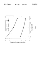
- FIG. 4 shows a relationship between the concentration of the H 2 SiF 6 supersaturated aqueous solution and the SiO 2 deposition rate of the LPD method of the present invention, with the black-square curve representing the boric acid concentration of 0.01M and the black-circle curve representing the boric acid concentration of 0.0075M.
- FIG. 5 shows the current-voltage (I-V) characteristics of the gallium arsenide substrate with the silicon dioxide layer formed thereon by the method of the present invention.
- the method of the present invention employs a chemical treatment capable of forming a number of OH bonds on the surface of the substrate so as to facilitate the growth of the silicon dioxide layer on the substrate by LPD.
- the chemical treatment preferably is able to be carried out at room temperature so that the entire process of growing the silicon dioxide layer on the surface of the substrate can be completed at an extremely low temperature, thereby enhancing the efficiency of the LPD method in improving the process flexibility of the IC preparation at low temperature.
- the chemical treatment is carried out by immersing a III-V compound substrate in an alkaline aqueous solution, such as ammonium hydroxide or hydrogen peroxide.
- a gallium arsenide (GaAs) substrate was chemically treated such that a silicon dioxide layer could be grown by LPD on the modified surface of the GaAs substrate having a 100-orientation and a resistivity of 2.0-2.8 ⁇ 10 -3 ⁇ -cm.
- the GaAs substrate Prior to the chemical treatment, the GaAs substrate was cleaned by immersing the GaAs substrate in acetone for 10 minutes. The GaAs substrate was then removed from the acetone and was once again immersed in methanol for ten minutes. The GaAs substrate was removed from the methanol and was subsequently rinsed with pure water (19 M ⁇ -cm) for five minutes.
- GaO x gallium oxide
- the LPD of the present invention was carried out a supersaturated H 2 SiF 6 aqueous solution, which was prepared by dissolving silicon dioxide powder in a 3.09M H 2 SiF 6 aqueous solution such that a saturated H 2 SiF 6 aqueous solution was formed by agitation at room temperature.
- the undissolved silicon dioxide powder was removed from the saturated H 2 SiF 6 aqueous solution by filtration.
- To 45 ml of the saturated H 2 SiF 6 aqueous solution 38.43 ml of water was added, and the resulting solution was stirred for several minutes.
- the chemically-treated GaAs substrate was immediately immersed in the freshly-prepared supersaturated H 2 SiF 6 aqueous solution at 40° C. for 1.5 hours for growing a silicon dioxide layer on the GaAs substrate by deposition.
- the GaAs substrate was removed from the supersaturated H 2 SiF 6 aqueous solution to facilitate the measuring of thickness and refractive index of the silicon dioxide layer formed on the GaAs substrate.
- the measurements of thickness and refractive index of the silicon dioxide were done by an ellipsometer.
- the growth rate of the silicon dioxide layer is about 1265 ⁇ /hr while the refractive index of the silicon dioxide layer is in the range of 1.37-1.41.
- the method of the present invention has inherent advantages. For example, a flat and uniform interface was formed between the GaAs substrate and the SiO 2 layer. In addition, the SiO 2 layer was formed on the GaAs substrate in a layer-upon-layer pattern without forming islands.
- the AES depth profile of the GaAs substrate reveals that a substantially constant molar ratio between silicon and oxygen atoms exists from the surface of the SiO 2 layer towards the area contiguous to the interface.
- the gallium atoms diffuse outwards from the surface of the gallium arsenide while the silicon atoms diffuse inwards.
- the molar ratio of the silicon atoms and the oxygen atoms is smaller than 1/2 in the interface, with the implication being that a thin oxide layer exists in the vicinity of the interface to enable the growth of the silicon dioxide layer on the gallium arsenide substrate.
- the chemical treatment of the surface of the gallium arsenide substrate results in an increase in the OH bonds on the substrate surface so as to promote the growth of the thin oxide layer in the vicinity of the interface.
- the deposition rate of SiO 2 is not directly proportional to the concentration of H 2 SiF 6 , on the condition that other parameters are kept constant. This is due to the fact that the reactant is not provided with a metastable potential for depositing the silicon dioxide. However, it must be noted that the deposition rate of the silicon dioxide increases as the concentration of the boric acid contained in the supersaturated H 2 SiF 6 aqueous solution is increased.
- the GaAs-based semiconductor device made by the method of the present invention has a leakage current of 40 ⁇ 10 -9 A at -5 V and a breakdown electric field of 7.6 MV/cm.
- the chemical treatment of the surface of the GaAs substrate is crucial to the successful growth of the silicon dioxide film on the surface of the GaAs substrate by the LPD method of the present invention.
- Such a GaAs-based semiconductor device made by the LPD method of the present invention has the refractive index ranging between 1.372 and 1.41.
- the deposition rate of the method of the present invention is as high as 1265 ⁇ /hr.
- the LPD method of the present invention can be successfully performed at low temperature.
- the LPD method of the present invention is a cost-effective process for producing a GaAs-based semiconductor device of excellent quality. It is believed that the LPD method of the present invention can be successfully used to grow the silicon dioxide film on the zincblende III-V semiconductor substrate.
Abstract
Description
ΔH+H.sub.2 SiF.sub.6 +2H.sub.2 O←→6HF+SiO.sub.2 ↓(1)
H.sub.3 BO.sub.3 +4HF←→BF.sub.4 +H.sub.3 O.sup.+ +2H.sub.2 O(2)
NH.sub.4 OH+HF←→NH.sub.4.sup.+ +F.sup.- +H.sub.2 O(3)
Claims (16)
Applications Claiming Priority (2)
| Application Number | Priority Date | Filing Date | Title |
|---|---|---|---|
| TW86104394 | 1997-04-03 | ||
| TW086104394A TW337592B (en) | 1997-04-03 | 1997-04-03 | Process of depositing silicon dioxide on a group III-V semiconductor substrate by ammoniation treatment |
Publications (1)
| Publication Number | Publication Date |
|---|---|
| US5998304A true US5998304A (en) | 1999-12-07 |
Family
ID=21626521
Family Applications (1)
| Application Number | Title | Priority Date | Filing Date |
|---|---|---|---|
| US08/922,186 Expired - Lifetime US5998304A (en) | 1997-04-03 | 1997-09-02 | Liquid phase deposition method for growing silicon dioxide film on III-V semiconductor substrate treated with ammonium hydroxide |
Country Status (2)
| Country | Link |
|---|---|
| US (1) | US5998304A (en) |
| TW (1) | TW337592B (en) |
Cited By (3)
| Publication number | Priority date | Publication date | Assignee | Title |
|---|---|---|---|---|
| US6225239B1 (en) * | 1997-09-30 | 2001-05-01 | Sharp Kabushiki Kaisha | Organic films and a process for producing fine pattern using the same |
| US20040137753A1 (en) * | 2003-01-15 | 2004-07-15 | Industrial Technology Research Institute | Method for low temperature liquid-phase deposition and method for cleaning liquid-deposition apparatus |
| CN103695875A (en) * | 2013-12-06 | 2014-04-02 | 湖洲三峰能源科技有限公司 | Chemical composition for accelerating growth of silicon oxide on surface of substrate |
Citations (4)
| Publication number | Priority date | Publication date | Assignee | Title |
|---|---|---|---|---|
| US5326720A (en) * | 1990-10-25 | 1994-07-05 | Nippon Sheet Glass Co., Ltd. | Method for producing silicon dioxide film which prevents escape of Si component to the environment |
| US5378960A (en) * | 1989-08-18 | 1995-01-03 | Galileo Electro-Optics Corporation | Thin film continuous dynodes for electron multiplication |
| US5516721A (en) * | 1993-12-23 | 1996-05-14 | International Business Machines Corporation | Isolation structure using liquid phase oxide deposition |
| US5650361A (en) * | 1995-11-21 | 1997-07-22 | The Aerospace Corporation | Low temperature photolytic deposition of aluminum nitride thin films |
-
1997
- 1997-04-03 TW TW086104394A patent/TW337592B/en not_active IP Right Cessation
- 1997-09-02 US US08/922,186 patent/US5998304A/en not_active Expired - Lifetime
Patent Citations (4)
| Publication number | Priority date | Publication date | Assignee | Title |
|---|---|---|---|---|
| US5378960A (en) * | 1989-08-18 | 1995-01-03 | Galileo Electro-Optics Corporation | Thin film continuous dynodes for electron multiplication |
| US5326720A (en) * | 1990-10-25 | 1994-07-05 | Nippon Sheet Glass Co., Ltd. | Method for producing silicon dioxide film which prevents escape of Si component to the environment |
| US5516721A (en) * | 1993-12-23 | 1996-05-14 | International Business Machines Corporation | Isolation structure using liquid phase oxide deposition |
| US5650361A (en) * | 1995-11-21 | 1997-07-22 | The Aerospace Corporation | Low temperature photolytic deposition of aluminum nitride thin films |
Cited By (4)
| Publication number | Priority date | Publication date | Assignee | Title |
|---|---|---|---|---|
| US6225239B1 (en) * | 1997-09-30 | 2001-05-01 | Sharp Kabushiki Kaisha | Organic films and a process for producing fine pattern using the same |
| US20040137753A1 (en) * | 2003-01-15 | 2004-07-15 | Industrial Technology Research Institute | Method for low temperature liquid-phase deposition and method for cleaning liquid-deposition apparatus |
| US6803329B2 (en) * | 2003-01-15 | 2004-10-12 | Industrial Technology Research Institute | Method for low temperature liquid-phase deposition and method for cleaning liquid-phase deposition apparatus |
| CN103695875A (en) * | 2013-12-06 | 2014-04-02 | 湖洲三峰能源科技有限公司 | Chemical composition for accelerating growth of silicon oxide on surface of substrate |
Also Published As
| Publication number | Publication date |
|---|---|
| TW337592B (en) | 1998-08-01 |
Similar Documents
| Publication | Publication Date | Title |
|---|---|---|
| KR100202003B1 (en) | Method of forming oxide film on surface of semiconductor substrate | |
| KR900007686B1 (en) | Vapor-phase growth process | |
| US5728625A (en) | Process for device fabrication in which a thin layer of cobalt silicide is formed | |
| US4540607A (en) | Selective LPCVD tungsten deposition by the silicon reduction method | |
| JP3117110B2 (en) | MOS device manufacturing method for boron diffusion | |
| US20030060057A1 (en) | Method of forming ultrathin oxide layer | |
| US5876796A (en) | Process for selectively depositing a refractory metal silicide on silicon, and silicon wafer metallized using this process | |
| JP2002502126A (en) | Method for forming semiconductor device | |
| US7972922B2 (en) | Method of forming a semiconductor layer | |
| Hsieh et al. | Silicon homoepitaxy by rapid thermal processing chemical vapor deposition (RTPCVD)—A review | |
| JP2770544B2 (en) | Method of manufacturing MIS type semiconductor device | |
| JPH05217893A (en) | Manufacture of semiconductor substrate | |
| JPH0845947A (en) | Thermal treatment method of silicon substrate | |
| US6372581B1 (en) | Process for nitriding the gate oxide layer of a semiconductor device and device obtained | |
| US5998304A (en) | Liquid phase deposition method for growing silicon dioxide film on III-V semiconductor substrate treated with ammonium hydroxide | |
| Shelton et al. | Ultrasmooth GaN etched surfaces using photoelectrochemical wet etching and an ultrasonic treatment | |
| US6451660B1 (en) | Method of forming bipolar transistors comprising a native oxide layer formed on a substrate by rinsing the substrate in ozonated water | |
| Kuech et al. | The effect of surface preparation on the production of low interfacial charge regrown interfaces | |
| US5374481A (en) | Polyemitter structure with improved interface control | |
| US6306212B1 (en) | Gallium arsenide semiconductor devices fabricated with insulator layer | |
| US6004886A (en) | Liquid phase deposition method for forming silicon dioxide film on HGCDTE or other II-VI semiconductor substrate | |
| US5366934A (en) | Method for sulfide surface passivation | |
| Aoyama et al. | Surface cleaning for Si epitaxy using photoexcited fluorine gas | |
| Hsieh et al. | Shallow junction formation by dopant diffusion from in situ doped polycrystalline silicon chemically vapor deposited in a rapid thermal processor | |
| Biedenbender et al. | Chemical Nature of Silicon Nitride‐Indium Phosphide Interface and Rapid Thermal Annealing for InP MISFETs |
Legal Events
| Date | Code | Title | Description |
|---|---|---|---|
| AS | Assignment |
Owner name: NATIONAL SCIENCE COUNCIL, TAIWAN Free format text: ASSIGNMENT OF ASSIGNORS INTEREST;ASSIGNORS:HOUNG, MAU-PHON;WANG, YEONG-HER;HUANG, CHIEN-JUNG;REEL/FRAME:010214/0573 Effective date: 19970826 |
|
| STCF | Information on status: patent grant |
Free format text: PATENTED CASE |
|
| FEPP | Fee payment procedure |
Free format text: PAYOR NUMBER ASSIGNED (ORIGINAL EVENT CODE: ASPN); ENTITY STATUS OF PATENT OWNER: LARGE ENTITY |
|
| FPAY | Fee payment |
Year of fee payment: 4 |
|
| FEPP | Fee payment procedure |
Free format text: PAYER NUMBER DE-ASSIGNED (ORIGINAL EVENT CODE: RMPN); ENTITY STATUS OF PATENT OWNER: LARGE ENTITY Free format text: PAYOR NUMBER ASSIGNED (ORIGINAL EVENT CODE: ASPN); ENTITY STATUS OF PATENT OWNER: LARGE ENTITY |
|
| FEPP | Fee payment procedure |
Free format text: PAYER NUMBER DE-ASSIGNED (ORIGINAL EVENT CODE: RMPN); ENTITY STATUS OF PATENT OWNER: LARGE ENTITY |
|
| FPAY | Fee payment |
Year of fee payment: 8 |
|
| FPAY | Fee payment |
Year of fee payment: 12 |