US6001203A - Production process of liquid crystal display panel, seal material for liquid crystal cell and liquid crystal display - Google Patents
Production process of liquid crystal display panel, seal material for liquid crystal cell and liquid crystal display Download PDFInfo
- Publication number
- US6001203A US6001203A US08/988,195 US98819597A US6001203A US 6001203 A US6001203 A US 6001203A US 98819597 A US98819597 A US 98819597A US 6001203 A US6001203 A US 6001203A
- Authority
- US
- United States
- Prior art keywords
- curing
- seal material
- liquid crystal
- crystal display
- meth
- Prior art date
- Legal status (The legal status is an assumption and is not a legal conclusion. Google has not performed a legal analysis and makes no representation as to the accuracy of the status listed.)
- Expired - Lifetime
Links
Images


Classifications
-
- G—PHYSICS
- G02—OPTICS
- G02F—OPTICAL DEVICES OR ARRANGEMENTS FOR THE CONTROL OF LIGHT BY MODIFICATION OF THE OPTICAL PROPERTIES OF THE MEDIA OF THE ELEMENTS INVOLVED THEREIN; NON-LINEAR OPTICS; FREQUENCY-CHANGING OF LIGHT; OPTICAL LOGIC ELEMENTS; OPTICAL ANALOGUE/DIGITAL CONVERTERS
- G02F1/00—Devices or arrangements for the control of the intensity, colour, phase, polarisation or direction of light arriving from an independent light source, e.g. switching, gating or modulating; Non-linear optics
- G02F1/01—Devices or arrangements for the control of the intensity, colour, phase, polarisation or direction of light arriving from an independent light source, e.g. switching, gating or modulating; Non-linear optics for the control of the intensity, phase, polarisation or colour
- G02F1/13—Devices or arrangements for the control of the intensity, colour, phase, polarisation or direction of light arriving from an independent light source, e.g. switching, gating or modulating; Non-linear optics for the control of the intensity, phase, polarisation or colour based on liquid crystals, e.g. single liquid crystal display cells
- G02F1/133—Constructional arrangements; Operation of liquid crystal cells; Circuit arrangements
- G02F1/1333—Constructional arrangements; Manufacturing methods
- G02F1/1339—Gaskets; Spacers; Sealing of cells
-
- C—CHEMISTRY; METALLURGY
- C09—DYES; PAINTS; POLISHES; NATURAL RESINS; ADHESIVES; COMPOSITIONS NOT OTHERWISE PROVIDED FOR; APPLICATIONS OF MATERIALS NOT OTHERWISE PROVIDED FOR
- C09J—ADHESIVES; NON-MECHANICAL ASPECTS OF ADHESIVE PROCESSES IN GENERAL; ADHESIVE PROCESSES NOT PROVIDED FOR ELSEWHERE; USE OF MATERIALS AS ADHESIVES
- C09J163/00—Adhesives based on epoxy resins; Adhesives based on derivatives of epoxy resins
- C09J163/10—Epoxy resins modified by unsaturated compounds
-
- G—PHYSICS
- G02—OPTICS
- G02F—OPTICAL DEVICES OR ARRANGEMENTS FOR THE CONTROL OF LIGHT BY MODIFICATION OF THE OPTICAL PROPERTIES OF THE MEDIA OF THE ELEMENTS INVOLVED THEREIN; NON-LINEAR OPTICS; FREQUENCY-CHANGING OF LIGHT; OPTICAL LOGIC ELEMENTS; OPTICAL ANALOGUE/DIGITAL CONVERTERS
- G02F1/00—Devices or arrangements for the control of the intensity, colour, phase, polarisation or direction of light arriving from an independent light source, e.g. switching, gating or modulating; Non-linear optics
- G02F1/01—Devices or arrangements for the control of the intensity, colour, phase, polarisation or direction of light arriving from an independent light source, e.g. switching, gating or modulating; Non-linear optics for the control of the intensity, phase, polarisation or colour
- G02F1/13—Devices or arrangements for the control of the intensity, colour, phase, polarisation or direction of light arriving from an independent light source, e.g. switching, gating or modulating; Non-linear optics for the control of the intensity, phase, polarisation or colour based on liquid crystals, e.g. single liquid crystal display cells
- G02F1/133—Constructional arrangements; Operation of liquid crystal cells; Circuit arrangements
- G02F1/1333—Constructional arrangements; Manufacturing methods
- G02F1/1341—Filling or closing of cells
- G02F1/13415—Drop filling process
Definitions
- the present invention relates to seal materials for liquid crystal display apparatus that are used as display apparatus for electronic devices, a process for producing the liquid crystal display apparatus using the liquid crystal seal materials, and liquid crystal display apparatus comprising a liquid crystal panel sealed with the liquid crystal seal material in the production process.
- General production methods for liquid crystal display apparatus having a liquid crystal display panel comprising two transparent substrates, to which electrodes have been applied with an alignment treatment, with liquid crystal sealed therebetween include a method of attaching two substrates to each other via a spacer by the substrates alignment, compressing by a press plate, a weight, or a vacuum packing to provide a uniform cell gap, and curing by heat as disclosed in JP-A-59-232315 or JP-B-6-68669.
- liquid crystal seal materials used for attaching the two substrates and sealing a liquid crystal include one-pack type thermosetting epoxy resins such as "STRUCTBOND XN-21-F" produced by MITSUI TOATSU Chemical, INC.
- Such seal materials containing a thermosetting epoxy resin have problems such as dislocation of the two substrates that are preliminarily aligned and attached, generation of substrate warping due to a high curing temperature (150° C.), and a long curing time.
- an ultraviolet ray curing type seal material a seal material containing both an ultraviolet ray curing type component and a thermosetting type component, and a double type seal material overlapping a thermosetting curing type seal and a ultraviolet ray curing type component can be used.
- ultraviolet ray curing type seal materials include those containing (meth)acrylic acid monomer capable of curing by radical polymerization.
- a "(Meth)acrylic acid monomer” herein denotes a compound comprising at least one selected from the group consisting of acrylic acid monomer, acrylic acid ester monomer, methacrylic acid monomer, methacrylic acid ester monomer and derivatives thereof.
- JP-A-7-13173 and JP-A-7-13174 In order to prevent such curing shrinkage, use of a modified urethane acrylate is advocated in JP-A-7-13173 and JP-A-7-13174.
- urethane acrylate expands by heat and is not heat resistant.
- the annealing process conducted to ensure the uniform display plane of the liquid crystal display apparatus since the annealing needs to be carried out at the nematic-isotropic phase transition temperature (generally from 80° C. to 120° C. or higher), seal materials containing urethane acrylate expand to cause problems such as generation of threshold voltage irregularity caused by the gap height in the vicinity of sealed portions of the liquid crystal panel.
- seal materials containing both an ultraviolet ray curing type component and a thermosetting type component having an improved curing rate include those disclosed in JP-A-4-11223 and JP-A-6-160872.
- thermosetting type component examples include a resin obtained by polymerizing (meth)acrylic acid monomer or oligomer as the ultraviolet ray curing component, and an epoxy resin as the thermosetting type component, the epoxy resin disturbs the radical polymerization of (meth)acrylic acid monomer or oligomer in ultravioletray curing to require a great amount of ultraviolet ray energy.
- the thermosetting component is an epoxy resin, thermosetting at a high temperature over a long time becomes necessary, which causes problems such as decline of yield in production caused by warpage of glass substrates.
- a seal material polymerized by a radical polymerization and capable of ultraviolet ray curing is required.
- Another object of this invention is to provide a liquid crystal seal material, including both an ultraviolet ray curing component and a thermosetting component, used for a liquid crystal panel of a liquid crystal display apparatus having excellent adherence and moisture resistance without disturbing radical polymerization in ultraviolet ray curing, without the need of thermosetting at a high temperature over a long time, without the chance of poor alignment of the liquid crystal, and capable of being used in a dropping production process by containing only (meth)acrylic acid monomer or oligomer polymerized by radical polymerization as the monomer or oligomer component to be polymerized, and a liquid crystal display apparatus with high display quality and reliability comprising a liquid crystal display panel sealed by the liquid crystal seal material.
- a production process of liquid crystal display apparatus of the present invention comprises the steps of:
- Reduced pressure atmosphere herein denotes a pressure of about 0.4 to 1.0 Torr.
- the weight ratio of the ultraviolet ray curing resin component and the thermosetting resin component is from 60:40 to 90:10.
- a production process for a liquid crystal display panel of the present invention comprises the steps of forming a sealing resin composition containing a curing resin and a curing agent to initiate curing of the curing resin at a portion to be sealed on the surface of a first transparent substrate on which electrodes have been installed,
- the curing agent in the sealing resin composition comprises an ultraviolet ray curing agent to initiate the curing of the curing resin by the ultraviolet ray irradiation and a thermosetting agent to initiate the curing of the curing resin by heating
- the process to cure the curing resin comprises a first process that provides at least 60% and less than 80% of the curing ratio of the curing resin by irradiating an ultraviolet ray to the sealing resin composition, and a second process to increase the curing to at least 80% and less than 100% of the curing ratio of the curing resin by heating the sealing resin composition after the first process.
- the curing agent in the sealing resin composition comprises an ultraviolet ray curing agent to initiate the curing of the curing resin by the ultraviolet ray irradiation and a particle type thermosetting agent to initiate the curing of the curing resin by heating, wherein the process to cure the curing resin comprises a first process that provides at least 50% and less than 80% of the curing ratio of the curing resin by irradiating an ultraviolet ray to the sealing resin composition and a second process to increase the curing to at least 80% and less than 100% of the curing ratio of the curing resin by heating the sealing resin composition after the first process.
- one pair of large-area transparent substrates with electrodes are used to install a plurality of the liquid crystal display panels so that the pair of large-area transparent substrates with electrodes can be divided into a plurality of the liquid crystal display panels.
- the liquid crystal display panel is formed by dropping liquid crystal between the step of forming a seal and the step of attaching the two substrates with electrodes.
- a seal material for liquid crystal display panel of the present invention comprises an ultraviolet ray curing component and a thermosetting component.
- the seal material may contain epoxy (meth)acrylate, (meth)acrylic acid ester, an optical initiator, a thermosetting agent and an inorganic filler as essential components, wherein as the (meth)acrylic acid ester, 5 to 10 weight % based on the seal material of (meth)acrylic acid ester having a plurality of (meth)acrylic acid residues per molecule is included and 2 to 10 weight % based on the seal material of (meth)acrylic acid ester having one (meth)acrylic acid residue per molecule is included.
- the epoxy (meth)acrylate is present in an amount of 40 to 70 weight % based on the seal material and is bisphenol A type or novolak type.
- the optical initiator is present in an amount of 3 to 5 weight % based on the seal material and is one selected from the group consisting of an acetophenone type optical initiator, a benzoin type optical initiator and a benzophenone type optical initiator.
- thermosetting agent is present in an amount of 2 to 5 weight % based on the seal material and is one selected from the group consisting of hydrazide, aromatic group amine, acid anhydride and bimidazole.
- thermosetting agent is a particle type thermosetting agent having an average particle size of 3 ⁇ m or smaller.
- a silane coupling agent is further comprised and present in an amount of 2 to 7 weight % based on the seal material, and is one selected from the group consisting of glycidyl ethoxy silane and glycidyl methoxy silane.
- the inorganic filler has an average particle size of 1.5 ⁇ m or smaller, and is present in an amount of 8 to 20 weight % based on the seal material and is one selected from the group consisting of hydrated magnesium silicate, calcium carbonate, aluminum carbonate and silica.
- a liquid crystal display panel of the present invention comprises two transparent substrates with electrodes attached to each other by sealing with a resin composition mainly comprising a curing resin and with curing ratio of 80% or more.
- the mixing ratio of the ultraviolet ray curing resin component and the thermosetting resin component is 60:40 to 90:10.
- the curing agent for curing the curing resin is a radical polymerization initiator to initiate the radical polymerization of the curing resin.
- the present invention relates to a liquid crystal display panel comprising two substrates with electrodes having a sealed liquid crystal therebetween, of which production process comprises a step of a seal forming process to form a seal portion at the edge portion of at least one of the substrates of the liquid crystal display panel on the electrode side surface by a seal comprising a ultraviolet ray curing agent component and a thermosetting agent component, a first curing step that provides at least 50 to 60% of the curing ratio of the curing resin by irradiating an ultraviolet ray to the sealing resin composition and a second step to increase the curing to at least 80% of the curing ratio of the curing resin by heating the sealing resin composition.
- thermosetting seals Since a seal material containing both an ultraviolet ray curing component and a thermosetting component and a temporary hardening is conducted by irradiating an ultraviolet ray to the sealing portion of the cell, unlike conventional thermosetting seals, problems such as poor alignment caused by discharge of the seal material due to viscosity decline thereof, cutoff of the seal material and alignment dislocation of the substrates do not occur.
- the curing ratio of the ultraviolet ray curing component of the seal material after the ultraviolet ray curing is at least 50% to 60%, increase of voltage due to discharge of the seal material into the liquid crystal and a poor alignment of the liquid crystal can be prevented.
- the curing ratio of the seal material after main hardening is at least 80%, peeloff of the panel corner portion at the time of cutting off the substrates can be prevented to produce a reliable liquid crystal display apparatus with a high yield.
- a seal material for liquid crystal display panel of the present invention comprising a ultraviolet ray curing component and a thermosetting component contains epoxy (meth)acrylate, (meth)acrylic acid ester, an optical initiator, a thermosetting agent and an inorganic filler as the essential components, wherein as the (meth)acrylic acid ester, 5 to 10 weight % based on the seal material of (meth)acrylic acid ester having a plurality of (meth)acrylic acid residues per molecule is included and 2 to 10 weight % based on the seal material of (meth)acrylic acid ester having one (meth)acrylic acid residue per molecule is included.
- the epoxy (meth)acrylate is present in an amount of 40 to 70 weight % based on the seal material and is a bisphenol A type or novolak type.
- the optical initiator is present in an amount of 3 to 5 weight % based on the seal material and is one selected from the group consisting of an acetophenone type optical initiator, a benzoin type optical initiator and a benzophenone type optical initiator.
- thermosetting agent is present in an amount of 2 to 5 weight % based on the seal material and is one selected from the group consisting of hydrazide, aromatic group amine, acid anhydride and imidazole.
- thermosetting agent is a particle type thermosetting agent having an average particle size of 3 ⁇ m or smaller.
- the silane coupling agent is present in an amount of 2 to 7 weight % based on the seal material and is one selected from the group consisting of glycidyl ethoxy silane and glycidyl methoxy silane.
- the inorganic filler having an average particle size of 1.5 ⁇ m or smaller is present in an amount of 8 to 20 weight % based on the seal material and is one selected from the group consisting of hydrated magnesium silicate, calcium carbonate, aluminum carbonate and silica.
- the above mentioned seal material can be preferably used as a seal material for a liquid crystal display panel produced by a production process comprising a step of dropping liquid crystal between a step of forming the seal material and a step of attaching the two substrates with electrodes.
- a liquid crystal display apparatus of the present invention comprises a liquid crystal display panel containing liquid crystal sealed by any of the above mentioned seal materials.
- the liquid crystal display panel is produced by a production process comprising a step of dropping liquid crystal between a step of forming a seal and a step of attaching the two substrates with electrodes.
- the seal material of the present invention which comprises an ultraviolet ray curing component and a thermosetting component, epoxy (meth)acrylate, (meth)acrylic acid ester, an optical initiator, and a thermosetting agent comprising a thermosetting agent for crosslinking a resin component polymerized by radical polymerization by irradiating an ultraviolet ray to the ultraviolet ray curing component.
- a seal material of the present invention does not include epoxy resin, heating over a long time is not necessary to cure the epoxy resin, so as not to deteriorate the viscosity of the seal material by heating, the alignment dislocation of the substrates after attaching or the substrate warpage will not occur. Further, since epoxy resin is not included, the risk of disturbing the radical polymerization of epoxy (meth)acrylate or (meth)acrylic acid ester in the ultraviolet ray curing is eliminated.
- a liquid crystal display apparatus comprising a liquid crystal panel having liquid crystal sealed with the above mentioned liquid crystal seal material has excellent properties in adhesion and moisture resistance to provide good display quality and reliability without the risk of poor alignment of the liquid crystal or increase of the electric current value.
- the seal material of the present invention cures by radical polymerization and the reaction ratio in ultraviolet ray curing is high, even when a dropping process is employed, namely, a seal material is formed on one of two substrates with electrodes applied with alignment treatment and the substrate is attached to the other substrate via a spacer means before dropping liquid crystal therebetween, the alignment condition or electric characteristic of the liquid crystal will not be affected significantly.
- a thermosetting agent to polymerize at a temperature below the annealing temperature of the liquid crystal panel, even when thermosetting a seal material after ultraviolet ray curing, production efficiency will not decline. Accordingly, a liquid crystal display apparatus with a good display quality can be efficiently provided even with a dropping process.
- the epoxy (meth)acrylate component has comparatively small heat expansion and a fast polymerization
- a dropping process namely a process in which a seal material is provided on a substrate with electrodes applied with the alignment treatment, opposing substrates are attached via a spacer means and liquid crystal is dropped therebetween
- it is effective in preventing poor alignment or increase of the electric current value caused by discharge of the seal material component into the liquid crystal by the contact of the uncured liquid seal material and the liquid crystal.
- epoxy (meth)acrylate is, in general, available in the form of oligomer, it is used in a form of an oligomer as a component material in this invention.
- a (meth)acrylic acid ester containing a plurality of (meth)acrylic acid residues per molecule contributes to increasing the curing density, facilitating thermosetting, and achieving a seal material with reliability in a high temperature.
- the component is contained at less than 5 weight % based on the seal material, the crosslinking density becomes insufficient to provide a liquid crystal display apparatus having a high themosetting reliability and moisture resistance.
- the amount exceeds 10 weight %, the curing shrinkage becomes significant, preventing the achievement of a good attaching property.
- (meth)acrylic acid ester having one (meth)acrylic acid residue per molecule has a comparatively small amount of curing shrinkage, it is preferable as a component to curb the curing shrinkage. Further, it provides a solvent of epoxy (meth)acrylate in a stage of a monomer before polymerization and provides a viscosity adjustment agent to enable proper adjustment of the viscosity of the seal material when the seal material is applied to a substrate by printing. When the ratio of the component in the seal material is 2 weight % or less, the curing shrinkage of the seal material becomes too large to achieve a liquid crystal display apparatus having a high adherence.
- the ratio exceeds 10 weight %, the crosslinking density becomes too low to achieve a liquid crystal display apparatus having high heat resistance and moisture resistance. Further, by including too much amount, the uncured component becomes liable to be discharged into the liquid crystal to cause problems such as poor alignment and increase of the electric current value.
- An optical initiator provides a radical generation source, which is necessary for ultraviolet ray polymerization of the above mentioned (meth)acrylic monomer or oligomer component.
- a thermosetting agent mainly contributes to the crosslinking by heat and curing by heat of polymer component yielded by the above mentioned ultraviolet ray polymerization to achieve improvement of adherence and heat resistance.
- a silane coupling agent is effective in further improving the moisture resistance.
- An inorganic filler contributes to adherence such as improvement of peeling strength as well as adjustment of viscosity of the seal material.
- seal materials of the present invention include the above mentioned components, even though they cure by the radical polymerization, they have excellent adherence and moisture resistance to provide high display quality and reliability.
- epoxy (meth)acrylate is bisphenol A type or novolak type and contained in a liquid crystal seal material by 40 to 70 weight %.
- a bisphenol A type or novolak type epoxy (meth)acrylate having a viscosity adjustable to have an appropriate viscosity at the time of applying the seal material by printing is preferable. Further, one not liable to expand by heat compared with a modified urethane acrylate is preferable.
- the ratio of 40 to 70 weight % eliminates the problem such as curing shrinkage caused by the increase of the other monomer component ratio, poor alignment of the liquid crystal, increase of the electric current value, high or low viscosity of the seal material when being applied by printing, it is preferable.
- an optical initiator selected from the group consisting of acetophenone type optical initiator, benzoin type optical initiator and benzophenone type optical initiator, polymerization can proceed well with a wavelength of an ordinary ultraviolet ray lamp. Further, since such optical initiators have a long pot life to eliminate the risk of overpolymerization during adjustment of the seal material or applying the seal material on a substrate by printing, they are preferable. If the ratio of an optical initiator is too low, since the ultraviolet ray curing cannot proceed well, the uncured component would discharge into the liquid crystal to cause poor alignment of the liquid crystal. On the other hand, if the ratio is too high, since the ultraviolet ray curing cannot proceed sufficiently, problems may occur such as discharge of surplus optical initiator into the liquid crystal to increase the electric current value. Therefore it is preferable that 3 to 5 weight % of an optical initiator is contained in the liquid crystal seal material.
- thermosetting agent selected from the group consisting of hydrazide, aromatic group amine, acid anhydride and imidazole, since such thermosetting agents have a curing temperature lower than a usual decomposition point to avoid the risk of deteriorating the liquid crystal by heat. Further, since such thermosetting agents have a long pot life, namely, 8 hours or more at a room temperature, they avoid the risk of excessive crosslinking polymerization of the thermosetting agent during the adjustment of the seal material or the application of the seal material onto the substrate by printing.
- thermosetting agent having an average particle size of 3 ⁇ m or less has a long pot life and does not prevent the radical polymerization in the ultraviolet ray curing, it is preferable. Since an average particle size is 3 ⁇ m or less, and it is smaller than the gap between two substrates of liquid crystal panel to be adjusted by a spacer means, and thus the risk of causing gap defect is prevented, it is preferable.
- the lower limit of the average particle size of the thermosetting agent is not particularly limited, but it is in general, about 1 ⁇ m.
- a silane coupling agent selected from the group consisting of glycidyl ethoxy silane and glycidyl methoxy silane has a further improvement effect of moisture resistance, it is preferable. If the ratio of the silane coupling agent is too low, moisture resistance of the liquid crystal panel cannot be improved. If the ratio of the silane coupling agent is too high, poor alignment of the liquid crystal may occur due to discharge of the seal material into the liquid crystal. Therefore, it is preferable to have a silane coupling agent in the liquid crystal seal material in an amount of 2 to 7 weight % based on the seal material to avoid such problems.
- Inorganic fillers selected from the group consisting of hydrated magnesium silicate, calcium carbonate, aluminum oxide and silica are used and those having an average particle size of 1.5 ⁇ m or less are comparatively well accessible. They improve adherence and their viscosity can be adjusted easily at the time of printing application of the seal material, and thus they are preferable. By having an inorganic filler having an average particle size of 1.5 ⁇ m or smaller, it can disperse well in the seal material, and the average particle size is smaller than the gap of the two substrates of the liquid crystal panels to be adjusted by a spacer means, gap defect cannot occur, and thus it is preferable.
- the lower limit of the average particle size of the inorganic filler is not particularly limited, but in general, a small one of about 15 ⁇ m can be preferably used. If the ratio of an inorganic filler is too low, adhesion cannot be sufficiently improved. If the ratio is too high, it hampers applying the seal material to the substrate by printing, and further a predetermined distance of the gap between the two substrates cannot be maintained. Therefore it is preferable to have an inorganic filler in the seal material in an amount of 8 to 20 weight % to avoid the problems.
- liquid crystal display apparatus having a good display quality can be obtained without problems such as deteriorating the alignment of the liquid crystal caused by discharge of the seal material or cutting off of the seal material after attaching the substrates in the dropping method.
- FIG. 1 is a perspective view illustrating the attaching process of two substrates with electrodes applied with alignment treatment of one embodiment of the present invention.
- FIG. 2 is a diagram illustrating the temporary hardening process of the liquid crystal seal material by ultraviolet ray irradiation of one embodiment of the present invention.
- FIG. 3 is a perspective view illustrating the liquid crystal display panel produced by the production process of one embodiment of the present invention.
- FIG. 4 is a partial enlarged view of the seal portion of the liquid crystal display panel of FIG. 3.
- FIG. 5 is a sectional diagram of a liquid crystal display panel for a liquid crystal display apparatus of one embodiment of the present invention.
- FIG. 6 is a plane view illustrating the peel strength test of a substrate of the liquid crystal display panel of one embodiment of the present invention.
- FIG. 7 is a side view illustrating the peel strength test of a substrate of the liquid crystal display panel of one embodiment of the present invention.
- FIG. 8 is a perspective view illustrating the process of dropping liquid crystal in a dropping process of a production process of a liquid crystal display panel of one embodiment of the present invention.
- FIG. 9 is a sectional view illustrating the process of attaching a substrate to which liquid crystal was dropped to an opposing substrate with a spacer material located thereon.
- Example 1 of the production process of liquid crystal display panels of the present invention includes as the essential elements a process to form a seal portion, a process to attach substrates with a temporary hardening process and a main hardening process of the liquid crystal seal material.
- spacer materials any material that can determine the gap between substrates can be used. Examples include glass fibers, resin beads, and glass beads.
- the spacer materials can be contained only in the seal material or only in the effective display portion, but it is preferable to use a certain spacer material respectively in the seal material and in the effective display portion to provide a uniform gap between substrates.
- a resin having an ultraviolet ray curing component and a thermosetting component can be used as a resin for the seal material in the present invention.
- a ultraviolet ray curing component cured by the radical polymerization is preferable since it has little interaction with the liquid crystal.
- a resin of the seal material is preferably a polyfunctional acrylate type resin including bisphenol A type vinyl ester type acrylate oligomer produced by SHOWA HIGHPOLYMER CO., LTD. such as "SP-1563" and "SP-1519” and a polyfunctional methacrylate type resin.
- ultraviolet ray or heat polymerization initiators As components of the liquid seal material of the present invention, ultraviolet ray or heat polymerization initiators, sensitizing agents, reactive diluting agents and polymerization accelerators can be added as needed.
- thermosetting agents of the liquid crystal seal materials of the present invention amine type thermosetting agents such as “EPIKURE Z” and “EPIKURE 150", imidazole type thermosetting agents such as “EPIKURE EMI-24”, acid anhydride type thermosetting agents such as “EPIKURE YH-306” produced by YUKA SHELL EPOXY CO., LTD. and hydrazide type thermosetting agents such as "VDH”, “UDH”, and “LDH” produced by AJINOMOTO CO., LTD. are preferable since they do not have interaction with the liquid crystal and with respect to heating temperature and pot life.
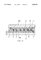
- FIG. 1 is a perspective view illustrating the process of attaching substrates in the vacuum chamber.
- the pressure in the vacuum chamber 6 was reduced to become 1.0 to 0.4 Torr. Then the spacers 5A and 5B were removed to attach the substrates 1A and 1B.
- the vacuum chamber 6 was opened to compress the attached substrates by the atmospheric pressure to produce a cell 7. Since the atmospheric pressure was applied uniformly onto the entire substrate without biased stress, a good cell having a uniform cell gap without alignment dislocation was obtained.
- the display portion of the produced cell was covered with an ultraviolet ray mask 8 to irradiate an ultraviolet ray only to the seal portion to conduct a temporary hardening of the seal material 3 as illustrated in FIG. 2. Further, to improve the adherence of the seal material, main hardening was conducted.
- thermosetting curing By using a seal material using both ultraviolet ray curing and thermosetting curing to allow a temporary hardening of the seal material by ultraviolet ray irradiation after producing a cell, a good straight finishing without discharge or cutoff of the seal material can be obtained as illustrated in FIG. 4. Further, by thermosetting, a seal material having good adherence and moisture resistance was obtained.
- the cell 7 after main hardening was cut to leave electrode terminal portions and the liquid crystal was filled from an opening 9. By closing the opening, a liquid crystal display panel was completed.
- the alignment on the edge of the seal portion of the liquid crystal display panel produced in the above mentioned process was good since the viscosity of the seal material was increased by improving the polymerization degree by conducting a temporary hardening of the seal material by the ultraviolet ray to eliminate the discharge of the seal material into the alignment film.
- the production process of the liquid crystal display panels of this Example is a process of attaching two transparent substrates with electrodes with a liquid crystal seal material to provide a predetermined gap between the two substrates and then filling a liquid crystal into the gap.
- the liquid crystal seal material for the liquid crystal display panel produced in the above mentioned method is a type including both an ultraviolet ray curing type component and a thermosetting type component.
- a resin of the type including both ultraviolet ray curing type component and a thermosetting type component acrylate resins and methacrylate resins which proceed with curing by the radical polymerization can be preferably used. Since a cationic optical initiator is used as the ultraviolet ray curing agent when an epoxy resin is used, a high ultraviolet ray energy is needed and the polymerization speed of an epoxy resin is slow. When a cationic initiator discharges into liquid crystal, the display quality deteriorates by the increase of the electric current value and poor alignment.
- acrylate resins and methacrylate resins examples include “SP-1519” and “SP-1563” produced by SHOWA HIGHPOLYMER CO., LTD.
- optical initiators acetophenone type optical initiators, benzoin type optical initiators and benzophenone type optical initiators can be used.
- optical initiators include "IRGACURE 651” and "IRGACURE 907” produced by CIBA GEIGY JAPAN LTD.
- thermosetting agents aromatic amine type thermosetting agents, imidazole type thermosetting agents, acid anhydride thermosetting agents, hydrazide type thermosetting agents and organic peroxide type thermosetting agents can be used.
- thermosetting agents examples include “EPIKURE Z” and “EPIKURE 150" produced by YUKA SHELL EPOXY CO., LTD.
- imidazole type thermosetting agents examples include “EPIKURE EMI-24” produced by YUKA SHELL EPOXY CO., LTD.
- acid anhydride type thermosetting agents examples include “EPIKURE YH-306” produced by YUKA SHELL EPOXY CO., LTD.
- hydrazide type thermosetting agents examples include “UDH”, “LDH” and “VDH” produced by AJINOMOTO CO., LTD.
- organic peroxide type thermosetting agents examples include “PERBUTYL O", “PERBUTYL 355", “PERBUTYL L”, “PERBUTYL Z” and “PERBUTYL IF” produced by NOF Corporation.
- FIG. 5 is a sectional view illustrating a liquid crystal display panel produced in a production process of the present invention.
- the liquid crystal display panel of this Example has a structure formed by controlling a cell gap by sprinkling glass beads spacer material 2 between two substrates to which electrodes have been applied with an alignment treatment 12A, 12B, then attaching the substrates 12A, 12B to each other with a seal material 3 and sealing a liquid crystal 13 with the seal material 3.
- Numeral 11 in FIG. 5 denotes transparent electrodes formed on the primary surface of the substrates 12A and 12B.
- Numeral 10 is an alignment film formed on the primary surface of the substrates 12A and 12B to cover the transparent electrodes 11. The alignment film 10 does not overlap the region in which the seal material 3 is formed.
- the seal material 3 is a seal material including both an ultraviolet ray curing type component and a thermosetting type component.
- Liquid crystal display panels having the above mentioned structure with various curing conditions of the seal material 3 were produced and the relationship between the curing ratio of the resin and properties of the liquid crystal display panel was examined.
- Table 1 and Table 2 illustrate components of the seal materials of both ultraviolet ray curing and thermosetting used in this Example.
- Table 3 illustrates the components of the ultraviolet ray curing type seal material.
- Table 4 illustrates the relationship between the curing ratio of the curing resin, epoxy acrylate "SP-1563" produced by SHOWA HIGHPOLYMER CO., LTD in the seal material and the curing condition (ultraviolet ray irradiation time).
- the seal material A is the one having the components illustrated in Table 1
- the seal material B is the one having the components illustrated in Table 2
- the seal material C is the one having the components illustrated in Table 3.
- the curing ratio was determined by measuring the amount of change of the carbon-carbon double bond (C ⁇ C) by comparing before and after curing reaction by FT-IR. That is, the curing ratio is the ratio of the reacted C ⁇ C double bond portions based on the C ⁇ C double bond portions of the entire curing resin region.
- Table 5 shows the display property (outside appearance), and Table 6 shows the electric current value at 1 V, 100 Hz.
- HGQ-2000 As the ultraviolet ray lamp used in the ultraviolet ray curing, a high pressure mercury lamp "HGQ-2000" produced by JAPAN STORAGE BATTERY CO., LTD. is used with the irradiation degree of 20 mw of the ultraviolet ray of 420 nm or less to be irrradiated to the seal material.
- thermosetting type agent (EPIKURE Z" produced by YUKA SHELL EPOXY CO., LTD.) is liquid type aromatic group amine, the thermosetting agent tends to elute into the liquid crystal. Therefore, in order to have a display property of a satisfactory level, the curing ratio of the curing resin needs to be 60% or more to prevent the elution of the uncured component and the thermosetting agent of the curing resin into the liquid crystal.
- thermosetting agent produced by AJINOMOTO CO., LTD.
- UDH ultraviolet ray curing type component
- thermosetting agent particle type hydrazide type compound
- the thermosetting agent does not tend to elute into the liquid crystal.
- the ultraviolet ray curing seal material C Table 3 not containing a thermosetting agent, with the curing ratio of the curing resin of 50% or more, the elution of the uncured component and the thermosetting agent into the liquid crystal can be prevented to have a satisfactory display level.
- a particle type thermosetting agent is more advantageous than a liquid type thermosetting agent, since a particle type thermosetting agent can be cured with a shorter time of ultraviolet ray irradiation ato improve the productivity.
- Tables 7 to 9 show the relationship between the curing condition (heating condition) and the curing ratio of the above mentioned seal material A (Table 1), seal material B (Table 2) and seal material C (Table 3), further with a heat curing of the curing resins in various conditions after the above mentioned ultraviolet ray reaction was saturated. Similarly, the curing ratio was determined by measuring the amount of change of the carbon-carbon double bond (C ⁇ C) by FT-IR.
- Table 10 to 12 shows adhesion properties after heat curing.
- FIG. 6 is a plane view illustrating the testing apparatus conducting the peel strength test.
- FIG. 7 is a side view of the tesing apparatus.
- numeral 21 denotes a pressure gauge, a pressing stick 22, a liquid crystal display panel holder 23, a liquid crystal display panel 24 for measuring that comprises an upper substrate 24A and a lower substrate 24B, a liquid crystal display panel support 25, a base 26, and a pulse motor 27.
- the sealing width of the liquid crystal display panel for measuring was 1 mm.
- the liquid crystal display panel for measuring 24 fixed on the base 26 was elevated by the upward movement of the base 26 by means of the pulse motor 27 with the lower substrate 24B pressed by the pressing stick 22.
- the compression power at the time when the lower substrate 24B separates from the upper substrate 24A was measured by the pressure gauge 21 and determined as the peeling strength.
- a seal material including both ultraviolet ray curing type component and thermosetting type component obtains the peeling strength of 5 kgf and more with the curing ratio of the curing resin of 80% or more so as to avoid the risk of the substrate peeling off in a following cutting process to divide a sheet into cells.
- an ultraviolet ray curing type seal material can not improve adhesion since it can not change the curing ratio after heating. Therefore, with only an ultraviolet ray curing type sealing material, a sufficient adhesion property of the substrate and the seal material can not be obtained.
- thermosetting to increase the curing ratio to 80% or more of the curing resin in the seal material, a liquid crystal display panel having a good display property and a high mechanical strength with the firm adhesion of the seal material and substrates can be obtained.
- the first curing stage of ultraviolet ray curing provides a fast curing speed to allow the substrates to be fixed without alignment dislocation. Therefore, generation of defect goods in production due to alignment dislocation can be prevented to improve the production efficiency.
- liquid crystal display panel used in the liquid crystal display apparatus of Example 3 has a radically polymerizable seal material including both an ultraviolet ray curing component and a thermosetting component, high reliability and display quality can be achieved.
- a sectional view of the liquid crystal display panel of this Example is shown in FIG. 5, and thus detailed explanation is omitted.
- epoxy (meth)acrylate bisphenol A type epoxy (meth)acrylate or novolak type epoxy (meth)acrylate are preferable.
- bisphenol A type epoxy (meth)acrylate include bisphenol A type glycidyl ether modified diacrylate.
- novolak type epoxy (meth)acrylate include novolak type glycidyl ether modified diacrylate.
- Examples of (meth)acrylic acid ester having a plurality of (meth)acrylic acid residue per molecule include pentaerythritol triacrylate and pentaerythritol tetraacrylate.
- pentaerythritol triacrylate "VISCOAT #300" produced by Osaka Organic Chemical Industry LTD. was used.
- Examples of (meth)acrylic acid ester having one (meth)acrylic acid residue per molecule include tetra hydrofurfuryl acrylate, 2-hydroxy propyl acrylate and ethoxy diethylene glycol acrylate.
- the ethoxy diethylene glycol acrylate "EC-A” produced by KYOEISHA Chemical Co., LTD. was used.
- acetophenone type optical initiators As optical initiators, acetophenone type optical initiators, benzoin type optical initiators and benzophenone type optical initiators are preferable.
- acetophenone type optical initiators include diethoxy acetophenone, 4-t-butyl-dicycloacetophenone and 2,2-dimethoxy-2-phenyl acetone.
- benzoin type optical initiators include benzoin, benzoin ethyl ether and benzyl methyl ketal.
- benzophenone type optical initiators include benzophenone, 4-phenyl benzophenone and hydroxy benzophenone.
- 2,2-dimethoxy-2-phenyl acetone "IRGACURE 651" produced by CIBA GEIGY JAPAN LTD. was used.
- thermosetting agents hydrazide type thermosetting agents, aromatic amine type thermosetting agents, acid anhydride thermosetting agents and imidazole type thermosetting agents are preferable.
- hydrazide type thermosetting agents include 7,11-octadecadiene hydrazide and adipic acid dihydrazide.
- aromatic amine type thermosetting agents include diamino diphenyl methane and methphenylene diamine.
- acid anhydride type thermosetting agents include hexahydro phthalic anhydride and tetrahydro phthalic anhydride.
- imidazole type thermosetting agents include 2-ethyl methyl imidazole, 2-methyl imidazole and 1-benzyl-2-methyl imidazole.
- thermosetting agent "UDH” produced by AJINOMOTO CO., LTD., which was adjusted to have the average particle size of 3 ⁇ m with three rolls in kneading the seal material, or the scale-like modified aromatic amine "EPIKURE Z" produced by YUKA SHELL EPOXY CO., LTD., was used.
- silane coupling agents glycidyl ethoxy silane and glycidyl methoxy silane are preferable.
- the ⁇ -glycidoxy propyl trimethoxy silane "KBM 403" produced by SHIN-ETSU Chemical Co., LTD. was used.
- hydrated magnesium silicate, calcium carbonate, aluminum oxide and silica are preferable.
- the hydrated magnesium silicate "SUPER TALC SG-95" having the average particle size of 1.4 ⁇ m produced by Nippon TALC CO., LTD. and silicon dioxide “AEROSIL R202" having the average particle size of 15 nm produced by Nippon AEROSIL Co., LTD. were used.
- a high pressure mercury lamp In ultraviolet ray curing, generally a high pressure mercury lamp is used and irradiation conditions vary depending upon the kind of the lamp, composition and amount of the seal material and the distance from the lamp. Therefore curing conditions may be adjusted according to the irradiation conditions. Although the conditions are not particularly limited, for example, as to energy amount, an irradiation condition of about 500 mJ to 600 mJ is adopted. In this Example, a high pressure mercury lamp "HGQ-2000" produced by JAPAN STORAGE BATTERY CO., LTD.
- thermosetting conditions vary depending upon the kind of the thermosetting agent, and the kind and amount of the other materials. Although the conditions are not particularly limited, a condition of 100° C. to 150° C. for 1 hour or more is adopted. In this Example, it was conducted at 120° C. for 12 hours which is equivalent to the annealing condition of the liquid crystal panel.
- FIG. 5 illustrates a sectional view of the liquid crystal display panel used for evaluation. Since the structure and parts have been explained already, they are not described further.
- Table 13 shows components, ratio, initial adherence and adherence after 8 hours of pressure cooker test (hereinafter abbreviated as PCT) at 120° C., 120% (relative humidity), 2 atm, display property and electric current value change of the liquid crystal display panel after 1000 hours of a high temperature test at 120° C. and display property and electric current change after a moisture resistance test for 1000 hours at 60° C. and 95% (relative humidity).
- PCT pressure cooker test
- the evaluation criteria were based on the usability in an environment in which OA equipment such as ordinary personal computers and word processors are used.
- the mark " ⁇ inadequate for future use” means that it may not be suitable for a more severe environment in which application may be developed in the near future, such as an application in an automobile or an outdoor application.
- Examples A and B have 5% and 10% of (meth)acrylic acid ester having a plurality of (meth)acrylic acid residues ("VISCOAT #300") respectively.
- Examples A and C have the modified aromatic type amine "EPIKURE Z” and the hydrazide type “UDH” respectively as the thermosetting agent. The other components and ratio thereof are the same.
- Comparative Example A include the (meth)acrylic acid ester having one (meth)acrylic acid residue per molecule "EC-A" in an excessive amount of 20 weight %.
- Comparative Example B excludes "EC-A”.
- Comparative Example C excludes a thermosetting agent.
- Comparative Example A has a deteriorated alignment of the liquid crystal after exposure to a high temperature. Besides, the electric current value was increased in both the moisture resistance test and the high temperature test to deteriorate the display quality of the liquid crystal display apparatus.
- Comparative Examples B and C do not have problems in terms of properties of the liquid crystal display panel after the high temperature test or the moisture resistance test. However, Comparative Example B has an inferior initial adherence and Comparative Example C has an inferior adherence after PCT.
- Examples A, B, C are good seal materials which can provide a reliable liquid crystal display apparatus with a good display quality without problems in terms of adherence, high temperature or high humidity.
- a liquid crystal display apparatus of the present invention formed by a dropping method, namely, by forming a seal material on one of two substrates with electrodes applied with alignment treatment, attaching the substrates via a spacer means and dropping a liquid crystal therebetween will be explained.
- FIG. 8 is a perspective view to show the process of dropping the liquid crystal in the production process of a liquid crystal panel for a liquid crystal display apparatus.
- FIG. 9 is a sectional view to show the process of attaching a substrate to which the liquid crystal was dropped and the other opposing substrate via a spacer material in the production process of a liquid crystal display panel for a liquid crystal display apparatus.
- a seal material 3 was formed in an optional pattern on the inner side of the substrate with electrodes applied with alignment treatment 12B by screen printing.
- a liquid crystal 13 was dropped with a liquid dispenser 14.
- glass beads spacer material 2 was uniformly sprinkled and fixed to the inner side of the substrate having electrodes applied with an alignment treatment 12A opposing the above mentioned substrate on which the liquid crystal was placed 12B. Then the substrates 12A and 12B were attached to each other in a reduced pressure of 0.4 to 1.0 Torr in the vacuum chamber 6. By further applying compression to the substrate by atmospheric pressure, the gap was controlled.
- Table 14 shows components, ratio, alignment condition of the liquid crystal on the edge of the seal portion, electric current value change and appearance evaluation after 1000 hours of a high temperature test at 120° C., electric current value change and appearance evaluation after a moisture resistance test for 1000 hours at 60° C. and 95% (relative humidity).
- Examples D and E have 2 weight % and 10 weight % of the (meth)acrylic acid ester having one (meth)acrylic acid residue per molecule "EC-A” respectively.
- Examples D and F have the modified aromatic type amine “EPIKURE Z” and the hydrazide type “UDH” respectively as the thermosetting agent. The other components and ratio thereof are the same.
- Comparative Example D excludes the thermosetting agent "EPIKURE Z".
- Comparative Example E includes the (meth)acrylic acid ester having a plurality of (meth)acrylic acid residues per molecule ("VISCOAT #300") in an excessive amount of 15 weight %.
- Comparative Example F includes "EPIKURE 802" produced by YUKA SHELL EPOXY CO., LTD. as the epoxy resin and a thermosetting agent for the epoxy equivalent amount.
- the electric current value was increased after the moisture resistance test to show the unreliability.
- the reasons include elution of the uncured component by the water content or a high temperature liquid crystal due to the fact that a great deal of components irrelevant to polymerization at the ultraviolet ray curing such as epoxy resin are included, and deterioration of moisture resistance by the absense of a thermosetting agent, resulting in reduced crosslinking density and the increasing adsorption of moisture to reduce the moisture resistance.
- Examples D, E, F showed good alignment condition on the edge of the seal portion as well and reliability even at a high temperature and moisture. Accordingly, by using a seal material of the present invention, a liquid cyrstal display apparatus with a good display quality and reliability can be obtained even in a production with a dropping method.
Abstract
Description
              TABLE 1
______________________________________
Component            Ratio (weight %)
______________________________________
    Epoxy acrylate "SP-1563" produced by
                          60
SHOWA HIGHPOLYMER CO., LTD.
Pentaerythritol triacrylate
                                       15
γ-glycidoxy propyl methoxy
                                       2
diethoxy silane
"IRGACURE 651"  produced by
                                 3
CIBA GEIGY JAPAN LTD.
"EPIKURE Z" produced by
                          5
YUKA SHELL EPOXY CO., LTD.
Silica type filler material
                                       15
______________________________________
              TABLE 2
______________________________________
Component                     Ratio (weight %)
______________________________________
           Epoxy acrylate "SP-1563" produced by
                         60
SHOWA HIGHPOLYMER CO., LTD.
Pentaerythritol triacrylate
                                              15
γ-glycidoxy propyl methoxy
                                             2
diethoxy silane
"IRGACURE 651" produced by
                                         3
CIBA GEIGY JAPAN LTD.
Hydrazide type thermosetting agent "UDH"
                             5
produced by AJINOMOTO CO., LTD.
Silica type filler material
                                           15
______________________________________
              TABLE 3
______________________________________
Component            Ratio (weight %)
______________________________________
            Epoxy acrylate "SP-1563" produced by
                      65
SHOWA HIGHPOLYMER CO., LTD.
Pentaerythritol triacrylate
                                         15
γ-glycidoxy propyl methoxy
                                        2
diethoxy silane
"IRGACURE 651" produced by
                                    3
CIBA GEIGY JAPAN LTD.
Silica type filler material
                                        15
______________________________________
              TABLE 4
______________________________________
     Seal/time
           30 sec   45 sec   1 min 3 min 5 min
______________________________________
     Seal material A
             40%       45       50  60     60
Seal material B
              55          60      60
                                        65
                                             65
Seal material C
              55          60      60
                                        65
                                             65
______________________________________
              TABLE 5
______________________________________
      Seal/time
           30 sec   45 sec   1 min 3 min 5 min
______________________________________
     Seal material A
           X        X        X      ◯
                                          ◯
Seal material B
              ◯
                         ◯
                                ◯
                                   ⊚
                                         ⊚
Seal material C
              ◯
                         ◯
                                ◯
                                   ⊚
                                         ⊚
______________________________________
              TABLE 6
______________________________________
         Seal/time
                30 sec
                    45 sec   1 min 3 min 5 min
______________________________________
  Seal material A
             3.5 μA
                    3.5       3.5     2.6
                                          2.6
Seal material B
             2.8          2.6
                                 2.5
                                       2.5
                                            2.5
Seal material C
             2.8          2.6
                                 2.5
                                       2.5
                                            2.5
______________________________________
              TABLE 7
______________________________________
           1 hourperature/time
                   2 hours 5 hours
                                 12 hours
                                        24 hours
______________________________________
             75%0  80r     85    90     90
110° C.
                       80        85
                                       90
                                               90
120° C.
                       85        85
                                       90
                                               90
130° C.
                       85        90
                                       90
                                               90
______________________________________
              TABLE 8
______________________________________
           1 hourperature/time
                   2 hours 5 hours
                                 12 hours
                                        24 hours
______________________________________
             70%0  70r     75    80     85
110° C.
                  70
                       70        75
                                       80
                                               85
120° C.
                  80
                       85        85
                                       90
                                               90
130° C.
                  85
                       85        90
                                       90
                                               90
______________________________________
              TABLE 9
______________________________________
           1 hourperature/time
                   2 hours 5 hours
                                 12 hours
                                        24 hours
______________________________________
             65%0  65r     65    65     65
110° C.
                       65        65
                                       65
                                               65
120° C.
                       65        65
                                       65
                                               65
130° C.
                       65        65
                                       65
                                               65
______________________________________
              TABLE 10
______________________________________
          1 hourmperature/time
                   2 hours 5 hours
                                 12 hours
                                        24 hours
______________________________________
            4.8 kgfe   e. C.
                   5.0     5.5   5.8    5.8
110° C.
                      5.0        5.5
                                       5.8
                                               5.8
120° C.
                      5.5        5.8
                                       5.8
                                               5.8
130° C.
                      5.5        5.8
                                       5.8
                                               5.8
______________________________________
              TABLE 11
______________________________________
          1 hourmperature/time
                   2 hours 5 hours
                                 12 hours
                                        24 hours
______________________________________
            4.0 kgfe   e. C.
                   4.0     4.5   5.0    5.3
110° C.
                      4.0        4.5
                                       5.0
                                               5.3
120° C.
                      5.5        5.8
                                       6.0
                                               6.0
130° C.
                      5.5        5.8
                                       6.0
                                               6.0
______________________________________
              TABLE 12
______________________________________
          1 hourmperature/time
                   2 hours 5 hours
                                 12 hours
                                        24 hours
______________________________________
            3.5 kgfe  ee. C.
                   3.5     3.5   4.0    4.0
110° C.
                      3.5        3.5
                                       4.0
                                               4.0
120° C.
                      3.8        3.8
                                       4.0
                                               4.0
130° C.
                      3.8        3.8
                                       4.0
                                               4.0
______________________________________
              TABLE 13
______________________________________
                         Comparative
             Example    Example
             A    B      C      A    B    C
______________________________________
"SP-1563"      65     60     65   50   70   65
"VISCOAT #300"         10      5    5   5    7      5
"EC-A"                 5      5   20           7                5
"KBM 403"              3       3   3    3    3               3
"IRGACURE 651"         5       5    5   5    5    5
"EPIKURE Z"            4               4             4
                                        4
"UDH"                             4
"SUPER TALC SG-95"
                      10      10   10  10   1010
"AEROSIL R202"         3       3    3   3    3     3
Adherence
Initial               ⊚                ⊚
                             ⊚
                                  ⊚
                                       X    Δ
PCT 8 hours           ⊚            ⊚
                             ⊚
                                  ⊚
                                       X    X
Electric current value
120° C. for 1000 hours
                      ⊚cleincircle.
                             ⊚
                                  Δ
                                       ⊚
                                            ◯
60° C., 95% for 1000 hours
                      ⊚ncircle.
                             ⊚
                                  X    ⊚
                                            X
Appearance evaluation
120° C. for 1000 hours
                      ⊚cleincircle.
                             ⊚
                                  X    ⊚
                                            ⊚
60° C., 95% for 1000 hours
                      ⊚leincircle.
                             ⊚
                                  X    ⊚
                                            ⊚
______________________________________
 ⊚ Good, ◯ No problem for use, Δ
 inadequate for future use, X unusable
              TABLE 14
______________________________________
                         Comparative
             Example    Example
             D    E      F      D    E    F
______________________________________
"SP-1563"      68     60     68   62   58   55
"VISCOAT #300"         5       5    8   15   5      5
"EC-A"                 10     2   9      2     9                2
"EPICOAT 802"                               10
"KBM 403"              3       3   3    3    3               3
"IRGACURE 651"         5       5    5   5    5    5
"EPIKURE Z"            4                 4           4
"UDH"                             4
"SUPER TALC SG-95"
                      10      10   10  10   1010
"AEROSIL R202"         3       3    3   3    3     3
Alignment condition on the
                      ⊚     ⊚
                             ⊚
                                  ◯
                                       X    X
verge of the seal
Electric current value
120° C. for 1000 hours
                      ⊚cleincircle.
                             ⊚
                                  ◯
                                       ⊚
                                            ◯
60° C., 95% for 1000 hours
                      ⊚ncircle.
                             ⊚
                                  X    ⊚
                                            X
Appearance evaluation
120° C. for 1000 hours
                      ⊚cleincircle.
                             ⊚
                                  ◯
                                       ◯
                                            ◯
60° C., 95% for 1000 hours
                      ⊚leincircle.
                             ⊚
                                  X    ⊚
                                            X
______________________________________
 ⊚ Good, ◯ No problem for use, Δ
 inadequate for future use, X unusable
Claims (7)
Priority Applications (1)
| Application Number | Priority Date | Filing Date | Title |
|---|---|---|---|
| US08/988,195 US6001203A (en) | 1995-03-01 | 1997-12-10 | Production process of liquid crystal display panel, seal material for liquid crystal cell and liquid crystal display |
Applications Claiming Priority (8)
| Application Number | Priority Date | Filing Date | Title |
|---|---|---|---|
| JP7-041602 | 1995-03-01 | ||
| JP7041602A JPH08234213A (en) | 1995-03-01 | 1995-03-01 | Production of liquid crystal display device |
| JP15620095A JP2846842B2 (en) | 1995-06-22 | 1995-06-22 | Liquid crystal sealing material and liquid crystal display device |
| JP7-156200 | 1995-06-22 | ||
| JP7-164858 | 1995-06-30 | ||
| JP7164858A JPH0915614A (en) | 1995-06-30 | 1995-06-30 | Liquid crystal display element and its production |
| US08/608,109 US5898041A (en) | 1995-03-01 | 1996-02-28 | Production process of liquid crystal display panel, seal material for liquid crystal cell and liquid crystal display |
| US08/988,195 US6001203A (en) | 1995-03-01 | 1997-12-10 | Production process of liquid crystal display panel, seal material for liquid crystal cell and liquid crystal display |
Related Parent Applications (1)
| Application Number | Title | Priority Date | Filing Date |
|---|---|---|---|
| US08/608,109 Division US5898041A (en) | 1995-03-01 | 1996-02-28 | Production process of liquid crystal display panel, seal material for liquid crystal cell and liquid crystal display |
Publications (1)
| Publication Number | Publication Date |
|---|---|
| US6001203A true US6001203A (en) | 1999-12-14 |
Family
ID=27461086
Family Applications (1)
| Application Number | Title | Priority Date | Filing Date |
|---|---|---|---|
| US08/988,195 Expired - Lifetime US6001203A (en) | 1995-03-01 | 1997-12-10 | Production process of liquid crystal display panel, seal material for liquid crystal cell and liquid crystal display |
Country Status (1)
| Country | Link |
|---|---|
| US (1) | US6001203A (en) |
Cited By (164)
| Publication number | Priority date | Publication date | Assignee | Title |
|---|---|---|---|---|
| US6304311B1 (en) * | 1998-11-16 | 2001-10-16 | Matsushita Electric Industrial Co., Ltd. | Method of manufacturing liquid crystal display device |
| US20020054271A1 (en) * | 2000-10-30 | 2002-05-09 | Nec Lcd Technologies Ltd | Sealing method of liquid crystal display panel and sealing apparatus for liquid crystal display panel |
| US6473148B1 (en) | 2000-11-28 | 2002-10-29 | Yafo Networks, Inc. | Seal pattern for liquid crystal device |
| US20030001096A1 (en) * | 1990-08-01 | 2003-01-02 | Exergen Corporation | Radiation detector with remote temperature reference |
| US20030067581A1 (en) * | 2001-10-05 | 2003-04-10 | Lee Sang Seok | Method for fabricating LCD |
| US6567152B2 (en) * | 1999-12-29 | 2003-05-20 | Lg. Philips Lcd Co., Ltd. | Method of fabricating liquid crystal display |
| US20030112405A1 (en) * | 2001-12-17 | 2003-06-19 | Lg.Philips Lcd Co. Ltd. | Liquid crystal display panel and method for fabricating the same |
| US20030112404A1 (en) * | 2001-12-14 | 2003-06-19 | Lg.Philips Lcd Co., Ltd. | Liquid crystal display device and method of fabricating the same |
| US20030117569A1 (en) * | 2001-12-22 | 2003-06-26 | Lg.Philips Lcd Co., Ltd. | Liquid crystal display device and method of fabricating the same |
| US20030117570A1 (en) * | 2001-12-21 | 2003-06-26 | Lg. Philips Lcd Co., Ltd. | Liquid crystal display device and method of fabricating the same |
| US20030117541A1 (en) * | 2001-12-22 | 2003-06-26 | Lg.Philips Lcd Co., Ltd. | Liquid crystal display device and method of fabricating the same |
| US20030147032A1 (en) * | 2002-02-07 | 2003-08-07 | Park Moo Yeol | Ultraviolet irradiating device and method of manufacturing liquid crystal display device using the same |
| US20030147035A1 (en) * | 2002-02-07 | 2003-08-07 | Lg. Philips Lcd Co., Ltd. | Device for cutting liquid crystal display panel and method for cutting using the same |
| US20030147040A1 (en) * | 2002-02-01 | 2003-08-07 | Lg. Philips Lcd Co., Ltd. | Method of fabricating liquid crystal display device |
| US20030147038A1 (en) * | 2002-02-06 | 2003-08-07 | Lg.Philips Lcd Co., Ltd. | Apparatus and method for manufacturing liquid crystal display devices, method for using the apparatus, and device produced by the method |
| US20030147039A1 (en) * | 2002-02-05 | 2003-08-07 | Lee Sang Seok | Method for fabricating liquid crystal display |
| US20030156271A1 (en) * | 2002-02-21 | 2003-08-21 | Lg. Philips Lcd Co., Ltd. | Mask holder for irradiating UV-rays |
| US20030155069A1 (en) * | 2002-02-20 | 2003-08-21 | Lg.Philips Lcd Co., Ltd. | Apparatus and method for manufacturing liquid crystal display devices, method for using the apparatus, and device produced by the method |
| US20030156246A1 (en) * | 2002-02-20 | 2003-08-21 | Park Moo Yeol | Liquid crystal display device and method of manufacturing the same |
| US20030155392A1 (en) * | 2002-02-19 | 2003-08-21 | Lg.Philips Lcd Co., Ltd. | Apparatus for cutting liquid crystal display panels and cutting method using the same |
| US20030155383A1 (en) * | 2002-02-20 | 2003-08-21 | Hyug-Jin Kweon | Liquid crystal dispensing apparatus having integrated needle sheet |
| US20030155373A1 (en) * | 2002-02-20 | 2003-08-21 | Hyug-Jin Kweon | Liquid crystal dispensing apparatus with nozzle cleaning device |
| US6610364B1 (en) | 2002-02-27 | 2003-08-26 | Lg. Philips Lcd Co., Ltd. | Apparatus for dispensing liquid crystal and method for controlling liquid crystal dropping amount |
| US20030159297A1 (en) * | 2002-02-26 | 2003-08-28 | Kyung-Su Chae | Cutting wheel for liquid crystal display panel |
| US20030159582A1 (en) * | 2002-02-25 | 2003-08-28 | Lg. Philips Lcd Co., Ltd. | Apparatus and method for deaerating liquid crystal |
| US20030160937A1 (en) * | 2002-02-27 | 2003-08-28 | Sang Seok Lee | Method for fabricating LCD |
| US20030160936A1 (en) * | 2002-02-27 | 2003-08-28 | Lee Sang Seok | Method of fabricating LCD |
| US20030162317A1 (en) * | 2002-02-22 | 2003-08-28 | Fujitsu Display Technologies Corporation | Method of manufacturing liquid crystal display panels |
| US20030160935A1 (en) * | 2002-02-27 | 2003-08-28 | Lee Sang Seok | Method for fabricating LCD |
| US20030160907A1 (en) * | 2002-02-26 | 2003-08-28 | Kweon Hyug Jin | Liquid crystal panel, apparatus for inspecting the same, and method of fabricating liquid crystal display thereof |
| US20030171057A1 (en) * | 2002-03-05 | 2003-09-11 | Lg. Philips Lcd Co., Ltd. | Apparatus and method for manufacturing liquid crystal display devices, method for using the apparatus, and device produced by the method |
| US20030169378A1 (en) * | 2002-03-08 | 2003-09-11 | Kim Wan Soo | Device for controlling spreading of liquid crystal and method for fabricating an LCD |
| US20030168055A1 (en) * | 2002-03-09 | 2003-09-11 | Lg Philips Lcd Co., Ltd. | Method for cutting liquid crystal display panel |
| US20030168176A1 (en) * | 2002-03-08 | 2003-09-11 | Lg.Philips Lcd Co., Ltd. | Bonding apparatus and system for fabricating liquid crystal display device |
| US20030169395A1 (en) * | 2002-03-06 | 2003-09-11 | Byun Yong Sang | Production line of liquid crystal display device |
| US20030169392A1 (en) * | 2002-03-06 | 2003-09-11 | Park Moo Yeol | Liquid crystal display device and fabricating method thereof |
| US20030174214A1 (en) * | 2002-03-15 | 2003-09-18 | Lg. Philips Lcd Co., Ltd. | Apparatus and method for testing liquid crystal display panel |
| US20030176148A1 (en) * | 2002-03-13 | 2003-09-18 | Lg. Philips Lcd Co., Ltd. | Indicator for deciding grinding amount of liquid crystal display panel and method for detecting grinding failure using the same |
| US20030173033A1 (en) * | 2002-03-15 | 2003-09-18 | Lg. Philips Lcd Co., Ltd. | Substrate bonding apparatus for liquid crystal display device |
| US20030174274A1 (en) * | 2002-03-12 | 2003-09-18 | Lg.Philips Lcd Co., Ltd. | Bonding apparatus for liquid crystal display device and method for manufacturing the same |
| US20030173032A1 (en) * | 2002-03-16 | 2003-09-18 | Lg.Philips Lcd Co., Ltd. | Bonding device for fabricating liquid crystal display and substrate for fabricating liquid crystal display |
| US20030179341A1 (en) * | 2002-03-25 | 2003-09-25 | Choo Hun Jun | Cassette for liquid crystal panel inspection and method of inspecting liquid crystal panel |
| US20030179332A1 (en) * | 2002-03-25 | 2003-09-25 | Lg.Philips Lcd Co., Ltd. | Rubbing apparatus having turning buffer for fabricating liquid crystal display device |
| US20030178150A1 (en) * | 2002-03-22 | 2003-09-25 | Lg.Philips Lcd Co., Ltd. | Substrate bonding apparatus for liquid crystal display device and method for driving the same |
| US20030179336A1 (en) * | 2002-03-20 | 2003-09-25 | Ryu Joung Ho | Liquid crystal display device and method of manufacturing the same |
| US20030178133A1 (en) * | 2002-03-22 | 2003-09-25 | Lee Sang Seok | Gas temperature control apparatus for chamber of bonding device |
| US20030179338A1 (en) * | 2002-03-23 | 2003-09-25 | Lg.Philips Lcd Co. | Liquid crystal display panel device having compensation cell gap, method of fabricating the same and method of using the same |
| US20030181149A1 (en) * | 2002-03-20 | 2003-09-25 | Sang-Sun Shin | Grinding table for liquid crystal display panel and grinder apparatus using the same |
| US20030178120A1 (en) * | 2002-03-25 | 2003-09-25 | Lg.Philips Lcd Co., Ltd. | Working range setting method for bonding device for fabricating liquid crystal display devices |
| US20030179337A1 (en) * | 2002-03-23 | 2003-09-25 | Park Moo Yeol | Liquid crystal display device and method for manufacturing the same |
| US20030178468A1 (en) * | 2002-03-20 | 2003-09-25 | Lee Sang Seok | Stage structure in bonding machine and method for controlling the same |
| US20030178866A1 (en) * | 2002-03-23 | 2003-09-25 | Kyung-Su Chae | Apparatus for conveying liquid crystal display panel |
| US20030178467A1 (en) * | 2002-03-20 | 2003-09-25 | Lee Sang Seok | Bonding device for manufacturing liquid crystal display device |
| US20030177905A1 (en) * | 2002-03-25 | 2003-09-25 | Lg.Philips Lcd Co., Ltd. | Apparatus for removing bubbles from sealant for fabricating liquid crystal display device |
| US20030180978A1 (en) * | 2002-03-25 | 2003-09-25 | Hyug-Jin Kweon | Method for dispensing liquid crystal using plurality of liquid crystal dispensing devices |
| US20030181124A1 (en) * | 2002-03-25 | 2003-09-25 | Lee Sang Seok | LCD bonding machine and method for fabricating LCD by using the same |
| US20030179334A1 (en) * | 2002-03-20 | 2003-09-25 | Sung-Chun Kang | Liquid crystal display panel and fabricating method thereof |
| US20030178447A1 (en) * | 2002-03-21 | 2003-09-25 | Lg.Philips Lcd Co., Ltd. | Liquid crystal dispensing apparatus |
| US20030179340A1 (en) * | 2002-03-19 | 2003-09-25 | Lg. Philips Lcd Co., Inc. | Liquid crystal display panel and method for fabricating the same |
| US20030184708A1 (en) * | 2002-03-15 | 2003-10-02 | Hyug-Jin Kweon | Liquid crystal dispensing apparatus |
| US20030184727A1 (en) * | 2001-10-17 | 2003-10-02 | Bernhard Gacther | Optical telemeter |
| US20030190863A1 (en) * | 2002-03-25 | 2003-10-09 | Ji-Heum Uh | Apparatus and method for fabricating liquid crystal display panel |
| US20030190862A1 (en) * | 2002-03-21 | 2003-10-09 | Kyung-Su Chae | Apparatus and method for correcting grinding amount of liquid crystal display panel |
| US20030193628A1 (en) * | 2002-03-23 | 2003-10-16 | Lg.Philips Lcd Co., Ltd. | Apparatus and method for dispensing liquid crystal material |
| US6642991B2 (en) * | 1999-09-30 | 2003-11-04 | Honeywell International Inc. | Method of utilizing absorbing means in coupling substrate |
| US20030223030A1 (en) * | 2002-03-15 | 2003-12-04 | Byun Yong Sang | System for fabricating liquid crystal display and method of fabricating liquid crystal display using the same |
| US20030230468A1 (en) * | 2002-06-15 | 2003-12-18 | Uh Ji Heum | Conveyor for liquid crystal panel |
| US20030230513A1 (en) * | 2002-06-14 | 2003-12-18 | Kweon Hyug Jin | Portable jig |
| US20040001177A1 (en) * | 2002-06-28 | 2004-01-01 | Byun Yong Sang | System and method for manufacturing liquid crystal display devices |
| US20040011422A1 (en) * | 2002-07-20 | 2004-01-22 | Lg.Philips Lcd Co., Ltd. | Apparatus and method for dispensing liquid crystal |
| US20040074366A1 (en) * | 2002-10-22 | 2004-04-22 | Lg.Philips Lcd Co., Ltd. | Apparatus for cutting liquid crystal display panel |
| US20040074601A1 (en) * | 2002-10-16 | 2004-04-22 | Lee Seok Won | Apparatus and method for etching insulating film |
| US20040080704A1 (en) * | 2002-10-18 | 2004-04-29 | Jung Sung-Wook | Apparatus of assembling display panels and method of manufacturing display device using assembling apparatus |
| US20040090590A1 (en) * | 2002-11-11 | 2004-05-13 | Lg.Phillips Lcd Co., Ltd. | Dispenser for fabricating liquid crystal display panel and method for controlling gap between nozzle and substrate by using the same |
| US20040089415A1 (en) * | 2002-11-07 | 2004-05-13 | Byun Young Sang | Structure for loading substrate in substrate bonding apparatus for fabricating liquid crystal display device |
| US20040090589A1 (en) * | 2002-11-13 | 2004-05-13 | Lg.Philips Lcd Co., Ltd. | Seal dispenser for fabricating liquid crystal display panel and method for detecting discontinuous portion of seal pattern using the same |
| US20040091621A1 (en) * | 2002-11-13 | 2004-05-13 | Lg.Philips Lcd Co., Ltd. | Dispenser for liquid crystal display panel and method for detecting residual quantity of dispensing material using the same |
| US6738124B2 (en) | 2002-03-07 | 2004-05-18 | Lg. Philips Lcd Co., Ltd. | Method for fabricating liquid crystal display panel |
| US20040095548A1 (en) * | 2002-11-15 | 2004-05-20 | Lim Young Kug | Device and method for fabricating liquid crystal display device |
| US20040095546A1 (en) * | 2002-11-16 | 2004-05-20 | Lee Sang Seok | Substrate bonding machine for liquid crystal display device |
| US20040095547A1 (en) * | 2002-11-18 | 2004-05-20 | Lee Sang Seok | Substrate bonding apparatus for liquid crystal display device |
| US6741320B2 (en) | 2002-02-20 | 2004-05-25 | L.G.Philips Lcd Co., Ltd. | Method for cutting liquid crystal display panel |
| US20040105065A1 (en) * | 2002-11-28 | 2004-06-03 | Jung Sung Su | Method for manufacturing liquid crystal display device |
| US20040114094A1 (en) * | 2002-11-19 | 2004-06-17 | Lg.Philips Lcd Co., Ltd. | Dispenser system for liquid crystal display panel and method of using the same |
| US20040114095A1 (en) * | 2002-11-16 | 2004-06-17 | Lee Sang Seok | Substrate bonding apparatus for liquid crystal display device |
| US6755724B2 (en) | 2002-03-21 | 2004-06-29 | Lg.Philips Lcd Co., Ltd. | Device for grinding liquid crystal display panel |
| US20040125316A1 (en) * | 2002-12-30 | 2004-07-01 | Jeong-Rok Kim | Fabrication method of liquid crystal display panel and seal pattern forming device using the same |
| US20040129207A1 (en) * | 2002-12-20 | 2004-07-08 | Lg. Philips Lcd Co., Ltd. | Dispenser for liquid crystal display panel and dispensing method using the same |
| US20040131758A1 (en) * | 2002-12-18 | 2004-07-08 | Lg.Philips Lcd Co., Ltd. | Dispenser for liquid crystal display panel and method for controlling gap between substrate and nozzle using the same |
| US20040131759A1 (en) * | 2002-12-20 | 2004-07-08 | Lg.Philips Lcd Co., Ltd. | Dispenser for liquid crystal display panel and dispensing method using the same |
| US20040131757A1 (en) * | 2002-12-23 | 2004-07-08 | Lg.Philips Lcd Co., Ltd. | Apparatus for aligning dispenser and aligning method thereof |
| US20040150783A1 (en) * | 2002-02-22 | 2004-08-05 | Lg.Philips Lcd Co., Ltd. | Apparatus for measuring dispensing amount of liquid crystal drops and method for manufacturing liquid crystal display device using the same |
| US6774978B2 (en) | 2002-02-09 | 2004-08-10 | Lg.Philips Lcd Co., Ltd. | Device for cutting liquid crystal display panel and method for cutting using the same |
| US6781402B2 (en) | 2002-03-06 | 2004-08-24 | Lg.Philips Lcd Co., Ltd. | Apparatus and method for testing liquid crystal display panel |
| US6782928B2 (en) | 2002-03-15 | 2004-08-31 | Lg.Philips Lcd Co., Ltd. | Liquid crystal dispensing apparatus having confirming function for remaining amount of liquid crystal and method for measuring the same |
| US6803984B2 (en) | 2002-02-25 | 2004-10-12 | Lg.Philips Lcd Co., Ltd. | Method and apparatus for manufacturing liquid crystal display device using serial production processes |
| US6805308B2 (en) | 2002-02-22 | 2004-10-19 | Lg. Philips Lcd Co., Ltd. | Liquid crystal dispensing apparatus having controlling function of dropping amount caused by controlling tension of spring |
| US20040217142A1 (en) * | 2003-04-29 | 2004-11-04 | Lg.Philips Lcd Co., Ltd. | Apparatus for cutting liquid crystal display panel |
| US6819391B2 (en) | 2001-11-30 | 2004-11-16 | Lg. Philips Lcd Co., Ltd. | Liquid crystal display panel having dummy column spacer with opened portion |
| US6821176B2 (en) | 2002-02-22 | 2004-11-23 | Lg. Philips Lcd Co., Ltd. | Apparatus and method for manufacturing liquid crystal display devices, method for using the apparatus, and device produced by the method |
| US6824023B2 (en) | 2002-02-20 | 2004-11-30 | Lg. Philips Lcd Co., Ltd. | Liquid crystal dispensing apparatus |
| US20040241317A1 (en) * | 2003-06-02 | 2004-12-02 | Lg.Philips Lcd Co., Ltd. | Syringe for fabricating liquid crystal display panel |
| US20040239868A1 (en) * | 2001-06-26 | 2004-12-02 | Jung Sung-Wook | Apparatus of assembling display panels and method of manufacturing display device using assembling apparatus |
| US20040241318A1 (en) * | 2003-06-02 | 2004-12-02 | Lg.Philips Lcd Co., Ltd. | Dispenser for fabricating a liquid crystal display panel |
| US6827240B2 (en) | 2002-03-21 | 2004-12-07 | Lg.Philips Lcd Co., Ltd. | Liquid crystal dispensing apparatus |
| US20040265479A1 (en) * | 2003-06-24 | 2004-12-30 | Lg.Philips Lcd Co., Ltd. | Liquid crystla dispensing apparatus having separable liquid crystal discharging pump |
| US20040261895A1 (en) * | 2003-06-24 | 2004-12-30 | Lg.Philips Lcd Co., Ltd. | Liquid crystal dispensing system using spacer information and method of dispensing liquid crystal material using the same |
| US20040261697A1 (en) * | 2003-06-24 | 2004-12-30 | Lg.Philips Lcd Co., Ltd. | Liquid crystal dispensing system which can read information of liquid crystal container and method of dispensing liquid crystal material using same |
| US20050000982A1 (en) * | 2003-05-09 | 2005-01-06 | Lg. Philips Lcd Co., Ltd. | Liquid crystal dispensing system and method of dispensing liquid crystal material using same |
| US20050007520A1 (en) * | 2003-05-22 | 2005-01-13 | Kei Hiruma | Method, program, and apparatus for manufacturing electrooptical panel, and method for manufacturing electronic device |
| US6848963B2 (en) | 2002-03-20 | 2005-02-01 | Lg. Philips Lcd Co., Ltd. | Method for cleaning bonding chamber of bonding machine |
| US20050023998A1 (en) * | 2002-04-12 | 2005-02-03 | Lee Sheng Tai | Circuit structure for driving a plurality of cold cathode fluorescent lamps |
| US6859250B2 (en) | 2002-02-04 | 2005-02-22 | Lg. Philips Lcd Co., Ltd. | Apparatus and method for manufacturing a liquid crystal display device, a method for using the apparatus, and a device produced by the method |
| US6860533B2 (en) | 2002-03-08 | 2005-03-01 | Lg. Philips Lcd Co., Ltd. | Substrate loading/unloading apparatus for manufacturing a liquid crystal display device |
| US20050098412A1 (en) * | 2002-06-15 | 2005-05-12 | Lg.Philips Lcd Co., Ltd. | Conveyor system having width adjustment unit |
| US6892437B2 (en) | 2002-03-13 | 2005-05-17 | Lg. Philips Lcd Co., Ltd. | Apparatus and method for manufacturing liquid crystal display device |
| US20050112283A1 (en) * | 2003-11-22 | 2005-05-26 | Chae Kyung S. | Dispensing apparatus for liquid crystal display panel and dispensing method using the same |
| US20050115499A1 (en) * | 2003-12-01 | 2005-06-02 | Lee Sang S. | Sealant hardening apparatus of liquid crystal display panel and sealant hardening method thereof |
| US20050118921A1 (en) * | 2003-11-29 | 2005-06-02 | Lg.Philips Lcd Co., Ltd. | Method for cutting liquid crystal display panel |
| US20050126679A1 (en) * | 2003-12-13 | 2005-06-16 | Kwang-Jin Kim | Apparatus and method for fabricating liquid crystal display |
| US20050126028A1 (en) * | 2003-12-10 | 2005-06-16 | Lg.Philips Lcd Co., Ltd. | Aligning apparatus |
| US20050128418A1 (en) * | 2003-12-10 | 2005-06-16 | Sung-Su Jung | Seal pattern structure for liquid crystal display panel |
| US20050133108A1 (en) * | 2003-11-25 | 2005-06-23 | Lg.Philips Lcd Co., Ltd. | Dispenser for liquid crystal display panel and dispensing method using the same |
| US20050133109A1 (en) * | 2003-11-28 | 2005-06-23 | Jae-Choon Ryu | Apparatus and method of dispensing liquid crystal |
| US20050140921A1 (en) * | 2003-12-26 | 2005-06-30 | Lee Sang S. | Manufacturing line of liquid crystal display device and fabricating method thereof |
| US20050143513A1 (en) * | 2002-02-04 | 2005-06-30 | Mitsui Chemicals, Inc. | Method for producing liquid crystal display cell and sealing agent for liquid crystal display cell |
| US20050140920A1 (en) * | 2003-12-30 | 2005-06-30 | Lg.Philips Lcd Co., Ltd. | Dispenser system for liquid crystal display panel and dispensing method using the same |
| US20050162183A1 (en) * | 2003-12-30 | 2005-07-28 | Hun-Jun Choo | Apparatus for automatically displaying the grade of liquid crystal display device and operating method thereof |
| US20050174523A1 (en) * | 2002-11-28 | 2005-08-11 | Jung Sung S. | Method for forming seal pattern of liquid crystal display device |
| US20050185038A1 (en) * | 2003-06-27 | 2005-08-25 | Lg. Philips Lcd Co., Ltd. | Liquid crystal dispensing system |
| US20050274167A1 (en) * | 2002-12-17 | 2005-12-15 | Lg Philips Lcd Co., Ltd. | Apparatus and method for measuring ground amounts of liquid crystal display panel |
| US6991699B2 (en) | 2002-02-05 | 2006-01-31 | Lg.Philips Lcd Co., Ltd. | LCD bonding machine and method for fabricating LCD by using the same |
| US7022199B2 (en) | 2002-02-06 | 2006-04-04 | Lg.Philips Lcd Co., Ltd. | Method for fabricating LCD |
| US7100778B2 (en) | 2002-06-14 | 2006-09-05 | Lg.Phillips Lcd Co., Ltd. | Cleaning jig |
| US7163033B2 (en) | 2003-06-30 | 2007-01-16 | Lg.Philips Lcd Co., Ltd. | Substrate bonding apparatus for liquid crystal display device panel |
| US20070021524A1 (en) * | 2001-05-16 | 2007-01-25 | Sekisui Chemical Co., Ltd. | Curing resin composition and sealants and end-sealing materials for displays |
| US20070125477A1 (en) * | 2004-09-15 | 2007-06-07 | Mitsuaki Morimoto | Method of manufacturing liquid crystal display panel |
| US7244160B2 (en) | 2002-03-23 | 2007-07-17 | Lg.Philips Lcd Co., Ltd. | Liquid crystal display device bonding apparatus and method of using the same |
| US20070211197A1 (en) * | 1999-05-24 | 2007-09-13 | Kunihiro Tashiro | Liquid crystal display and method of fabricating the same |
| US20070258033A1 (en) * | 2004-09-06 | 2007-11-08 | Naoyuki Ochi | Liquid Crystal Sealing Material and Liquid Crystal Display Cell Using Same |
| CN100356242C (en) * | 2002-02-16 | 2007-12-19 | Lg.菲利浦Lcd株式会社 | Method for making liquid crystal display device |
| US7316248B2 (en) | 2003-11-17 | 2008-01-08 | Lg.Philips Lcd Co., Ltd. | Apparatus and method of dispensing liquid crystal |
| US7340322B2 (en) | 2003-10-31 | 2008-03-04 | Lg.Philips Lcd Co., Ltd. | Rubbing apparatus for liquid crystal display panel and method thereof |
| US7349060B2 (en) | 2003-12-02 | 2008-03-25 | Lg.Philips Lcd Co., Ltd. | Loader and bonding apparatus for fabricating liquid crystal display device and loading method thereof |
| US7365822B2 (en) | 2002-02-20 | 2008-04-29 | Lg.Philips Lcd Co., Ltd. | Method for fabricating LCD |
| US7373958B2 (en) | 2003-06-25 | 2008-05-20 | Lg Displays Co., Ltd. | Liquid crystal dispensing apparatus |
| US7410109B2 (en) | 2002-02-07 | 2008-08-12 | Lg Display Co., Ltd. | Liquid crystal dispensing apparatus with nozzle protecting device |
| US7418991B2 (en) | 2002-11-18 | 2008-09-02 | Lg Display Co., Ltd. | Substrate bonding apparatus for manufacturing liquid crystal display device |
| US20080273158A1 (en) * | 2003-12-10 | 2008-11-06 | L.G.Display Co., Ltd | Liquid crystal display panel having seal pattern for minimizing liquid crystal contamination and method of manufacturing the same |
| CN100449382C (en) * | 2002-03-08 | 2009-01-07 | 乐金显示有限公司 | Bonding apparatus and system for liquid crystal display device |
| US20090133823A1 (en) * | 2006-05-11 | 2009-05-28 | Astrium Sas | Method for improving mechanical strength of bondings made with an adhesive based on curable resin by chain polymerization |
| US7592034B2 (en) | 2002-11-13 | 2009-09-22 | Lg Display Co., Ltd. | Dispenser system for liquid crystal display panel, dispensing method using the same, and method of fabricating liquid crystal display panel using dispenser system and dispensing method |
| US7595083B2 (en) | 2003-12-10 | 2009-09-29 | Lg Display Co., Ltd. | Apparatus for aligning dispenser system, method of aligning dispenser system, and dispenser alignment system |
| US20090258563A1 (en) * | 2003-12-17 | 2009-10-15 | Soo-Min Kwak | Liquid crystal dispensing system |
| US7687101B2 (en) | 2002-11-13 | 2010-03-30 | Lg Display Co., Ltd. | Dispenser for liquid crystal display panel and dispensing method using the same |
| US7698833B2 (en) | 2002-03-15 | 2010-04-20 | Lg Display Co., Ltd. | Apparatus for hardening a sealant located between a pair bonded substrates of liquid crystal display device |
| US20110100546A1 (en) * | 2009-11-04 | 2011-05-05 | Samsung Electronics Co., Ltd. | Method of forming a liquid crystal layer, method of manufacturing a liquid crystal display panel using the method, and liquid crystal material used in the method |
| US8322542B2 (en) | 2002-03-15 | 2012-12-04 | Lg Display Co., Ltd. | Cassette for receiving substrates |
| US8747941B2 (en) | 2003-12-17 | 2014-06-10 | Lg Display Co., Ltd. | Liquid crystal dispensing apparatus |
| US20150083317A1 (en) * | 2012-06-01 | 2015-03-26 | Henkel (China) Company Limited | Triply curable optically clear adhesive |
| CN104503203A (en) * | 2015-01-15 | 2015-04-08 | 京东方科技集团股份有限公司 | Mask plate and production method thereof and display panel frame sealing adhesive curing method |
| US10223984B2 (en) * | 2015-05-28 | 2019-03-05 | Sharp Kabushiki Kaisha | Display panel production control system and method of controlling display panel production |
| US10845653B2 (en) | 2018-08-20 | 2020-11-24 | Sharp Kabushiki Kaisha | Method of producing liquid crystal display panels |
| US20220245845A1 (en) * | 2021-02-02 | 2022-08-04 | Fuzhou Boe Optoelectronics Technology Co., Ltd. | Initial display substrate, initial display panel, display panel and inspection method thereof |
Citations (26)
| Publication number | Priority date | Publication date | Assignee | Title |
|---|---|---|---|---|
| US4297401A (en) * | 1978-12-26 | 1981-10-27 | Minnesota Mining & Manufacturing Company | Liquid crystal display and photopolymerizable sealant therefor |
| US4364168A (en) * | 1979-11-26 | 1982-12-21 | Hitachi, Ltd. | Method of fabricating liquid crystal display cell |
| JPS58105124A (en) * | 1981-12-16 | 1983-06-22 | Matsushita Electric Ind Co Ltd | Production of liquid crystal display panel |
| JPS59137929A (en) * | 1983-01-28 | 1984-08-08 | Matsushita Electric Ind Co Ltd | Sealing material for liquid crystal display panel |
| JPS59232315A (en) * | 1983-06-15 | 1984-12-27 | Fujitsu Kiden Ltd | Production for liquid crystal display element |
| JPS61145586A (en) * | 1984-12-19 | 1986-07-03 | 松下電器産業株式会社 | Manufacture of liquid crystal display unit |
| JPS6289025A (en) * | 1985-10-15 | 1987-04-23 | Matsushita Electric Ind Co Ltd | Liquid crystal display panel and its production |
| US4695490A (en) * | 1985-10-15 | 1987-09-22 | Rca Corporation | Seal for liquid crystal display |
| JPH01266510A (en) * | 1988-04-18 | 1989-10-24 | Nec Corp | Production of liquid crystal display device |
| FR2634778A1 (en) * | 1988-07-09 | 1990-02-02 | Canon Kk | ADHESIVE COMPOSITION |
| EP0385149A2 (en) * | 1989-03-03 | 1990-09-05 | International Business Machines Corporation | Photocurable adhesive composition and use thereof |
| JPH03143911A (en) * | 1989-10-31 | 1991-06-19 | Showa Highpolymer Co Ltd | Photosensitive polymer composition |
| JPH03273215A (en) * | 1990-03-22 | 1991-12-04 | Nec Corp | Production of liquid crystal display device |
| JPH03288129A (en) * | 1990-04-04 | 1991-12-18 | Matsushita Electric Ind Co Ltd | Color liquid crystal display panel |
| JPH0411223A (en) * | 1990-04-27 | 1992-01-16 | Mitsubishi Electric Corp | Liquid crystal display element |
| JPH0433910A (en) * | 1990-05-29 | 1992-02-05 | Unitika Ltd | Resin composition for liquid crystal display plate |
| JPH0451023A (en) * | 1990-06-18 | 1992-02-19 | Seiko Epson Corp | Production of liquid crystal display device |
| JPH04291237A (en) * | 1991-03-19 | 1992-10-15 | Fujitsu Ltd | Manufacture of liquid crystal display device |
| JPH05273560A (en) * | 1992-03-27 | 1993-10-22 | Alps Electric Co Ltd | Liquid crystal display element |
| GB2272906A (en) * | 1992-11-18 | 1994-06-01 | Sharp Kk | Sealing material for liquid crystal display panel, and liquid crystal display panel using it |
| GB2279656A (en) * | 1993-06-22 | 1995-01-11 | Three Bond Co Ltd | Sealing compound for liquid crystal |
| JPH0713174A (en) * | 1993-06-22 | 1995-01-17 | Three Bond Co Ltd | Sealing agent for liquid crystal |
| JPH0713173A (en) * | 1993-06-22 | 1995-01-17 | Three Bond Co Ltd | Sealing agent for liquid crystal |
| US5387445A (en) * | 1991-03-08 | 1995-02-07 | Zeneca Limited | Liquid crystal display device |
| EP0646632A1 (en) * | 1993-09-02 | 1995-04-05 | Loctite (Ireland) Limited | A method of manufacturing a liquid crystal display and a composition for use in the method |
| US5596024A (en) * | 1993-06-22 | 1997-01-21 | Three Bond Co., Ltd. | Sealing composition for liquid crystal |
-
1997
- 1997-12-10 US US08/988,195 patent/US6001203A/en not_active Expired - Lifetime
Patent Citations (28)
| Publication number | Priority date | Publication date | Assignee | Title |
|---|---|---|---|---|
| US4297401A (en) * | 1978-12-26 | 1981-10-27 | Minnesota Mining & Manufacturing Company | Liquid crystal display and photopolymerizable sealant therefor |
| US4364168A (en) * | 1979-11-26 | 1982-12-21 | Hitachi, Ltd. | Method of fabricating liquid crystal display cell |
| JPS58105124A (en) * | 1981-12-16 | 1983-06-22 | Matsushita Electric Ind Co Ltd | Production of liquid crystal display panel |
| JPS59137929A (en) * | 1983-01-28 | 1984-08-08 | Matsushita Electric Ind Co Ltd | Sealing material for liquid crystal display panel |
| JPS59232315A (en) * | 1983-06-15 | 1984-12-27 | Fujitsu Kiden Ltd | Production for liquid crystal display element |
| JPS61145586A (en) * | 1984-12-19 | 1986-07-03 | 松下電器産業株式会社 | Manufacture of liquid crystal display unit |
| JPS6289025A (en) * | 1985-10-15 | 1987-04-23 | Matsushita Electric Ind Co Ltd | Liquid crystal display panel and its production |
| US4695490A (en) * | 1985-10-15 | 1987-09-22 | Rca Corporation | Seal for liquid crystal display |
| JPH01266510A (en) * | 1988-04-18 | 1989-10-24 | Nec Corp | Production of liquid crystal display device |
| FR2634778A1 (en) * | 1988-07-09 | 1990-02-02 | Canon Kk | ADHESIVE COMPOSITION |
| EP0385149A2 (en) * | 1989-03-03 | 1990-09-05 | International Business Machines Corporation | Photocurable adhesive composition and use thereof |
| JPH03143911A (en) * | 1989-10-31 | 1991-06-19 | Showa Highpolymer Co Ltd | Photosensitive polymer composition |
| JPH03273215A (en) * | 1990-03-22 | 1991-12-04 | Nec Corp | Production of liquid crystal display device |
| JPH03288129A (en) * | 1990-04-04 | 1991-12-18 | Matsushita Electric Ind Co Ltd | Color liquid crystal display panel |
| JPH0411223A (en) * | 1990-04-27 | 1992-01-16 | Mitsubishi Electric Corp | Liquid crystal display element |
| JPH0433910A (en) * | 1990-05-29 | 1992-02-05 | Unitika Ltd | Resin composition for liquid crystal display plate |
| JPH0451023A (en) * | 1990-06-18 | 1992-02-19 | Seiko Epson Corp | Production of liquid crystal display device |
| US5387445A (en) * | 1991-03-08 | 1995-02-07 | Zeneca Limited | Liquid crystal display device |
| JPH04291237A (en) * | 1991-03-19 | 1992-10-15 | Fujitsu Ltd | Manufacture of liquid crystal display device |
| JPH05273560A (en) * | 1992-03-27 | 1993-10-22 | Alps Electric Co Ltd | Liquid crystal display element |
| JPH06160872A (en) * | 1992-11-18 | 1994-06-07 | Hokuriku Toryo Kk | Sealing material for liquid crystal display panel and liquid crystal display panel formed by using the material |
| GB2272906A (en) * | 1992-11-18 | 1994-06-01 | Sharp Kk | Sealing material for liquid crystal display panel, and liquid crystal display panel using it |
| US5596023A (en) * | 1992-11-18 | 1997-01-21 | Sharp Kabushiki Kaisha | Sealing material for liquid crystal display panel, and liquid crystal display panel using it |
| GB2279656A (en) * | 1993-06-22 | 1995-01-11 | Three Bond Co Ltd | Sealing compound for liquid crystal |
| JPH0713174A (en) * | 1993-06-22 | 1995-01-17 | Three Bond Co Ltd | Sealing agent for liquid crystal |
| JPH0713173A (en) * | 1993-06-22 | 1995-01-17 | Three Bond Co Ltd | Sealing agent for liquid crystal |
| US5596024A (en) * | 1993-06-22 | 1997-01-21 | Three Bond Co., Ltd. | Sealing composition for liquid crystal |
| EP0646632A1 (en) * | 1993-09-02 | 1995-04-05 | Loctite (Ireland) Limited | A method of manufacturing a liquid crystal display and a composition for use in the method |
Cited By (408)
| Publication number | Priority date | Publication date | Assignee | Title |
|---|---|---|---|---|
| US20030001096A1 (en) * | 1990-08-01 | 2003-01-02 | Exergen Corporation | Radiation detector with remote temperature reference |
| US6304311B1 (en) * | 1998-11-16 | 2001-10-16 | Matsushita Electric Industrial Co., Ltd. | Method of manufacturing liquid crystal display device |
| US20070211197A1 (en) * | 1999-05-24 | 2007-09-13 | Kunihiro Tashiro | Liquid crystal display and method of fabricating the same |
| US8289481B2 (en) | 1999-05-24 | 2012-10-16 | Sharp Kabushiki Kaisha | Liquid crystal display device comprising a shading film with a plurality of light incident holes above each of the transfers and method of fabricating the same |
| US7897003B2 (en) | 1999-05-24 | 2011-03-01 | Sharp Kabushiki Kaisha | Liquid crystal display and method of fabricating the same |
| US7738073B2 (en) | 1999-05-24 | 2010-06-15 | Sharp Kabushiki Kaisha | Liquid crystal display and method of fabricating the same |
| US20080123042A1 (en) * | 1999-05-24 | 2008-05-29 | Kunihiro Tashiro | Liquid crystal display and method of fabricating the same |
| US20100134746A1 (en) * | 1999-05-24 | 2010-06-03 | Sharp Kabushiki Kaisha | Liquid crystal display and method of fabricating the same |
| US7733457B2 (en) | 1999-05-24 | 2010-06-08 | Sharp Kabushiki Kaisha | Liquid crystal display and method of fabricating the same |
| US20100134747A1 (en) * | 1999-05-24 | 2010-06-03 | Sharp Kabushiki Kaisha | Liquid crystal display and method of fabricating the same |
| US20080188157A1 (en) * | 1999-05-24 | 2008-08-07 | Sharp Kabushiki Kaisha | Liquid crystal display and method of fabricating the same |
| US20080137027A1 (en) * | 1999-05-24 | 2008-06-12 | Kunihiro Tashiro | Liquid crystal display and method of fabricating the same |
| US6642991B2 (en) * | 1999-09-30 | 2003-11-04 | Honeywell International Inc. | Method of utilizing absorbing means in coupling substrate |
| US6567152B2 (en) * | 1999-12-29 | 2003-05-20 | Lg. Philips Lcd Co., Ltd. | Method of fabricating liquid crystal display |
| US20020054271A1 (en) * | 2000-10-30 | 2002-05-09 | Nec Lcd Technologies Ltd | Sealing method of liquid crystal display panel and sealing apparatus for liquid crystal display panel |
| US6825910B2 (en) | 2000-10-30 | 2004-11-30 | Nec Lcd Technologies, Ltd. | Sealing method of liquid crystal display panel and sealing apparatus for liquid crystal display panel |
| US6473148B1 (en) | 2000-11-28 | 2002-10-29 | Yafo Networks, Inc. | Seal pattern for liquid crystal device |
| US20070021524A1 (en) * | 2001-05-16 | 2007-01-25 | Sekisui Chemical Co., Ltd. | Curing resin composition and sealants and end-sealing materials for displays |
| US20040239868A1 (en) * | 2001-06-26 | 2004-12-02 | Jung Sung-Wook | Apparatus of assembling display panels and method of manufacturing display device using assembling apparatus |
| US7230670B2 (en) * | 2001-10-05 | 2007-06-12 | Lg.Philips Lcd Co., Ltd. | Method for fabricating LCD |
| US20030067581A1 (en) * | 2001-10-05 | 2003-04-10 | Lee Sang Seok | Method for fabricating LCD |
| US20030184727A1 (en) * | 2001-10-17 | 2003-10-02 | Bernhard Gacther | Optical telemeter |
| US6819391B2 (en) | 2001-11-30 | 2004-11-16 | Lg. Philips Lcd Co., Ltd. | Liquid crystal display panel having dummy column spacer with opened portion |
| US7256859B2 (en) | 2001-11-30 | 2007-08-14 | Lg.Philips Lcd Co., Ltd. | Liquid crystal display panel having dummy column spacer and UV sealant |
| US20050062925A1 (en) * | 2001-11-30 | 2005-03-24 | Lg. Philips Lcd Co., Ltd. | Liquid crystal display panel having dummy column spacer with opened portion |
| US7391493B2 (en) | 2001-12-14 | 2008-06-24 | Lg Display Lcd Co., Ltd. | Liquid crystal display device having column spacers and method of fabricating the same |
| US20030112404A1 (en) * | 2001-12-14 | 2003-06-19 | Lg.Philips Lcd Co., Ltd. | Liquid crystal display device and method of fabricating the same |
| US7292304B2 (en) | 2001-12-17 | 2007-11-06 | Lg.Philips Lcd Co., Ltd. | Liquid crystal display panel and method for fabricating the same comprising a dummy column spacer to regulate a liquid crystal flow and a supplemental dummy column spacer formed substantially parallel and along the dummy column spacer |
| US20030112405A1 (en) * | 2001-12-17 | 2003-06-19 | Lg.Philips Lcd Co. Ltd. | Liquid crystal display panel and method for fabricating the same |
| US20030117570A1 (en) * | 2001-12-21 | 2003-06-26 | Lg. Philips Lcd Co., Ltd. | Liquid crystal display device and method of fabricating the same |
| US20050134787A1 (en) * | 2001-12-21 | 2005-06-23 | Lg. Philips Lcd Co., Ltd. | Liquid crystal display device and method of fabricating the same |
| US7999908B2 (en) | 2001-12-21 | 2011-08-16 | Lg Display Co., Ltd. | Liquid crystal display device and method of fabricating the same |
| US7692756B2 (en) | 2001-12-21 | 2010-04-06 | Lg Display Co., Ltd. | Liquid crystal display device and method of fabricating the same |
| US20100159789A1 (en) * | 2001-12-21 | 2010-06-24 | Jong Woo Kim | Liquid crystal display device and method of fabricating the same |
| US6864946B2 (en) | 2001-12-21 | 2005-03-08 | Lg.Philips Lcd Co., Ltd. | Liquid crystal display device and method of fabricating the same |
| US20070030437A1 (en) * | 2001-12-22 | 2007-02-08 | Kim Jong W | Liquid crystal display device and method of fabricating the same |
| US20040160568A1 (en) * | 2001-12-22 | 2004-08-19 | Lg.Philips Lcd Co., Ltd. | Liquid crystal display device and method of fabricating the same |
| US7433014B2 (en) | 2001-12-22 | 2008-10-07 | Lg Display Co., Ltd. | Liquid crystal display device and method of fabricating the same |
| US7349056B2 (en) * | 2001-12-22 | 2008-03-25 | Lg.Philips Lcd Co., Ltd. | Liquid crystal display device and method of fabricating the same |
| US7336337B2 (en) * | 2001-12-22 | 2008-02-26 | Lg.Philips Lcd Co., Ltd | Liquid crystal display device and method of fabricating the same |
| US6724458B2 (en) | 2001-12-22 | 2004-04-20 | Lg.Philips Lcd Co., Ltd. | Liquid crystal display device and method of fabricating the same |
| US20030117541A1 (en) * | 2001-12-22 | 2003-06-26 | Lg.Philips Lcd Co., Ltd. | Liquid crystal display device and method of fabricating the same |
| US20030117569A1 (en) * | 2001-12-22 | 2003-06-26 | Lg.Philips Lcd Co., Ltd. | Liquid crystal display device and method of fabricating the same |
| US7362407B2 (en) | 2002-02-01 | 2008-04-22 | Lg.Philips Lcd Co., Ltd. | Method of fabricating liquid crystal display device |
| US20030147040A1 (en) * | 2002-02-01 | 2003-08-07 | Lg. Philips Lcd Co., Ltd. | Method of fabricating liquid crystal display device |
| US20050099585A1 (en) * | 2002-02-04 | 2005-05-12 | Lg. Philips Lcd Co., Ltd. | Apparatus and method for manufacturing a liquid crystal display device, a method for using the apparatus, and a device produced by the method |
| US20070179221A1 (en) * | 2002-02-04 | 2007-08-02 | Mitsui Chemicals, Inc. | Method for producing liquid crystal display cell and sealing agent for liquid crystal display cell |
| US7382433B2 (en) | 2002-02-04 | 2008-06-03 | Lg Display Co., Ltd. | Apparatus and method for manufacturing a liquid crystal display device, a method for using the apparatus, and a device produced by the method |
| US6859250B2 (en) | 2002-02-04 | 2005-02-22 | Lg. Philips Lcd Co., Ltd. | Apparatus and method for manufacturing a liquid crystal display device, a method for using the apparatus, and a device produced by the method |
| US20050099584A1 (en) * | 2002-02-04 | 2005-05-12 | Lg. Philips Lcd Co., Ltd. | Apparatus and method for manufacturing a liquid crystal display device, a method for using the apparatus, and a device produced by the method |
| US7352430B2 (en) | 2002-02-04 | 2008-04-01 | Lg.Philips Lcd Co., Ltd. | Apparatus and method for manufacturing a liquid crystal display device, a method for using the apparatus, and a device produced by the method |
| US7903230B2 (en) | 2002-02-04 | 2011-03-08 | Mitsui Chemicals, Inc. | Method for producing liquid crystal display cell and sealing agent for liquid crystal display cell |
| US20050143513A1 (en) * | 2002-02-04 | 2005-06-30 | Mitsui Chemicals, Inc. | Method for producing liquid crystal display cell and sealing agent for liquid crystal display cell |
| US20030147039A1 (en) * | 2002-02-05 | 2003-08-07 | Lee Sang Seok | Method for fabricating liquid crystal display |
| US7230671B2 (en) | 2002-02-05 | 2007-06-12 | Lg.Philips Lcd Co., Ltd. | Method for fabricating liquid crystal display |
| US20060096709A1 (en) * | 2002-02-05 | 2006-05-11 | Lee Sang S | LCD bonding machine and method for fabricating LCD by using the same |
| US7647959B2 (en) | 2002-02-05 | 2010-01-19 | Lg Display Co., Ltd. | LCD bonding machine and method for fabricating LCD by using the same |
| US6991699B2 (en) | 2002-02-05 | 2006-01-31 | Lg.Philips Lcd Co., Ltd. | LCD bonding machine and method for fabricating LCD by using the same |
| US20040207799A1 (en) * | 2002-02-06 | 2004-10-21 | Lg Philips Lcd Co., Ltd. | Apparatus and method for manufacturing liquid crystal display, and method for using the apparatus |
| US7022199B2 (en) | 2002-02-06 | 2006-04-04 | Lg.Philips Lcd Co., Ltd. | Method for fabricating LCD |
| US7256860B2 (en) | 2002-02-06 | 2007-08-14 | Lg.Philips Lcd Co., Ltd. | Apparatus and method for manufacturing liquid crystal display device using unitary vacuum processing chamber |
| US6829032B2 (en) | 2002-02-06 | 2004-12-07 | Lg. Philips Lcd Co., Ltd. | Apparatus and method for manufacturing liquid crystal device using unitary vacuum processing chamber |
| US7369210B2 (en) | 2002-02-06 | 2008-05-06 | Lg.Philips Lcd Co., Ltd. | Apparatus and method for manufacturing liquid crystal display device using unitary vacuum processing chamber |
| US20050011609A1 (en) * | 2002-02-06 | 2005-01-20 | Lg. Philips Lcd Co., Ltd. | Apparatus and method for manufacturing liquid crystal display device |
| US20030147038A1 (en) * | 2002-02-06 | 2003-08-07 | Lg.Philips Lcd Co., Ltd. | Apparatus and method for manufacturing liquid crystal display devices, method for using the apparatus, and device produced by the method |
| US7349050B2 (en) | 2002-02-07 | 2008-03-25 | Lg.Philips Lcd Co., Ltd. | Ultraviolet irradiating device and method of manufacturing liquid crystal display device using the same |
| US20030147032A1 (en) * | 2002-02-07 | 2003-08-07 | Park Moo Yeol | Ultraviolet irradiating device and method of manufacturing liquid crystal display device using the same |
| US7410109B2 (en) | 2002-02-07 | 2008-08-12 | Lg Display Co., Ltd. | Liquid crystal dispensing apparatus with nozzle protecting device |
| US6747725B2 (en) | 2002-02-07 | 2004-06-08 | Lg. Philips Lcd Co., Ltd. | Device for cutting liquid crystal display panel and method for cutting using the same |
| US20030147035A1 (en) * | 2002-02-07 | 2003-08-07 | Lg. Philips Lcd Co., Ltd. | Device for cutting liquid crystal display panel and method for cutting using the same |
| US6774978B2 (en) | 2002-02-09 | 2004-08-10 | Lg.Philips Lcd Co., Ltd. | Device for cutting liquid crystal display panel and method for cutting using the same |
| CN100356242C (en) * | 2002-02-16 | 2007-12-19 | Lg.菲利浦Lcd株式会社 | Method for making liquid crystal display device |
| US20030155392A1 (en) * | 2002-02-19 | 2003-08-21 | Lg.Philips Lcd Co., Ltd. | Apparatus for cutting liquid crystal display panels and cutting method using the same |
| US6795154B2 (en) | 2002-02-19 | 2004-09-21 | Lg. Philips Lcd Co., Ltd. | Apparatus for cutting liquid crystal display panels and cutting method using the same |
| US6863194B2 (en) | 2002-02-20 | 2005-03-08 | Lg.Philips Lcd Co., Ltd. | Liquid crystal dispensing apparatus having integrated needle sheet |
| US6953073B2 (en) | 2002-02-20 | 2005-10-11 | Lg.Philips Lcd Co., Ltd. | Apparatus and method for manufacturing liquid crystal display devices, method for using the apparatus, and device produced by the method |
| US7659963B2 (en) | 2002-02-20 | 2010-02-09 | Lg Display Co., Ltd. | Liquid crystal dispensing apparatus with nozzle cleaning device |
| US20060005921A1 (en) * | 2002-02-20 | 2006-01-12 | Lee Sang S | Apparatus and method for manufacturing liquid crystal display devices, method for using the apparatus, and device produced by the method |
| US20060011292A1 (en) * | 2002-02-20 | 2006-01-19 | Lee Sang S | Apparatus and method for manufacturing liquid crystal display devices, method for using the apparatus, and device produced by the method |
| US20030155069A1 (en) * | 2002-02-20 | 2003-08-21 | Lg.Philips Lcd Co., Ltd. | Apparatus and method for manufacturing liquid crystal display devices, method for using the apparatus, and device produced by the method |
| US20030156246A1 (en) * | 2002-02-20 | 2003-08-21 | Park Moo Yeol | Liquid crystal display device and method of manufacturing the same |
| US20050030470A1 (en) * | 2002-02-20 | 2005-02-10 | Lg.Philips Lcd Co., Ltd. | Liquid crystal dispensing apparatus |
| US6824023B2 (en) | 2002-02-20 | 2004-11-30 | Lg. Philips Lcd Co., Ltd. | Liquid crystal dispensing apparatus |
| US7311228B2 (en) | 2002-02-20 | 2007-12-25 | Lg.Philips Lcd Co., Ltd. | Liquid crystal dispensing apparatus |
| US6741320B2 (en) | 2002-02-20 | 2004-05-25 | L.G.Philips Lcd Co., Ltd. | Method for cutting liquid crystal display panel |
| US20050127109A1 (en) * | 2002-02-20 | 2005-06-16 | Hyug-Jin Kweon | Liquid crystal dispensing apparatus having integrated needle sheet |
| US7365822B2 (en) | 2002-02-20 | 2008-04-29 | Lg.Philips Lcd Co., Ltd. | Method for fabricating LCD |
| US8052013B2 (en) | 2002-02-20 | 2011-11-08 | Lg Display Co., Ltd. | Liquid crystal dispensing apparatus having integrated needle sheet |
| USRE46146E1 (en) | 2002-02-20 | 2016-09-13 | Lg Display Co., Ltd | Liquid crystal display device and method of manufacturing the same |
| US7883598B2 (en) | 2002-02-20 | 2011-02-08 | Lg Display Co., Ltd. | Apparatus and method for manufacturing liquid crystal display devices, method for using the apparatus, and device produced by the method |
| US20030155383A1 (en) * | 2002-02-20 | 2003-08-21 | Hyug-Jin Kweon | Liquid crystal dispensing apparatus having integrated needle sheet |
| US20030155373A1 (en) * | 2002-02-20 | 2003-08-21 | Hyug-Jin Kweon | Liquid crystal dispensing apparatus with nozzle cleaning device |
| US7218374B2 (en) | 2002-02-20 | 2007-05-15 | Lg.Philips Lcd Co., Ltd. | Liquid crystal display device and method of manufacturing the same |
| US20030156271A1 (en) * | 2002-02-21 | 2003-08-21 | Lg. Philips Lcd Co., Ltd. | Mask holder for irradiating UV-rays |
| US7006202B2 (en) | 2002-02-21 | 2006-02-28 | Lg.Philips Lcd Co., Ltd. | Mask holder for irradiating UV-rays |
| US7384322B2 (en) | 2002-02-22 | 2008-06-10 | Lg.Philips Lcd Co., Ltd. | Apparatus and method for manufacturing liquid crystal display devices |
| US6821176B2 (en) | 2002-02-22 | 2004-11-23 | Lg. Philips Lcd Co., Ltd. | Apparatus and method for manufacturing liquid crystal display devices, method for using the apparatus, and device produced by the method |
| US20040150783A1 (en) * | 2002-02-22 | 2004-08-05 | Lg.Philips Lcd Co., Ltd. | Apparatus for measuring dispensing amount of liquid crystal drops and method for manufacturing liquid crystal display device using the same |
| US6805308B2 (en) | 2002-02-22 | 2004-10-19 | Lg. Philips Lcd Co., Ltd. | Liquid crystal dispensing apparatus having controlling function of dropping amount caused by controlling tension of spring |
| US20050020177A1 (en) * | 2002-02-22 | 2005-01-27 | Lg. Philips Lcd Co., Ltd. | Apparatus and method for manufacturing liquid crystal display devices |
| US20030162317A1 (en) * | 2002-02-22 | 2003-08-28 | Fujitsu Display Technologies Corporation | Method of manufacturing liquid crystal display panels |
| US6864948B2 (en) | 2002-02-22 | 2005-03-08 | Lg.Philips Lcd Co., Ltd. | Apparatus for measuring dispensing amount of liquid crystal drops and method for manufacturing liquid crystal display device using the same |
| US6894759B2 (en) | 2002-02-22 | 2005-05-17 | Lg.Philips Lcd Co., Ltd. | Apparatus for measuring dispensing amount of liquid crystal drops and method for manufacturing liquid crystal display device using the same |
| US7320900B2 (en) * | 2002-02-22 | 2008-01-22 | Sharp Kabushiki Kaisha | Method of manufacturing liquid crystal display panels |
| US20030159582A1 (en) * | 2002-02-25 | 2003-08-28 | Lg. Philips Lcd Co., Ltd. | Apparatus and method for deaerating liquid crystal |
| USRE45727E1 (en) | 2002-02-25 | 2015-10-06 | Lg Display Co., Ltd. | Method and apparatus for manufacturing liquid crystal display device using serial production processes |
| US6803984B2 (en) | 2002-02-25 | 2004-10-12 | Lg.Philips Lcd Co., Ltd. | Method and apparatus for manufacturing liquid crystal display device using serial production processes |
| US6774958B2 (en) | 2002-02-26 | 2004-08-10 | Lg.Philips Lcd Co., Ltd. | Liquid crystal panel, apparatus for inspecting the same, and method of fabricating liquid crystal display thereof |
| US7259802B2 (en) | 2002-02-26 | 2007-08-21 | Lg.Philips Lcd Co., Ltd. | Liquid crystal panel, apparatus for inspecting the same, and method of fabricating liquid crystal display thereof |
| US20030159297A1 (en) * | 2002-02-26 | 2003-08-28 | Kyung-Su Chae | Cutting wheel for liquid crystal display panel |
| US8074551B2 (en) | 2002-02-26 | 2011-12-13 | Lg Display Co., Ltd. | Cutting wheel for liquid crystal display panel |
| CN1324383C (en) * | 2002-02-26 | 2007-07-04 | Lg.菲利浦Lcd株式会社 | Liquid crystal plate, device for detecting liquid crystal plate and method for producing liquid crystal plate |
| US7092067B2 (en) | 2002-02-26 | 2006-08-15 | Lg. Philips Lcd Co., Ltd. | Liquid crystal panel, apparatus for inspecting the same, and method of fabricating liquid crystal display thereof |
| US20030160907A1 (en) * | 2002-02-26 | 2003-08-28 | Kweon Hyug Jin | Liquid crystal panel, apparatus for inspecting the same, and method of fabricating liquid crystal display thereof |
| US20040227862A1 (en) * | 2002-02-26 | 2004-11-18 | Kweon Hyug Jin | Liquid crystal panel, apparatus for inspecting the same, and method of fabricating liquid crystal display thereof |
| US20060262238A1 (en) * | 2002-02-26 | 2006-11-23 | Kweon Hyug J | Liquid crystal panel, apparatus for inspecting the same, and method of fabricating liquid crystal display thereof |
| US20030160937A1 (en) * | 2002-02-27 | 2003-08-28 | Sang Seok Lee | Method for fabricating LCD |
| US6784970B2 (en) | 2002-02-27 | 2004-08-31 | Lg.Philips Lcd Co., Ltd. | Method of fabricating LCD |
| US7391494B2 (en) | 2002-02-27 | 2008-06-24 | Lg Display Co., Ltd. | Method of fabricating LCD |
| USRE42372E1 (en) * | 2002-02-27 | 2011-05-17 | Lg Display Co., Ltd. | Apparatus for dispensing liquid crystal and method for controlling liquid crystal dropping amount |
| US20030160936A1 (en) * | 2002-02-27 | 2003-08-28 | Lee Sang Seok | Method of fabricating LCD |
| US20030160935A1 (en) * | 2002-02-27 | 2003-08-28 | Lee Sang Seok | Method for fabricating LCD |
| US6833901B2 (en) | 2002-02-27 | 2004-12-21 | Lg. Philips Lcd Co., Ltd. | Method for fabricating LCD having upper substrate coated with sealant |
| US7426010B2 (en) | 2002-02-27 | 2008-09-16 | Lg Display Co., Ltd. | Method for fabricating LCD |
| US20050007542A1 (en) * | 2002-02-27 | 2005-01-13 | Sang Seok Lee | Method of fabricating LCD |
| US6610364B1 (en) | 2002-02-27 | 2003-08-26 | Lg. Philips Lcd Co., Ltd. | Apparatus for dispensing liquid crystal and method for controlling liquid crystal dropping amount |
| US20030171057A1 (en) * | 2002-03-05 | 2003-09-11 | Lg. Philips Lcd Co., Ltd. | Apparatus and method for manufacturing liquid crystal display devices, method for using the apparatus, and device produced by the method |
| US7270587B2 (en) | 2002-03-05 | 2007-09-18 | Lg.Philips Lcd Co., Ltd. | Apparatus and method for manufacturing liquid crystal display devices, method for using the apparatus, and device produced by the method |
| US20030169395A1 (en) * | 2002-03-06 | 2003-09-11 | Byun Yong Sang | Production line of liquid crystal display device |
| US6741316B2 (en) | 2002-03-06 | 2004-05-25 | Lg.Philips Lcd Co., Ltd. | Liquid crystal display device and fabricating method thereof |
| US6741322B2 (en) | 2002-03-06 | 2004-05-25 | Lg. Philips Lcd Co., Ltd. | Production line of liquid crystal display device having shield of UV blocking material |
| US7365560B2 (en) | 2002-03-06 | 2008-04-29 | Lg. Philips Lcd Co., Ltd. | Apparatus and method for testing liquid crystal display panel |
| US20030169392A1 (en) * | 2002-03-06 | 2003-09-11 | Park Moo Yeol | Liquid crystal display device and fabricating method thereof |
| US6781402B2 (en) | 2002-03-06 | 2004-08-24 | Lg.Philips Lcd Co., Ltd. | Apparatus and method for testing liquid crystal display panel |
| US6850088B2 (en) | 2002-03-06 | 2005-02-01 | Lg.Philips Lcd Co., Ltd. | Apparatus and method for testing liquid crystal display panel |
| US20050099204A1 (en) * | 2002-03-06 | 2005-05-12 | Ji-Heum Uh | Apparatus and method for testing liquid crystal display panel |
| US20040127136A1 (en) * | 2002-03-07 | 2004-07-01 | Lg.Philips Lcd Co., Ltd. | Method for fabricating liquid crystal display panel |
| US7532301B2 (en) | 2002-03-07 | 2009-05-12 | Lg Display Co., Ltd. | Method for fabricating liquid crystal display panel including dummy sealant pattern |
| US6738124B2 (en) | 2002-03-07 | 2004-05-18 | Lg. Philips Lcd Co., Ltd. | Method for fabricating liquid crystal display panel |
| CN100449382C (en) * | 2002-03-08 | 2009-01-07 | 乐金显示有限公司 | Bonding apparatus and system for liquid crystal display device |
| US7416010B2 (en) | 2002-03-08 | 2008-08-26 | Lg Display Co., Ltd. | Bonding apparatus and system for fabricating liquid crystal display device |
| US20030168176A1 (en) * | 2002-03-08 | 2003-09-11 | Lg.Philips Lcd Co., Ltd. | Bonding apparatus and system for fabricating liquid crystal display device |
| US6860533B2 (en) | 2002-03-08 | 2005-03-01 | Lg. Philips Lcd Co., Ltd. | Substrate loading/unloading apparatus for manufacturing a liquid crystal display device |
| US20030169378A1 (en) * | 2002-03-08 | 2003-09-11 | Kim Wan Soo | Device for controlling spreading of liquid crystal and method for fabricating an LCD |
| US7372511B2 (en) | 2002-03-08 | 2008-05-13 | Lg.Philips Lcd Co., Ltd. | Device for controlling spreading of liquid crystal and method for fabricating an LCD |
| US7319503B2 (en) | 2002-03-09 | 2008-01-15 | Lg.Philips Lcd Co., Ltd. | Method for cutting liquid crystal display panel |
| US20030168055A1 (en) * | 2002-03-09 | 2003-09-11 | Lg Philips Lcd Co., Ltd. | Method for cutting liquid crystal display panel |
| US7027122B2 (en) | 2002-03-12 | 2006-04-11 | Lg.Philips Lcd Co., Ltd. | Bonding apparatus having compensating system for liquid crystal display device and method for manufacturing the same |
| US20060066806A1 (en) * | 2002-03-12 | 2006-03-30 | Lee Sang S | Bonding apparatus having compensating system for liquid crystal display device and method for manufacturing the same |
| US7545477B2 (en) | 2002-03-12 | 2009-06-09 | Lg Display Co., Ltd. | Bonding apparatus having compensating system for liquid crystal display device and method for manufacturing the same |
| US20030174274A1 (en) * | 2002-03-12 | 2003-09-18 | Lg.Philips Lcd Co., Ltd. | Bonding apparatus for liquid crystal display device and method for manufacturing the same |
| US20050062926A1 (en) * | 2002-03-13 | 2005-03-24 | Lg. Phillips Lcd Co., Ltd. | Indicator for deciding grinding amount of liquid crystal display panel and method for detecting grinding failure using the same |
| US6892437B2 (en) | 2002-03-13 | 2005-05-17 | Lg. Philips Lcd Co., Ltd. | Apparatus and method for manufacturing liquid crystal display device |
| US6825897B2 (en) | 2002-03-13 | 2004-11-30 | Lg.Philips Lcd Co., Ltd. | Indicator for deciding grinding amount of liquid crystal display panel and method for detecting grinding failure using the same |
| US7324184B2 (en) | 2002-03-13 | 2008-01-29 | Lg.Philips Lcd Co., Ltd. | Indicator for deciding grinding amount of liquid crystal display panel and method for detecting grinding failure using the same |
| US7143493B2 (en) | 2002-03-13 | 2006-12-05 | Lg.Philips Lcd Co., Ltd. | Apparatus and method for manufacturing liquid crystal display device |
| US20030176148A1 (en) * | 2002-03-13 | 2003-09-18 | Lg. Philips Lcd Co., Ltd. | Indicator for deciding grinding amount of liquid crystal display panel and method for detecting grinding failure using the same |
| US6782928B2 (en) | 2002-03-15 | 2004-08-31 | Lg.Philips Lcd Co., Ltd. | Liquid crystal dispensing apparatus having confirming function for remaining amount of liquid crystal and method for measuring the same |
| US20040259457A1 (en) * | 2002-03-15 | 2004-12-23 | Hyug-Jin Kweon | Liquid crystal dispensing apparatus |
| US7745741B2 (en) | 2002-03-15 | 2010-06-29 | Lg Display Co., Ltd. | Liquid crystal dispensing apparatus having confirming function for remaining amount of liquid crystal and method for measuring the same |
| US7351127B2 (en) | 2002-03-15 | 2008-04-01 | Lg.Philips Lcd Co., Ltd. | Liquid crystal dispensing apparatus |
| US20080083787A1 (en) * | 2002-03-15 | 2008-04-10 | Hyug-Jin Kweon | Liquid crystal dispensing apparatus having confirming function for remaining amount of liquid crystal and method for measuring the same |
| US6885427B2 (en) | 2002-03-15 | 2005-04-26 | Lg.Philips Lcd Co., Ltd. | Substrate bonding apparatus for liquid crystal display device having alignment system with one end provided inside vacuum chamber |
| US20030223030A1 (en) * | 2002-03-15 | 2003-12-04 | Byun Yong Sang | System for fabricating liquid crystal display and method of fabricating liquid crystal display using the same |
| US20060272734A1 (en) * | 2002-03-15 | 2006-12-07 | Hyug-Jin Kweon | Liquid crystal dispensing apparatus having confirming function for remaining amount of liquid crystal and method for measuring the same |
| US20030174214A1 (en) * | 2002-03-15 | 2003-09-18 | Lg. Philips Lcd Co., Ltd. | Apparatus and method for testing liquid crystal display panel |
| US7731059B2 (en) | 2002-03-15 | 2010-06-08 | Lg Display Co., Ltd. | Liquid crystal dispensing apparatus having confirming function for remaining amount of liquid crystal and method for measuring the same |
| US20050128422A1 (en) * | 2002-03-15 | 2005-06-16 | Lg. Philips Lcd Co., Ltd. | Substrate bonding apparatus for liquid crystal display device |
| US20030173033A1 (en) * | 2002-03-15 | 2003-09-18 | Lg. Philips Lcd Co., Ltd. | Substrate bonding apparatus for liquid crystal display device |
| US7102726B2 (en) | 2002-03-15 | 2006-09-05 | Lg. Philips Lcd Co., Ltd. | System for fabricating liquid crystal display and method of fabricating liquid crystal display using the same |
| US7436483B2 (en) | 2002-03-15 | 2008-10-14 | Lg Display Co., Ltd. | System for fabricating liquid crystal display with calculated pattern of liquid crystal drops that do not contact sealant and method of fabricating liquid crystal display using the same |
| US20050000983A1 (en) * | 2002-03-15 | 2005-01-06 | Hyug-Jin Kweon | Liquid crystal dispensing apparatus having confirming function for remaining amount of liquid crystal and method for measuring the same |
| US6811459B2 (en) | 2002-03-15 | 2004-11-02 | Lg. Philips Lcd Co., Ltd. | Liquid crystal dispensing apparatus |
| US20030184708A1 (en) * | 2002-03-15 | 2003-10-02 | Hyug-Jin Kweon | Liquid crystal dispensing apparatus |
| US20050248715A1 (en) * | 2002-03-15 | 2005-11-10 | Lg. Philips Lcd Co., Ltd. | System for fabricating liquid crystal display and method of fabricating liquid crystal display using the same |
| US7306016B2 (en) | 2002-03-15 | 2007-12-11 | Lg.Philips Lcd Co., Ltd. | Liquid crystal dispensing apparatus having confirming function for remaining amount of liquid crystal and method for measuring the same |
| US7096897B2 (en) | 2002-03-15 | 2006-08-29 | Lg.Philips Lcd Co., Ltd. | Liquid crystal dispensing apparatus having confirming function for remaining amount of liquid crystal and method for measuring the same |
| CN100343741C (en) * | 2002-03-15 | 2007-10-17 | Lg.菲利浦Lcd株式会社 | Liquid crystal distributing equipment |
| US8322542B2 (en) | 2002-03-15 | 2012-12-04 | Lg Display Co., Ltd. | Cassette for receiving substrates |
| US7271903B2 (en) | 2002-03-15 | 2007-09-18 | Lg.Philips Lcd Co., Ltd. | Apparatus and method for testing liquid crystal display panel |
| US7698833B2 (en) | 2002-03-15 | 2010-04-20 | Lg Display Co., Ltd. | Apparatus for hardening a sealant located between a pair bonded substrates of liquid crystal display device |
| US7250989B2 (en) | 2002-03-15 | 2007-07-31 | Lg.Philips Lcd Co., Ltd. | Substrate bonding apparatus having alignment system with one end provided inside vacuum chamber for liquid crystal display device |
| US20030173032A1 (en) * | 2002-03-16 | 2003-09-18 | Lg.Philips Lcd Co., Ltd. | Bonding device for fabricating liquid crystal display and substrate for fabricating liquid crystal display |
| US7255147B2 (en) | 2002-03-16 | 2007-08-14 | Lg.Philips Lcd Co., Ltd. | Bonding device for fabricating liquid crystal display and substrate for fabricating liquid crystal display |
| US7280180B2 (en) | 2002-03-19 | 2007-10-09 | Lg.Philips Lcd Co., Ltd. | Liquid crystal display panel with first and second dummy UV sealants and method for fabricating the same |
| US20030179340A1 (en) * | 2002-03-19 | 2003-09-25 | Lg. Philips Lcd Co., Inc. | Liquid crystal display panel and method for fabricating the same |
| US20050134786A1 (en) * | 2002-03-19 | 2005-06-23 | Lg. Philips Lcd Co., Ltd. | Liquid crystal display panel and method for fabricating the same |
| US7196763B2 (en) | 2002-03-19 | 2007-03-27 | Lg. Philips Lcd Co., Ltd. | Liquid crystal display panel and method for fabricating the same |
| US7405799B2 (en) | 2002-03-20 | 2008-07-29 | Lg Display Co., Ltd. | Liquid crystal display device and method of manufacturing the same |
| US6848963B2 (en) | 2002-03-20 | 2005-02-01 | Lg. Philips Lcd Co., Ltd. | Method for cleaning bonding chamber of bonding machine |
| US20050092811A1 (en) * | 2002-03-20 | 2005-05-05 | Lee Sang S. | Bonding device for manufacturing liquid crystal display device |
| US20050099576A1 (en) * | 2002-03-20 | 2005-05-12 | Joung Ho Ryu | Liquid crystal display device and method of manufacturing the same |
| US20030178467A1 (en) * | 2002-03-20 | 2003-09-25 | Lee Sang Seok | Bonding device for manufacturing liquid crystal display device |
| US7341641B2 (en) | 2002-03-20 | 2008-03-11 | Lg.Philips Lcd Co., Ltd. | Bonding device for manufacturing liquid crystal display device |
| US20030181149A1 (en) * | 2002-03-20 | 2003-09-25 | Sang-Sun Shin | Grinding table for liquid crystal display panel and grinder apparatus using the same |
| US20030179336A1 (en) * | 2002-03-20 | 2003-09-25 | Ryu Joung Ho | Liquid crystal display device and method of manufacturing the same |
| US7131893B2 (en) | 2002-03-20 | 2006-11-07 | Lg.Philips Lcd Co., Ltd. | Method for grinding liquid crystal display panel |
| US7196764B2 (en) | 2002-03-20 | 2007-03-27 | Lg. Philips Lcd Co., Ltd. | Liquid crystal display device and method of manufacturing the same comprising at least one portion for controlling a liquid crystal flow within a closed pattern of sealant material |
| US7040525B2 (en) | 2002-03-20 | 2006-05-09 | Lg.Philips Lcd Co., Ltd. | Stage structure in bonding machine and method for controlling the same |
| US7578900B2 (en) | 2002-03-20 | 2009-08-25 | Lg Display Co., Ltd. | Bonding device for manufacturing liquid crystal display device |
| US7101268B2 (en) | 2002-03-20 | 2006-09-05 | Lg.Philips Lcd Co., Ltd. | Grinding table for liquid crystal display panel and grinder apparatus using the same |
| US7619709B2 (en) | 2002-03-20 | 2009-11-17 | Lg Display Co., Ltd. | Liquid crystal display panel and fabricating method thereof |
| US20030179334A1 (en) * | 2002-03-20 | 2003-09-25 | Sung-Chun Kang | Liquid crystal display panel and fabricating method thereof |
| US20030178468A1 (en) * | 2002-03-20 | 2003-09-25 | Lee Sang Seok | Stage structure in bonding machine and method for controlling the same |
| CN100340909C (en) * | 2002-03-21 | 2007-10-03 | Lg.菲利浦Lcd株式会社 | Liquid crystal distributor |
| US20030190862A1 (en) * | 2002-03-21 | 2003-10-09 | Kyung-Su Chae | Apparatus and method for correcting grinding amount of liquid crystal display panel |
| US7179155B2 (en) | 2002-03-21 | 2007-02-20 | Lg.Philips Lcd Co., Ltd. | Device for grinding liquid crystal display panel |
| US6827240B2 (en) | 2002-03-21 | 2004-12-07 | Lg.Philips Lcd Co., Ltd. | Liquid crystal dispensing apparatus |
| US20030178447A1 (en) * | 2002-03-21 | 2003-09-25 | Lg.Philips Lcd Co., Ltd. | Liquid crystal dispensing apparatus |
| US6874662B2 (en) | 2002-03-21 | 2005-04-05 | Lg. Philips Lcd Co., Ltd. | Liquid crystal dispensing apparatus |
| US7497762B2 (en) | 2002-03-21 | 2009-03-03 | Lg Display Co., Ltd. | Apparatus and method for correcting grinding amount of liquid crystal display panel |
| US20040224609A1 (en) * | 2002-03-21 | 2004-11-11 | Sang-Sun Shin | Device for grinding liquid crystal display panel |
| US6755724B2 (en) | 2002-03-21 | 2004-06-29 | Lg.Philips Lcd Co., Ltd. | Device for grinding liquid crystal display panel |
| US20030178133A1 (en) * | 2002-03-22 | 2003-09-25 | Lee Sang Seok | Gas temperature control apparatus for chamber of bonding device |
| US7487812B2 (en) | 2002-03-22 | 2009-02-10 | Lg Display Co., Ltd. | Substrate bonding apparatus for liquid crystal display device and method for fabricating the same |
| US20050011606A1 (en) * | 2002-03-22 | 2005-01-20 | Lg. Philips Lcd Co., Ltd. | Substrate bonding apparatus for liquid crystal display device and method for fabricating the same |
| US20030178150A1 (en) * | 2002-03-22 | 2003-09-25 | Lg.Philips Lcd Co., Ltd. | Substrate bonding apparatus for liquid crystal display device and method for driving the same |
| US6793756B2 (en) | 2002-03-22 | 2004-09-21 | Lg. Phillips Lcd Co., Ltd. | Substrate bonding apparatus for liquid crystal display device and method for driving the same |
| US7075612B2 (en) | 2002-03-23 | 2006-07-11 | Lg.Philips Lcd Co., Ltd. | Liquid crystal display device and method for manufacturing the same |
| US20060125260A1 (en) * | 2002-03-23 | 2006-06-15 | Kyung-Su Chae | Apparatus for conveying liquid crystal display panel |
| US20080030669A1 (en) * | 2002-03-23 | 2008-02-07 | Lee Sang S | Liquid crystal display device bonding apparatus and method of using the same |
| US6628365B1 (en) | 2002-03-23 | 2003-09-30 | Lg.Philips Lcd Co., Ltd. | LCD with UV shielding part at dummy sealant region |
| US7300084B2 (en) | 2002-03-23 | 2007-11-27 | L.G.Philips Lcd Co., Ltd. | Apparatus for conveying liquid crystal display panel |
| US20030178866A1 (en) * | 2002-03-23 | 2003-09-25 | Kyung-Su Chae | Apparatus for conveying liquid crystal display panel |
| US20030179337A1 (en) * | 2002-03-23 | 2003-09-25 | Park Moo Yeol | Liquid crystal display device and method for manufacturing the same |
| US20030193628A1 (en) * | 2002-03-23 | 2003-10-16 | Lg.Philips Lcd Co., Ltd. | Apparatus and method for dispensing liquid crystal material |
| US7616289B2 (en) | 2002-03-23 | 2009-11-10 | Lg Display Co., Ltd. | Apparatus for conveying liquid crystal display panel |
| US20070101935A1 (en) * | 2002-03-23 | 2007-05-10 | Wan-Soo Kim | Apparatus and method for dispensing liquid crystal material |
| US7271872B2 (en) | 2002-03-23 | 2007-09-18 | Lg.Philips Lcd Co., Ltd. | Liquid crystal display panel device having compensation cell gap, method of fabricating the same and method of using the same |
| US7690962B2 (en) | 2002-03-23 | 2010-04-06 | Lg Display Co., Ltd. | Liquid crystal display device bonding apparatus and method of using the same |
| US7258894B2 (en) | 2002-03-23 | 2007-08-21 | L.G.Philips Lcd Co., Ltd. | Apparatus and method for dispensing liquid crystal material |
| US20030179338A1 (en) * | 2002-03-23 | 2003-09-25 | Lg.Philips Lcd Co. | Liquid crystal display panel device having compensation cell gap, method of fabricating the same and method of using the same |
| CN1320397C (en) * | 2002-03-23 | 2007-06-06 | Lg.菲利浦Lcd株式会社 | LCD panel device with compensation unit gap, its mfg. and application method |
| US20080050846A1 (en) * | 2002-03-23 | 2008-02-28 | Wan-Soo Kim | Liquid crystal display panel device having compensation cell gap, method of fabricating the same and method of using the same |
| US7405800B2 (en) | 2002-03-23 | 2008-07-29 | Lg Display Co., Ltd. | Liquid crystal display panel device having compensation cell gap, method of fabricating the same and method of using the same |
| US7244160B2 (en) | 2002-03-23 | 2007-07-17 | Lg.Philips Lcd Co., Ltd. | Liquid crystal display device bonding apparatus and method of using the same |
| US8899175B2 (en) | 2002-03-23 | 2014-12-02 | Lg Display Co., Ltd. | Apparatus and method for dispensing liquid crystal material |
| US20030179332A1 (en) * | 2002-03-25 | 2003-09-25 | Lg.Philips Lcd Co., Ltd. | Rubbing apparatus having turning buffer for fabricating liquid crystal display device |
| US20050092419A1 (en) * | 2002-03-25 | 2005-05-05 | Lee Sang S. | LCD bonding machine and method for fabricating LCD by using the same |
| CN1325982C (en) * | 2002-03-25 | 2007-07-11 | Lg.菲利浦Lcd株式会社 | LCD binding machine and method of mfg. LCD |
| US7329169B2 (en) | 2002-03-25 | 2008-02-12 | Lg.Philips Lcd Co., Ltd. | Apparatus and method for fabricating liquid crystal display panel |
| US7048614B2 (en) | 2002-03-25 | 2006-05-23 | Lg.Philips Lcd Co., Ltd. | Apparatus and method for fabricating liquid crystal display panel |
| US20030179341A1 (en) * | 2002-03-25 | 2003-09-25 | Choo Hun Jun | Cassette for liquid crystal panel inspection and method of inspecting liquid crystal panel |
| US20030190863A1 (en) * | 2002-03-25 | 2003-10-09 | Ji-Heum Uh | Apparatus and method for fabricating liquid crystal display panel |
| US7163445B2 (en) | 2002-03-25 | 2007-01-16 | Lg.Philips Lcd Co., Ltd. | Apparatus and method for fabricating liquid crystal display panel |
| US20060040594A1 (en) * | 2002-03-25 | 2006-02-23 | Ji-Heum Uh | Apparatus and method for fabricating liquid crystal display panel |
| US7314403B2 (en) | 2002-03-25 | 2008-01-01 | Lg.Philips Lcd Co., Ltd. | Apparatus and method for fabricating liquid crystal display panel |
| US6815002B2 (en) | 2002-03-25 | 2004-11-09 | Lg. Philips Lcd Co., Ltd. | Method for dispensing liquid crystal using plurality of liquid crystal dispensing devices |
| US20030178120A1 (en) * | 2002-03-25 | 2003-09-25 | Lg.Philips Lcd Co., Ltd. | Working range setting method for bonding device for fabricating liquid crystal display devices |
| US7423703B2 (en) | 2002-03-25 | 2008-09-09 | Lg Display Co., Ltd. | Cassette for liquid crystal panel inspection and method of inspecting liquid crystal panel |
| US20030181124A1 (en) * | 2002-03-25 | 2003-09-25 | Lee Sang Seok | LCD bonding machine and method for fabricating LCD by using the same |
| US7214283B2 (en) | 2002-03-25 | 2007-05-08 | Lg.Philips Lcd Co., Ltd. | Working range setting method for bonding device for fabricating liquid crystal display devices |
| US6893311B2 (en) | 2002-03-25 | 2005-05-17 | Lg.Philips Lcd Co., Ltd. | LCD bonding machine and method for fabricating LCD by using the same |
| US20030180978A1 (en) * | 2002-03-25 | 2003-09-25 | Hyug-Jin Kweon | Method for dispensing liquid crystal using plurality of liquid crystal dispensing devices |
| US20050090186A1 (en) * | 2002-03-25 | 2005-04-28 | Ji-Heum Uh | Apparatus and method for fabricating liquid crystal display panel |
| US6846215B2 (en) | 2002-03-25 | 2005-01-25 | Lg.Philips Lcd Co., Ltd. | Apparatus for removing bubbles from sealant for fabricating liquid crystal display device |
| US7426951B2 (en) | 2002-03-25 | 2008-09-23 | Lg Display Co., Ltd. | LCD bonding machine and method for fabricating LCD by using the same |
| US20070099544A1 (en) * | 2002-03-25 | 2007-05-03 | Ji-Heum Uh | Apparatus and method for fabricating liquid crystal display panel |
| US20050094055A1 (en) * | 2002-03-25 | 2005-05-05 | Choo Hun J. | Cassette for liquid crystal panel inspection and method of inspecting liquid crystal panel |
| US20030177905A1 (en) * | 2002-03-25 | 2003-09-25 | Lg.Philips Lcd Co., Ltd. | Apparatus for removing bubbles from sealant for fabricating liquid crystal display device |
| US6911246B2 (en) | 2002-03-25 | 2005-06-28 | Lg. Philips Lcd Co., Ltd. | Rubbing apparatus having turning buffer for fabricating liquid crystal display device |
| US20050023998A1 (en) * | 2002-04-12 | 2005-02-03 | Lee Sheng Tai | Circuit structure for driving a plurality of cold cathode fluorescent lamps |
| US7100778B2 (en) | 2002-06-14 | 2006-09-05 | Lg.Phillips Lcd Co., Ltd. | Cleaning jig |
| US20030230513A1 (en) * | 2002-06-14 | 2003-12-18 | Kweon Hyug Jin | Portable jig |
| US7659962B2 (en) | 2002-06-14 | 2010-02-09 | Lg Display Co., Ltd. | Portable jig |
| US7225917B2 (en) | 2002-06-15 | 2007-06-05 | Lg.Philips Lcd Co., Ltd. | Conveyor system having width adjustment unit |
| US20030230468A1 (en) * | 2002-06-15 | 2003-12-18 | Uh Ji Heum | Conveyor for liquid crystal panel |
| US20050098412A1 (en) * | 2002-06-15 | 2005-05-12 | Lg.Philips Lcd Co., Ltd. | Conveyor system having width adjustment unit |
| US7710534B2 (en) | 2002-06-28 | 2010-05-04 | Lg Display Co., Ltd. | System and method for manufacturing liquid crystal display devices |
| US7295279B2 (en) | 2002-06-28 | 2007-11-13 | Lg.Philips Lcd Co., Ltd. | System and method for manufacturing liquid crystal display devices |
| US7365824B2 (en) | 2002-06-28 | 2008-04-29 | Lg.Philips Lcd Co., Ltd. | System and method for manufacturing liquid crystal display devices |
| US20050122463A1 (en) * | 2002-06-28 | 2005-06-09 | Byun Yong S. | System and method for manufacturing liquid crystal display devices |
| US20040001177A1 (en) * | 2002-06-28 | 2004-01-01 | Byun Yong Sang | System and method for manufacturing liquid crystal display devices |
| US20040011422A1 (en) * | 2002-07-20 | 2004-01-22 | Lg.Philips Lcd Co., Ltd. | Apparatus and method for dispensing liquid crystal |
| US6863097B2 (en) | 2002-07-20 | 2005-03-08 | Lg Philips Lcd Co., Ltd. | Apparatus and method for dispensing liquid crystal |
| US7021342B2 (en) | 2002-07-20 | 2006-04-04 | Lg.Philips Lcd Co., Ltd. | Apparatus and method for dispensing liquid crystal |
| US7363948B2 (en) | 2002-07-20 | 2008-04-29 | Lg.Philips Lcd Co., Ltd. | Apparatus and method for dispensing liquid crystal |
| US20060144463A1 (en) * | 2002-07-20 | 2006-07-06 | Joung-Ho Ryu | Apparatus and method for dispensing liquid crystal |
| US20040074601A1 (en) * | 2002-10-16 | 2004-04-22 | Lee Seok Won | Apparatus and method for etching insulating film |
| US7527743B2 (en) | 2002-10-16 | 2009-05-05 | Lg Display Co., Ltd. | Apparatus and method for etching insulating film |
| US20040080704A1 (en) * | 2002-10-18 | 2004-04-29 | Jung Sung-Wook | Apparatus of assembling display panels and method of manufacturing display device using assembling apparatus |
| US20100258605A1 (en) * | 2002-10-22 | 2010-10-14 | Hun-Jun Choo | Apparatus for cutting liquid crystal display panel |
| US8113401B2 (en) | 2002-10-22 | 2012-02-14 | Lg Display Co., Ltd. | Apparatus for cutting liquid crystal display panel |
| US20040074366A1 (en) * | 2002-10-22 | 2004-04-22 | Lg.Philips Lcd Co., Ltd. | Apparatus for cutting liquid crystal display panel |
| US7836934B2 (en) | 2002-11-07 | 2010-11-23 | Lg Display Co., Ltd. | Structure for loading substrate in substrate bonding apparatus for fabricating liquid crystal display device |
| US20080099138A1 (en) * | 2002-11-07 | 2008-05-01 | Byun Young S | Structure for loading substrate in substrate bonding apparatus for fabricating liquid crystal display device |
| US7314535B2 (en) | 2002-11-07 | 2008-01-01 | Lg.Philips Lcd Co., Ltd. | Structure for loading substrate in substrate bonding apparatus for fabricating liquid crystal display device |
| US20040089415A1 (en) * | 2002-11-07 | 2004-05-13 | Byun Young Sang | Structure for loading substrate in substrate bonding apparatus for fabricating liquid crystal display device |
| US8496988B2 (en) * | 2002-11-11 | 2013-07-30 | Lg Display Co., Ltd. | Dispenser for fabricating liquid crystal display panel and method for controlling gap between nozzle and substrate by using the same |
| US20040090590A1 (en) * | 2002-11-11 | 2004-05-13 | Lg.Phillips Lcd Co., Ltd. | Dispenser for fabricating liquid crystal display panel and method for controlling gap between nozzle and substrate by using the same |
| US8225743B2 (en) | 2002-11-13 | 2012-07-24 | Lg Display Co., Ltd. | Dispenser for liquid crystal display panel and dispensing method using the same |
| US7691432B2 (en) | 2002-11-13 | 2010-04-06 | Lg Display Co., Ltd. | Dispenser for liquid crystal display panel and method for detecting residual quantity of dispensing material using the same |
| US20040091621A1 (en) * | 2002-11-13 | 2004-05-13 | Lg.Philips Lcd Co., Ltd. | Dispenser for liquid crystal display panel and method for detecting residual quantity of dispensing material using the same |
| US20040090589A1 (en) * | 2002-11-13 | 2004-05-13 | Lg.Philips Lcd Co., Ltd. | Seal dispenser for fabricating liquid crystal display panel and method for detecting discontinuous portion of seal pattern using the same |
| US20100144232A1 (en) * | 2002-11-13 | 2010-06-10 | Sung-Su Jung | Dispenser for liquid crystal display panel and dispensing method using the same |
| US7592034B2 (en) | 2002-11-13 | 2009-09-22 | Lg Display Co., Ltd. | Dispenser system for liquid crystal display panel, dispensing method using the same, and method of fabricating liquid crystal display panel using dispenser system and dispensing method |
| US7271904B2 (en) | 2002-11-13 | 2007-09-18 | Lg.Philips Lcd Co., Ltd. | Seal dispenser for fabricating liquid crystal display panel and method for detecting discontinuous portion of seal pattern using the same |
| US7687101B2 (en) | 2002-11-13 | 2010-03-30 | Lg Display Co., Ltd. | Dispenser for liquid crystal display panel and dispensing method using the same |
| US7364633B2 (en) | 2002-11-15 | 2008-04-29 | Lg. Philips Lcd Co., Ltd. | Device and method for fabricating liquid crystal display device |
| US20040095548A1 (en) * | 2002-11-15 | 2004-05-20 | Lim Young Kug | Device and method for fabricating liquid crystal display device |
| US20040114095A1 (en) * | 2002-11-16 | 2004-06-17 | Lee Sang Seok | Substrate bonding apparatus for liquid crystal display device |
| US7275577B2 (en) | 2002-11-16 | 2007-10-02 | Lg.Philips Lcd Co., Ltd. | Substrate bonding machine for liquid crystal display device |
| US20040095546A1 (en) * | 2002-11-16 | 2004-05-20 | Lee Sang Seok | Substrate bonding machine for liquid crystal display device |
| US7370681B2 (en) | 2002-11-16 | 2008-05-13 | Lg.Philips Lcd Co., Ltd. | Substrate bonding apparatus for liquid crystal display device |
| US7886793B2 (en) | 2002-11-16 | 2011-02-15 | Lg Display Co., Ltd. | Substrate bonding machine for liquid crystal display device |
| US20040095547A1 (en) * | 2002-11-18 | 2004-05-20 | Lee Sang Seok | Substrate bonding apparatus for liquid crystal display device |
| US20060065344A1 (en) * | 2002-11-18 | 2006-03-30 | Lee Sang S | Substrate bonding apparatus for liquid crystal display device |
| US7418991B2 (en) | 2002-11-18 | 2008-09-02 | Lg Display Co., Ltd. | Substrate bonding apparatus for manufacturing liquid crystal display device |
| US7969547B2 (en) | 2002-11-19 | 2011-06-28 | Lg Display Co., Ltd. | Dispenser system for liquid crystal display panel and method of using the same |
| US8184258B2 (en) | 2002-11-19 | 2012-05-22 | Lg Display Co., Ltd. | Dispenser system for liquid crystal display panel and method of using the same |
| US20070115423A1 (en) * | 2002-11-19 | 2007-05-24 | Sang-Hyun Kim | Dispenser system for liquid crystal display panel and method of using the same |
| US7215405B2 (en) | 2002-11-19 | 2007-05-08 | Lg.Philips Lcd Co., Ltd. | Dispenser system for liquid crystal display panel and method of using the same |
| US20040114094A1 (en) * | 2002-11-19 | 2004-06-17 | Lg.Philips Lcd Co., Ltd. | Dispenser system for liquid crystal display panel and method of using the same |
| US7567336B2 (en) | 2002-11-28 | 2009-07-28 | Lg Display Co., Ltd. | Method for manufacturing liquid crystal display device |
| US7075611B2 (en) | 2002-11-28 | 2006-07-11 | Lg.Philips Lcd Co., Ltd. | LCD manufacturing method involving forming a main seal pattern by screen printing and a dummy seal pattern by selective dispensing |
| US20060215104A1 (en) * | 2002-11-28 | 2006-09-28 | Jung Sung S | Method for manufacturing liquid crystal display device |
| US7193680B2 (en) | 2002-11-28 | 2007-03-20 | Lg.Philips Lcd Co., Ltd. | Method for forming seal pattern of liquid crystal display device |
| US20050174523A1 (en) * | 2002-11-28 | 2005-08-11 | Jung Sung S. | Method for forming seal pattern of liquid crystal display device |
| US20040105065A1 (en) * | 2002-11-28 | 2004-06-03 | Jung Sung Su | Method for manufacturing liquid crystal display device |
| US7528922B2 (en) | 2002-12-17 | 2009-05-05 | Lg Display Co., Ltd. | Apparatus and method for measuring ground amounts of liquid crystal display panel |
| US20050274167A1 (en) * | 2002-12-17 | 2005-12-15 | Lg Philips Lcd Co., Ltd. | Apparatus and method for measuring ground amounts of liquid crystal display panel |
| US7547362B2 (en) | 2002-12-18 | 2009-06-16 | Lg Display Co., Ltd. | Dispenser for liquid crystal display panel and method for controlling gap between substrate and nozzle using the same |
| US20040131758A1 (en) * | 2002-12-18 | 2004-07-08 | Lg.Philips Lcd Co., Ltd. | Dispenser for liquid crystal display panel and method for controlling gap between substrate and nozzle using the same |
| US8067057B2 (en) | 2002-12-18 | 2011-11-29 | Lg Display Co., Ltd. | Dispenser for liquid crystal display panel and method for controlling gap between substrate and nozzle using the same |
| US20090238950A1 (en) * | 2002-12-18 | 2009-09-24 | Sung-Su Jung | Dispenser for liquid crystal display panel and method for controlling gap between substrate and nozzle using the same |
| US20040131759A1 (en) * | 2002-12-20 | 2004-07-08 | Lg.Philips Lcd Co., Ltd. | Dispenser for liquid crystal display panel and dispensing method using the same |
| US20040129207A1 (en) * | 2002-12-20 | 2004-07-08 | Lg. Philips Lcd Co., Ltd. | Dispenser for liquid crystal display panel and dispensing method using the same |
| US7678410B2 (en) | 2002-12-20 | 2010-03-16 | Lg Display Co., Ltd. | Dispenser for liquid crystal display panel and dispensing method using the same |
| US7950345B2 (en) | 2002-12-20 | 2011-05-31 | Lg Display Co., Ltd. | Dispenser for liquid crystal display panel and dispensing method using the same |
| US20040131757A1 (en) * | 2002-12-23 | 2004-07-08 | Lg.Philips Lcd Co., Ltd. | Apparatus for aligning dispenser and aligning method thereof |
| US20080129949A1 (en) * | 2002-12-30 | 2008-06-05 | Jeong-Rok Kim | Fabrication method of liquid crystal display panel and seal pattern forming device using the same |
| US20040125316A1 (en) * | 2002-12-30 | 2004-07-01 | Jeong-Rok Kim | Fabrication method of liquid crystal display panel and seal pattern forming device using the same |
| US7528927B2 (en) | 2002-12-30 | 2009-05-05 | Lg Display Co., Ltd. | Fabrication method of liquid crystal display panel and seal pattern forming device using the same |
| US7342639B2 (en) | 2002-12-30 | 2008-03-11 | Lg.Philips Lcd Co., Ltd. | Fabrication method of liquid crystal display panel and seal pattern forming device using the same |
| US9285614B2 (en) | 2003-04-24 | 2016-03-15 | Lg Display Co., Ltd. | Liquid crystal dispensing system and method of dispensing liquid crystal material using same |
| US20040217142A1 (en) * | 2003-04-29 | 2004-11-04 | Lg.Philips Lcd Co., Ltd. | Apparatus for cutting liquid crystal display panel |
| US20050000982A1 (en) * | 2003-05-09 | 2005-01-06 | Lg. Philips Lcd Co., Ltd. | Liquid crystal dispensing system and method of dispensing liquid crystal material using same |
| US8714106B2 (en) | 2003-05-09 | 2014-05-06 | Lg Display Co., Ltd. | Liquid crystal dispensing system and method of dispensing liquid crystal material using same |
| US20100300354A1 (en) * | 2003-05-09 | 2010-12-02 | Joung Ho Ryu | Liquid crystal dispensing system and method of dispensing liquid crystal material using same |
| US7322490B2 (en) | 2003-05-09 | 2008-01-29 | Lg.Philips Lcd Co., Ltd. | Liquid crystal dispensing system and method of dispensing liquid crystal material using same |
| US7785655B2 (en) | 2003-05-09 | 2010-08-31 | Lg Display Co., Ltd. | Liquid crystal dispensing system and method of dispensing liquid crystal material using same |
| US20050007520A1 (en) * | 2003-05-22 | 2005-01-13 | Kei Hiruma | Method, program, and apparatus for manufacturing electrooptical panel, and method for manufacturing electronic device |
| US7224418B2 (en) * | 2003-05-22 | 2007-05-29 | Seiko Epson Corporation | Method, program, and apparatus for manufacturing electrooptical panel, and method for manufacturing electronic device |
| US7407553B2 (en) | 2003-06-02 | 2008-08-05 | Lg Display Co., Ltd. | Dispenser for fabricating a liquid crystal display panel |
| US20040241317A1 (en) * | 2003-06-02 | 2004-12-02 | Lg.Philips Lcd Co., Ltd. | Syringe for fabricating liquid crystal display panel |
| US8147645B2 (en) | 2003-06-02 | 2012-04-03 | Lg Display Co., Ltd. | Syringe for fabricating liquid crystal display panel |
| US20040241318A1 (en) * | 2003-06-02 | 2004-12-02 | Lg.Philips Lcd Co., Ltd. | Dispenser for fabricating a liquid crystal display panel |
| US7678212B2 (en) | 2003-06-24 | 2010-03-16 | Lg Display Co., Ltd. | Liquid crystal dispensing system which can read information of liquid crystal container and method of dispensing liquid crystal material using same |
| US7384485B2 (en) | 2003-06-24 | 2008-06-10 | Lg Display Co., Ltd. | Liquid crystal dispensing system which can read information of liquid crystal container and method of dispensing liquid crystal material using same |
| US20040261697A1 (en) * | 2003-06-24 | 2004-12-30 | Lg.Philips Lcd Co., Ltd. | Liquid crystal dispensing system which can read information of liquid crystal container and method of dispensing liquid crystal material using same |
| US7419548B2 (en) | 2003-06-24 | 2008-09-02 | Lg Display Co., Ltd. | Liquid crystal dispensing apparatus having separable liquid crystal discharging pump |
| US20040261895A1 (en) * | 2003-06-24 | 2004-12-30 | Lg.Philips Lcd Co., Ltd. | Liquid crystal dispensing system using spacer information and method of dispensing liquid crystal material using the same |
| US20060083849A1 (en) * | 2003-06-24 | 2006-04-20 | Joung-Ho Ryu | Liquid crystal dispensing system which can read information of liquid crystal container and method of dispensing liquid crystal material using same |
| US7159624B2 (en) | 2003-06-24 | 2007-01-09 | Lg.Philips Lcd Co., Ltd. | Liquid crystal dispensing system using spacer information and method of dispensing liquid crystal material using the same |
| US20040265479A1 (en) * | 2003-06-24 | 2004-12-30 | Lg.Philips Lcd Co., Ltd. | Liquid crystla dispensing apparatus having separable liquid crystal discharging pump |
| US7373958B2 (en) | 2003-06-25 | 2008-05-20 | Lg Displays Co., Ltd. | Liquid crystal dispensing apparatus |
| US7237579B2 (en) | 2003-06-27 | 2007-07-03 | Lg.Philips Lcd Co., Ltd. | Liquid crystal dispensing system |
| US20050185038A1 (en) * | 2003-06-27 | 2005-08-25 | Lg. Philips Lcd Co., Ltd. | Liquid crystal dispensing system |
| US6997216B2 (en) | 2003-06-27 | 2006-02-14 | Lg. Philips Lcd Co., Ltd. | Liquid crystal dispensing system |
| US7163033B2 (en) | 2003-06-30 | 2007-01-16 | Lg.Philips Lcd Co., Ltd. | Substrate bonding apparatus for liquid crystal display device panel |
| US7340322B2 (en) | 2003-10-31 | 2008-03-04 | Lg.Philips Lcd Co., Ltd. | Rubbing apparatus for liquid crystal display panel and method thereof |
| US7316248B2 (en) | 2003-11-17 | 2008-01-08 | Lg.Philips Lcd Co., Ltd. | Apparatus and method of dispensing liquid crystal |
| US7807214B2 (en) | 2003-11-22 | 2010-10-05 | Lg Display Co., Ltd. | Dispensing apparatus for liquid crystal display panel and dispensing method using the same |
| US20050112283A1 (en) * | 2003-11-22 | 2005-05-26 | Chae Kyung S. | Dispensing apparatus for liquid crystal display panel and dispensing method using the same |
| US7732004B2 (en) | 2003-11-25 | 2010-06-08 | Lg Display Co., Ltd. | Dispenser for liquid crystal display panel and dispensing method using the same |
| US20050133108A1 (en) * | 2003-11-25 | 2005-06-23 | Lg.Philips Lcd Co., Ltd. | Dispenser for liquid crystal display panel and dispensing method using the same |
| US7273077B2 (en) | 2003-11-28 | 2007-09-25 | Lg.Philips Lcd Co., Ltd. | Apparatus and method of dispensing liquid crystal |
| US20050133109A1 (en) * | 2003-11-28 | 2005-06-23 | Jae-Choon Ryu | Apparatus and method of dispensing liquid crystal |
| US7265805B2 (en) | 2003-11-29 | 2007-09-04 | Lg.Phillips Lcd Co., Ltd. | Method for cutting liquid crystal display panel wherein removing a particular portion of the seal line |
| US20050118921A1 (en) * | 2003-11-29 | 2005-06-02 | Lg.Philips Lcd Co., Ltd. | Method for cutting liquid crystal display panel |
| US8146641B2 (en) | 2003-12-01 | 2012-04-03 | Lg Display Co., Ltd. | Sealant hardening apparatus of liquid crystal display panel and sealant hardening method thereof |
| US20050115499A1 (en) * | 2003-12-01 | 2005-06-02 | Lee Sang S. | Sealant hardening apparatus of liquid crystal display panel and sealant hardening method thereof |
| US7349060B2 (en) | 2003-12-02 | 2008-03-25 | Lg.Philips Lcd Co., Ltd. | Loader and bonding apparatus for fabricating liquid crystal display device and loading method thereof |
| US7240438B2 (en) | 2003-12-10 | 2007-07-10 | Lg.Philips Lcd Co., Ltd. | Aligning apparatus |
| US20050128418A1 (en) * | 2003-12-10 | 2005-06-16 | Sung-Su Jung | Seal pattern structure for liquid crystal display panel |
| US7595083B2 (en) | 2003-12-10 | 2009-09-29 | Lg Display Co., Ltd. | Apparatus for aligning dispenser system, method of aligning dispenser system, and dispenser alignment system |
| US9004005B2 (en) | 2003-12-10 | 2015-04-14 | Lg Display Co., Ltd. | Apparatus for aligning dispenser using alignment plate and dispenser alignment system |
| US20100006029A1 (en) * | 2003-12-10 | 2010-01-14 | Sung-Su Jung | Apparatus for aligning dispenser system, and dispenser alignment system |
| US20050126028A1 (en) * | 2003-12-10 | 2005-06-16 | Lg.Philips Lcd Co., Ltd. | Aligning apparatus |
| US20080273158A1 (en) * | 2003-12-10 | 2008-11-06 | L.G.Display Co., Ltd | Liquid crystal display panel having seal pattern for minimizing liquid crystal contamination and method of manufacturing the same |
| US7408614B2 (en) | 2003-12-10 | 2008-08-05 | Lg.Philips Lcd Co., Ltd. | Liquid crystal display panel having seal pattern for easy cut line separation minimizing liquid crystal contamination and method of manufacturing the same |
| US8203685B2 (en) | 2003-12-10 | 2012-06-19 | Lg Display Co., Ltd. | Liquid crystal display panel having seal pattern for minimizing liquid crystal contamination and method of manufacturing the same |
| US20070234585A1 (en) * | 2003-12-10 | 2007-10-11 | Jong-Go Lim | Aligning apparatus |
| US7377049B2 (en) | 2003-12-10 | 2008-05-27 | Lg. Philips Lcd Co., Ltd. | Aligning apparatus |
| US20050126679A1 (en) * | 2003-12-13 | 2005-06-16 | Kwang-Jin Kim | Apparatus and method for fabricating liquid crystal display |
| US7361240B2 (en) | 2003-12-13 | 2008-04-22 | Lg.Philips Lcd Co., Ltd. | Apparatus and method for fabricating liquid crystal display |
| US8176949B2 (en) | 2003-12-17 | 2012-05-15 | Lg Display Co., Ltd. | Liquid crystal dispensing system |
| US20090258563A1 (en) * | 2003-12-17 | 2009-10-15 | Soo-Min Kwak | Liquid crystal dispensing system |
| US7775244B2 (en) | 2003-12-17 | 2010-08-17 | Lg Display Co., Ltd. | Liquid crystal dispensing system |
| US8747941B2 (en) | 2003-12-17 | 2014-06-10 | Lg Display Co., Ltd. | Liquid crystal dispensing apparatus |
| US20050140921A1 (en) * | 2003-12-26 | 2005-06-30 | Lee Sang S. | Manufacturing line of liquid crystal display device and fabricating method thereof |
| US7310128B2 (en) | 2003-12-26 | 2007-12-18 | Lg. Philips Lcd Co., Ltd. | Manufacturing line of liquid crystal display device and fabricating method thereof |
| US7345734B2 (en) | 2003-12-30 | 2008-03-18 | Lg.Philips Lcd Co., Ltd. | Dispenser system for liquid crystal display panel and dispensing method using the same |
| US7294999B2 (en) | 2003-12-30 | 2007-11-13 | Lg.Philips Lcd Co., Ltd. | Apparatus for automatically displaying the grade of liquid crystal display device and operating method thereof |
| US20050140920A1 (en) * | 2003-12-30 | 2005-06-30 | Lg.Philips Lcd Co., Ltd. | Dispenser system for liquid crystal display panel and dispensing method using the same |
| US20050162183A1 (en) * | 2003-12-30 | 2005-07-28 | Hun-Jun Choo | Apparatus for automatically displaying the grade of liquid crystal display device and operating method thereof |
| US20070258033A1 (en) * | 2004-09-06 | 2007-11-08 | Naoyuki Ochi | Liquid Crystal Sealing Material and Liquid Crystal Display Cell Using Same |
| US7521099B2 (en) | 2004-09-06 | 2009-04-21 | Nippon Kayaku Kabushiki Kaisha | Liquid crystal sealing material and liquid crystal display cell using same |
| US20070125477A1 (en) * | 2004-09-15 | 2007-06-07 | Mitsuaki Morimoto | Method of manufacturing liquid crystal display panel |
| US20090133823A1 (en) * | 2006-05-11 | 2009-05-28 | Astrium Sas | Method for improving mechanical strength of bondings made with an adhesive based on curable resin by chain polymerization |
| US8282764B2 (en) * | 2006-05-11 | 2012-10-09 | Astrium Sas | Method for improving mechanical strength of bondings made with an adhesive based on curable resin by chain polymerization |
| US20110100546A1 (en) * | 2009-11-04 | 2011-05-05 | Samsung Electronics Co., Ltd. | Method of forming a liquid crystal layer, method of manufacturing a liquid crystal display panel using the method, and liquid crystal material used in the method |
| US20150083317A1 (en) * | 2012-06-01 | 2015-03-26 | Henkel (China) Company Limited | Triply curable optically clear adhesive |
| US9783710B2 (en) * | 2012-06-01 | 2017-10-10 | Henkel Ag & Co. Kgaa | Triply curable optically clear adhesive |
| CN104503203A (en) * | 2015-01-15 | 2015-04-08 | 京东方科技集团股份有限公司 | Mask plate and production method thereof and display panel frame sealing adhesive curing method |
| US10223984B2 (en) * | 2015-05-28 | 2019-03-05 | Sharp Kabushiki Kaisha | Display panel production control system and method of controlling display panel production |
| US10845653B2 (en) | 2018-08-20 | 2020-11-24 | Sharp Kabushiki Kaisha | Method of producing liquid crystal display panels |
| US20220245845A1 (en) * | 2021-02-02 | 2022-08-04 | Fuzhou Boe Optoelectronics Technology Co., Ltd. | Initial display substrate, initial display panel, display panel and inspection method thereof |
Similar Documents
| Publication | Publication Date | Title |
|---|---|---|
| US6001203A (en) | Production process of liquid crystal display panel, seal material for liquid crystal cell and liquid crystal display | |
| US6013339A (en) | Liquid crystal display panel, seal material for liquid crystal cell and liquid crystal display | |
| EP1788424B1 (en) | Liquid crystal sealing material and liquid crystal display cell using same | |
| JP3200481B2 (en) | Liquid crystal display panel sealing material and liquid crystal display panel using the same | |
| JP4007961B2 (en) | Manufacturing method of liquid crystal display cell and sealing agent for liquid crystal display cell | |
| JP2846842B2 (en) | Liquid crystal sealing material and liquid crystal display device | |
| US7678433B2 (en) | Sealant for liquid crystal and liquid-crystal display cell made with the same | |
| WO2012011220A1 (en) | Liquid crystal sealing agent and liquid crystal display cell using same | |
| JPWO2004027502A1 (en) | Liquid crystal sealant composition and method for producing liquid crystal display panel using the same | |
| EP1803759A1 (en) | Radiation curable resin, liquid crystal sealing material, and liquid crystal display cell using same | |
| WO2007138870A1 (en) | Liquid crystal sealing agent and liquid crystal display cell using the same | |
| EP0646632A1 (en) | A method of manufacturing a liquid crystal display and a composition for use in the method | |
| US5908899A (en) | Resin composition for sealing liquid crystal cells | |
| JP5545832B2 (en) | Liquid crystal sealant and liquid crystal display cell using the same | |
| JP2000154251A (en) | Photocurable resin composition, sealing agent for liquid crystal pour port, and liquid crystal display cell | |
| JP4974344B2 (en) | Liquid crystal sealant and liquid crystal display cell using the same | |
| TW405055B (en) | Production process of liquid crystal display panel, seal material for liquid crystal cell and liquid crystal display | |
| JP4532883B2 (en) | Photocurable resin composition, liquid crystal display element sealing agent, liquid crystal display element sealing agent, liquid crystal display element vertical conduction material, and liquid crystal display device | |
| JPH03188186A (en) | Sealing agent composition and liquid crystal display panel | |
| JP5748273B2 (en) | Liquid crystal sealant and liquid crystal display cell using the same | |
| JP2005025156A (en) | Hardening resin composition for liquid crystal display device, sealing agent for liquid crystal display device, end-sealing agent for liquid crystal display device, vertical conducting material for liquid crystal display device, and liquid crystal display device | |
| JPH0915614A (en) | Liquid crystal display element and its production | |
| JP2005232370A (en) | Curable resin composition, sealing material for use in liquid crystal dispenser method, vertical conduction material and liquid crystal display device | |
| JP2005060651A (en) | Curable resin composition, sealing agent for liquid crystal display element, mouth-sealing agent for liquid crystal display element, vertical conduction material for liquid crystal display element and liquid crystal display element | |
| JP3366203B2 (en) | Liquid crystal sealing resin composition |
Legal Events
| Date | Code | Title | Description |
|---|---|---|---|
| STCF | Information on status: patent grant |
Free format text: PATENTED CASE |
|
| FEPP | Fee payment procedure |
Free format text: PAYOR NUMBER ASSIGNED (ORIGINAL EVENT CODE: ASPN); ENTITY STATUS OF PATENT OWNER: LARGE ENTITY |
|
| FPAY | Fee payment |
Year of fee payment: 4 |
|
| FPAY | Fee payment |
Year of fee payment: 8 |
|
| AS | Assignment |
Owner name: TOSHIBA MATSUSHITA DISPLAY TECHNOLOGY CO., LTD., J Free format text: ASSIGNMENT OF ASSIGNORS INTEREST;ASSIGNOR:MATSUSHITA ELECTRIC INDUSTRIAL CO., LTD.;REEL/FRAME:019365/0073 Effective date: 20070320 |
|
| FPAY | Fee payment |
Year of fee payment: 12 |
|
| AS | Assignment |
Owner name: TOSHIBA MOBILE DISPLAY CO., LTD., JAPAN Free format text: CHANGE OF NAME;ASSIGNOR:TOSHIBA MATSUSHITA DISPLAY TECHNOLOGY CO., LTD.;REEL/FRAME:028339/0273 Effective date: 20090525 Owner name: JAPAN DISPLAY CENTRAL INC., JAPAN Free format text: CHANGE OF NAME;ASSIGNOR:TOSHIBA MOBILE DISPLAY CO., LTD.;REEL/FRAME:028339/0316 Effective date: 20120330 |