US6033231A - Semiconductor device having a pedestal and method of forming - Google Patents
Semiconductor device having a pedestal and method of forming Download PDFInfo
- Publication number
- US6033231A US6033231A US09/121,812 US12181298A US6033231A US 6033231 A US6033231 A US 6033231A US 12181298 A US12181298 A US 12181298A US 6033231 A US6033231 A US 6033231A
- Authority
- US
- United States
- Prior art keywords
- forming
- pedestal
- region
- dielectric layer
- doped region
- Prior art date
- Legal status (The legal status is an assumption and is not a legal conclusion. Google has not performed a legal analysis and makes no representation as to the accuracy of the status listed.)
- Expired - Fee Related
Links
- NJPPVKZQTLUDBO-UHFFFAOYSA-N novaluron Chemical compound C1=C(Cl)C(OC(F)(F)C(OC(F)(F)F)F)=CC=C1NC(=O)NC(=O)C1=C(F)C=CC=C1F NJPPVKZQTLUDBO-UHFFFAOYSA-N 0.000 title claims abstract description 74
- 239000004065 semiconductor Substances 0.000 title claims abstract description 51
- 238000000034 method Methods 0.000 title claims description 91
- 239000004020 conductor Substances 0.000 claims abstract description 58
- 239000000758 substrate Substances 0.000 claims abstract description 45
- 229910021420 polycrystalline silicon Inorganic materials 0.000 claims description 57
- 229920005591 polysilicon Polymers 0.000 claims description 57
- 125000006850 spacer group Chemical group 0.000 claims description 46
- 239000007943 implant Substances 0.000 claims description 23
- 239000002019 doping agent Substances 0.000 claims description 22
- 239000000463 material Substances 0.000 claims description 15
- 229910052581 Si3N4 Inorganic materials 0.000 claims description 10
- HQVNEWCFYHHQES-UHFFFAOYSA-N silicon nitride Chemical compound N12[Si]34N5[Si]62N3[Si]51N64 HQVNEWCFYHHQES-UHFFFAOYSA-N 0.000 claims description 10
- 229910021417 amorphous silicon Inorganic materials 0.000 claims description 4
- 238000005530 etching Methods 0.000 claims 2
- 230000015572 biosynthetic process Effects 0.000 abstract description 26
- 238000002955 isolation Methods 0.000 abstract description 10
- 239000010410 layer Substances 0.000 description 177
- 230000008569 process Effects 0.000 description 35
- 125000004429 atom Chemical group 0.000 description 17
- ZOXJGFHDIHLPTG-UHFFFAOYSA-N Boron Chemical compound [B] ZOXJGFHDIHLPTG-UHFFFAOYSA-N 0.000 description 10
- 229910052796 boron Inorganic materials 0.000 description 10
- 238000004519 manufacturing process Methods 0.000 description 8
- 230000000873 masking effect Effects 0.000 description 8
- VYPSYNLAJGMNEJ-UHFFFAOYSA-N Silicium dioxide Chemical compound O=[Si]=O VYPSYNLAJGMNEJ-UHFFFAOYSA-N 0.000 description 7
- 230000015556 catabolic process Effects 0.000 description 7
- 238000012545 processing Methods 0.000 description 7
- 230000008901 benefit Effects 0.000 description 6
- 229910017052 cobalt Inorganic materials 0.000 description 6
- 239000010941 cobalt Substances 0.000 description 6
- GUTLYIVDDKVIGB-UHFFFAOYSA-N cobalt atom Chemical compound [Co] GUTLYIVDDKVIGB-UHFFFAOYSA-N 0.000 description 6
- 150000002500 ions Chemical class 0.000 description 6
- 238000013459 approach Methods 0.000 description 5
- 230000008878 coupling Effects 0.000 description 5
- 238000010168 coupling process Methods 0.000 description 5
- 238000005859 coupling reaction Methods 0.000 description 5
- 238000005229 chemical vapour deposition Methods 0.000 description 4
- 238000000151 deposition Methods 0.000 description 4
- 230000009977 dual effect Effects 0.000 description 4
- 238000002513 implantation Methods 0.000 description 4
- VYZAMTAEIAYCRO-UHFFFAOYSA-N Chromium Chemical compound [Cr] VYZAMTAEIAYCRO-UHFFFAOYSA-N 0.000 description 3
- 229910052804 chromium Inorganic materials 0.000 description 3
- 239000011651 chromium Substances 0.000 description 3
- 238000006731 degradation reaction Methods 0.000 description 3
- 230000000694 effects Effects 0.000 description 3
- 230000005669 field effect Effects 0.000 description 3
- 125000005843 halogen group Chemical group 0.000 description 3
- 238000002347 injection Methods 0.000 description 3
- 239000007924 injection Substances 0.000 description 3
- 238000005468 ion implantation Methods 0.000 description 3
- 238000000623 plasma-assisted chemical vapour deposition Methods 0.000 description 3
- 239000000377 silicon dioxide Substances 0.000 description 3
- 235000012239 silicon dioxide Nutrition 0.000 description 3
- WFKWXMTUELFFGS-UHFFFAOYSA-N tungsten Chemical compound [W] WFKWXMTUELFFGS-UHFFFAOYSA-N 0.000 description 3
- 229910052721 tungsten Inorganic materials 0.000 description 3
- 239000010937 tungsten Substances 0.000 description 3
- ZOKXTWBITQBERF-UHFFFAOYSA-N Molybdenum Chemical compound [Mo] ZOKXTWBITQBERF-UHFFFAOYSA-N 0.000 description 2
- XUIMIQQOPSSXEZ-UHFFFAOYSA-N Silicon Chemical compound [Si] XUIMIQQOPSSXEZ-UHFFFAOYSA-N 0.000 description 2
- BOTDANWDWHJENH-UHFFFAOYSA-N Tetraethyl orthosilicate Chemical group CCO[Si](OCC)(OCC)OCC BOTDANWDWHJENH-UHFFFAOYSA-N 0.000 description 2
- RTAQQCXQSZGOHL-UHFFFAOYSA-N Titanium Chemical compound [Ti] RTAQQCXQSZGOHL-UHFFFAOYSA-N 0.000 description 2
- 230000007423 decrease Effects 0.000 description 2
- 230000008021 deposition Effects 0.000 description 2
- 230000005684 electric field Effects 0.000 description 2
- 150000002736 metal compounds Chemical class 0.000 description 2
- 229910052750 molybdenum Inorganic materials 0.000 description 2
- 239000011733 molybdenum Substances 0.000 description 2
- 238000005498 polishing Methods 0.000 description 2
- 229910021332 silicide Inorganic materials 0.000 description 2
- FVBUAEGBCNSCDD-UHFFFAOYSA-N silicide(4-) Chemical compound [Si-4] FVBUAEGBCNSCDD-UHFFFAOYSA-N 0.000 description 2
- 229910052710 silicon Inorganic materials 0.000 description 2
- 239000010703 silicon Substances 0.000 description 2
- 239000002356 single layer Substances 0.000 description 2
- 239000000126 substance Substances 0.000 description 2
- 229910052719 titanium Inorganic materials 0.000 description 2
- 239000010936 titanium Substances 0.000 description 2
- 238000000137 annealing Methods 0.000 description 1
- 229910052785 arsenic Inorganic materials 0.000 description 1
- RQNWIZPPADIBDY-UHFFFAOYSA-N arsenic atom Chemical compound [As] RQNWIZPPADIBDY-UHFFFAOYSA-N 0.000 description 1
- 230000000295 complement effect Effects 0.000 description 1
- 238000000354 decomposition reaction Methods 0.000 description 1
- 230000000593 degrading effect Effects 0.000 description 1
- 238000005137 deposition process Methods 0.000 description 1
- BHEPBYXIRTUNPN-UHFFFAOYSA-N hydridophosphorus(.) (triplet) Chemical compound [PH] BHEPBYXIRTUNPN-UHFFFAOYSA-N 0.000 description 1
- 230000006872 improvement Effects 0.000 description 1
- 230000010354 integration Effects 0.000 description 1
- 229910000765 intermetallic Inorganic materials 0.000 description 1
- 238000004518 low pressure chemical vapour deposition Methods 0.000 description 1
- 229910044991 metal oxide Inorganic materials 0.000 description 1
- 150000004706 metal oxides Chemical class 0.000 description 1
- 239000000203 mixture Substances 0.000 description 1
- 230000001590 oxidative effect Effects 0.000 description 1
- 238000012856 packing Methods 0.000 description 1
- 230000003071 parasitic effect Effects 0.000 description 1
- 238000001020 plasma etching Methods 0.000 description 1
- 230000009467 reduction Effects 0.000 description 1
- 229910052814 silicon oxide Inorganic materials 0.000 description 1
- 239000002210 silicon-based material Substances 0.000 description 1
- 238000004544 sputter deposition Methods 0.000 description 1
- 229910021341 titanium silicide Inorganic materials 0.000 description 1
- 238000001039 wet etching Methods 0.000 description 1
Images

Classifications
-
- H—ELECTRICITY
- H01—ELECTRIC ELEMENTS
- H01L—SEMICONDUCTOR DEVICES NOT COVERED BY CLASS H10
- H01L29/00—Semiconductor devices adapted for rectifying, amplifying, oscillating or switching, or capacitors or resistors with at least one potential-jump barrier or surface barrier, e.g. PN junction depletion layer or carrier concentration layer; Details of semiconductor bodies or of electrodes thereof ; Multistep manufacturing processes therefor
- H01L29/40—Electrodes ; Multistep manufacturing processes therefor
- H01L29/41—Electrodes ; Multistep manufacturing processes therefor characterised by their shape, relative sizes or dispositions
- H01L29/417—Electrodes ; Multistep manufacturing processes therefor characterised by their shape, relative sizes or dispositions carrying the current to be rectified, amplified or switched
- H01L29/41725—Source or drain electrodes for field effect devices
-
- H—ELECTRICITY
- H01—ELECTRIC ELEMENTS
- H01L—SEMICONDUCTOR DEVICES NOT COVERED BY CLASS H10
- H01L21/00—Processes or apparatus adapted for the manufacture or treatment of semiconductor or solid state devices or of parts thereof
- H01L21/70—Manufacture or treatment of devices consisting of a plurality of solid state components formed in or on a common substrate or of parts thereof; Manufacture of integrated circuit devices or of parts thereof
- H01L21/71—Manufacture of specific parts of devices defined in group H01L21/70
- H01L21/76—Making of isolation regions between components
- H01L21/762—Dielectric regions, e.g. EPIC dielectric isolation, LOCOS; Trench refilling techniques, SOI technology, use of channel stoppers
-
- H—ELECTRICITY
- H01—ELECTRIC ELEMENTS
- H01L—SEMICONDUCTOR DEVICES NOT COVERED BY CLASS H10
- H01L21/00—Processes or apparatus adapted for the manufacture or treatment of semiconductor or solid state devices or of parts thereof
- H01L21/70—Manufacture or treatment of devices consisting of a plurality of solid state components formed in or on a common substrate or of parts thereof; Manufacture of integrated circuit devices or of parts thereof
- H01L21/77—Manufacture or treatment of devices consisting of a plurality of solid state components or integrated circuits formed in, or on, a common substrate
- H01L21/78—Manufacture or treatment of devices consisting of a plurality of solid state components or integrated circuits formed in, or on, a common substrate with subsequent division of the substrate into plural individual devices
- H01L21/82—Manufacture or treatment of devices consisting of a plurality of solid state components or integrated circuits formed in, or on, a common substrate with subsequent division of the substrate into plural individual devices to produce devices, e.g. integrated circuits, each consisting of a plurality of components
- H01L21/822—Manufacture or treatment of devices consisting of a plurality of solid state components or integrated circuits formed in, or on, a common substrate with subsequent division of the substrate into plural individual devices to produce devices, e.g. integrated circuits, each consisting of a plurality of components the substrate being a semiconductor, using silicon technology
- H01L21/8232—Field-effect technology
- H01L21/8234—MIS technology, i.e. integration processes of field effect transistors of the conductor-insulator-semiconductor type
- H01L21/823412—MIS technology, i.e. integration processes of field effect transistors of the conductor-insulator-semiconductor type with a particular manufacturing method of the channel structures, e.g. channel implants, halo or pocket implants, or channel materials
-
- H—ELECTRICITY
- H01—ELECTRIC ELEMENTS
- H01L—SEMICONDUCTOR DEVICES NOT COVERED BY CLASS H10
- H01L29/00—Semiconductor devices adapted for rectifying, amplifying, oscillating or switching, or capacitors or resistors with at least one potential-jump barrier or surface barrier, e.g. PN junction depletion layer or carrier concentration layer; Details of semiconductor bodies or of electrodes thereof ; Multistep manufacturing processes therefor
- H01L29/02—Semiconductor bodies ; Multistep manufacturing processes therefor
- H01L29/06—Semiconductor bodies ; Multistep manufacturing processes therefor characterised by their shape; characterised by the shapes, relative sizes, or dispositions of the semiconductor regions ; characterised by the concentration or distribution of impurities within semiconductor regions
- H01L29/10—Semiconductor bodies ; Multistep manufacturing processes therefor characterised by their shape; characterised by the shapes, relative sizes, or dispositions of the semiconductor regions ; characterised by the concentration or distribution of impurities within semiconductor regions with semiconductor regions connected to an electrode not carrying current to be rectified, amplified or switched and such electrode being part of a semiconductor device which comprises three or more electrodes
- H01L29/1025—Channel region of field-effect devices
- H01L29/1029—Channel region of field-effect devices of field-effect transistors
- H01L29/1033—Channel region of field-effect devices of field-effect transistors with insulated gate, e.g. characterised by the length, the width, the geometric contour or the doping structure
- H01L29/1041—Channel region of field-effect devices of field-effect transistors with insulated gate, e.g. characterised by the length, the width, the geometric contour or the doping structure with a non-uniform doping structure in the channel region surface
-
- H—ELECTRICITY
- H01—ELECTRIC ELEMENTS
- H01L—SEMICONDUCTOR DEVICES NOT COVERED BY CLASS H10
- H01L29/00—Semiconductor devices adapted for rectifying, amplifying, oscillating or switching, or capacitors or resistors with at least one potential-jump barrier or surface barrier, e.g. PN junction depletion layer or carrier concentration layer; Details of semiconductor bodies or of electrodes thereof ; Multistep manufacturing processes therefor
- H01L29/02—Semiconductor bodies ; Multistep manufacturing processes therefor
- H01L29/06—Semiconductor bodies ; Multistep manufacturing processes therefor characterised by their shape; characterised by the shapes, relative sizes, or dispositions of the semiconductor regions ; characterised by the concentration or distribution of impurities within semiconductor regions
- H01L29/10—Semiconductor bodies ; Multistep manufacturing processes therefor characterised by their shape; characterised by the shapes, relative sizes, or dispositions of the semiconductor regions ; characterised by the concentration or distribution of impurities within semiconductor regions with semiconductor regions connected to an electrode not carrying current to be rectified, amplified or switched and such electrode being part of a semiconductor device which comprises three or more electrodes
- H01L29/107—Substrate region of field-effect devices
- H01L29/1075—Substrate region of field-effect devices of field-effect transistors
- H01L29/1079—Substrate region of field-effect devices of field-effect transistors with insulated gate
- H01L29/1083—Substrate region of field-effect devices of field-effect transistors with insulated gate with an inactive supplementary region, e.g. for preventing punch-through, improving capacity effect or leakage current
-
- H—ELECTRICITY
- H01—ELECTRIC ELEMENTS
- H01L—SEMICONDUCTOR DEVICES NOT COVERED BY CLASS H10
- H01L29/00—Semiconductor devices adapted for rectifying, amplifying, oscillating or switching, or capacitors or resistors with at least one potential-jump barrier or surface barrier, e.g. PN junction depletion layer or carrier concentration layer; Details of semiconductor bodies or of electrodes thereof ; Multistep manufacturing processes therefor
- H01L29/02—Semiconductor bodies ; Multistep manufacturing processes therefor
- H01L29/06—Semiconductor bodies ; Multistep manufacturing processes therefor characterised by their shape; characterised by the shapes, relative sizes, or dispositions of the semiconductor regions ; characterised by the concentration or distribution of impurities within semiconductor regions
- H01L29/10—Semiconductor bodies ; Multistep manufacturing processes therefor characterised by their shape; characterised by the shapes, relative sizes, or dispositions of the semiconductor regions ; characterised by the concentration or distribution of impurities within semiconductor regions with semiconductor regions connected to an electrode not carrying current to be rectified, amplified or switched and such electrode being part of a semiconductor device which comprises three or more electrodes
- H01L29/107—Substrate region of field-effect devices
- H01L29/1075—Substrate region of field-effect devices of field-effect transistors
- H01L29/1079—Substrate region of field-effect devices of field-effect transistors with insulated gate
- H01L29/1087—Substrate region of field-effect devices of field-effect transistors with insulated gate characterised by the contact structure of the substrate region, e.g. for controlling or preventing bipolar effect
-
- H—ELECTRICITY
- H01—ELECTRIC ELEMENTS
- H01L—SEMICONDUCTOR DEVICES NOT COVERED BY CLASS H10
- H01L29/00—Semiconductor devices adapted for rectifying, amplifying, oscillating or switching, or capacitors or resistors with at least one potential-jump barrier or surface barrier, e.g. PN junction depletion layer or carrier concentration layer; Details of semiconductor bodies or of electrodes thereof ; Multistep manufacturing processes therefor
- H01L29/66—Types of semiconductor device ; Multistep manufacturing processes therefor
- H01L29/66007—Multistep manufacturing processes
- H01L29/66075—Multistep manufacturing processes of devices having semiconductor bodies comprising group 14 or group 13/15 materials
- H01L29/66227—Multistep manufacturing processes of devices having semiconductor bodies comprising group 14 or group 13/15 materials the devices being controllable only by the electric current supplied or the electric potential applied, to an electrode which does not carry the current to be rectified, amplified or switched, e.g. three-terminal devices
- H01L29/66409—Unipolar field-effect transistors
- H01L29/66477—Unipolar field-effect transistors with an insulated gate, i.e. MISFET
- H01L29/66568—Lateral single gate silicon transistors
- H01L29/66613—Lateral single gate silicon transistors with a gate recessing step, e.g. using local oxidation
- H01L29/66621—Lateral single gate silicon transistors with a gate recessing step, e.g. using local oxidation using etching to form a recess at the gate location
-
- H—ELECTRICITY
- H01—ELECTRIC ELEMENTS
- H01L—SEMICONDUCTOR DEVICES NOT COVERED BY CLASS H10
- H01L29/00—Semiconductor devices adapted for rectifying, amplifying, oscillating or switching, or capacitors or resistors with at least one potential-jump barrier or surface barrier, e.g. PN junction depletion layer or carrier concentration layer; Details of semiconductor bodies or of electrodes thereof ; Multistep manufacturing processes therefor
- H01L29/66—Types of semiconductor device ; Multistep manufacturing processes therefor
- H01L29/68—Types of semiconductor device ; Multistep manufacturing processes therefor controllable by only the electric current supplied, or only the electric potential applied, to an electrode which does not carry the current to be rectified, amplified or switched
- H01L29/76—Unipolar devices, e.g. field effect transistors
- H01L29/772—Field effect transistors
- H01L29/78—Field effect transistors with field effect produced by an insulated gate
-
- H—ELECTRICITY
- H01—ELECTRIC ELEMENTS
- H01L—SEMICONDUCTOR DEVICES NOT COVERED BY CLASS H10
- H01L29/00—Semiconductor devices adapted for rectifying, amplifying, oscillating or switching, or capacitors or resistors with at least one potential-jump barrier or surface barrier, e.g. PN junction depletion layer or carrier concentration layer; Details of semiconductor bodies or of electrodes thereof ; Multistep manufacturing processes therefor
- H01L29/66—Types of semiconductor device ; Multistep manufacturing processes therefor
- H01L29/66007—Multistep manufacturing processes
- H01L29/66075—Multistep manufacturing processes of devices having semiconductor bodies comprising group 14 or group 13/15 materials
- H01L29/66227—Multistep manufacturing processes of devices having semiconductor bodies comprising group 14 or group 13/15 materials the devices being controllable only by the electric current supplied or the electric potential applied, to an electrode which does not carry the current to be rectified, amplified or switched, e.g. three-terminal devices
- H01L29/66409—Unipolar field-effect transistors
- H01L29/66477—Unipolar field-effect transistors with an insulated gate, i.e. MISFET
- H01L29/66537—Unipolar field-effect transistors with an insulated gate, i.e. MISFET using a self aligned punch through stopper or threshold implant under the gate region
Definitions
- This invention relates, in general, to insulated gate field effect transistors, and more particularly to short channel insulated gate field effect transistors.
- IGFET insulated gate field effect transistor
- LDD lightly-doped-drain
- halo regions are effective in reducing punch-through, they decrease carrier mobility in the channel region thereby degrading drive current. Also, the halo regions increase junction capacitance, which degrades switching speed performance.
- Another approach to preventing performance degradation includes placing a higher doped region in the channel region between the source and drain region and extending from the surface down into the bulk semiconductor material.
- This higher doped region is of the same conductivity type as the channel region.
- this approach is effective in reducing punch-through, it also decreases carrier mobility in the channel region, which degrades drive current.
- the higher doped region is placed in the channel region below the surface and contacting both the source region and the drain region. This alternative approach improves drive current capability but suffers from reduced breakdown voltage performance and a higher junction capacitance, which in turn degrades switching performance.
- FIGS. 1-8 illustrate enlarged cross-sectional views of a graded-channel semiconductor device at various stages of fabrication in accordance with the present invention
- FIG. 9 illustrates an enlarged cross-sectional view of an alternate embodiment of the graded-channel semiconductor device of the present invention.
- FIGS. 10-12 illustrate enlarged cross-sectional views of an interconnect structure at various stages of fabrication according to the present invention.
- the present invention relates to a graded-channel semiconductor device suitable for sub-micron channel length designs.
- the device includes a source region and a drain region formed in a body of semiconductor material, with the body of semiconductor material being of opposite conductivity.
- the body of semiconductor material is first formed into a pedestal structure to improve the electrical characteristics of the graded-channel semiconductor device.
- the device has a doped region formed between the source region and the drain region to improve the punch-through resistance of the device.
- the method for forming the graded-channel semiconductor device as described below allows a device to be formed that has an effective channel length that is smaller than the minimum geometries that are possible using conventional photolithographic techniques. The device also exhibits improved performance characteristics compared to prior art structures.
- the present invention also provides a conductive interconnect structure that can be used in conjunction with the graded-channel semiconductor device or in other semiconductor device applications.
- the interconnect structure can be used to provide electrical connections between neighboring device structures such that the electrical connections have an improved pitch.
- the pitch of an interconnect structure is the total width required to form a conductive layer and the space necessary to electrically isolate the conductive layer from neighboring conductive layers.
- the interconnect structure is well suited for use with the graded-channel semiconductor device of the present invention because the process to form the interconnect structure is easily integrated into the process flow to form the graded-channel semiconductor device.
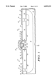
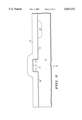
- FIG. 1 is provided to illustrate the features of a graded-channel semiconductor device, a semiconductor device, or a device 10 according to the present invention.
- device 10 is an n-channel IGFET device. This is intended as an example only and as those skilled in the art will appreciate, the present invention applies also to p-channel devices. Alternatively, the structure according to the present invention applies to complementary p-channel/n-channel configurations as well.
- Device 10 is a semiconductor device formed in a semiconductor substrate 11 and comprises a gate structure 20. Gate structure 20 is used to modulate a channel 25 between a source region 43 and a drain region 44. A significant feature of device 10 is that source region 43 and drain region 44 are formed in a body of semiconductor material that is arranged as a pedestal 12 as shown in FIG. 1. Because portions of device 10 are formed in pedestal 12, many of the electrical characteristics of device 10 are improved. For example, the physical isolation provided to device 10 by pedestal 12 reduces the effects of leakage currents and voltage potentials that may be present in the underlying substrate 11. As a result, the breakdown voltage is significantly improved and the effects of parasitic bipolar structures are significantly reduced.
- Device 10 also has a doped region 18, which is used to improve the punch-through resistance between source region 43 and drain region 44.
- Doped region 18 is formed below a major surface 14 of pedestal 12 and doped region 18 has a varying dopant concentration throughout as described below to maximize the ability of doped region 18 to prevent punch-through and adjust the threshold voltage of device 10.
- device 10 further comprises a buried interconnect region 19, a plug contact 21, and a plug contact 22.
- These structures are used as part of an optional interconnect structure to provide electrical connections for device 10 or neighboring device structures (not shown).
- the interconnect structure can also be used to electrically couple voltages to substrate 11 or to various doped regions formed in substrate 11. A further description of the interconnect structure and its applications will be provided shortly.
- Device 10 includes a semiconductor substrate, a body of semiconductor material, or substrate 11, which comprises a semiconductor layer, a diffused well, a substrate region, an epitaxial region on a substrate, or the like.
- substrate 11 typically comprises a lightly doped epitaxial layer on a heavily doped substrate.
- Methods for forming substrate 11 are well known.
- Source region 43 and drain region 44 that extend from major surface 14 to a depth of about 0.1 microns to about 0.3 microns.
- Source region 43 and drain region 44 are n-type conductivity regions having a surface concentration on the order of 1.0 ⁇ 10 20 atoms/cm 3 .
- Source region 43 and drain region 44 are, for example, spaced apart a distance in a range from about 0.25 microns to 0.5 microns. As photolithographic techniques evolve to economically produce smaller dimensions, this distance is scaleable according to classic metal-oxide semiconductor (MOS) scaling techniques.
- MOS metal-oxide semiconductor
- Gate structure 20 of device 10 is formed adjacent to channel region 25 and includes, for example, a region of conductive material 38 electrically insulated from channel region 25 by gate dielectric layer 39.
- Gate dielectric layer 39 preferably comprises an oxide and has a thickness in a range from about 30 angstroms to about 100 angstroms.
- a voltage potential is placed on conductive material 38 using a gate electrode 70.
- Gate electrode 70 is formed from a conductive material, which improves the electrical characteristics of conductive material 38.
- a portion of conductive material 38 overlaps at least a portion of the junction formed by source region 43 and pedestal 12 and at least a portion of the junction formed by drain region 44 and pedestal 12.
- gate control of gate structure 20 is effective across channel region 25. This also significantly enhances device reliability and manufacturability. Insufficient overlap results in erratic manufacturing yields and degrades device performance.
- Gate structure 20 also includes a second thermal oxide layer 34 and first spacers 37, which are used to provide physical and electrical isolation between gate electrode 70 and electrodes 71 and 72. Electrodes 71 and 72 are electrically coupled to source region 43 and drain region 44 respectively. In addition, FIG. 1 illustrates the use of second spacers 47, which may be optionally formed to provide further isolation between gate electrode 70 and electrodes 71 and 72.
- a doped region 18 is formed in channel region 25 and is vertically spaced apart from (i.e., it does not directly contact) major surface 14. Additionally, doped region 18 is both vertically and laterally spaced apart from source region 43 and drain region 44. Further, the lateral extension of doped region 18 is defined independently of the distance between source region 43 and drain region 44.
- Doped region 18 is of the same conductivity type as pedestal 12, but has a higher dopant concentration. Additionally, doped region 18 extends into pedestal 12 to a depth greater than about 0.3 microns. Preferably, doped region 18 is a region having a dopant concentration greater than or equal to approximately 3.0 ⁇ 10 17 atoms/cm 3 (i.e., doped region 18 preferably has a dopant concentration at least an order magnitude greater than the background concentration of pedestal 12 and substrate 11).
- source region 43 and drain region 44 are self-aligned to doped region 18 in order to provide bi-directional device operation (i.e., doped region 18 is substantially centrally located between source region 43 and drain region 44).
- doped region 18 is at least 125 angstroms below major surface 14 with a distance of about 800 angstroms preferred. According to the present invention, the distance that doped region 18 is spaced from major surface 14 contributes to establishing the threshold voltage of graded-channel semiconductor device 10.
- Doped region 18 provides a localized area of charge that functions, among other things, to enhance punch-through resistance. Also, because doped region 18 is spaced apart from source region 43 and drain region 44, device 10 exhibits improved breakdown voltage characteristics, improved switching speeds due to reduced junction capacitance, and improved resistance to hot-carrier injection effects compared to prior art structures where the center doped region contacts the source and drain region. Additionally, because doped region 18 is spaced apart from major surface 14, device 10 exhibits a lower threshold voltage and improved drive capability (i.e., higher transconductance) compared to prior art structures having substantially constant channel doping in the center of the channel that extends all the way to the surface (i.e., extends completely to the surface of the channel region).
- doped region 18 and thickness of gate dielectric layer 39 can be varied to produce devices with various characteristics. For example, with doped region 18 spaced a distance of about 1,125 angstroms from major surface 14 and with gate dielectric layer 39 having a thickness of about 90 angstroms, device 10 exhibits a leakage current (Idss) on the order of 40 nano-amps/micron (at a Vds of 1.8 volts), a threshold voltage on the order of 165 millivolts, a peak transconductance on the order of 65 Siemens/meter, a drive current (Idsat) on the order of 790 micro-amps/micron (at a Vds of 3.3 volts), 555 micro-amps/micron (at a Vds of 2.5 volts), and a breakdown voltage (BVdss) on the order of 7.5 volts.
- Idss leakage current
- Idsat drive current
- BVdss breakdown voltage
- graded-channel device 10 exhibits an Idss on the order of 1.0 nano-amp/micron (at a Vds of 1.8 volts), a threshold voltage on the order of 300 millivolts, a peak transconductance on the order of 60 Siemens/meter, an Idsat on the order of 730 micro-amps/micron (at a Vds of 3.3 volts), an Idsat on the order of 500 micro-amps/micron (at a Vds of 2.5), and a BVdss on the order of 8.0 volts.
- graded-channel device 10 exhibits an Idss on the order of 1.0 pico-amp/micron (at a Vds of 1.8 volts), a threshold voltage on the order of 575 millivolts, a peak transconductance on the order of 53 Siemens/meter, an Idsat on the order of 620 micro-amps (at a Vds of 3.3 volts), an Idsat on the order of 400 micro-amps/micron (at a Vds of 2.5 volts), and a BVdss on the order of 8.25 volts. All of the above examples are drawn with dimensions such that the width of gate structure 20 is about 0.5 microns.
- comparable prior art structures having a 0.5 micron drawn gate dimension and a 90 angstrom gate oxide typically exhibit Idsat values on the order of 400 micro-amps/micron at 3.3 volts and an Idss of about 1.0 nano-amp/micron.
- Comparable prior art structures having a 0.35 micron drawn gate length and a 90 angstrom gate oxide typically exhibit Idsat values on the order of 450 micro-amps/micron at 2.5 volts and an Idss of about 1.0 nano-amp/micron.
- device 10 featuring 1.0 nano-amp/micron Idss capability also shows a significant improvement in Idsat compared to the prior art structures.
- First dielectric layer 24 is used to provide electrical and physical isolation between various elements of FIG. 1. For example, first dielectric layer 24 electrically isolates source region 43 and drain region 44 from any neighboring device structures. The electrical isolation provided by first dielectric layer 24 is comparable to the use of field oxide structures in conventional MOS devices. First dielectric layer 24 is also used to provide electrical isolation as part of the interconnect structure of the present invention as will become more apparent with the description to follow.
- Plug contact 21 comprises a plug region 73, which is used to provide electrical coupling between well region 15 and a contact electrode 75.
- Plug contact 22 also comprises a plug region 73, which is used to electrically couple buried interconnect region 19 to a contact electrode 76. It should also be understood that plug contacts 21 or 22 could also be used to electrically couple a contact electrode (not shown) to substrate 11 and that plug contacts 21 and 22 are used to pass voltage levels or electronic signals through a first dielectric layer 24.
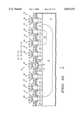
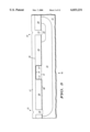
- FIGS. 2-8 a preferred method for forming device 10 is described.
- FIG. 2 illustrates an enlarged cross-sectional view of substrate 11 at an early stage of processing.
- the upper portion of substrate 11 is preferably a lightly doped p-type body of silicon and may be formed by a lightly doped p-type layer on a heavily doped p-type substrate.
- the formation of device 10 begins with the formation of pedestal 12.
- a first masking layer (not shown) is patterned on substrate 11, which acts as a hard mask to define pedestal 12.
- the first masking layer is a 800 angstrom to 2,000 angstrom thick film of silicon dioxide that is grown on substrate 11 and patterned using a photolithographic process.
- a timed reactive ion etch (RIE) is used to remove the portions of substrate 11 that are not covered by the first masking layer.
- Pedestal 12 is the remaining raised portion of substrate 11 that is covered by the first masking layer.
- Pedestal 12 is elevated about 3,000 angstroms to 10,000 angstroms above a surface 80 of substrate 11 and is about 5,000 angstroms to 30,000 angstroms wide.
- the width of pedestal 12 is defined as the distance between the sides 13 of pedestal 12 as shown in FIG. 2.
- Pedestal 12 further comprises a major surface 14 on which portions of device 10 will be formed.
- a first thermal oxide layer 16 with a thickness of about 100 angstroms to 500 angstroms is grown on surface 80, sides 13, and major surface 14.
- a photolithographic masking step, an implant step, and an anneal step can be performed to form the optional buried interconnect region 19 as shown in FIG. 2.
- An arsenic implant dose on the order of 1.0 ⁇ 10 15 atoms/cm 2 to 1.0 ⁇ 10 16 atoms/cm 2 and an implant energy on the order of 80 keV is suitable for forming buried interconnect region 19.
- first dielectric layer 24 is deposited onto surface 80, sides 13, and major surface 14.
- first dielectric layer 24 is deposited using well known deposition techniques (e.g., low pressure chemical vapor deposition (CVD), plasma enhanced CVD, etc.) and comprises a material such as silicon dioxide formed from the decomposition of tetraethylorthosilicate (TEOS).
- CVD low pressure chemical vapor deposition
- TEOS tetraethylorthosilicate
- First dielectric layer 24 is about 4,000 angstroms to 13,000 angstroms thick and should be thick enough to cover sides 13 of pedestal 12.
- first dielectric layer 24 is then planarized to provide a first planar surface 81.
- First dielectric layer 24 can be planarized with either a chemical mechanical polishing (CMP) technique or a photolithographic negative-layer (n-layer) process, both of which are well known.
- CMP chemical mechanical polishing
- n-layer photolithographic negative-layer
- the planarizing process preferably leaves a portion of first dielectric layer 24 and first thermal oxide layer 16 on major surface 14 of pedestal 12. It should also be understood that all of first dielectric layer 24 and first thermal oxide layer 16 can be removed from major surface 14 during the planarizing process.
- Well region 15 is then formed by implanting substrate 11 through first planar surface 81 and is used to prevent the electrical inversion of surface 80 between device 10 and possible surrounding devices not shown.
- a boron implant dose on the order of 1.0 ⁇ 10 12 atoms/cm 2 to 1.0 ⁇ 10 13 atoms/cm 2 and an implant energy on the order of 60 keV is suitable for forming well region 15.
- openings may be optionally formed in first dielectric layer 24 for the formation of plug contacts 21 and 22.
- the formation of the interconnect structure is not required for the formation of device 10.
- a photolithographic masking pattern (not shown) is used to expose the portions of first dielectric layer 24 where plug contacts 21 and 22 are formed.
- An RIE etch is then use to remove the exposed portions of first dielectric layer 24 and expose portions of the underlying well region 15 and buried interconnect region 19.
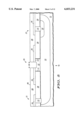
- a first coupling layer 17 is then formed on first planar surface 81 and in the openings of plug contacts 21 and 22 as shown in FIG. 3.
- First coupling layer 17 is made from a conductive material and is used primarily to form plug regions 73. Plug regions 73 are used in plug contacts 21 and 22 to electrically couple to well region 15 and buried interconnect region 19 respectively.
- First coupling layer 17 can comprise a variety of conductive materials such as polysilicon, doped silicon, tungsten, cobalt, chromium, or the like. Such materials can be deposited using a CVD process, a plasma enhanced chemical vapor deposition (PECVD) process, or by a sputtering process.
- PECVD plasma enhanced chemical vapor deposition
- first coupling layer 17 on first planar surface 81 and over major surface 14 have been removed with either an etch or a CMP process. This will electrically isolate each of plug regions 73 from each other. Any remaining portions of first dielectric layer 24 or first thermal oxide layer 16 on major surface 14 of pedestal 12 are then removed.
- a first polysilicon layer 26 is then deposited onto major surface 14 and first planar surface 81. First polysilicon layer 26 is about 500 angstroms to 2,000 angstroms thick and is in direct physical contact with the silicon material of pedestal 12. First polysilicon layer 26 is also in contact with plug regions 73 of plug contacts 21 and 22.
- a photolithographic masking pattern (not shown) and an RIE etch process are used to remove portions of first polysilicon layer 26 to electrically isolate the portion of first polysilicon layer 26 over pedestal 12 from the portions of first polysilicon layer 26 over plug regions 73. This electrical isolation is shown in FIG. 4 as openings 27. After the formation of openings 27, the photolithographic mask is removed to allow further processing.
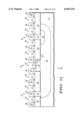
- FIG. 5 illustrates substrate 11 at a subsequent step of manufacture.
- FIG. 5 shows substrate 11 with a second dielectric layer 28 formed on first polysilicon layer 26 and the exposed portions of first dielectric layer 24.
- second dielectric layer 28 is a 4,000 angstrom to 7,000 angstrom thick layer of silicon oxide that is formed from a CVD deposition process.
- a second planar surface 85 is then formed on second dielectric layer 28 using a CMP process.
- Second planar surface 85 of second dielectric layer 28 is then patterned with a photolithographic pattern (not shown) to form a gate opening 29, which has, for example, a width 30 on the order of 0.4 microns to 0.6 microns.
- gate opening 29 is 0.5 microns wide. This establishes a drawn gate dimension. Techniques for forming gate opening 29 are well known in the art. As stated above, as photolithographic capabilities evolve to economically produce smaller dimensions, width 30 is scaleable using classic MOS scaling techniques.
- a reactive ion etch is used to remove the exposed portions of second dielectric layer 28 and first polysilicon layer 26.
- the RIE etch process includes a timed over etch so that a portion of pedestal 12 at major surface 14 is also removed. It should also be understood that the RIE etch process can be modified so that a thin portion of first polysilicon layer 26 is left in gate opening 29 so no part of pedestal 12 is removed.
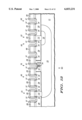
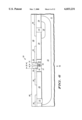
- FIG. 6 illustrates device 10 at a subsequent step of manufacture.
- FIG. 6 shows substrate 11 after second thermal oxide 34 has been formed on the exposed portions of first polysilicon layer 26 and major surface 14.
- Second thermal oxide layer 34 is about 100 angstroms to 500 angstroms thick and can be formed by placing substrate 11 into a high temperature, oxidizing ambient.
- Temporary spacers 36 are then formed by depositing a material such as a polysilicon layer (not shown) onto second planar surface 85 and into gate opening 29. The thickness of the polysilicon layer is selected based upon the desired width of each temporary spacer 36 and thus a desired aperture width 31 to subsequently form doped region 18 (see FIG. 1).
- the polysilicon layer has a thickness of about 1,750 angstroms. This is based on the well known relationship that aperture width 31 is approximately equal to width 30 minus two times the thickness of the polysilicon layer.
- the layer is anisotropically etched to form temporary spacers 36 as shown in FIG. 6.
- the anisotropic etch removes the portions of the polysilicon layer on major surface 14 and provides aperture width 31.
- the polysilicon layer is etched using, for example, well known reactive ion etching (RIE) techniques.
- Temporary spacers 36 provide the sub-photolithographic aspect of doped region 18. Alternatively, temporary spacers could be formed using silicon nitride.
- doped region 18 is formed preferably using ion implantation and annealing techniques.
- doped region 18 preferably is formed by a series of ion implants including, a first boron implant dose of about 7.0 ⁇ 10 12 atoms/cm 2 at an energy of about 80 keV (represented by region 35), a second boron implant dose of about 7.0 ⁇ 10 12 atoms/cm 2 at 40 keV (represented by region 33), and a third boron implant dose of about 4.0 ⁇ 10 11 atoms/cm 2 at an energy of about 10 keV (represented by region 32).
- the first and second boron implant are the same as above, but the third boron implant dose is on the order of about 3.0 ⁇ 10 12 atoms/cm 2 at an energy of about 10 keV.
- the first boron implant is the same as above, but the second boron implant is on the order of 7.0 ⁇ 10 12 atoms/cm 2 at 50 kev and the third boron implant is not done (i.e., region 32 is not formed).
- the implant energy is selected for doping regions 32, 33, and 35 so that once regions 32, 33, and 35 are annealed to form doped region 18, doped region 18 is spaced a distance from major surface 14 on the order of at least 125 angstroms.
- first spacers 37 are removed using well known techniques.
- a layer of silicon nitride (not shown) is deposited onto second planar surface 85 and into gate opening 29.
- the layer of silicon nitride is also formed on second thermal oxide layer 34 overlying major surface 14.
- the layer of silicon nitride is anisotropically etched to form first spacers 37 as shown in FIG. 7.
- the anisotropic etch removes the layer of silicon nitride on second thermal oxide layer 34 over major surface 14.
- a wet etch is then used to remove the portions of second thermal oxide layer 34 that were exposed by the anisotropic etch used to form first spacers 37.
- the wet etch leaves portions of second thermal oxide layer 34 between first spacers 37 and first polysilicon layer 26 on pedestal 12.
- the wet etch can also remove a portion of pedestal 12 to clean major surface 14 for subsequent processing.
- gate dielectric layer 39 is then formed as shown in FIG. 7.
- gate dielectric layer 39 comprises a thermal oxide and has a thickness on the order of about 30 angstroms to about 100 angstroms (90 angstroms was used for the examples provided above).
- regions 32, 33 and 35 are annealed to activate the implanted dopant to form doped region 18.
- a layer of conductive material 38 is formed over major surface 14, second planar surface 85, and into gate opening 29.
- Conductive layer 38 preferably comprises polysilicon or amorphous silicon and in this example, has a thickness on the order of 4,000 angstroms. This thickness varies depending on width 30 of gate opening 39. Methods for forming layer 38 are well known. It should also be understood that the gate structure of device 10 can be formed from other materials used in the semiconductor industry such as cobalt, tungsten, molybdenum, or the like.
- FIG. 8 illustrates device 10 at a subsequent step in manufacture.
- FIG. 8 shows substrate 11 after layer 38 has been planarized.
- layer 38 is planarized using chemical mechanical polishing (CMP) techniques, which are well known.
- CMP chemical mechanical polishing
- a portion of layer 38 remains in gate opening 29 and becomes a portion of gate structure 20 (see FIG. 1).
- the portion of layer 38 that remains in gate opening 29 typically has a thickness on the order of 3,500 angstroms to 6,000 angstroms.
- portions of second dielectric layer 28 are removed using, for example, conventional wet etching techniques to form the structure shown in FIG. 8.
- the portion of second dielectric layer 28 overlying gate structure 20 and first polysilicon layer 26 is removed.
- a portion of second dielectric layer 28 may be left in openings 27 as shown in FIG. 8.
- a third dielectric layer 40 is then formed on the exposed surfaces of gate structure 20 and first layer of polysilicon 26.
- third dielectric layer 40 is about 100 angstroms to 500 angstroms thick and is formed from the chemical vapor deposition of silicon dioxide.
- Third dielectric layer 40 is used as a screen oxide for the subsequent implant steps used to form a first doped region 41 and a second doped region 42.
- First doped region 41 is formed with a n-type dopant (e.g., phosphorous) that is ion implanted into first polysilicon layer 26 and is performed to enhance the electrical characteristics of first polysilicon layer 26.
- Second doped region 42 is formed such that a portion of the dopant extends below major surface 14 into pedestal 12, which is used to form source region 43 and drain region 44 (see FIG. 1). Note that a portion of second doped region 42 also extends into plug regions 73, which only further serves to enhance the electrical characteristics of plug contacts 21 and 22. It should also be understood that the conductivity of plug contacts 21 and 22 could be doped to be of opposite conductivity if p-channel devices (not shown) are formed on semiconductor substrate 11.
- first doped region 41 and a second doped region 42 in first polysilicon layer 26 are shown. It should be understood that dopant will also enter portions of first dielectric layer 28.
- a key feature of the implantation steps is that these steps are self-aligned to gate structure 20. This allows gate structure 20 to overlap source region 43 and drain region 44 after first doped region 41 and a second doped region 42 have been annealed (as described below). This adds to device reliability and greatly enhances manufacturability. Additionally, this eliminates the need for source and drain extensions, which add processing steps and degrade device performance.
- An implant dose on the order of 1.0 ⁇ 10 15 atoms/cm 2 to 1.0 ⁇ 10 16 atoms/cm 2 and an implant energy on the order of 60 keV is suitable for forming first doped region 41.
- An implant dose on the order of 1.0 ⁇ 10 15 atoms/cm 2 to 1.0 ⁇ 10 16 atoms/cm 2 and an implant energy on the order of 160 keV is suitable for forming second doped region 42.
- the dopant from the implantation step used to form second doped region 42 extends into pedestal 12 and is used to form source region 43 and drain region 44.
- the implanted dopant of first doped region 41 and a second doped region 42 is activated using conventional rapid thermal anneal techniques to form source region 43 and drain region 44 as shown in FIG. 1.
- source region 43 and drain region 44 are formed so they are elevated above first surface 80 of substrate 11.
- An anneal of about 40 seconds at about 1050° C. is suitable.
- an equivalent furnace anneal is used.
- doped region 18 has a width of less than 0.3 microns, with a width on the order of 0.15 micron to about 0.25 micron being typical.
- Third dielectric layer 40 is removed using a conventional wet etch process.
- a spacer layer (not shown) is deposited onto gate structure 20, first polysilicon layer 26, and first dielectric layer 28 followed by a conventional reactive ion etch to form second spacers 47 as shown in FIG. 1.
- the spacer layer preferably comprises silicon nitride, and the use of second spacers 47 is optional and can be used in the formation of source electrode 71, drain electrode 72, and gate electrode 70.
- source electrode 71, drain electrode 72, and gate electrode 70 are formed using, for example, conventional self-aligned silicide techniques.
- source electrode 71, drain electrode 72, and gate electrode 70 have a conductive layer 46 that is formed on all exposed surfaces of first polysilicon layer 26 and second polysilicon layer 38.
- Conductive layer 46 is formed to enhance the electrical properties of first polysilicon layer 26 and second polysilicon layer 38 and comprises titanium silicide, cobalt silicide, or the like.
- the above method provides a self-aligned graded-channel device 10 having sub-photolithographic features. This provides a graded-channel device having bi-directional high performance characteristics with an enhanced punch-through resistance.
- FIG. 9 illustrates an alternate configuration of a device according to the present invention.
- FIG. 9 shows a dual gate n-channel device 50 embodying many of the elements of the present invention.
- Dual gate n-channel device 50 is formed by two semiconductor devices, designated by gate structure 20 and gate structure 59, which are formed in the same pedestal 12.
- the device of gate structure 20 has a source region 43, a drain region 44, and a doped region 18 all described above and shown in FIG. 1.
- the device of gate structure 59 is an additional device that is formed in conjunction with device 10 and uses a portion of drain region 44 as its source and has its own drain region 51.
- Gate structure 20 and gate structure 59 act as the two input terminals of dual gate n-channel device 50, and dual gate n-channel device 50 is formed using the same process as described above.
- the present invention also provides for an interconnect structure or interconnect methodology that can be used to provide electrical connections within semiconductor devices and between neighboring semiconductor device structures.
- a significant feature of the interconnect structure is that it forms electrical connections at a finer pitch than is possible with conventional photolithographic techniques.
- An additional benefit of the interconnect structure of the present invention is that it is easily integrated into the process flow to form device 10 described above. In the following description, an alternate method for forming device 10 is provided to further simplify the integration of the formation of an interconnect structure into the process used to form device 10.
- Interconnect structure 90 includes, in this embodiment, a semiconductor device such as device 10 or 50 described above. It should also be understood that the elements of interconnect structure 90 can be used with many conventional semiconductor devices having a structure different than device 10 or 50. Interconnect structure 90 comprises two conductive layers, a first conductor 60 and a second conductor 97, that are used to transport electrical signals or voltage potentials to neighboring devices structures (not shown). In FIG. 10, first conductor 60 and second conductor 97 are shown in a repeating pattern across interconnect structure 90 to demonstrate the high packing density or small pitch of the present invention.
- first conductor 60 comprises a conductive layer 96 formed on second polysilicon layer 38.
- second polysilicon layer 38 is used to form part of first conductor 60. This is shown to demonstrate how interconnect structure 90 can be integrated into the formation of gate structure 20 of device 10. It should be understood that first conductor 60 can be formed from a single layer of conductive material and that the use of conductive layer 96 is optional.
- Second conductor 97 comprises a conductive layer 95 formed on first polysilicon layer 26.
- first polysilicon layer 26 is used to form part of second conductor 97. This is shown to demonstrate how interconnect structure 90 can be integrated into the formation of device 10. It should be understood that second conductor 97 can be formed from a single layer of conductive material and that the use of conductive layer 95 is optional.
- Conductive layers 95 and 96 preferably comprise a metallic compound made from materials such as cobalt, chromium, molybdenum, or titanium.
- First conductor 60 is preferably formed from a layer of polysilicon that is physically isolated from second conductor 97 by first spacers 37.
- First spacers 37 can be the same spacers used to define gate structure 20 in FIG. 1. This simplifies the processing steps necessary to form interconnect structure 90.
- First spacers 37 have an interior side, which is defined as the side that physically contacts second polysilicon layer 38.
- First spacers 37 also have an exterior side, which is defined as the portions of first spacers 37 that contact second conductor 97.
- first conductor 60 has a width 61 that is defined as the distance separating the interior side of first spacers 37.
- Second conductor 97 has a width 62 that is defined as the width of the exterior side of first spacers 37 minus the portion of first polysilicon layer 26 that is lost due to the formation of second thermal oxide layer 34. Therefore, the effective pitch of the present invention is width 63, which is the sum of width 61 and the width of one first spacer 37.
- the effective pitch of interconnect structure 90 can also be defined as the width of one of first spacers 37 and the thickness of second thermal layer 34, plus the average width of first conductor 60 and second conductor 97.
- the pitch of an interconnect layer refers to the width of the interconnect layer plus the width of the space between neighboring lines of the interconnect layer.
- a conventional photolithographic process that has a minimum feature size of 0.5 ⁇ m is limited to a pitch of 1.0 ⁇ m (i.e., 0.5 ⁇ m for the interconnect layer and 0.5 ⁇ m for the space to isolate the interconnect layer).
- interconnect structure 90 of the present invention are not limited by the photolithographic process and offer a much improved pitch versus conventional processes. Since first conductor 60 and second conductor 97 are self-aligned and separated by at least one spacer, there is no need to rely on the photolithographic process to physically isolate conductors 60 and 97. For example, if a photolithographic process with a minimum geometry capability of 0.5 ⁇ m is used to form interconnect structure 90, then the pitch of the structure is approximately 0.5 ⁇ m (i.e., 0.4 ⁇ m for either width 61 of first conductor 60 or width 62 of second conductor 97, and approximately 0.1 ⁇ m for spacer 37). Therefore, the average pitch of interconnect structure 90 is substantially equal to the capability of the photolithographic process used to define interconnect structure 90.
- interconnect structure 90 in conjunction with device 10 of the previous narration will be provided. This is done to avoid unnecessary repetition, but it should also be understood that interconnect structure 90 can be formed independently of device 10. Pedestal 12, buried interconnect region 19, first thermal oxide layer 16, plug regions 73, and first dielectric layer 24 are formed in a similar fashion as provided above for device 10. Second conductors 97 are formed in a slightly different manner than in the method described above. First polysilicon layer 26 is deposited onto substrate 11 followed by the deposition of second dielectric layer 28. Previously, first polysilicon layer 26 was patterned and etched before the formation of second dielectric layer 28.
- Second dielectric layer 28 is then planarized using a CMP process to provide second planar surface 85. Following the planarization process, second dielectric layer 28 is then patterned using a photolithographic mask (not shown). A reactive ion etch is then used to remove portions of second dielectric layer 28 and first polysilicon layer 26 to form openings 65 as shown in FIG. 11. Openings 65 provide the physical and electrical isolation in first polysilicon layer 26 to define the regions of second conductor 97. Therefore, each of second conductors 97 shown in FIG. 10 is electrically isolated from each other and each can be used to transport a different electrical signal or voltage potential.
- gate opening 29 is formed to expose a portion of pedestal 12. Note, no additional process steps are required to form gate opening 29.
- the photolithographic mask is then removed and the exposed portions of pedestal 12 and first polysilicon layer 26 are oxidized to form second thermal oxide layer 34. Since first polysilicon layer 26 is an electrically conductive layer, second thermal oxide layer 34 provides part of the necessary electrical isolation between first conductors 60 and second conductors 97. It is necessary to electrically isolate second conductors 97 from the subsequent structures formed in openings 65 as described below.
- first conductors 60 in openings 65 will be provided.
- a layer of silicon nitride (not shown) is deposited onto substrate 11 and into openings 65 and anisotropically etched to form first spacers 37.
- First spacers 37 will have a width that is approximately equal to the thickness of the silicon nitride layer from which first spacers 37 are formed.
- the process to form first spacers 37 is the same as the process described above in the formation of device 10.
- a portion of second thermal oxide layer 34 on pedestal 12 is removed and gate dielectric layer 39 is grown on major surface 14 of pedestal 12.
- a third polysilicon layer 66 is conformally deposited onto substrate 11 and onto gate dielectric layer 39.
- Third polysilicon layer 66 is about 300 angstroms to 1,000 angstroms thick and is formed for the following implantation steps used to form doped region 18 (see FIG. 1). Additionally, a screen oxide (not shown) is thermally grown onto third polysilicon layer 66 and is about 50 angstroms to 300 angstroms thick. A sequence of implantation steps, such as the ones provided above, can be used to form doping region 32, 33, 35.
- a wet etch process is then used to remove the screen oxide layer and expose the underlying third polysilicon layer 66. It should be understood that the process steps used in the formation of gate dielectric layer 39 or doping regions 32, 33, and 35 are not a necessary requirement for the formation of interconnect structure 90. It is possible to use interconnect structure 90 for other device structures so that the processing steps particular to device 10 should be considered optional.
- the method for forming interconnect structure 90 also provides a slightly different method of forming portions of device 10. As described earlier, doping regions 32, 33, and 35 are formed by implanting pedestal 12 through an aperture, the aperture being provided by spacers 36 made from polysilicon. In this alternate method, doping regions 32, 33, and 35 are formed by implanting pedestal 12 through an aperture provided by first spacers 37, third polysilicon layer 66, and the screen oxide layer.
- a conductive material is deposited onto third polysilicon layer 66 to provide the material used to form first conductor 60.
- second polysilicon layer 38 can be deposited to fill openings 65. This step is already provided in the method to form device 10 as second polysilicon layer 38 was used to fill gate opening 29. After deposition, either a CMP or an anisotropic etch process is used to remove the portions of second polysilicon layer 38 on second planar surface 85. This step physically and electrically isolates portions of second polysilicon layer 38 to form first conductors 60. It should also be understood that openings 65 and gate opening 29 can be filled with a variety of conductive materials such as polysilicon, amorphous silicon, tungsten, cobalt, chromium, or the like.
- each of first conductors 60 is electrically isolated from each other and is electrically isolated from second conductors 97.
- second conductors 97 can be used to electrically couple to plug regions 73 in the formation of plug contacts 21 and 22. It should also be understood that first conductors 60 and second conductors 97 can be used to carry electrical signals throughout an integrated circuit (not shown) and do not necessarily have to be coupled to portions of device 10 such as plug contacts 21 and 22 or gate structure 20.
- first conductors 60 and second conductors 97 may be optionally formed on first conductors 60 and second conductors 97 respectively.
- Conductive layers 95 and 96 are preferably formed from a silicidation process to form a metal compound comprising titanium, cobalt, or similar material.
- First spacers 37 provide an additional benefit in that they can be used in the silicidation process to electrically isolate first conductors 60 and second conductors 97.
- First spacers 37 are preferably made from silicon nitride and thus the metal compound used to form conductive layers 95 and 96 will not form along the surface of first spacers 37.
- the present invention provides a graded-channel semiconductor device and an interconnect structure.
- the present invention also provides a method for forming both structures together or forming each structure separately.
- the graded-channel semiconductor device of the present invention offers many advantages over conventional semiconductor devices such as improved punch-through resistance, improved current densities at lower operating voltages, and improved manufacturability.
- the interconnect structure of the present invention offers advantages such as an improved pitch width, which in turn increase the density of interconnect layers in the structure. These advantages provide for a device that has improved functionality with a lower manufacturing cost.
Abstract
Description
Claims (20)
Priority Applications (1)
| Application Number | Priority Date | Filing Date | Title |
|---|---|---|---|
| US09/121,812 US6033231A (en) | 1996-02-29 | 1998-07-24 | Semiconductor device having a pedestal and method of forming |
Applications Claiming Priority (2)
| Application Number | Priority Date | Filing Date | Title |
|---|---|---|---|
| US08/608,864 US5818098A (en) | 1996-02-29 | 1996-02-29 | Semiconductor device having a pedestal |
| US09/121,812 US6033231A (en) | 1996-02-29 | 1998-07-24 | Semiconductor device having a pedestal and method of forming |
Related Parent Applications (1)
| Application Number | Title | Priority Date | Filing Date |
|---|---|---|---|
| US08/608,864 Division US5818098A (en) | 1996-02-29 | 1996-02-29 | Semiconductor device having a pedestal |
Publications (1)
| Publication Number | Publication Date |
|---|---|
| US6033231A true US6033231A (en) | 2000-03-07 |
Family
ID=24438366
Family Applications (2)
| Application Number | Title | Priority Date | Filing Date |
|---|---|---|---|
| US08/608,864 Expired - Fee Related US5818098A (en) | 1996-02-29 | 1996-02-29 | Semiconductor device having a pedestal |
| US09/121,812 Expired - Fee Related US6033231A (en) | 1996-02-29 | 1998-07-24 | Semiconductor device having a pedestal and method of forming |
Family Applications Before (1)
| Application Number | Title | Priority Date | Filing Date |
|---|---|---|---|
| US08/608,864 Expired - Fee Related US5818098A (en) | 1996-02-29 | 1996-02-29 | Semiconductor device having a pedestal |
Country Status (1)
| Country | Link |
|---|---|
| US (2) | US5818098A (en) |
Cited By (4)
| Publication number | Priority date | Publication date | Assignee | Title |
|---|---|---|---|---|
| US20040004264A1 (en) * | 2002-07-04 | 2004-01-08 | Samsung Electronics Co., Ltd. | Semiconductor device and method of manufacturing the same |
| GB2397693A (en) * | 2002-07-04 | 2004-07-28 | Samsung Electronics Co Ltd | Semiconductor device and method of manufacture |
| US20070090434A1 (en) * | 2004-01-10 | 2007-04-26 | Hvvi Semiconductors, Inc. | Power semiconductor device and method therefor |
| US8530963B2 (en) | 2005-01-06 | 2013-09-10 | Estivation Properties Llc | Power semiconductor device and method therefor |
Families Citing this family (10)
| Publication number | Priority date | Publication date | Assignee | Title |
|---|---|---|---|---|
| US5818098A (en) * | 1996-02-29 | 1998-10-06 | Motorola, Inc. | Semiconductor device having a pedestal |
| US6303448B1 (en) * | 1998-11-05 | 2001-10-16 | Taiwan Semiconductor Manufacturing Company | Method for fabricating raised source/drain structures |
| US6058023A (en) * | 1998-11-06 | 2000-05-02 | Hughes Electronics Corporation | Isolation of high-voltage components in a dense environment |
| US6555437B1 (en) * | 2001-04-27 | 2003-04-29 | Advanced Micro Devices, Inc. | Multiple halo implant in a MOSFET with raised source/drain structure |
| US6452236B1 (en) * | 2001-05-31 | 2002-09-17 | Texas Instruments, Incorporated | Channel implant for improving NMOS ESD robustness |
| TW502453B (en) * | 2001-09-06 | 2002-09-11 | Winbond Electronics Corp | MOSFET and the manufacturing method thereof |
| US8338887B2 (en) * | 2005-07-06 | 2012-12-25 | Infineon Technologies Ag | Buried gate transistor |
| US7300850B2 (en) * | 2005-09-30 | 2007-11-27 | Semiconductor Components Industries, L.L.C. | Method of forming a self-aligned transistor |
| US20110083065A1 (en) * | 2009-10-01 | 2011-04-07 | Telefonaktiebolaget L M Ericsson (Publ) | False Detection Reduction in Communication Systems |
| EP4290585A1 (en) * | 2022-06-08 | 2023-12-13 | Nexperia B.V. | Lateral oriented metal-oxide-semiconductor, mos device comprising a semiconductor body |
Citations (14)
| Publication number | Priority date | Publication date | Assignee | Title |
|---|---|---|---|---|
| US4198252A (en) * | 1978-04-06 | 1980-04-15 | Rca Corporation | MNOS memory device |
| US4371955A (en) * | 1979-02-22 | 1983-02-01 | Fujitsu Limited | Charge-pumping MOS FET memory device |
| US4697198A (en) * | 1984-08-22 | 1987-09-29 | Hitachi, Ltd. | MOSFET which reduces the short-channel effect |
| US4706378A (en) * | 1985-01-30 | 1987-11-17 | Texas Instruments Incorporated | Method of making vertical bipolar transistor having base above buried nitride dielectric formed by deep implantation |
| US4857476A (en) * | 1988-01-26 | 1989-08-15 | Hewlett-Packard Company | Bipolar transistor process using sidewall spacer for aligning base insert |
| US5021845A (en) * | 1985-08-30 | 1991-06-04 | Texas Instruments Incorporated | Semiconductor device and process fabrication thereof |
| US5250464A (en) * | 1992-03-11 | 1993-10-05 | Texas Instruments Incorporated | Method of making a low capacitance, low resistance sidewall antifuse structure |
| US5395773A (en) * | 1994-03-31 | 1995-03-07 | Vlsi Technology, Inc. | MOSFET with gate-penetrating halo implant |
| US5434093A (en) * | 1994-08-10 | 1995-07-18 | Intel Corporation | Inverted spacer transistor |
| US5548154A (en) * | 1991-03-28 | 1996-08-20 | Sgs-Thomson Microelectronics, Inc. | Isoplanar isolated active regions |
| US5600168A (en) * | 1994-04-20 | 1997-02-04 | Lg Semicon Co., Ltd. | Semiconductor element and method for fabricating the same |
| US5661048A (en) * | 1995-03-21 | 1997-08-26 | Motorola, Inc. | Method of making an insulated gate semiconductor device |
| US5696544A (en) * | 1994-04-14 | 1997-12-09 | Canon Kabushiki Kaisha | Ink jet head substrate and ink jet head using same arranged staggeredly |
| US5818098A (en) * | 1996-02-29 | 1998-10-06 | Motorola, Inc. | Semiconductor device having a pedestal |
-
1996
- 1996-02-29 US US08/608,864 patent/US5818098A/en not_active Expired - Fee Related
-
1998
- 1998-07-24 US US09/121,812 patent/US6033231A/en not_active Expired - Fee Related
Patent Citations (14)
| Publication number | Priority date | Publication date | Assignee | Title |
|---|---|---|---|---|
| US4198252A (en) * | 1978-04-06 | 1980-04-15 | Rca Corporation | MNOS memory device |
| US4371955A (en) * | 1979-02-22 | 1983-02-01 | Fujitsu Limited | Charge-pumping MOS FET memory device |
| US4697198A (en) * | 1984-08-22 | 1987-09-29 | Hitachi, Ltd. | MOSFET which reduces the short-channel effect |
| US4706378A (en) * | 1985-01-30 | 1987-11-17 | Texas Instruments Incorporated | Method of making vertical bipolar transistor having base above buried nitride dielectric formed by deep implantation |
| US5021845A (en) * | 1985-08-30 | 1991-06-04 | Texas Instruments Incorporated | Semiconductor device and process fabrication thereof |
| US4857476A (en) * | 1988-01-26 | 1989-08-15 | Hewlett-Packard Company | Bipolar transistor process using sidewall spacer for aligning base insert |
| US5548154A (en) * | 1991-03-28 | 1996-08-20 | Sgs-Thomson Microelectronics, Inc. | Isoplanar isolated active regions |
| US5250464A (en) * | 1992-03-11 | 1993-10-05 | Texas Instruments Incorporated | Method of making a low capacitance, low resistance sidewall antifuse structure |
| US5395773A (en) * | 1994-03-31 | 1995-03-07 | Vlsi Technology, Inc. | MOSFET with gate-penetrating halo implant |
| US5696544A (en) * | 1994-04-14 | 1997-12-09 | Canon Kabushiki Kaisha | Ink jet head substrate and ink jet head using same arranged staggeredly |
| US5600168A (en) * | 1994-04-20 | 1997-02-04 | Lg Semicon Co., Ltd. | Semiconductor element and method for fabricating the same |
| US5434093A (en) * | 1994-08-10 | 1995-07-18 | Intel Corporation | Inverted spacer transistor |
| US5661048A (en) * | 1995-03-21 | 1997-08-26 | Motorola, Inc. | Method of making an insulated gate semiconductor device |
| US5818098A (en) * | 1996-02-29 | 1998-10-06 | Motorola, Inc. | Semiconductor device having a pedestal |
Non-Patent Citations (6)
| Title |
|---|
| H. Lin et al., "Computer Analysis of the Double-Diffused MOS Transistor for Integrated Circuits," Transactions on Electron Devices, vol. Ed-20, No. 3, Mar. 1973, pp. 275-282. |
| H. Lin et al., Computer Analysis of the Double Diffused MOS Transistor for Integrated Circuits, Transactions on Electron Devices, vol. Ed 20, No. 3, Mar. 1973, pp. 275 282. * |
| K. Lee et al., "Room Temperature 0.1 μm CMOS Technology with 11.8 ps Gate Delay," IEEE 1993, Washington, DC, pp. 131-134. |
| K. Lee et al., Room Temperature 0.1 m CMOS Technology with 11.8 ps Gate Delay, IEEE 1993, Washington, DC, pp. 131 134. * |
| S. Shimizu et al., "0.15μm CMOS Process for High Performance and High Reliability," IEEE 1994, San Francisco, CA, pp. 67-70. |
| S. Shimizu et al., 0.15 m CMOS Process for High Performance and High Reliability, IEEE 1994, San Francisco, CA, pp. 67 70. * |
Cited By (19)
| Publication number | Priority date | Publication date | Assignee | Title |
|---|---|---|---|---|
| US7268043B2 (en) | 2002-07-04 | 2007-09-11 | Samsung Electronics Co., Ltd. | Semiconductor device and method of manufacturing the same |
| GB2397693A (en) * | 2002-07-04 | 2004-07-28 | Samsung Electronics Co Ltd | Semiconductor device and method of manufacture |
| GB2397694A (en) * | 2002-07-04 | 2004-07-28 | Samsung Electronics Co Ltd | Semiconductor device and method of manufacture |
| GB2397693B (en) * | 2002-07-04 | 2004-11-17 | Samsung Electronics Co Ltd | Semiconductor device and method of manufacture |
| GB2397694B (en) * | 2002-07-04 | 2004-11-24 | Samsung Electronics Co Ltd | Semiconductor device and method of manufacture |
| US20060008994A1 (en) * | 2002-07-04 | 2006-01-12 | Samsung Electronics Co., Ltd. | Semiconductor device and method of manufacturing the same |
| US7009255B2 (en) | 2002-07-04 | 2006-03-07 | Samsung Electronics Co., Ltd. | Semiconductor device having punch-through structure off-setting the edge of the gate electrodes |
| US20070087500A1 (en) * | 2002-07-04 | 2007-04-19 | Samsung Electronics Co., Ltd. | Semiconductor device and method of manufacturing the same |
| US20040004264A1 (en) * | 2002-07-04 | 2004-01-08 | Samsung Electronics Co., Ltd. | Semiconductor device and method of manufacturing the same |
| US7259069B2 (en) | 2002-07-04 | 2007-08-21 | Samsung Electronics Co., Ltd. | Semiconductor device and method of manufacturing the same |
| US20070090434A1 (en) * | 2004-01-10 | 2007-04-26 | Hvvi Semiconductors, Inc. | Power semiconductor device and method therefor |
| US20100032750A1 (en) * | 2004-01-10 | 2010-02-11 | Hvvi Semiconductors, Inc. | Power Semiconductor Device And Method Therefor |
| US7847369B2 (en) | 2004-01-10 | 2010-12-07 | Hvvi Semiconductors, Inc. | Radio frequency power semiconductor device comprising matrix of cavities as dielectric isolation structure |
| US7898057B2 (en) | 2004-01-10 | 2011-03-01 | Hvvi Semiconductors, Inc. | Radio frequency power semiconductor device package comprising dielectric platform and shielding plate |
| US8471378B2 (en) | 2004-01-10 | 2013-06-25 | Estivation Properties Llc | Power semiconductor device and method therefor |
| US9029946B2 (en) | 2004-01-10 | 2015-05-12 | Estivation Properties Llc | Power semiconductor device and method therefor |
| US9177866B2 (en) | 2004-01-10 | 2015-11-03 | Estivation Properties Llc | Power semiconductor device and method therefor |
| US9865590B2 (en) | 2004-01-10 | 2018-01-09 | Xenogenic Development Limited Liability Company | Power semiconductor device and method therefor |
| US8530963B2 (en) | 2005-01-06 | 2013-09-10 | Estivation Properties Llc | Power semiconductor device and method therefor |
Also Published As
| Publication number | Publication date |
|---|---|
| US5818098A (en) | 1998-10-06 |
Similar Documents
| Publication | Publication Date | Title |
|---|---|---|
| US5712501A (en) | Graded-channel semiconductor device | |
| US6025237A (en) | Methods of forming field effect transistors having graded drain region doping profiles therein | |
| US10134892B2 (en) | High voltage device with low Rdson | |
| US6841834B2 (en) | Doubly asymmetric double gate transistor structure | |
| US5844278A (en) | Semiconductor device having a projecting element region | |
| US9184283B2 (en) | High voltage device | |
| US7417266B1 (en) | MOSFET having a JFET embedded as a body diode | |
| KR100366965B1 (en) | Soi cmos body contact through gate, self-aligned to source-drain diffusions | |
| US5627097A (en) | Method for making CMOS device having reduced parasitic capacitance | |
| US6177299B1 (en) | Transistor having substantially isolated body and method of making the same | |
| US20040126975A1 (en) | Double gate semiconductor device having separate gates | |
| US7446354B2 (en) | Power semiconductor device having improved performance and method | |
| US5382536A (en) | Method of fabricating lateral DMOS structure | |
| US6737710B2 (en) | Transistor structure having silicide source/drain extensions | |
| US5399508A (en) | Method for self-aligned punchthrough implant using an etch-back gate | |
| US10211336B2 (en) | LDMOS transistor structures and integrated circuits including LDMOS transistor structures | |
| KR20060111859A (en) | Semiconductor device having screening electrode and method | |
| EP0603102B1 (en) | Low-temperature MOSFET source drain structure with ultra-short channel | |
| US6033231A (en) | Semiconductor device having a pedestal and method of forming | |
| KR20010092309A (en) | Decoupling capacitors and methods for forming the same | |
| US6388298B1 (en) | Detached drain MOSFET | |
| US6252283B1 (en) | CMOS transistor design for shared N+/P+ electrode with enhanced device performance | |
| US6441434B1 (en) | Semiconductor-on-insulator body-source contact and method | |
| US20050224880A1 (en) | Multi-gate MOS transistor and method of manufacturing the same | |
| US6084269A (en) | Semiconductor device and method of making |
Legal Events
| Date | Code | Title | Description |
|---|---|---|---|
| FPAY | Fee payment |
Year of fee payment: 4 |
|
| AS | Assignment |
Owner name: FREESCALE SEMICONDUCTOR, INC., TEXAS Free format text: ASSIGNMENT OF ASSIGNORS INTEREST;ASSIGNOR:MOTOROLA, INC.;REEL/FRAME:015698/0657 Effective date: 20040404 Owner name: FREESCALE SEMICONDUCTOR, INC.,TEXAS Free format text: ASSIGNMENT OF ASSIGNORS INTEREST;ASSIGNOR:MOTOROLA, INC.;REEL/FRAME:015698/0657 Effective date: 20040404 |
|
| AS | Assignment |
Owner name: CITIBANK, N.A. AS COLLATERAL AGENT, NEW YORK Free format text: SECURITY AGREEMENT;ASSIGNORS:FREESCALE SEMICONDUCTOR, INC.;FREESCALE ACQUISITION CORPORATION;FREESCALE ACQUISITION HOLDINGS CORP.;AND OTHERS;REEL/FRAME:018855/0129 Effective date: 20061201 Owner name: CITIBANK, N.A. AS COLLATERAL AGENT,NEW YORK Free format text: SECURITY AGREEMENT;ASSIGNORS:FREESCALE SEMICONDUCTOR, INC.;FREESCALE ACQUISITION CORPORATION;FREESCALE ACQUISITION HOLDINGS CORP.;AND OTHERS;REEL/FRAME:018855/0129 Effective date: 20061201 |
|
| REMI | Maintenance fee reminder mailed | ||
| AS | Assignment |
Owner name: VENTURE LENDING & LEASING IV, INC AND, CALIFORNIA Free format text: SECURITY AGREEMENT;ASSIGNOR:OPVISTA;REEL/FRAME:019910/0285 Effective date: 20070815 |
|
| LAPS | Lapse for failure to pay maintenance fees | ||
| STCH | Information on status: patent discontinuation |
Free format text: PATENT EXPIRED DUE TO NONPAYMENT OF MAINTENANCE FEES UNDER 37 CFR 1.362 |
|
| FP | Lapsed due to failure to pay maintenance fee |
Effective date: 20080307 |
|
| AS | Assignment |
Owner name: FREESCALE SEMICONDUCTOR, INC., TEXAS Free format text: PATENT RELEASE;ASSIGNOR:CITIBANK, N.A., AS COLLATERAL AGENT;REEL/FRAME:037354/0225 Effective date: 20151207 |