US6033966A - Method for making an 8-shaped storage node DRAM cell - Google Patents

Method for making an 8-shaped storage node DRAM cell Download PDF

Info

Publication number
US6033966A
US6033966A US09/189,066 US18906698A US6033966A US 6033966 A US6033966 A US 6033966A US 18906698 A US18906698 A US 18906698A US 6033966 A US6033966 A US 6033966A
Authority
US
United States
Prior art keywords
storage node
layer
conducting layer
bit line
dielectric layer
Prior art date
Legal status (The legal status is an assumption and is not a legal conclusion. Google has not performed a legal analysis and makes no representation as to the accuracy of the status listed.)
Expired - Fee Related
Application number
US09/189,066
Inventor
Kung Linliu
Current Assignee (The listed assignees may be inaccurate. Google has not performed a legal analysis and makes no representation or warranty as to the accuracy of the list.)
Taiwan Semiconductor Manufacturing Co TSMC Ltd
Original Assignee
Worldwide Semiconductor Manufacturing Corp
Priority date (The priority date is an assumption and is not a legal conclusion. Google has not performed a legal analysis and makes no representation as to the accuracy of the date listed.)
Filing date
Publication date
Application filed by Worldwide Semiconductor Manufacturing Corp filed Critical Worldwide Semiconductor Manufacturing Corp
Priority to US09/189,066 priority Critical patent/US6033966A/en
Assigned to WORLDWIDE SEMICONDUCTOR MANUFACTURING CORPORATION reassignment WORLDWIDE SEMICONDUCTOR MANUFACTURING CORPORATION ASSIGNMENT OF ASSIGNORS INTEREST (SEE DOCUMENT FOR DETAILS). Assignors: LINLIU, KUNG
Priority to TW088106107A priority patent/TW456000B/en
Application granted granted Critical
Publication of US6033966A publication Critical patent/US6033966A/en
Assigned to TAIWAN SEMICONDUCTOR MANUFACTURING CO., LTD. reassignment TAIWAN SEMICONDUCTOR MANUFACTURING CO., LTD. ASSIGNMENT OF ASSIGNORS INTEREST (SEE DOCUMENT FOR DETAILS). Assignors: WORLDWIDE SEMICONDUCTOR MANUFACTURING CORP.
Anticipated expiration legal-status Critical
Expired - Fee Related legal-status Critical Current

Links

Images

Classifications

    • HELECTRICITY
    • H01ELECTRIC ELEMENTS
    • H01LSEMICONDUCTOR DEVICES NOT COVERED BY CLASS H10
    • H01L28/00Passive two-terminal components without a potential-jump or surface barrier for integrated circuits; Details thereof; Multistep manufacturing processes therefor
    • H01L28/40Capacitors
    • H01L28/60Electrodes
    • H01L28/82Electrodes with an enlarged surface, e.g. formed by texturisation
    • H01L28/90Electrodes with an enlarged surface, e.g. formed by texturisation having vertical extensions
    • H01L28/92Electrodes with an enlarged surface, e.g. formed by texturisation having vertical extensions made by patterning layers, e.g. by etching conductive layers
    • HELECTRICITY
    • H10SEMICONDUCTOR DEVICES; ELECTRIC SOLID-STATE DEVICES NOT OTHERWISE PROVIDED FOR
    • H10BELECTRONIC MEMORY DEVICES
    • H10B12/00Dynamic random access memory [DRAM] devices
    • H10B12/01Manufacture or treatment
    • H10B12/02Manufacture or treatment for one transistor one-capacitor [1T-1C] memory cells
    • H10B12/03Making the capacitor or connections thereto
    • H10B12/033Making the capacitor or connections thereto the capacitor extending over the transistor

Abstract

A method for manufacturing an 8-shaped bottom storage node. A dielectric layer and a polysilicon layer are deposited. A bit line contact and a storage node contact are formed through the dielectric layer and the polysilicon layer down to an access transistor. After formation of the bit line contact and the storage node contact, the polysilicon layer is removed leaving the first dielectric layer. A polysilicon layer is deposited over the dielectric layer and into the bit line contact and storage node contacts. This is followed by a deposition of a tungsten silicide layer and a second dielectric layer. These layers are then etched to form a bit line above the bit line contact. Sidewall spacers are formed on the sidewalls of the bit line. Another polysilicon layer is deposited into the storage node contacts and above the bit line. This polysilicon layer is patterned and etched in an 8 pattern. Oxide spacers are formed on the sidewalls of the etched polysilicon layer. Next, using the oxide spacers and oxide as a hard mask, the polysilicon layer is etched until the top of the bit line is reached. Finally, the oxide spacers are removed and an 8 shaped storage node is formed.

Description

FIELD OF THE INVENTION
The present invention relates to a method for manufacturing dynamic random access memory (DRAM), and more specifically, to a method for manufacturing an 8-shaped storage node of a capacitor for DRAM memory.
BACKGROUND OF THE INVENTION
It has been the trend to scale down the sizes of memory cells to increase the integration level and thus memory capacity of a DRAM chip. As the size of DRAMs is decreased, the capacity of the capacitor used in the DRAM is correspondingly decreased.
A memory cell of DRAM typically consists of a storage capacitor and an access transistor. With the advent of large-scale integrated DRAM devices, the size of the devices has gotten smaller and smaller such that the available area for a single memory cell has become very small. This causes a reduction in the capacitor's area, resulting in the reduction of the cell's capacitance.
Prior art methods for manufacturing a capacitor with increased area include methods for manufacturing stack capacitors and crown capacitors. However, it is desirable to have a new method for manufacturing a capacitor with even more area and with a structure that is stronger than previous crown capacitors.
SUMMARY OF THE INVENTION
A method for manufacturing an 8-shaped bottom storage node is disclosed. First, a dielectric layer and a polysilicon layer are deposited over a substrate. A bit line contact and a storage node contact are formed through the dielectric layer and the polysilicon layer down to an access transistor. Sidewall spacers are formed in the contacts. After formation of the bit line contact and the storage node contact, the polysilicon layer is removed leaving the first dielectric layer.
A second polysilicon layer is then deposited over the dielectric layer and into the bit line contact and storage node contact. This is followed by a deposition of a tungsten silicide layer and a second dielectric layer. These layers are then etched to form a bit line above the bit line contact. Sidewall spacers are formed on the sidewalls of the bit line. A third polysilicon layer is deposited into the storage node contacts and above the bit line. This third polysilicon layer is patterned and etched in a 8 pattern. Oxide spacers are formed on the sidewalls of the etched polysilicon layer. Next, using the oxide spacers and oxide as a hard mask. the polysilicon layer is etched until the top of the bit line is reached. Finally, the oxide spacers are removed and an 8 shaped storage node is formed.
BRIEF DESCRIPTION OF THE DRAWINGS
The foregoing aspects and many of the attendant advantages of this invention will become more readily appreciated as the same becomes better understood by reference to the following detailed description, when taken in conjunction with the accompanying drawings, wherein:
FIGS. 1-10 show cross-sectional views of a semiconductor substrate, showing the steps of forming a DRAM cell in accordance with the present invention;
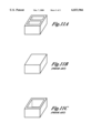
FIG. 11A shows a perspective view of a bottom storage node in accordance with the present invention; and
FIGS. 11B and 11C show perspective views of a prior art stack storage node and a prior art crown storage node, respectively.
DETAILED DESCRIPTION OF THE PREFERRED EMBODIMENT
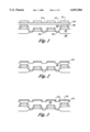
Referring to FIG. 1, a single crystal P-type substrate 100 is used for the preferred embodiment. A thick field oxide region (FOX) 102, is created using conventional methods for the purposes of isolation. Generally speaking, the FOX 102 region is created via photolithography and dry etching steps to etch a silicon nitride/silicon dioxide composite layer. After the photoresist is removed and wet cleaned, a thermo-oxidation in an oxygen-steam ambient is used to form the FOX 102 region, to a thickness of about 3,000 to 8,000 angstroms. Source and drain regions 104 are formed in the substrate 100 and gates 106 are created atop the substrate. These steps are well-known in the art and will not be discussed further herein.
Still referring to FIG. 1, an insulative silicon oxide layer 108 is deposited by using LPCVD. Next, a polysilicon layer 110 is deposited over the silicon oxide layer 108. In the preferred embodiment, the polysilicon layer 110 is deposited by conventional chemical vapor deposition (CVD). The polysilicon layer 110 has a thickness of about 500 to 2000 angstroms in the preferred embodiment. A photoresist mask layer 112 is deposited over the polysilicon layer 110. The photoresist mask layer is patterned and developed to expose a bit line contact 114 and a storage node contact 115. An anisotropic etching step is used to etch the polysilicon layer 110 and the oxide layer 108 and is controlled to stop about 300 to 1000 angstroms into the silicon oxide layer 108. After stripping of the photoresist 112, the resulting structure is shown in FIG. 2.
Referring to FIG. 3, another polysilicon layer is deposited by conventional CVD and is anisotropically etched to form polysilicon spacers 116 along the side walls of the polysilicon layer 110 and the oxide layer 108.
Referring to FIG. 4, using the polysilicon spacers 116 and the polysilicon layer 110 as a mask, the oxide layer 108 is etched until the substrate 100 is reached to form a bit line contact opening 118 and a storage node contact opening 119.
Referring to FIG. 5, the polysilicon layer 110 and polysilicon spacers 116 are removed by any conventional dry or wet etching process.
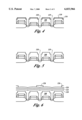
Referring to FIG. 6, a polysilicon layer 120 is deposited over the oxide layer 108 and into the bit line contact opening 118 and the storage node contact opening 119. In the preferred embodiment, the polysilicon layer 120 is deposited by CVD. The polysilicon layer 120 has a thickness of about 1000 to 2000 angstroms in the preferred embodiment. A tungsten silicide layer 122 is then deposited onto the polysilicon layer 120 by CVD and is preferably about 1000 to 2000 angstroms thick. Then, a silicon nitride or silicon oxide layer 124 is deposited onto the tungsten silicide layer 122 by LPCVD and is preferably about 1000 to 3000 angstroms thick. A photoresist mask layer 126 is deposited over the silicon nitride or silicon oxide layer 124. The photoresist mask layer 126 is patterned and developed, resulting in the structure shown in FIG. 6.
Referring to FIG. 7, the silicon nitride or silicon oxide layer 124, the tungsten silicide layer 122, and the polysilicon layer 120 are etched until the silicon oxide layer 108 is reached. This etching creates a polysilicon plug 128 in the storage node contact opening 119 and an intermediate structure 130 above the bit line contact opening 118.
Referring to FIG. 8, using conventional photolithography and anisotropic etching techniques (such as reactive ion etching), silicon nitride or silicon oxide spacers 132 are formed on the sidewalls of the intermediate structure 130. Next, a polysilicon layer 134 is deposited by using CVD. The polysilicon layer 134 is preferably about 6000 to 10000 angstroms thick. A photoresist mask layer 136 is deposited over the polysilicon layer 134. The photoresist mask layer 136 is patterned and developed, resulting in the structure shown in FIG. 8.
Referring to FIG. 9, using the photoresist layer 136 as a mask, the polysilicon layer 134 is etched and is controlled to stop preferably 500 to 3000 angstroms into the polysilicon layer 134. Then, the photoresist layer 136 is removed. Silicon dioxide is deposited and silicon oxide spacers 138 are formed on the sidewalls of the polysilicon layer 134 by reactive ion etching.
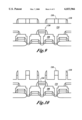
Turning to FIG. 10, the polysilicon layer 134 is etched using the oxide spacers 138 as a hard mask. The etching is stopped at the silicon oxide or silicon nitride layer 124. The oxide spacers 138 are then removed. In this manner, the 8-shaped bottom storage node of the capacitor is formed.
As is readily seen in FIG. 11A, an 8-shaped bottom storage node according to the present invention has increased surface area by which to store charge. The 8-shaped storage node shown in FIG. 11A has more surface area than previously used stack and crown storage nodes shown in FIGS. 11B and 11C, respectively. In addition, the 8-shaped storage node is stronger than the crown-shaped storage node as a result of its structure.
Finally, a thin dielectric layer is typically deposited over the bottom storage node and a plate polysilicon layer is deposited to form the upper storage node of the capacitor. These conventional "finishing" steps are known in the art and will not be discussed further herein.
While the preferred embodiment of the invention has been illustrated and described, it will be appreciated that various changes can be made therein without departing from the spirit and scope of the invention.

Claims (5)

The embodiments of the invention in which an exclusive property or privilege is claimed are defined as follows:
1. A method for manufacturing a bottom storage node of a capacitor on a substrate, the method comprising the steps of:
forming a first dielectric layer onto said substrate;
forming a first conducting layer onto said first dielectric layer;
patterning and etching said first dielectric layer and said first conducting layer, stopping within said first dielectric layer, to form a bit line contact and a storage node contact;
forming first sidewall spacers on the sides of said first dielectric layer and said first conducting layer;
using said first sidewall spacers and said first conducting layer as a mask, etching through said first dielectric layer to form a bit line contact opening and a storage node contact opening;
removing said first sidewall spacers and said first conducting layer;
forming a second conducting layer onto said first dielectric layer and into said bit line contact opening and said storage node contact opening;
forming a third conducting layer onto said second conducting layer;
forming a second dielectric layer onto said third conducting layer;
patterning and etching said second conducting layer, said third conducting layer, and said second dielectric layer to form a plug in said storage node contact opening and to form an intermediate structure above said bit line contact opening;
forming second sidewall spacers on the sides of said intermediate structure;
forming a fourth conducting layer onto said second dielectric layer, said second sidewall spacers, said plug and said first dielectric layer;
patterning and etching portions of said fourth conducting layer directly above said bit line contact opening and said storage node opening, stopping within said fourth conducting layer, said patterning and etching resulting in said fourth conducting layer being formed into an 8-shape;
forming third sidewall spacers on the sides of said fourth conducting layer;
using said third sidewall spacers as a mask, etching said fourth conducting layer, stopping at said intermediate structure; and
removing said third sidewall spacers.
2. The method of claim 1, wherein said first dielectric layer is formed of silicon oxide.
3. The method of claim 1, wherein said first conducting layer, said second conducting layer, and said fourth conducting layer are formed of polysilicon.
4. The method of claim 1, wherein said second dielectric layer is selected from a group consisting of silicon nitride or silicon oxide.
5. The method of claim 1, wherein said third conducting layer is formed of tungsten silicide.
US09/189,066 1998-11-09 1998-11-09 Method for making an 8-shaped storage node DRAM cell Expired - Fee Related US6033966A (en)

Priority Applications (2)

Application Number Priority Date Filing Date Title
US09/189,066 US6033966A (en) 1998-11-09 1998-11-09 Method for making an 8-shaped storage node DRAM cell
TW088106107A TW456000B (en) 1998-11-09 1999-04-16 Method for making an 8-shaped storage node DRAM cell

Applications Claiming Priority (1)

Application Number Priority Date Filing Date Title
US09/189,066 US6033966A (en) 1998-11-09 1998-11-09 Method for making an 8-shaped storage node DRAM cell

Publications (1)

Publication Number Publication Date
US6033966A true US6033966A (en) 2000-03-07

Family

ID=22695776

Family Applications (1)

Application Number Title Priority Date Filing Date
US09/189,066 Expired - Fee Related US6033966A (en) 1998-11-09 1998-11-09 Method for making an 8-shaped storage node DRAM cell

Country Status (2)

Country Link
US (1) US6033966A (en)
TW (1) TW456000B (en)

Cited By (4)

* Cited by examiner, † Cited by third party
Publication number Priority date Publication date Assignee Title
US6103588A (en) * 1998-07-24 2000-08-15 Vanguard International Semiconductor Corporation Method of forming a contact hole in a semiconductor device
US6268246B1 (en) * 1998-09-21 2001-07-31 Texas Instruments Incorporated Method for fabricating a memory cell
US6335237B1 (en) * 2000-03-03 2002-01-01 Micron Technology, Inc. Methods of forming capacitor and bitline structures
US20080113483A1 (en) * 2006-11-15 2008-05-15 Micron Technology, Inc. Methods of etching a pattern layer to form staggered heights therein and intermediate semiconductor device structures

Citations (4)

* Cited by examiner, † Cited by third party
Publication number Priority date Publication date Assignee Title
US5444005A (en) * 1993-05-19 1995-08-22 Samsung Electronics Co., Ltd. Method for manufacturing a capacitor of a semiconductor memory device
US5604146A (en) * 1996-06-10 1997-02-18 Vanguard International Semiconductor Corporation Method to fabricate a semiconductor memory device having an E-shaped storage node
US5710073A (en) * 1996-01-16 1998-01-20 Vanguard International Semiconductor Corporation Method for forming interconnections and conductors for high density integrated circuits
US5712202A (en) * 1995-12-27 1998-01-27 Vanguard International Semiconductor Corporation Method for fabricating a multiple walled crown capacitor of a semiconductor device

Patent Citations (4)

* Cited by examiner, † Cited by third party
Publication number Priority date Publication date Assignee Title
US5444005A (en) * 1993-05-19 1995-08-22 Samsung Electronics Co., Ltd. Method for manufacturing a capacitor of a semiconductor memory device
US5712202A (en) * 1995-12-27 1998-01-27 Vanguard International Semiconductor Corporation Method for fabricating a multiple walled crown capacitor of a semiconductor device
US5710073A (en) * 1996-01-16 1998-01-20 Vanguard International Semiconductor Corporation Method for forming interconnections and conductors for high density integrated circuits
US5604146A (en) * 1996-06-10 1997-02-18 Vanguard International Semiconductor Corporation Method to fabricate a semiconductor memory device having an E-shaped storage node

Cited By (6)

* Cited by examiner, † Cited by third party
Publication number Priority date Publication date Assignee Title
US6103588A (en) * 1998-07-24 2000-08-15 Vanguard International Semiconductor Corporation Method of forming a contact hole in a semiconductor device
US6268246B1 (en) * 1998-09-21 2001-07-31 Texas Instruments Incorporated Method for fabricating a memory cell
US6335237B1 (en) * 2000-03-03 2002-01-01 Micron Technology, Inc. Methods of forming capacitor and bitline structures
US6433994B2 (en) 2000-03-03 2002-08-13 Micron Technology, Inc. Capacitor constructions
US6636415B2 (en) 2000-03-03 2003-10-21 Micron Technology, Inc. Capacitor constructions, methods of forming bitlines, and methods of forming capacitor and bitline structures
US20080113483A1 (en) * 2006-11-15 2008-05-15 Micron Technology, Inc. Methods of etching a pattern layer to form staggered heights therein and intermediate semiconductor device structures

Also Published As

Publication number Publication date
TW456000B (en) 2001-09-21

Similar Documents

Publication Publication Date Title
US6037216A (en) Method for simultaneously fabricating capacitor structures, for giga-bit DRAM cells, and peripheral interconnect structures, using a dual damascene process
US6022776A (en) Method of using silicon oxynitride to improve fabricating of DRAM contacts and landing pads
US6359299B1 (en) Apparatus and method for forming controlled deep trench top isolation layers
US7595236B2 (en) Method for production of semiconductor device having a hole extending through a first insulating film, a second insulating film and a third insulating film
US20050253179A1 (en) Capacitor and method of manufacturing the same
US6100137A (en) Etch stop layer used for the fabrication of an overlying crown shaped storage node structure
JPH10321814A (en) Planarization technique for dram cell capacitor electrode
US6214688B1 (en) Methods of forming integrated circuit capacitors having U-shaped electrodes
US20060199332A1 (en) Method of forming storage node of capacitor in semiconductor memory, and structure therefor
US6569729B1 (en) Method of fabricating three dimensional CMOSFET devices for an embedded DRAM application
US5998259A (en) Method of fabricating dual cylindrical capacitor
US5457063A (en) Method for fabricating a capacitor for a dynamic random access memory cell
JP3233051B2 (en) Method for manufacturing semiconductor device
GB2336942A (en) Method for fabricating a DRAM cell capacitor
US5231044A (en) Method of making semiconductor memory elements
US5770510A (en) Method for manufacturing a capacitor using non-conformal dielectric
US5550077A (en) DRAM cell with a comb-type capacitor
US5913129A (en) Method of fabricating a capacitor structure for a dynamic random access memory
US6548348B1 (en) Method of forming a storage node contact hole in a porous insulator layer
US6143605A (en) Method for making a DRAM capacitor using a double layer of insitu doped polysilicon and undoped amorphous polysilicon with HSG polysilicon
JP2770789B2 (en) Method for manufacturing semiconductor memory device
US6674111B2 (en) Semiconductor device having a logic transistor therein
US6136716A (en) Method for manufacturing a self-aligned stacked storage node DRAM cell
US5952039A (en) Method for manufacturing DRAM capacitor
US5681774A (en) Method of fabricating a toothed-shape capacitor node using a thin oxide as a mask

Legal Events

Date Code Title Description
AS Assignment

Owner name: WORLDWIDE SEMICONDUCTOR MANUFACTURING CORPORATION,

Free format text: ASSIGNMENT OF ASSIGNORS INTEREST;ASSIGNOR:LINLIU, KUNG;REEL/FRAME:009634/0655

Effective date: 19981016

AS Assignment

Owner name: TAIWAN SEMICONDUCTOR MANUFACTURING CO., LTD., TAIW

Free format text: ASSIGNMENT OF ASSIGNORS INTEREST;ASSIGNOR:WORLDWIDE SEMICONDUCTOR MANUFACTURING CORP.;REEL/FRAME:010958/0881

Effective date: 20000601

REMI Maintenance fee reminder mailed
LAPS Lapse for failure to pay maintenance fees
FP Lapsed due to failure to pay maintenance fee

Effective date: 20040307

STCH Information on status: patent discontinuation

Free format text: PATENT EXPIRED DUE TO NONPAYMENT OF MAINTENANCE FEES UNDER 37 CFR 1.362