US6033981A - Keyhole-free process for high aspect ratio gap filing - Google Patents
Keyhole-free process for high aspect ratio gap filing Download PDFInfo
- Publication number
- US6033981A US6033981A US09/358,988 US35898899A US6033981A US 6033981 A US6033981 A US 6033981A US 35898899 A US35898899 A US 35898899A US 6033981 A US6033981 A US 6033981A
- Authority
- US
- United States
- Prior art keywords
- conducting lines
- oxide layer
- hdp oxide
- conducting
- overlying
- Prior art date
- Legal status (The legal status is an assumption and is not a legal conclusion. Google has not performed a legal analysis and makes no representation as to the accuracy of the status listed.)
- Expired - Lifetime
Links
Images


Classifications
-
- H—ELECTRICITY
- H01—ELECTRIC ELEMENTS
- H01L—SEMICONDUCTOR DEVICES NOT COVERED BY CLASS H10
- H01L21/00—Processes or apparatus adapted for the manufacture or treatment of semiconductor or solid state devices or of parts thereof
- H01L21/70—Manufacture or treatment of devices consisting of a plurality of solid state components formed in or on a common substrate or of parts thereof; Manufacture of integrated circuit devices or of parts thereof
- H01L21/71—Manufacture of specific parts of devices defined in group H01L21/70
- H01L21/768—Applying interconnections to be used for carrying current between separate components within a device comprising conductors and dielectrics
- H01L21/76801—Applying interconnections to be used for carrying current between separate components within a device comprising conductors and dielectrics characterised by the formation and the after-treatment of the dielectrics, e.g. smoothing
- H01L21/76829—Applying interconnections to be used for carrying current between separate components within a device comprising conductors and dielectrics characterised by the formation and the after-treatment of the dielectrics, e.g. smoothing characterised by the formation of thin functional dielectric layers, e.g. dielectric etch-stop, barrier, capping or liner layers
- H01L21/76834—Applying interconnections to be used for carrying current between separate components within a device comprising conductors and dielectrics characterised by the formation and the after-treatment of the dielectrics, e.g. smoothing characterised by the formation of thin functional dielectric layers, e.g. dielectric etch-stop, barrier, capping or liner layers formation of thin insulating films on the sidewalls or on top of conductors
-
- H—ELECTRICITY
- H01—ELECTRIC ELEMENTS
- H01L—SEMICONDUCTOR DEVICES NOT COVERED BY CLASS H10
- H01L21/00—Processes or apparatus adapted for the manufacture or treatment of semiconductor or solid state devices or of parts thereof
- H01L21/70—Manufacture or treatment of devices consisting of a plurality of solid state components formed in or on a common substrate or of parts thereof; Manufacture of integrated circuit devices or of parts thereof
- H01L21/71—Manufacture of specific parts of devices defined in group H01L21/70
- H01L21/768—Applying interconnections to be used for carrying current between separate components within a device comprising conductors and dielectrics
- H01L21/76801—Applying interconnections to be used for carrying current between separate components within a device comprising conductors and dielectrics characterised by the formation and the after-treatment of the dielectrics, e.g. smoothing
- H01L21/76837—Filling up the space between adjacent conductive structures; Gap-filling properties of dielectrics
-
- H—ELECTRICITY
- H01—ELECTRIC ELEMENTS
- H01L—SEMICONDUCTOR DEVICES NOT COVERED BY CLASS H10
- H01L21/00—Processes or apparatus adapted for the manufacture or treatment of semiconductor or solid state devices or of parts thereof
- H01L21/70—Manufacture or treatment of devices consisting of a plurality of solid state components formed in or on a common substrate or of parts thereof; Manufacture of integrated circuit devices or of parts thereof
- H01L21/71—Manufacture of specific parts of devices defined in group H01L21/70
- H01L21/768—Applying interconnections to be used for carrying current between separate components within a device comprising conductors and dielectrics
- H01L21/76897—Formation of self-aligned vias or contact plugs, i.e. involving a lithographically uncritical step
-
- H—ELECTRICITY
- H01—ELECTRIC ELEMENTS
- H01L—SEMICONDUCTOR DEVICES NOT COVERED BY CLASS H10
- H01L21/00—Processes or apparatus adapted for the manufacture or treatment of semiconductor or solid state devices or of parts thereof
- H01L21/02—Manufacture or treatment of semiconductor devices or of parts thereof
- H01L21/02104—Forming layers
- H01L21/02107—Forming insulating materials on a substrate
- H01L21/02109—Forming insulating materials on a substrate characterised by the type of layer, e.g. type of material, porous/non-porous, pre-cursors, mixtures or laminates
- H01L21/02112—Forming insulating materials on a substrate characterised by the type of layer, e.g. type of material, porous/non-porous, pre-cursors, mixtures or laminates characterised by the material of the layer
- H01L21/02123—Forming insulating materials on a substrate characterised by the type of layer, e.g. type of material, porous/non-porous, pre-cursors, mixtures or laminates characterised by the material of the layer the material containing silicon
- H01L21/0217—Forming insulating materials on a substrate characterised by the type of layer, e.g. type of material, porous/non-porous, pre-cursors, mixtures or laminates characterised by the material of the layer the material containing silicon the material being a silicon nitride not containing oxygen, e.g. SixNy or SixByNz
-
- H—ELECTRICITY
- H01—ELECTRIC ELEMENTS
- H01L—SEMICONDUCTOR DEVICES NOT COVERED BY CLASS H10
- H01L21/00—Processes or apparatus adapted for the manufacture or treatment of semiconductor or solid state devices or of parts thereof
- H01L21/02—Manufacture or treatment of semiconductor devices or of parts thereof
- H01L21/02104—Forming layers
- H01L21/02107—Forming insulating materials on a substrate
- H01L21/02109—Forming insulating materials on a substrate characterised by the type of layer, e.g. type of material, porous/non-porous, pre-cursors, mixtures or laminates
- H01L21/02205—Forming insulating materials on a substrate characterised by the type of layer, e.g. type of material, porous/non-porous, pre-cursors, mixtures or laminates the layer being characterised by the precursor material for deposition
- H01L21/02208—Forming insulating materials on a substrate characterised by the type of layer, e.g. type of material, porous/non-porous, pre-cursors, mixtures or laminates the layer being characterised by the precursor material for deposition the precursor containing a compound comprising Si
- H01L21/02211—Forming insulating materials on a substrate characterised by the type of layer, e.g. type of material, porous/non-porous, pre-cursors, mixtures or laminates the layer being characterised by the precursor material for deposition the precursor containing a compound comprising Si the compound being a silane, e.g. disilane, methylsilane or chlorosilane
-
- H—ELECTRICITY
- H01—ELECTRIC ELEMENTS
- H01L—SEMICONDUCTOR DEVICES NOT COVERED BY CLASS H10
- H01L21/00—Processes or apparatus adapted for the manufacture or treatment of semiconductor or solid state devices or of parts thereof
- H01L21/02—Manufacture or treatment of semiconductor devices or of parts thereof
- H01L21/02104—Forming layers
- H01L21/02107—Forming insulating materials on a substrate
- H01L21/02225—Forming insulating materials on a substrate characterised by the process for the formation of the insulating layer
- H01L21/0226—Forming insulating materials on a substrate characterised by the process for the formation of the insulating layer formation by a deposition process
- H01L21/02263—Forming insulating materials on a substrate characterised by the process for the formation of the insulating layer formation by a deposition process deposition from the gas or vapour phase
- H01L21/02271—Forming insulating materials on a substrate characterised by the process for the formation of the insulating layer formation by a deposition process deposition from the gas or vapour phase deposition by decomposition or reaction of gaseous or vapour phase compounds, i.e. chemical vapour deposition
- H01L21/02274—Forming insulating materials on a substrate characterised by the process for the formation of the insulating layer formation by a deposition process deposition from the gas or vapour phase deposition by decomposition or reaction of gaseous or vapour phase compounds, i.e. chemical vapour deposition in the presence of a plasma [PECVD]
-
- H—ELECTRICITY
- H01—ELECTRIC ELEMENTS
- H01L—SEMICONDUCTOR DEVICES NOT COVERED BY CLASS H10
- H01L21/00—Processes or apparatus adapted for the manufacture or treatment of semiconductor or solid state devices or of parts thereof
- H01L21/02—Manufacture or treatment of semiconductor devices or of parts thereof
- H01L21/04—Manufacture or treatment of semiconductor devices or of parts thereof the devices having at least one potential-jump barrier or surface barrier, e.g. PN junction, depletion layer or carrier concentration layer
- H01L21/18—Manufacture or treatment of semiconductor devices or of parts thereof the devices having at least one potential-jump barrier or surface barrier, e.g. PN junction, depletion layer or carrier concentration layer the devices having semiconductor bodies comprising elements of Group IV of the Periodic System or AIIIBV compounds with or without impurities, e.g. doping materials
- H01L21/30—Treatment of semiconductor bodies using processes or apparatus not provided for in groups H01L21/20 - H01L21/26
- H01L21/31—Treatment of semiconductor bodies using processes or apparatus not provided for in groups H01L21/20 - H01L21/26 to form insulating layers thereon, e.g. for masking or by using photolithographic techniques; After treatment of these layers; Selection of materials for these layers
- H01L21/3105—After-treatment
- H01L21/311—Etching the insulating layers by chemical or physical means
- H01L21/31105—Etching inorganic layers
- H01L21/31111—Etching inorganic layers by chemical means
- H01L21/31116—Etching inorganic layers by chemical means by dry-etching
-
- H—ELECTRICITY
- H01—ELECTRIC ELEMENTS
- H01L—SEMICONDUCTOR DEVICES NOT COVERED BY CLASS H10
- H01L21/00—Processes or apparatus adapted for the manufacture or treatment of semiconductor or solid state devices or of parts thereof
- H01L21/02—Manufacture or treatment of semiconductor devices or of parts thereof
- H01L21/04—Manufacture or treatment of semiconductor devices or of parts thereof the devices having at least one potential-jump barrier or surface barrier, e.g. PN junction, depletion layer or carrier concentration layer
- H01L21/18—Manufacture or treatment of semiconductor devices or of parts thereof the devices having at least one potential-jump barrier or surface barrier, e.g. PN junction, depletion layer or carrier concentration layer the devices having semiconductor bodies comprising elements of Group IV of the Periodic System or AIIIBV compounds with or without impurities, e.g. doping materials
- H01L21/30—Treatment of semiconductor bodies using processes or apparatus not provided for in groups H01L21/20 - H01L21/26
- H01L21/31—Treatment of semiconductor bodies using processes or apparatus not provided for in groups H01L21/20 - H01L21/26 to form insulating layers thereon, e.g. for masking or by using photolithographic techniques; After treatment of these layers; Selection of materials for these layers
- H01L21/314—Inorganic layers
- H01L21/316—Inorganic layers composed of oxides or glassy oxides or oxide based glass
- H01L21/31604—Deposition from a gas or vapour
- H01L21/31608—Deposition of SiO2
- H01L21/31612—Deposition of SiO2 on a silicon body
Definitions
- the present invention relates to the fabrication of semiconductor devices, and more particularly, to a method to eliminate shorts between adjacent conducting lines due to interlevel dielectric voids, known as keyholes, in the manufacture of integrated circuits.
- Inter-electrode spacings of 0.2 microns are now in fabrication. As these spacings are reduced, and the conductor height to spacing ratio approaches 4:1, it is difficult to deposit dielectric material over these electrodes without creating gaps or voids in the dielectric material.
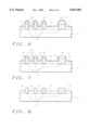
- FIG. 1 a cross-section of two conducting lines 44 patterned on substrate 40 in an integrated circuit is shown.
- a layer of dielectric 46 comprised of silicon oxide overlays the conducting lines and the surface of the substrate 40.
- the conducting lines 44 have a spacing S1 of about 0.2 microns or less.
- the aspect ratio of height to width of the gap between the conducting lines is currently about 2:1, but is becoming higher.
- air gaps, voids, or keyholes 42 will form in the dielectric oxide layer 46 in the area between the conducting lines 44.
- Air gaps in the dielectric can be helpful because the dielectric constant of air is much less than that of silicon oxide.
- the capacitive coupling between the two transistors can be reduced by the air gap. This improves circuit performance.
- These voids can cause real problems, however, in situations where the compromised integrity of the dielectric can allow a shorting condition to occur.
- DRAM dynamic random access memory
- FIG. 2 demonstrates the same problem where silicon nitride spacers 48 are deposited along the conducting line 44 sidewall.
- the aspect ratio is higher than 2:1.
- Subsequent deposition of the dielectric oxide layer 46 will again result in the formation of a keyhole 42.
- U.S. Pat. No. 5,665,657 to Lee teaches a method to remove voids in spin on glass layers by using an etch and fill method.
- U.S. Pat. No. 5,858,870 to Zheng et al teaches a method to fill gaps and planarize the dielectric layer using an anti-reflective coating with a chemical-mechanical polishing (CMP) etch stop.
- CMP chemical-mechanical polishing
- U.S. Pat. No. 5,817,567 to Jang et al teaches a method of shallow trench isolation (STI) where a layer of hard dielectric material is placed over a conformal silicon oxide. This is then planarized using CMP.
- STI shallow trench isolation
- 5,728,621 to Zheng et al teaches a method of STI planarization using a combination of high-density plasma (HDP) oxide and spin-on-glass (SOG) layers.
- HDP high-density plasma
- SOG spin-on-glass
- U.S. Pat. No. 5,721,173 to Yano et al teaches a method of STI using selective etching of dielectric films.
- U.S. Pat. No. 5,679,606 to Wang et al teaches a method where interlevel dielectric structures are formed using an in-situ multi-step electron cyclotron resonance (ECR) oxide deposition process.
- ECR electron cyclotron resonance
- a principal object of the present invention is to provide an effective and very manufacturable method of depositing dielectric oxides over closely spaced conducting lines free of voids (or keyholes) in the manufacture of integrated circuits.
- a further object of the present invention is to provide keyhole free gap filling using a two step high-density plasma (HDP) oxide.
- HDP high-density plasma
- a yet further object of the present invention is to provide a method to fill gaps without forming voids.
- a new method for depositing dielectric oxide in an integrated circuit prevents conductive shorts caused by air voids in the dielectric layer between narrowly spaced adjacent conductive lines.
- a semiconductor substrate is provided having narrowly spaced first conductive lines.
- the conductive lines may be MOS transistor gates, metal traces, or polysilicon traces.
- An HDP oxide layer is formed overlying the first conductive lines and the substrate. This oxide layer is etched back slightly exposing a portion of the sidewalls of the conductive lines. The entire surface is then covered using a nitride deposition. The peaks of the nitride, which correspond to the location of the conductive lines, are removed exposing the oxide layer.
- the exposed oxide and nitride are etched away over the conducting lines leaving a portion of the inter-electrode spacing filled with oxide. Silicon nitride spacers are then deposited along the electrode sidewalls. A second deposition of oxide is then performed with no voids formed since the depth of the interelectrode spacing is now reduced.
- FIGS. 1 and 2 schematically illustrate in cross-section partially completed prior art integrated circuits showing the problem of air voids inducing conductive shorts.
- FIGS. 3 through 10 schematically illustrate in cross-sectional representation a preferred embodiment of the present invention.
- FIG. 11 schematically illustrates in cross-sectional representation an alternative embodiment of the present invention.
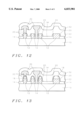
- FIG. 12 illustrates in cross-sectional representation a completed integrated circuit device fabricated according to the preferred embodiment of the present invention.
- FIG. 13 schematically illustrates in cross-sectional representation an undesirable embodiment of the invention.
- the present invention will be shown applied to the deposition of a dielectric between two closely spaced conducting lines.
- the present invention might be applied to closely spaced polysilicon traces overlying thick field oxide.
- polysilicon gate electrodes overlying gate oxide, metal traces overlying thick field oxide, or metal traces overlying source and drain structures could be substituted in the preferred embodiments.
- Such metal traces could be comprised preferably of aluminum, copper, or an alloy of aluminum and copper. Any application where metal or polysilicon traces or polysilicon gates are closely spaced can cause air voids to occur in the dielectric layer.
- the present invention will solve the potential contact shorting problem in any of these applications.
- Conductive lines 12 are patterned as is conventional in the art. Conductive lines 12 have a typical spacing of between approximately 0.10 to 0.35 microns, and a typical thickness of between approximately 2000 to 6000 angstroms. This results in a thickness to spacing ratio of the conductive lines more than 2:1.
- a high-density plasma (HDP) oxide layer 14 is then applied using a SiH 4 and O 2 source, forming mounds over the conductive lines.
- the oxide layer 14 has a thickness of between approximately 1000 to 3000 angstroms, and is approximately 50% of the conductive line 12 height.
- the oxide layer 14 is isotropically etched as is conventional in the art so that a portion of the sidewalls is exposed. Typically, this will be a wet etch dip such as a buffered oxide etch (BOE). However, if the conductors are metal, a dry isotropic etch such as CF 4 or CHF 3 will be used. Portions 18 of the first HDP oxide remain over the top surfaces of the conductors, as shown. This etch will remove any keyholes that might have formed between the conductors.
- a wet etch dip such as a buffered oxide etch (BOE).
- BOE buffered oxide etch
- CF 4 or CHF 3 dry isotropic etch
- a silicon nitride layer 16 is deposited over the entire surface to a thickness of between about 100 and 500 Angstroms.
- chemical mechanical polishing is performed removing the peaks of the nitride layer 16 and exposing oxide layer 18 over the conductive lines 12.
- the oxide layer 14 between the conductors is protected by the silicon nitride layer 16.
- a wet etch is used to completely remove the exposed oxide layer 18 overlying the conductive lines 12.
- Wet etch chemistry may include a BOE or a dilute HF.
- an isotropic etch such as CO, CF 4 or CHF 3 with a high selectivity between SiN and metal will be used. This is followed by a nitride wet dip of, for example, H 3 PO 4 , completely removing the silicon nitride layer 16. The result is shown in FIG. 8.
- a layer of silicon nitride is deposited and anisotropically etched back to leave silicon nitride spacers 20 on the sidewalls of the conductors. These spacers 20 will be used to form a self-aligned contact between narrowly spaced conducting lines.
- a second HDP oxide layer 22 is deposited to a thickness of between about 1000 and 3000 angstroms. Since the first HDP oxide layer 14 has reduced the aspect ratio of the gap, this second HDP oxide layer 22 completely fills the gap between the conducting lines without voids.
- FIG. 11 illustrates a continuation of the process from FIG. 8, where nitride spacers are not included.
- a second HDP oxide layer 22 is deposited without voids. This process flow may be desirable for wider line spacing where self-aligned contacts are not needed.
- a self-aligned contact opening is made through the HDP oxide layers 22 and 14 to one of the underlying semiconductor device structures, not shown.
- the silicon nitride spacers 20 narrow the contact opening between the conducting lines 12.
- a second conducting line 30 (on right) is shown within the contact opening. Also shown is a conducting line 30 (on left) contacting one of the lower conducting lines 12
- a passivation layer 32 completes the integrated circuit device.
- FIG. 13 illustrates the significance of all of the steps in the inventive process. Eliminating the nitride deposition (FIG. 6) step, the CMP polishing (FIG. 7), and the oxide and nitride dips (FIG. 8) will result in an extra portion of spacers 20 above the conducting lines 12. If the oxide 18 above the conducting lines 12 is completely covered by the nitride spacer 20, contact from a second conductor 30 cannot be made to the conducting line 12. The result is referred to as a "blind contact,” as shown below the conducting line 30 on the left.
- this novel approach to gap filling eliminates shorting of conductive material through voids in the dielectric layer between narrowly spaced adjacent conducting lines, MOS gates, or gaps. Further, the process of the present invention provides a very manufacturable process.
Landscapes
- Engineering & Computer Science (AREA)
- Physics & Mathematics (AREA)
- Condensed Matter Physics & Semiconductors (AREA)
- General Physics & Mathematics (AREA)
- Manufacturing & Machinery (AREA)
- Computer Hardware Design (AREA)
- Microelectronics & Electronic Packaging (AREA)
- Power Engineering (AREA)
- Internal Circuitry In Semiconductor Integrated Circuit Devices (AREA)
Abstract
A method to eliminate voids in the dielectric oxide between closely spaced conducting lines is achieved. A substrate is provided. Narrowly spaced conductive lines are provided on the substrate. A high density plasma (HDP) dielectric layer is deposited overlying the conductive lines and the substrate. The HDP layer is etched through to expose the edges of the conducting lines. An insulating layer is deposited overlying the HDP layer and conducting lines. A chemical mechanical polishing (CMP) is used to remove the peaks of the insulating layer, exposing the HDP layer in the area overlying the conducting lines. The exposed HDP layer is etched away exposing the top surface of the conducting lines. The insulating layer is then selectively etched away. Spacers may then be added along the sidewalls of the conductor. Finally, a second HDP layer is deposited overlying the first dielectric layer and conducting lines free from voids. The integrated circuit device is completed.
Description
(1) Field of the Invention
The present invention relates to the fabrication of semiconductor devices, and more particularly, to a method to eliminate shorts between adjacent conducting lines due to interlevel dielectric voids, known as keyholes, in the manufacture of integrated circuits.
(2) Description of the Prior Art
Feature size reduction is essential for realizing increased device content and higher switching speeds on integrated circuits. Inter-electrode spacings of 0.2 microns are now in fabrication. As these spacings are reduced, and the conductor height to spacing ratio approaches 4:1, it is difficult to deposit dielectric material over these electrodes without creating gaps or voids in the dielectric material.
In FIG. 1, a cross-section of two conducting lines 44 patterned on substrate 40 in an integrated circuit is shown. A layer of dielectric 46 comprised of silicon oxide overlays the conducting lines and the surface of the substrate 40.
A problem typical to the art is shown in FIG. 1. The conducting lines 44 have a spacing S1 of about 0.2 microns or less. The aspect ratio of height to width of the gap between the conducting lines is currently about 2:1, but is becoming higher. At this close spacing, air gaps, voids, or keyholes 42 will form in the dielectric oxide layer 46 in the area between the conducting lines 44. These air gaps can be either helpful or harmful to the integrated circuit depending on subsequent processing. Air gaps in the dielectric can be helpful because the dielectric constant of air is much less than that of silicon oxide. The capacitive coupling between the two transistors can be reduced by the air gap. This improves circuit performance. These voids can cause real problems, however, in situations where the compromised integrity of the dielectric can allow a shorting condition to occur. For example, when contacts are made through openings in the dielectric, the presence of a keyhole could cause two contacts to be connected through the keyhole causing a short. In a dynamic random access memory (DRAM) integrated circuit, for example, two cells could be connected through a keyhole, causing a twin-bit failure.
FIG. 2 demonstrates the same problem where silicon nitride spacers 48 are deposited along the conducting line 44 sidewall. Here, because of the presence of the spacers 48, the aspect ratio is higher than 2:1. Subsequent deposition of the dielectric oxide layer 46 will again result in the formation of a keyhole 42.
Several prior art approaches attempt to address the problems of voids in the dielectric layer. U.S. Pat. No. 5,665,657 to Lee teaches a method to remove voids in spin on glass layers by using an etch and fill method. U.S. Pat. No. 5,858,870 to Zheng et al teaches a method to fill gaps and planarize the dielectric layer using an anti-reflective coating with a chemical-mechanical polishing (CMP) etch stop. U.S. Pat. No. 5,817,567 to Jang et al teaches a method of shallow trench isolation (STI) where a layer of hard dielectric material is placed over a conformal silicon oxide. This is then planarized using CMP. U.S. Pat. No. 5,728,621 to Zheng et al teaches a method of STI planarization using a combination of high-density plasma (HDP) oxide and spin-on-glass (SOG) layers. U.S. Pat. No. 5,721,173 to Yano et al teaches a method of STI using selective etching of dielectric films. U.S. Pat. No. 5,679,606 to Wang et al teaches a method where interlevel dielectric structures are formed using an in-situ multi-step electron cyclotron resonance (ECR) oxide deposition process.
A principal object of the present invention is to provide an effective and very manufacturable method of depositing dielectric oxides over closely spaced conducting lines free of voids (or keyholes) in the manufacture of integrated circuits.
A further object of the present invention is to provide keyhole free gap filling using a two step high-density plasma (HDP) oxide.
A yet further object of the present invention is to provide a method to fill gaps without forming voids.
In accordance with the object of this invention, a new method for depositing dielectric oxide in an integrated circuit is achieved. This method prevents conductive shorts caused by air voids in the dielectric layer between narrowly spaced adjacent conductive lines. A semiconductor substrate is provided having narrowly spaced first conductive lines. The conductive lines may be MOS transistor gates, metal traces, or polysilicon traces. An HDP oxide layer is formed overlying the first conductive lines and the substrate. This oxide layer is etched back slightly exposing a portion of the sidewalls of the conductive lines. The entire surface is then covered using a nitride deposition. The peaks of the nitride, which correspond to the location of the conductive lines, are removed exposing the oxide layer. The exposed oxide and nitride are etched away over the conducting lines leaving a portion of the inter-electrode spacing filled with oxide. Silicon nitride spacers are then deposited along the electrode sidewalls. A second deposition of oxide is then performed with no voids formed since the depth of the interelectrode spacing is now reduced.
In the accompanying drawings forming a material part of this description, there is shown:
FIGS. 1 and 2 schematically illustrate in cross-section partially completed prior art integrated circuits showing the problem of air voids inducing conductive shorts.
FIGS. 3 through 10 schematically illustrate in cross-sectional representation a preferred embodiment of the present invention.
FIG. 11 schematically illustrates in cross-sectional representation an alternative embodiment of the present invention.
FIG. 12 illustrates in cross-sectional representation a completed integrated circuit device fabricated according to the preferred embodiment of the present invention.
FIG. 13 schematically illustrates in cross-sectional representation an undesirable embodiment of the invention.
In the preferred embodiment, the present invention will be shown applied to the deposition of a dielectric between two closely spaced conducting lines. For example, the present invention might be applied to closely spaced polysilicon traces overlying thick field oxide. Alternately, polysilicon gate electrodes overlying gate oxide, metal traces overlying thick field oxide, or metal traces overlying source and drain structures could be substituted in the preferred embodiments. Such metal traces could be comprised preferably of aluminum, copper, or an alloy of aluminum and copper. Any application where metal or polysilicon traces or polysilicon gates are closely spaced can cause air voids to occur in the dielectric layer. The present invention will solve the potential contact shorting problem in any of these applications.
Referring now more particularly to FIG. 3, there is illustrated a portion of a partially completed integrated circuit. A substrate 10 is provided. Conductive lines 12, are patterned as is conventional in the art. Conductive lines 12 have a typical spacing of between approximately 0.10 to 0.35 microns, and a typical thickness of between approximately 2000 to 6000 angstroms. This results in a thickness to spacing ratio of the conductive lines more than 2:1.
Referring now to FIG. 4, a high-density plasma (HDP) oxide layer 14 is then applied using a SiH4 and O2 source, forming mounds over the conductive lines. The oxide layer 14 has a thickness of between approximately 1000 to 3000 angstroms, and is approximately 50% of the conductive line 12 height.
Referring now to FIG. 5, the oxide layer 14 is isotropically etched as is conventional in the art so that a portion of the sidewalls is exposed. Typically, this will be a wet etch dip such as a buffered oxide etch (BOE). However, if the conductors are metal, a dry isotropic etch such as CF4 or CHF3 will be used. Portions 18 of the first HDP oxide remain over the top surfaces of the conductors, as shown. This etch will remove any keyholes that might have formed between the conductors.
Referring now to FIG. 6, a silicon nitride layer 16, is deposited over the entire surface to a thickness of between about 100 and 500 Angstroms.
Referring now to FIG. 7, chemical mechanical polishing is performed removing the peaks of the nitride layer 16 and exposing oxide layer 18 over the conductive lines 12. The oxide layer 14 between the conductors is protected by the silicon nitride layer 16.
For non-metallic conductive lines 12, a wet etch is used to completely remove the exposed oxide layer 18 overlying the conductive lines 12. Wet etch chemistry may include a BOE or a dilute HF. For metal conductive lines 12, an isotropic etch such as CO, CF4 or CHF3 with a high selectivity between SiN and metal will be used. This is followed by a nitride wet dip of, for example, H3 PO4, completely removing the silicon nitride layer 16. The result is shown in FIG. 8.
Referring now to FIG. 9, in a preferred alternative, a layer of silicon nitride is deposited and anisotropically etched back to leave silicon nitride spacers 20 on the sidewalls of the conductors. These spacers 20 will be used to form a self-aligned contact between narrowly spaced conducting lines.
Referring now to FIG. 10, a second HDP oxide layer 22, is deposited to a thickness of between about 1000 and 3000 angstroms. Since the first HDP oxide layer 14 has reduced the aspect ratio of the gap, this second HDP oxide layer 22 completely fills the gap between the conducting lines without voids.
FIG. 11 illustrates a continuation of the process from FIG. 8, where nitride spacers are not included. A second HDP oxide layer 22 is deposited without voids. This process flow may be desirable for wider line spacing where self-aligned contacts are not needed.
Referring now to FIG. 12, a self-aligned contact opening is made through the HDP oxide layers 22 and 14 to one of the underlying semiconductor device structures, not shown. The silicon nitride spacers 20 narrow the contact opening between the conducting lines 12. A second conducting line 30 (on right) is shown within the contact opening. Also shown is a conducting line 30 (on left) contacting one of the lower conducting lines 12 A passivation layer 32 completes the integrated circuit device.
FIG. 13 illustrates the significance of all of the steps in the inventive process. Eliminating the nitride deposition (FIG. 6) step, the CMP polishing (FIG. 7), and the oxide and nitride dips (FIG. 8) will result in an extra portion of spacers 20 above the conducting lines 12. If the oxide 18 above the conducting lines 12 is completely covered by the nitride spacer 20, contact from a second conductor 30 cannot be made to the conducting line 12. The result is referred to as a "blind contact," as shown below the conducting line 30 on the left.
As has been shown in the preferred embodiment, this novel approach to gap filling eliminates shorting of conductive material through voids in the dielectric layer between narrowly spaced adjacent conducting lines, MOS gates, or gaps. Further, the process of the present invention provides a very manufacturable process.
While the invention has been particularly shown and described with reference to the preferred embodiments thereof, it will be understood by those skilled in the art that various changes in form and details may be made without departing from the spirit and scope of the invention.
Claims (25)
1. A method to eliminate the formation of voids in a gap between closely spaced conducting lines in an integrated circuit device comprising:
providing a substrate;
providing said closely spaced conducting lines having said gap therebetween on said substrate;
depositing a first HDP oxide layer overlying tops and sidewalls of said conducting lines and said substrate;
isotropically etching said first HDP oxide layer exposing an upper portion of said sidewalls of said conducting lines;
depositing an insulating layer overlying said first HDP oxide layer and said exposed conducting line sidewalls;
removing said insulating layer overlying said HDP oxide layer on said tops of said conducting lines using chemical mechanical polishing;
etching away exposed areas of said first HDP oxide layer overlying said tops of said conducting lines;
thereafter removing said insulating layer;
forming insulating spacers on said upper portion of said sidewalls of said conducting lines;
depositing a second HDP oxide layer overlying said first HDP oxide layer, said conducting lines and said insulating spacers thereby filling said gap between said conducting lines; and
completing said integrated circuit device.
2. The method according to claim 1 wherein said narrowly spaced conducting lines comprise one of the group containing: polysilicon, aluminum, copper, alloys of aluminum, and alloys of copper.
3. The method according to claim 1 wherein said closely spaced conducting lines are spaced less than about 0.01 microns apart and have a thickness of at most 6000 angstroms.
4. The method according to claim 1 wherein said first HDP oxide layer deposited using SiH4 and O2 as a silicon source and deposited to a thickness of between about 1000 and 3000 angstroms.
5. The method according to claim 1 wherein said insulating layer comprises silicon nitride deposited to a thickness of between about 100 and 500 angstroms.
6. The method according to claim 1 wherein said etching away of said first HDP oxide layer is by a wet etching process using a buffered oxide etch (BOE).
7. The method according to claim 1 wherein said etching away of said first HDP oxide layer is by a dry etching process using a chemistry of CF4 or CHF3 gases.
8. The method according to claim 1 wherein said step of removing said insulating layer is by a wet etching process using a buffered oxide etch (BOE).
9. The method according to claim 1 wherein said second HDP oxide layer is deposited using SiH4 and O2 as a silicon source to a thickness of between about 1000 and 3000 angstroms.
10. The method according to claim 1 wherein said insulating spacers comprise silicon nitride.
11. A method to form contacts in an integrated circuit device comprising:
providing semiconductor device structures formed in and on a semiconductor substrate;
depositing an insulating layer overlying said semiconductor device structures;
forming conducting lines overlying said insulating layer and contacting some of said semiconductor device structures through openings in said insulating layer wherein a gap remains between said conducting lines;
depositing a first HDP oxide layer overlying tops and sidewalls of said conducting lines and said substrate;
isotropically etching said first HDP oxide layer exposing an upper portion of said sidewalls of said conducting lines;
depositing an insulating layer overlying said first HDP oxide layer and said exposed conducting line sidewalls;
removing said insulating layer overlying said HDP oxide layer on said tops of said conducting lines using chemical mechanical polishing;
etching away exposed areas of said first HDP oxide layer overlying said tops of said conducting lines;
thereafter removing said insulating layer;
forming insulating spacers on said upper portion of said sidewalls of said conducting lines;
depositing a second HDP oxide layer overlying said first HDP oxide layer, said conducting lines and said insulating spacers thereby filling said gap between said conducting lines;
forming a self-aligned contact opening between two of said conducting lines whereby said insulating spacers act as an etch stop in forming said self-aligned contact; and
filling said self-aligned contact opening with a second conducting line to complete said formation of said contacts in the fabrication of said integrated circuit device.
12. The method according to claim 11 wherein said conducting lines comprise one of the group containing: polysilicon, aluminum, copper, alloys of aluminum, and alloys of copper.
13. The method according to claim 11 wherein said conducting lines have an aspect ratio of more than about 2:1.
14. The method according to claim 11 wherein said first HDP oxide layer deposited using SiH4 and O2 as a silicon source and deposited to a thickness of between about 1000 and 3000 angstroms.
15. The method according to claim 11 wherein said insulating layer comprises silicon nitride deposited to a thickness of between about 100 and 500 angstroms.
16. The method according to claim 11 wherein said etching away of said first HDP oxide layer is by a wet etching process using a buffered oxide etch (BOE).
17. The method according to claim 11 wherein said etching away of said first HDP oxide layer is by a dry etching process using a chemistry of CF4 or CHF3 gases.
18. The method according to claim 11 wherein said etching through of said insulating layer is by a wet etching process using a buffered oxide etch (BOE).
19. The method according to claim 11 wherein said second HDP oxide layer is deposited using SiH4 and O2 as a silicon source to a thickness of between about 1000 and 3000 angstroms.
20. The method according to claim 11 wherein said insulating spacers comprise silicon nitride.
21. The method according to claim 11 wherein said semiconductor device structures include gate electrodes and associated source and drain regions of MOS devices.
22. A method to form contacts in an integrated circuit device comprising:
providing semiconductor device structures formed in and on a semiconductor substrate wherein said semiconductor device structures include gate electrodes and associated source and drain regions of MOS devices;
depositing an insulating layer overlying said semiconductor device structures;
forming conducting lines overlying said insulating layer and contacting some of said semiconductor device structures through openings in said insulating layer wherein a gap formed between two of said conducting lines has an aspect ratio of at least 2:1;
depositing a first HDP oxide layer overlying tops and sidewalls of said conducting lines and said substrate;
isotropically etching said first HDP oxide layer exposing an upper portion of said sidewalls of said conducting lines;
depositing a silicon nitride layer overlying said first H)P oxide layer and said exposed conducting line sidewalls;
removing said insulating layer overlying said HDP oxide layer on said tops of said conducting lines using chemical mechanical polishing;
etching away exposed areas of said first HDP oxide layer overlying said tops of said conducting lines;
thereafter removing said silicon nitride layer;
forming insulating spacers on said upper portion of said sidewalls of said conducting lines;
depositing a second HDP oxide layer overlying said first HDP oxide layer, said conducting lines said insulating spacers and covering said conducting lines wherein said gap has an aspect ratio of less than 2:1 because of the presence of said first HDP oxide layer within said gap and whereby no voids are formed within said second HDP oxide layer within said gap;
forming a self-aligned contact opening between two of said conducting lines whereby said silicon nitride spacers act as an etch stop in forming said self-aligned contact; and
filling said self-aligned contact opening with a second conducting line to complete said formation of said contacts in the fabrication of said integrated circuit device.
23. The method according to claim 22 wherein said conducting lines comprise one of the group containing: polysilicon, aluminum, copper, alloys of aluminum, and alloys of copper.
24. The method according to claim 22 wherein said first HDP oxide layer is deposited to a thickness of between about 1000 and 3000 angstroms.
25. The method according to claim 22 wherein said second HDP oxide layer is deposited to a thickness of between about 1000 and 3000 angstroms.
Priority Applications (1)
| Application Number | Priority Date | Filing Date | Title |
|---|---|---|---|
| US09/358,988 US6033981A (en) | 1999-07-22 | 1999-07-22 | Keyhole-free process for high aspect ratio gap filing |
Applications Claiming Priority (1)
| Application Number | Priority Date | Filing Date | Title |
|---|---|---|---|
| US09/358,988 US6033981A (en) | 1999-07-22 | 1999-07-22 | Keyhole-free process for high aspect ratio gap filing |
Publications (1)
| Publication Number | Publication Date |
|---|---|
| US6033981A true US6033981A (en) | 2000-03-07 |
Family
ID=23411859
Family Applications (1)
| Application Number | Title | Priority Date | Filing Date |
|---|---|---|---|
| US09/358,988 Expired - Lifetime US6033981A (en) | 1999-07-22 | 1999-07-22 | Keyhole-free process for high aspect ratio gap filing |
Country Status (1)
| Country | Link |
|---|---|
| US (1) | US6033981A (en) |
Cited By (20)
| Publication number | Priority date | Publication date | Assignee | Title |
|---|---|---|---|---|
| US6133151A (en) * | 1999-05-10 | 2000-10-17 | Worldwide Semiconductor Manufacturing Corp. | HDP-CVD method for spacer formation |
| US6150238A (en) * | 1999-03-04 | 2000-11-21 | Mosel Vitelic, Inc. | Method for fabricating a trench isolation |
| US6174802B1 (en) * | 1999-06-28 | 2001-01-16 | Taiwan Semiconductor Manufacturing Company | Method for fabricating a self aligned contact which eliminates the key hole problem using a two step contact deposition |
| US6194302B1 (en) * | 1999-09-30 | 2001-02-27 | Taiwan Semiconductor Manufacturing Company | Integrated process flow to improve the electrical isolation within self aligned contact structure |
| US6358845B1 (en) | 2001-03-16 | 2002-03-19 | Taiwan Semiconductor Manufacturing Company | Method for forming inter metal dielectric |
| US6387797B1 (en) * | 1999-01-20 | 2002-05-14 | Philips Electronics No. America Corp. | Method for reducing the capacitance between interconnects by forming voids in dielectric material |
| US20020076877A1 (en) * | 2000-06-16 | 2002-06-20 | Chartered Semiconductor Manufacturing Ltd. | Method to form self-aligned, L-shaped sidewall spacers |
| US6420250B1 (en) * | 2000-03-03 | 2002-07-16 | Micron Technology, Inc. | Methods of forming portions of transistor structures, methods of forming array peripheral circuitry, and structures comprising transistor gates |
| US6433378B1 (en) * | 1999-11-02 | 2002-08-13 | Micron Technology, Inc. | Integrated circuits having material within structural gaps |
| US6541349B2 (en) | 2001-01-18 | 2003-04-01 | International Business Machines Corporation | Shallow trench isolation using non-conformal dielectric and planarizatrion |
| US20030075799A1 (en) * | 2001-10-24 | 2003-04-24 | Drynan John M. | Methods of forming conductive contacts to conductive structures, and integrated circuitry |
| US6740549B1 (en) | 2001-08-10 | 2004-05-25 | Integrated Device Technology, Inc. | Gate structures having sidewall spacers using selective deposition and method of forming the same |
| US20040188806A1 (en) * | 2003-03-31 | 2004-09-30 | Samsung Electronics Co., Ltd. | Sidewall spacer structure for self-aligned contact and method for forming the same |
| US20040266221A1 (en) * | 2003-06-30 | 2004-12-30 | Kim Sang Deok | Method of manufacturing semiconductor device |
| US20050186796A1 (en) * | 2004-02-24 | 2005-08-25 | Sis Microelectronics Corporation | Method for gap filling between metal-metal lines |
| US20060073699A1 (en) * | 2004-10-06 | 2006-04-06 | Hynix Semiconductor, Inc. | Method for fabricating semiconductor device |
| US20090181874A1 (en) * | 2008-01-11 | 2009-07-16 | Philip Frank Souter | Cleaning And/Or Treatment Compositions |
| US20110018046A1 (en) * | 2005-04-27 | 2011-01-27 | Hiroyuki Kutsukake | Method of manufacture of contact plug and interconnection layer of semiconductor device |
| US8946782B2 (en) | 2012-04-19 | 2015-02-03 | International Business Machines Corporation | Method for keyhole repair in replacement metal gate integration through the use of a printable dielectric |
| US20170053875A1 (en) * | 2013-03-13 | 2017-02-23 | Taiwan Semiconductor Manufacturing Co., Ltd. | Electro-migration barrier for cu interconnect |
Citations (11)
| Publication number | Priority date | Publication date | Assignee | Title |
|---|---|---|---|---|
| US5310700A (en) * | 1993-03-26 | 1994-05-10 | Integrated Device Technology, Inc. | Conductor capacitance reduction in integrated circuits |
| US5393709A (en) * | 1993-06-30 | 1995-02-28 | United Microelectronics Corporation | Method of making stress released VLSI structure by the formation of porous intermetal layer |
| US5494854A (en) * | 1994-08-17 | 1996-02-27 | Texas Instruments Incorporated | Enhancement in throughput and planarity during CMP using a dielectric stack containing HDP-SiO2 films |
| US5545919A (en) * | 1993-04-14 | 1996-08-13 | Matsushita Electric Industrial Co., Ltd. | Semiconductor device and method of fabricating the same |
| US5641712A (en) * | 1995-08-07 | 1997-06-24 | Motorola, Inc. | Method and structure for reducing capacitance between interconnect lines |
| US5665657A (en) * | 1995-09-18 | 1997-09-09 | Taiwan Semiconductor Manufacturing Company, Ltd | Spin-on-glass partial etchback planarization process |
| US5679606A (en) * | 1995-12-27 | 1997-10-21 | Taiwan Semiconductor Manufacturing Company, Ltd. | method of forming inter-metal-dielectric structure |
| US5721173A (en) * | 1997-02-25 | 1998-02-24 | Kabushiki Kaisha Toshiba | Method of forming a shallow trench isolation structure |
| US5728621A (en) * | 1997-04-28 | 1998-03-17 | Chartered Semiconductor Manufacturing Pte Ltd | Method for shallow trench isolation |
| US5817567A (en) * | 1997-04-07 | 1998-10-06 | Taiwan Semiconductor Manufacturing Company Ltd. | Shallow trench isolation method |
| US5858870A (en) * | 1996-12-16 | 1999-01-12 | Chartered Semiconductor Manufacturing, Ltd. | Methods for gap fill and planarization of intermetal dielectrics |
-
1999
- 1999-07-22 US US09/358,988 patent/US6033981A/en not_active Expired - Lifetime
Patent Citations (11)
| Publication number | Priority date | Publication date | Assignee | Title |
|---|---|---|---|---|
| US5310700A (en) * | 1993-03-26 | 1994-05-10 | Integrated Device Technology, Inc. | Conductor capacitance reduction in integrated circuits |
| US5545919A (en) * | 1993-04-14 | 1996-08-13 | Matsushita Electric Industrial Co., Ltd. | Semiconductor device and method of fabricating the same |
| US5393709A (en) * | 1993-06-30 | 1995-02-28 | United Microelectronics Corporation | Method of making stress released VLSI structure by the formation of porous intermetal layer |
| US5494854A (en) * | 1994-08-17 | 1996-02-27 | Texas Instruments Incorporated | Enhancement in throughput and planarity during CMP using a dielectric stack containing HDP-SiO2 films |
| US5641712A (en) * | 1995-08-07 | 1997-06-24 | Motorola, Inc. | Method and structure for reducing capacitance between interconnect lines |
| US5665657A (en) * | 1995-09-18 | 1997-09-09 | Taiwan Semiconductor Manufacturing Company, Ltd | Spin-on-glass partial etchback planarization process |
| US5679606A (en) * | 1995-12-27 | 1997-10-21 | Taiwan Semiconductor Manufacturing Company, Ltd. | method of forming inter-metal-dielectric structure |
| US5858870A (en) * | 1996-12-16 | 1999-01-12 | Chartered Semiconductor Manufacturing, Ltd. | Methods for gap fill and planarization of intermetal dielectrics |
| US5721173A (en) * | 1997-02-25 | 1998-02-24 | Kabushiki Kaisha Toshiba | Method of forming a shallow trench isolation structure |
| US5817567A (en) * | 1997-04-07 | 1998-10-06 | Taiwan Semiconductor Manufacturing Company Ltd. | Shallow trench isolation method |
| US5728621A (en) * | 1997-04-28 | 1998-03-17 | Chartered Semiconductor Manufacturing Pte Ltd | Method for shallow trench isolation |
Non-Patent Citations (4)
| Title |
|---|
| Broomfield, M., "HDP Dielectric BEOL Gapfill: A Process for Manufacturing," Advanced Semiconductor Manufacturing Conference and Workshop, 1996, ASMC 96 Proceedings, IEEE/SEMI 1996, pp. 255-258. |
| Broomfield, M., HDP Dielectric BEOL Gapfill: A Process for Manufacturing, Advanced Semiconductor Manufacturing Conference and Workshop, 1996, ASMC 96 Proceedings, IEEE/SEMI 1996, pp. 255 258. * |
| Kim, J., et al., "Characterization of the HDP-CVD Oxide as Interlayer Dielectric Material for Subs-quarter Micron CMOS," Interconnect Technology Conference, Proceedings of the IEEE 1998 International, pp. 274-276. |
| Kim, J., et al., Characterization of the HDP CVD Oxide as Interlayer Dielectric Material for Subs quarter Micron CMOS, Interconnect Technology Conference, Proceedings of the IEEE 1998 International, pp. 274 276. * |
Cited By (36)
| Publication number | Priority date | Publication date | Assignee | Title |
|---|---|---|---|---|
| US6387797B1 (en) * | 1999-01-20 | 2002-05-14 | Philips Electronics No. America Corp. | Method for reducing the capacitance between interconnects by forming voids in dielectric material |
| US6150238A (en) * | 1999-03-04 | 2000-11-21 | Mosel Vitelic, Inc. | Method for fabricating a trench isolation |
| US6133151A (en) * | 1999-05-10 | 2000-10-17 | Worldwide Semiconductor Manufacturing Corp. | HDP-CVD method for spacer formation |
| US6174802B1 (en) * | 1999-06-28 | 2001-01-16 | Taiwan Semiconductor Manufacturing Company | Method for fabricating a self aligned contact which eliminates the key hole problem using a two step contact deposition |
| US6194302B1 (en) * | 1999-09-30 | 2001-02-27 | Taiwan Semiconductor Manufacturing Company | Integrated process flow to improve the electrical isolation within self aligned contact structure |
| US6433378B1 (en) * | 1999-11-02 | 2002-08-13 | Micron Technology, Inc. | Integrated circuits having material within structural gaps |
| US6500730B1 (en) | 1999-11-02 | 2002-12-31 | Micron Technology, Inc. | Method for filling structural gaps and integrated circuitry |
| US6787877B2 (en) | 1999-11-02 | 2004-09-07 | Micron Technology, Inc. | Method for filling structural gaps and integrated circuitry |
| US6501114B2 (en) | 2000-03-03 | 2002-12-31 | Micron Technology, Inc. | Structures comprising transistor gates |
| US6420250B1 (en) * | 2000-03-03 | 2002-07-16 | Micron Technology, Inc. | Methods of forming portions of transistor structures, methods of forming array peripheral circuitry, and structures comprising transistor gates |
| US6770927B2 (en) | 2000-03-03 | 2004-08-03 | Micron Technology, Inc. | Structures comprising transistor gates |
| US20020076877A1 (en) * | 2000-06-16 | 2002-06-20 | Chartered Semiconductor Manufacturing Ltd. | Method to form self-aligned, L-shaped sidewall spacers |
| US6541349B2 (en) | 2001-01-18 | 2003-04-01 | International Business Machines Corporation | Shallow trench isolation using non-conformal dielectric and planarizatrion |
| US6358845B1 (en) | 2001-03-16 | 2002-03-19 | Taiwan Semiconductor Manufacturing Company | Method for forming inter metal dielectric |
| US6740549B1 (en) | 2001-08-10 | 2004-05-25 | Integrated Device Technology, Inc. | Gate structures having sidewall spacers using selective deposition and method of forming the same |
| US6861713B2 (en) * | 2001-10-24 | 2005-03-01 | Micron Technology, Inc. | Integrated circuitry comprising insulative collars and integrated circuitry comprising sidewall spacers over a conductive line projecting outwardly from a first insulative material |
| US7285814B2 (en) | 2001-10-24 | 2007-10-23 | Micron Technology, Inc. | Dynamic random access memory circuitry and integrated circuitry |
| US20060157767A1 (en) * | 2001-10-24 | 2006-07-20 | Drynan John M | Dynamic random assess memory circuitry and integrated circuitry |
| US20030075799A1 (en) * | 2001-10-24 | 2003-04-24 | Drynan John M. | Methods of forming conductive contacts to conductive structures, and integrated circuitry |
| US20050124163A1 (en) * | 2001-10-24 | 2005-06-09 | Drynan John M. | Dynamic random access memory circuitry comprising insulative collars |
| US7019347B2 (en) | 2001-10-24 | 2006-03-28 | Micron Technology, Inc. | Dynamic random access memory circuitry comprising insulative collars |
| US7056828B2 (en) * | 2003-03-31 | 2006-06-06 | Samsung Electronics Co., Ltd | Sidewall spacer structure for self-aligned contact and method for forming the same |
| US20040188806A1 (en) * | 2003-03-31 | 2004-09-30 | Samsung Electronics Co., Ltd. | Sidewall spacer structure for self-aligned contact and method for forming the same |
| US20040266221A1 (en) * | 2003-06-30 | 2004-12-30 | Kim Sang Deok | Method of manufacturing semiconductor device |
| US7179735B2 (en) | 2003-06-30 | 2007-02-20 | Hynix Semiconductor Inc. | Method of manufacturing semiconductor device |
| US20050186796A1 (en) * | 2004-02-24 | 2005-08-25 | Sis Microelectronics Corporation | Method for gap filling between metal-metal lines |
| US20060073699A1 (en) * | 2004-10-06 | 2006-04-06 | Hynix Semiconductor, Inc. | Method for fabricating semiconductor device |
| US20110018046A1 (en) * | 2005-04-27 | 2011-01-27 | Hiroyuki Kutsukake | Method of manufacture of contact plug and interconnection layer of semiconductor device |
| US20090181874A1 (en) * | 2008-01-11 | 2009-07-16 | Philip Frank Souter | Cleaning And/Or Treatment Compositions |
| US8946782B2 (en) | 2012-04-19 | 2015-02-03 | International Business Machines Corporation | Method for keyhole repair in replacement metal gate integration through the use of a printable dielectric |
| US9087916B2 (en) | 2012-04-19 | 2015-07-21 | International Business Machines Corporation | Method for keyhole repair in replacement metal gate integration through the use of a printable dielectric |
| US20170053875A1 (en) * | 2013-03-13 | 2017-02-23 | Taiwan Semiconductor Manufacturing Co., Ltd. | Electro-migration barrier for cu interconnect |
| US10163795B2 (en) * | 2013-03-13 | 2018-12-25 | Taiwan Semiconductor Manufacturing Co., Ltd. | Electro-migration barrier for Cu interconnect |
| US10867920B2 (en) | 2013-03-13 | 2020-12-15 | Taiwan Semiconductor Manufacturing Co., Ltd. | Electro-migration barrier for Cu interconnect |
| US11515255B2 (en) | 2013-03-13 | 2022-11-29 | Taiwan Semiconductor Manufacturing Company, Ltd. | Electro-migration barrier for interconnect |
| US11923304B2 (en) | 2013-03-13 | 2024-03-05 | Taiwan Semiconductor Manufacturing Company, Ltd. | Electro-migration barrier for interconnect |
Similar Documents
| Publication | Publication Date | Title |
|---|---|---|
| US6033981A (en) | Keyhole-free process for high aspect ratio gap filing | |
| US5702982A (en) | Method for making metal contacts and interconnections concurrently on semiconductor integrated circuits | |
| US6429477B1 (en) | Shared body and diffusion contact structure and method for fabricating same | |
| US5885883A (en) | Methods of forming trench-based isolation regions with reduced susceptibility to edge defects | |
| US5874317A (en) | Trench isolation for integrated circuits | |
| US5477074A (en) | Semiconductor structure using local planarization with self-aligned transistors | |
| US6576550B1 (en) | ‘Via first’ dual damascene process for copper metallization | |
| US5593921A (en) | Method of forming vias | |
| US20020048944A1 (en) | Multi-level circuit structure | |
| US6350682B1 (en) | Method of fabricating dual damascene structure using a hard mask | |
| US6278189B1 (en) | High density integrated circuits using tapered and self-aligned contacts | |
| US6472308B1 (en) | Borderless vias on bottom metal | |
| US6137126A (en) | Method to reduce gate-to-local interconnect capacitance using a low dielectric constant material for LDD spacer | |
| EP1390977A2 (en) | Method for fabricating vertical transistor trench capacitor dram cells | |
| KR20020045028A (en) | Method for fabricating pad without void using self-aligned contact etch process in semiconductor device | |
| US5510294A (en) | Method of forming vias for multilevel metallization | |
| US6107193A (en) | Completely removal of TiN residue on dual damascence process | |
| US6555435B2 (en) | Method to eliminate shorts between adjacent contacts due to interlevel dielectric voids | |
| US6404055B1 (en) | Semiconductor device with improved metal interconnection and method for forming the metal interconnection | |
| US6426263B1 (en) | Method for making a merged contact window in a transistor to electrically connect the gate to either the source or the drain | |
| US7084057B2 (en) | Bit line contact structure and fabrication method thereof | |
| US7211488B2 (en) | Method of forming inter-dielectric layer in semiconductor device | |
| US5847457A (en) | Structure and method of forming vias | |
| KR101021176B1 (en) | Method for forming a metal line in semiconductor device | |
| EP0929100A2 (en) | Process for controlling the height of a stud intersecting an interconnect |
Legal Events
| Date | Code | Title | Description |
|---|---|---|---|
| AS | Assignment |
Owner name: TAIWAN SEMICONDUCTOR MANUFACTURING COMPANY, TAIWAN Free format text: ASSIGNMENT OF ASSIGNORS INTEREST;ASSIGNORS:LEE, YU-HUA;WU, CHENG-MING;REEL/FRAME:010125/0081 Effective date: 19990520 |
|
| STCF | Information on status: patent grant |
Free format text: PATENTED CASE |
|
| FPAY | Fee payment |
Year of fee payment: 4 |
|
| FPAY | Fee payment |
Year of fee payment: 8 |
|
| FPAY | Fee payment |
Year of fee payment: 12 |