US6049445A - Overvoltage and electrostatic discharge protection for a receiver circuit - Google Patents

Overvoltage and electrostatic discharge protection for a receiver circuit Download PDF

Info

Publication number
US6049445A
US6049445A US09/156,111 US15611198A US6049445A US 6049445 A US6049445 A US 6049445A US 15611198 A US15611198 A US 15611198A US 6049445 A US6049445 A US 6049445A
Authority
US
United States
Prior art keywords
pass transistor
rail
potential
gate
channel mosfet
Prior art date
Legal status (The legal status is an assumption and is not a legal conclusion. Google has not performed a legal analysis and makes no representation as to the accuracy of the status listed.)
Expired - Lifetime
Application number
US09/156,111
Inventor
Robert J. Gauthier, Jr.
Steven H. Voldman
Current Assignee (The listed assignees may be inaccurate. Google has not performed a legal analysis and makes no representation or warranty as to the accuracy of the list.)
International Business Machines Corp
Original Assignee
International Business Machines Corp
Priority date (The priority date is an assumption and is not a legal conclusion. Google has not performed a legal analysis and makes no representation as to the accuracy of the date listed.)
Filing date
Publication date
Application filed by International Business Machines Corp filed Critical International Business Machines Corp
Priority to US09/156,111 priority Critical patent/US6049445A/en
Assigned to INTERNATIONAL BUSINESS MACHINES CORPORATION reassignment INTERNATIONAL BUSINESS MACHINES CORPORATION ASSIGNMENT OF ASSIGNORS INTEREST (SEE DOCUMENT FOR DETAILS). Assignors: GAUTHIER, ROBERT J., JR., VOLDMAN, STEVEN H.
Application granted granted Critical
Publication of US6049445A publication Critical patent/US6049445A/en
Anticipated expiration legal-status Critical
Expired - Lifetime legal-status Critical Current

Links

Images

Classifications

    • HELECTRICITY
    • H01ELECTRIC ELEMENTS
    • H01LSEMICONDUCTOR DEVICES NOT COVERED BY CLASS H10
    • H01L27/00Devices consisting of a plurality of semiconductor or other solid-state components formed in or on a common substrate
    • H01L27/02Devices consisting of a plurality of semiconductor or other solid-state components formed in or on a common substrate including semiconductor components specially adapted for rectifying, oscillating, amplifying or switching and having at least one potential-jump barrier or surface barrier; including integrated passive circuit elements with at least one potential-jump barrier or surface barrier
    • H01L27/0203Particular design considerations for integrated circuits
    • H01L27/0248Particular design considerations for integrated circuits for electrical or thermal protection, e.g. electrostatic discharge [ESD] protection
    • H01L27/0251Particular design considerations for integrated circuits for electrical or thermal protection, e.g. electrostatic discharge [ESD] protection for MOS devices
    • H01L27/0266Particular design considerations for integrated circuits for electrical or thermal protection, e.g. electrostatic discharge [ESD] protection for MOS devices using field effect transistors as protective elements

Abstract

A receiver circuit that is substantially insensitive to overvoltage and electrostatic discharge (ESD) conditions. The receiver circuit includes a pass transistor having an input side for receiving a signal, an output side, and a gate susceptible to damage when an ESD potential is present. A receiver is coupled to the output side of the pass transistor to receive the signal. A first protection circuit has a first rail, providing an operating voltage potential to the gate of the pass transistor, and structure that electrically decouples the first rail from the gate of the pass transistor. The first protection circuit provides (1) the operating voltage potential to the gate when an ESD potential is not present, and (2) a voltage which tracks the ESD potential when the ESD potential is present at the input side of the pass transistor. A second protection circuit has a first mechanism for providing a test signal voltage to the output side of the pass transistor and a second mechanism for electrically decoupling the output side of the pass transistor. The second protection circuit provides (1) the test signal voltage to the output side of the pass transistor when an ESD potential is not present, and (2) a voltage which tracks the ESD potential when the ESD potential is present at the input side of the pass transistor. A resistor and a clamping transistor may also be added to the receiver circuit to provide additional robust structure guarding against overvoltage or ESD conditions.

Description

TECHNICAL FIELD
The present invention relates, in general, to high-speed integrated circuit (IC) chips which experience large changes in current or voltage from external signals and, more specifically, to providing protection from overvoltage and electrostatic discharge (ESD) to a receiver circuit containing metal-oxide semiconductor field-effect transistors (MOSFETs).
BACKGROUND OF THE INVENTION
MOSFETs are vulnerable to ESD voltages as a consequence of the environment in which they operate. This vulnerability is due to the thinness of the gate oxide layer of the MOSFET device. The thinness of the layer is a desired necessity for achieving fast MOSFET devices. Typically, a conventional MOSFET device will have a gate oxide thickness of approximately 60 Angstroms, resulting in an oxide breakdown voltage of approximately 5 to 6 volts. ESD voltages may easily reach several hundred volts, however, and such ESD voltages can severely degrade--if not destroy--the affected MOSFET device.
Furthermore, as a result of the continued scaling and shrinking of semiconductor devices, IC chips have progressively become smaller and denser. To facilitate these highly integrated semiconductor devices, the typical supply voltage of 5 volts has been reduced to a voltage level less than 5 volts, commonly from about 3.6 volts to as low as 2.5 volts.
Often a mix of ICs is used on the same printed circuit (PC) board. Some of the ICs are designed to use a standard supply of 5 volts and other ICs on the PC board are designed to use a much lower voltage level. This mix creates a problem of possible overvoltage conditions, when a voltage level higher then the supply voltage level of the IC is presented at the pad of that IC. When a high-voltage IC feeds into a low-voltage IC, the low-voltage IC may encounter excessive voltage stresses in the thin oxide layers of some of the semiconductor devices in the circuitry interfacing between the ICs.
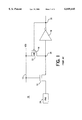
Pass transistors have been designed to handle overvoltage conditions and to protect receiver circuits. Such a circuit is shown in FIG. 1. As shown, prior art circuit 10 comprises pass transistor 14, which is an n-channel MOSFET, connected between pad 24 and receiver 18. The gate of pass transistor 14 is coupled to supply voltage 12, VDD. Receiver 18 also has the drain of keeper MOSFET 16, which is a p-channel MOSFET, connected to its input node 26. Output node 20 of receiver 18 is coupled to the gate of keeper MOSFET 16. The source of keeper MOSFET 16 is coupled to supply voltage 12. To those familiar with the art, keeper MOSFET 16 may also be referred to as a boost transistor or half-latch transistor.
Generally, a high signal voltage level is at about VDD and a low signal voltage level is at about VSS, or ground. In normal operation, when supply voltage VDD is "on," a high signal voltage level at pad 24 generates a "weak" high at node 26. The "weak" high is caused by the threshold voltage drop across the input and output sides of pass transistor 14. The voltage level may be brought back up to VDD at node 26 by keeper MOSFET 16. A low signal level at node 20 turns on p-channel MOSFET 16, which then latches node 26 to VDD. Consequently, any overvoltage condition at pad 24 is absorbed by the threshold voltage drop across the pass transistor 14.
Because node 26 is latched to VDD when MOSFET 16 is on, an overvoltage condition or an ESD condition at pad 24 stresses pass transistor 14. Furthermore, an ESD condition at pad 24 stresses pass transistor 14 even when MOSFET 16 is off. During its off state, n-well 22 is at VDD potential and the drain of MOSFET 16 at node 26 is at a single diode voltage drop away from VDD. When node 26 rises one diode voltage drop above n-well 22, node 26 is effectively pinned to a voltage potential of VDD plus one diode voltage drop. The pinning of node 26 stresses pass transistor 14 during an overvoltage or ESD condition at pad 24.
Stress problems potentially exist even when the circuit of FIG. 1 is unpowered. If VDD is at ground potential, node 26 is pinned, nevertheless, to a voltage potential of one divide voltage drop above ground potential. Again, an ESD condition at pad 24 may stress pass transistor 14. From the above discussion, it is seen that an improved receiver circuit that is tolerant to overvoltage and ESD conditions is needed.
SUMMARY OF THE INVENTION
To meet this and other needs, and in view of its purposes, the present invention provides a receiver circuit that is substantially insensitive to overvoltage and ESD conditions. In one embodiment, the receiver circuit includes a pass transistor having an input side for receiving a signal, an output side, and a gate susceptible to damage when an ESD potential is present. A receiver is coupled to the output side of the pass transistor to receive the signal. A first protection circuit has a first rail, providing an operating voltage potential to the gate of the pass transistor, and structure that electrically decouples the first rail from the gate of the pass transistor. The first protection circuit provides (1) the operating voltage potential to the gate when an ESD potential is not present, and (2) a voltage which tracks the ESD potential when the ESD potential is present at the input side of the pass transistor.
The receiver circuit also may include a second protection circuit having a first mechanism for providing a test signal voltage to the output side of the pass transistor and a second mechanism for electrically decoupling the output side of the pass transistor from the test signal voltage. The second protection circuit provides (1) the test signal voltage to the output side of the pass transistor when an ESD potential is not present, and (2) a voltage which tracks the ESD potential when the ESD potential is present at the input side of the pass transistor. A resistor and a clamping transistor may also be added to the receiver circuit to provide additional robust structure guarding against overvoltage or ESD conditions.
It is understood that the foregoing general description and the following detailed description are exemplary, but are not restrictive, of the invention.
BRIEF DESCRIPTION OF THE DRAWING
The invention is best understood from the following detailed description when read in connection with the accompanying drawing. Included in the drawing are the following figures:
FIG. 1 is a schematic diagram of a prior art receiver circuit;
FIG. 2 is a schematic diagram of a receiver circuit according to a first embodiment of the present invention; and
FIG. 3 is a schematic diagram of a further embodiment of the present invention.
DETAILED DESCRIPTION OF THE INVENTION
FIG. 2 is a circuit diagram of a first embodiment of a receiver circuit according to the present invention. As shown, receiver circuit 30 comprises pass transistor 58 connected between pad 56 and receiver 62. Receiver 62 has an input at node 60 and an output at node 64. The gate of pass transistor 58 is serviced by first protection circuit 31, which provides a voltage-tolerant voltage divider network; protection circuit 31 is comprised of three p-channel MOSFETs, namely MOSFET 34, MOSFET 36, and MOSFET 42. As explained below, MOSFETs 36 and 42 are voltage dividers which provide a potential V* at first rail 38.
The voltage dividers are coupled between second rail 32, which provides VCC potential, and third rail 44, which provides VSS potential. MOSFET 34 is a well bias controller for the voltage dividers. The drain of MOSFET 34 is connected through node 40 to the n-wells of all the MOSFETs in first protection circuit 31, namely MOSFETs 34, 36, and 42.
Also shown in FIG. 2 is second protection circuit 33 which is comprised of two p-channel MOSFETs, namely MOSFET 48 and MOSFET 52. As explained below, MOSFET 52 provides an Iddq test function and MOSFET 48 is a second well bias controller. It will be appreciated that MOSFET 52 may provide a different switching function; for exemplary purpose, however, MOSFET 48 provides the Iddq test function. The source of each MOSFET 48 and 52 is connected to a fourth rail 46, which provides VDD potential. The gate of MOSFET 52 is connected to test pin 54 for receiving the Iddq test enable signal. Finally, the gate of MOSFET 48 is connected to node 60, the input to receiver 62; the drain of MOSFET 48 is connected to the n-wells of MOSFETs 48 and 52 at node 50.
The operation of first protection circuit 31 will now be explained. During normal operation, second rail 32 is at VCC potential and third rail 44 is at VSS potential. VSS potential is lower then VCC, and may be at ground potential. MOSFETs 36 and 42 are coupled between the second rail 32 and third rail 44.
Due to the voltage divider actions of MOSFETs 36 and 42, V* is at a lower potential than VCC and at a higher potential than VSS. Because the gate of MOSFET 34 is at V* potential and the source of MOSFET 34 is at the higher potential of VCC, p-channel MOSFET 34 is also on. Consequently, the drain of MOSFET 34 is near the potential of VCC. The n-wells are also at the potential of VCC, and forward biasing of these transistors does not occur, because the n-wells of p- channel MOSFETs 34, 36, and 42 are connected to the drain of MOSFET 34.
Next the operation of first protection circuit 31 is explained during an unpowered condition of receiver circuit 30, and during an overvoltage of an ESD environment. As will be appreciated by those skilled in the art, when an overvoltage or ESD occurs at pad 56, the gate of pass transistor 58, an n-channel MOSFET, may rise to a high potential. The cause of such high potential is a large parasitic capacitance that exists between the input side of pass transistor 58 and the gate of pass transistor 58. As the gate of pass transistor 58 rises, the source of MOSFET 42 also rises and the n-well of MOSFET 42 also rises to one diode voltage drop relative to its source.
Assuming that second rail 32 is at a ground potential, MOSFETs 34 and 36 are both off as the potential of first rail 38 rises, and the n-wells of MOSFETs 34 and 36 rise to the same potential as the n-well of MOSFET 42. Thus, all the n-wells in first protection circuit 31 track the potential of first rail 38. Furthermore, because first well bias controller or MOSFET 34 is off when the potential of first rail 38 rises, the n-wells are permitted to track the potential of first rail 38. When the n-wells track the potential of the first rail 38, the diodes in MOSFETs 36 and 42 do not turn on at all and, consequently, the potential of the n-wells moves with the potential of first rail 38.
In summary, in accordance with one embodiment of the present invention, first well bias controller (MOSFET 34) decouples the n-well node from second rail 32, allowing the n-well node to float. Because the n-well node floats, there is no continuous current flow out of first rail 38 and the potential of the gate of pass transistor 58 moves or tracks with input pad 56. Consequently, the dielectric voltage stress on pass transistor 58 is reduced.
Turning next to second protection circuit 33, its operation will now be explained. During test operation of receiver circuit 30, the Iddq test enable signal is provided to test pin 54, which places the gate of the Iddq test function transistor (MOSFET 52) at a ground potential. Because the source of MOSFET 52 is at the higher potential of VDD, MOSFET 52 is on and its drain voltage at node 60 at VDD. In addition, because the gate of the second well bias controller (MOSFET 48) has a lower potential than fourth rail 46, the bias controller is on. This condition forces the n-wells of MOSFETs 48 and 52 to rise to VDD. In situations when the gate of MOSFET 48 is at a higher potential than VDD, MOSFET 48 turns off and the n-wells of MOSFETs 48 and 52 track node 60 to within one diode voltage drop.
In the case of an unpowered condition of receiver circuit 30 and an ESD potential placed on pad 56, fourth rail 46 may be at a ground potential and node 60 may start rising. MOSFET 48 is off in this circumstance, and the potential of the n-wells of MOSFETs 48 and 52 rise together with the potential of node 60. Consequently, the pinning of node 60 is prevented, reducing the dielectric voltage stress across pass transistor 58.
In summary, in accordance with another aspect of the present invention, second well bias controller (MOSFET 48) decouples the n-well node from fourth rail 46, allowing the n-well node to float. In this manner, node 60 may also float and move with any overvoltage or ESD potential preset on the output side of pass transistor 58, due to voltage punch-through or snap-back conditions in pass transistor 58.
FIG. 3 shows another embodiment of the present invention. Shown is receiver circuit 70, which has first protection circuit 31 and second protection circuit 33 each of which is similar to the respective protection circuits shown in FIG. 2. (Like reference numerals refer to like elements throughout the drawing.) Added to resistor circuit 70 in FIG. 2 is a resistor 72 and an n-channel MOSFET 74 connected in series between the output of pass transistor 58 and the input side of receiver 62, at node 60. N-channel MOSFET 74 is connected between node 60 and ground terminal 76. The gate of MOSFET 74 is also connected to ground terminal 76.
It will be appreciated that resistor 72 and MOSFET 74 provide additional robust structure guarding against overvoltage or ESD conditions at pad 56. Any rise in potential at the output side of pass transistor 58, resulting from an overvoltage or ESD condition at pad 56, may be dissipated to ground across resistor 72 and MOSFET 74. It will further be appreciated that MOSFET 74 is an overvoltage clamp. It dynamically clamps node 60 to a fixed voltage level above ground potential. The fixed voltage level is the MOSFET snap-back voltage or punch-through voltage of MOSFET 74.
Although illustrated and described herein with reference to certain specific embodiments, the present invention is nevertheless not intended to be limited to the details shown. Rather, various modifications may be made in the details within the scope and range of equivalents of the claims and without departing from the spirit of the invention. It will be understood, for example, that the present invention is not limited to only the receiver single circuit described herein. Rather, the invention may be extended to other types of receivers, such as differential receivers.

Claims (19)

What is claimed:
1. A receiver circuit in an electrostatic discharge (ESD) environment comprising:
a pass transistor having an input side receiving a signal, an output side, and a gate susceptible to damage when an ESD potential is present;
a protection circuit having:
(a) a first rail providing an operating voltage potential to the gate of the pass transistor;
(b) a second rail providing VCC voltage potential;
(c) a third rail providing VSS voltage potential; and
(d) means for electrically decoupling the first rail from the second rail and the third rail;
wherein the protection circuit provides (1) the operating voltage potential to the gate when an ESD potential is not present, and (2) a voltage which tracks the ESD potential when the ESD potential is present at the input side of the pass transistor.
2. The receiver circuit of claim 1 wherein the protection circuit further has:
a voltage divider providing the operating voltage potential and being coupled between the second rail and the third rail; and
a first well bias controller coupled between the voltage divider and the first rail for adjusting the potential of the first rail when the ESD potential is present.
3. The receiver circuit of claim 2 further comprising a first node and wherein:
the voltage divider further includes:
(a) a first p-channel MOSFET having a source connected to the second rail, a drain connected to the first rail, a gate connected to the first rail, and an n-well connected to the first node, and
(b) a second p-channel MOSFET having a source connected to the first rail, a drain and a gate connected to the third rail, and an n-well connected to the first node; and
the first well bias controller further includes a third p-channel MOSFET having a drain and an n-well connected to the first node, a source connected to the second rail, and a gate connected to the first rail.
4. The receiver circuit of claim 3 wherein the third p-channel MOSFET is on when the operating voltage potential is provided to the gate of the pass transistor and is off when the ESD potential is above the operating voltage potential.
5. The receiver circuit of claim 4 wherein the first node tracks the voltage potential on the first rail.
6. The receiver circuit of claim 5 wherein the pass transistor is an n-channel MOSFET.
7. A receiver circuit in an electrostatic discharge (ESD) environment comprising:
a pass transistor having an input side receiving a signal and an output side, the pass transistor susceptible to damage when an excessive potential is present across the input and output sides;
a receiver coupled to the output side of the pass transistor for receiving the signal;
a protection circuit having:
(a) test enable means for providing a test signal voltage to the output side of the pass transistor, and
(b) means for electrically decoupling the output side of the pass transistor;
wherein the protection circuit provides (1) the test signal voltage to the output side of the pass transistor when an ESD potential is not present, and (2) a voltage which tracks the ESD potential when the ESD potential is present at the input side of the pass transistor.
8. The receiver circuit of claim 7 further comprising a rail providing VDD voltage potential and wherein the test enable means further includes:
a first p-channel MOSFET coupled between the rail and the output side of the pass transistor; and
a well bias controller coupled between the first p-channel MOSFET and the output side of the pass transistor for adjusting the potential of the output side of the pass transistor when the ESD potential is present.
9. The receiver circuit of claim 8 further comprising a test pin and a node and wherein:
the first p-channel MOSFET has a source connected to the rail, a drain connected to the output side of the pass transistor, a gate connected to the test pin for providing a test enable signal, and an n-well connected to the node; and
the well bias controller includes a second p-channel MOSFET having a source connected to the rail, a gate connected to the output side of the pass transistor, and a drain and an n-well connected to the node.
10. The receiver circuit of claim 9 wherein the first p-channel MOSFET is on when a voltage potential at the output side of the pass transistor is below VDD and off when the voltage potential at the output side of the pass transistor is above VDD.
11. The receiver circuit of claim 10 wherein the node tracks the voltage potential on the output side of the pass transistor.
12. The receiver circuit of claim 11 wherein the pass transistor is an n-channel MOSFET.
13. The receiver circuit of claim 12 further comprising:
a ground terminal;
a resistor connected between the gate of the second p-channel MOSFET and the drain of the first p-channel MOSFET; and
a clamping transistor connected between the drain of the first p-channel MOSFET and the ground terminal.
14. The receiver circuit of claim 13 wherein the clamping transistor is an n-channel MOSFET having a gate and a source connected to the ground terminal and a drain connected to the drain of the first p-channel MOSFET.
15. A receiver circuit in an electrostatic discharge (ESD) environment comprising:
a pass transistor having an input side receiving a signal, an output side, and a gate, the pass transistor susceptible to damage when an ESD potential is present;
a receiver coupled to the output side of the pass transistor for receiving the signal;
a first protection circuit having (a) a first rail providing an operating voltage potential to the gate of the pass transistor, and (b) means for electrically decoupling the first rail from the gate of the pass transistor;
a second protection circuit having (a) test enable means for providing a test signal voltage to the output side of the pass transistor, and (b) means for electrically decoupling the output side of the pass transistor;
wherein the first protection circuit provides (1) the operating voltage potential to the gate when an ESD potential is not present, and (2) a voltage which tracks the ESD potential when the ESD potential is present at the input side of the pass transistor; and
the second protection circuit provides (1) the test signal voltage to the output side of the pass transistor when an ESD potential is not present, and (2) a voltage which tracks the ESD potential when the ESD potential is present at the input side of the pass transistor.
16. The receiver circuit of claim 15 wherein:
the first protection circuit includes:
(a) a second rail and a third rail,
(b) a first node,
(c) a first p-channel MOSFET having a source connected to the second rail, a drain connected to the first rail, a gate connected to the first rail, and an n-well connected to the first node,
(d) a second p-channel MOSFET having a source connected to the first rail, a drain and a gate connected to the third rail, and an n-well connected to the first node, and
(e) a third p-channel MOSFET having a drain and an n-well connected to the first node, a source connected to the second rail, and a gate connected to the first rail; and
the second protection circuit includes:
(f) a fourth rail,
(g) a test pin providing a test enable signal,
(h) a second node,
(i) a fourth p-channel MOSFET having a source connected to the fourth rail, a drain connected to the output side of the pass transistor, a gate connected to the test pin, and an n-well connected to the second node, and
(j) a fifth p-channel MOSFET having a source connected to the fourth rail, a gate connected to the output side of the pass transistor, and a drain and an n-well connected to the second node.
17. The receiver circuit of claim 16 wherein the pass transistor is an n-channel MOSFET.
18. The receiver circuit of claim 17 further comprising:
a ground terminal;
a resistor connected between the gate of the fifth p-channel MOSFET and the drain of the fourth p-channel MOSFET; and
a clamping transistor connected between the drain of the fourth p-channel MOSFET and the ground terminal.
19. The receiver circuit of claim 18 wherein the clamping transistor is an n-channel MOSFET having a gate and a source connected to the ground terminal and a drain connected to the drain of the fourth p-channel MOSFET.
US09/156,111 1998-09-18 1998-09-18 Overvoltage and electrostatic discharge protection for a receiver circuit Expired - Lifetime US6049445A (en)

Priority Applications (1)

Application Number Priority Date Filing Date Title
US09/156,111 US6049445A (en) 1998-09-18 1998-09-18 Overvoltage and electrostatic discharge protection for a receiver circuit

Applications Claiming Priority (1)

Application Number Priority Date Filing Date Title
US09/156,111 US6049445A (en) 1998-09-18 1998-09-18 Overvoltage and electrostatic discharge protection for a receiver circuit

Publications (1)

Publication Number Publication Date
US6049445A true US6049445A (en) 2000-04-11

Family

ID=22558141

Family Applications (1)

Application Number Title Priority Date Filing Date
US09/156,111 Expired - Lifetime US6049445A (en) 1998-09-18 1998-09-18 Overvoltage and electrostatic discharge protection for a receiver circuit

Country Status (1)

Country Link
US (1) US6049445A (en)

Cited By (16)

* Cited by examiner, † Cited by third party
Publication number Priority date Publication date Assignee Title
US6362653B1 (en) 2001-02-06 2002-03-26 International Business Machines Corporation High voltage tolerant receivers
US6400546B1 (en) * 1999-09-02 2002-06-04 Ati International Srl I/O pad voltage protection circuit and method
US6441670B1 (en) 2001-08-15 2002-08-27 International Business Machines Corporation 5V-tolerant receiver for low voltage CMOS technologies
US20040021997A1 (en) * 2002-07-30 2004-02-05 Chartered Semiconductor Manufacturing Ltd. Novel ESD protection circuit for I/O circuitry
US6768618B1 (en) * 2002-08-01 2004-07-27 Cypress Semiconductor, Corp. Input gate protection circuit and method
US6798629B1 (en) * 2001-06-15 2004-09-28 Integrated Device Technology, Inc. Overvoltage protection circuits that utilize capacitively bootstrapped variable voltages
US20080150624A1 (en) * 2006-12-22 2008-06-26 Taylor Stewart S Vgs replication apparatus, method, and system
US20080158757A1 (en) * 2007-01-02 2008-07-03 Freescale Semiconductor, Inc. Short circuit and over-voltage protection for a data bus
US20100176848A1 (en) * 2008-07-17 2010-07-15 Ati Technologies Ulc Input/output buffer circuit
US20100219855A1 (en) * 2009-02-03 2010-09-02 Nec Electronics Corporation Semiconductor device having CMOS transfer circuit and clamp element
US20110102055A1 (en) * 2009-11-05 2011-05-05 Honeywell International Inc. Low-side driver high-voltage transient protection circuit
US20120007636A1 (en) * 2007-10-30 2012-01-12 Rohm Co., Ltd. Analog switch for signal swinging between positive and negative voltages
US8847657B2 (en) * 2012-06-22 2014-09-30 Avago Technologies General Ip (Singapore) Pte. Ltd. Low power receiver for implementing a high voltage interface implemented with low voltage devices
US20160149486A1 (en) * 2014-11-26 2016-05-26 Taiwan Semiconductor Manufacturing Company, Ltd. Input-output circuits
CN109039328A (en) * 2014-06-30 2018-12-18 意法半导体研发(深圳)有限公司 The drive circuit with grid clamping of support pressure test
US11038345B2 (en) * 2019-03-25 2021-06-15 Nxp B.V. Over-voltage tolerant analog test bus

Citations (10)

* Cited by examiner, † Cited by third party
Publication number Priority date Publication date Assignee Title
US4922371A (en) * 1988-11-01 1990-05-01 Teledyne Semiconductor ESD protection circuit for MOS integrated circuits
US4937700A (en) * 1988-01-07 1990-06-26 Kabushiki Kaisha Toshiba Semiconductor integrated circuit with a circuit limiting an input voltage to a predetermined voltage
US5333093A (en) * 1991-11-06 1994-07-26 Siemens Aktiengesellschaft Protection apparatus for series pass MOSFETS
US5576635A (en) * 1995-02-14 1996-11-19 Advanced Micro Devices, Inc. Output buffer with improved tolerance to overvoltage
US5591992A (en) * 1991-03-28 1997-01-07 Texas Instruments Incorporated Electrostatic discharge protection in integrated circuits, systems and methods
US5784242A (en) * 1994-08-29 1998-07-21 Cypress Semiconductor Corp. Apparatus for smart power supply ESD protection structure
US5793592A (en) * 1997-05-13 1998-08-11 International Business Machines Corporation Dynamic dielectric protection circuit for a receiver
US5815354A (en) * 1997-03-21 1998-09-29 International Business Machines Corporation Receiver input voltage protection circuit
US5852540A (en) * 1997-09-24 1998-12-22 Intel Corporation Circuit for protecting the input/output stage of a low voltage integrated circuit device from a failure of the internal voltage supply or a difference in the power-up sequencing of supply voltage levels
US5859442A (en) * 1996-12-03 1999-01-12 Micron Technology, Inc. Circuit and method for configuring a redundant bond pad for probing a semiconductor

Patent Citations (11)

* Cited by examiner, † Cited by third party
Publication number Priority date Publication date Assignee Title
US4937700A (en) * 1988-01-07 1990-06-26 Kabushiki Kaisha Toshiba Semiconductor integrated circuit with a circuit limiting an input voltage to a predetermined voltage
US4922371A (en) * 1988-11-01 1990-05-01 Teledyne Semiconductor ESD protection circuit for MOS integrated circuits
US5591992A (en) * 1991-03-28 1997-01-07 Texas Instruments Incorporated Electrostatic discharge protection in integrated circuits, systems and methods
US5637892A (en) * 1991-03-28 1997-06-10 Texas Instruments Incorporated Electrostatic discharge protection in integrated circuits, systems and methods
US5333093A (en) * 1991-11-06 1994-07-26 Siemens Aktiengesellschaft Protection apparatus for series pass MOSFETS
US5784242A (en) * 1994-08-29 1998-07-21 Cypress Semiconductor Corp. Apparatus for smart power supply ESD protection structure
US5576635A (en) * 1995-02-14 1996-11-19 Advanced Micro Devices, Inc. Output buffer with improved tolerance to overvoltage
US5859442A (en) * 1996-12-03 1999-01-12 Micron Technology, Inc. Circuit and method for configuring a redundant bond pad for probing a semiconductor
US5815354A (en) * 1997-03-21 1998-09-29 International Business Machines Corporation Receiver input voltage protection circuit
US5793592A (en) * 1997-05-13 1998-08-11 International Business Machines Corporation Dynamic dielectric protection circuit for a receiver
US5852540A (en) * 1997-09-24 1998-12-22 Intel Corporation Circuit for protecting the input/output stage of a low voltage integrated circuit device from a failure of the internal voltage supply or a difference in the power-up sequencing of supply voltage levels

Cited By (26)

* Cited by examiner, † Cited by third party
Publication number Priority date Publication date Assignee Title
US6400546B1 (en) * 1999-09-02 2002-06-04 Ati International Srl I/O pad voltage protection circuit and method
US6362653B1 (en) 2001-02-06 2002-03-26 International Business Machines Corporation High voltage tolerant receivers
US6798629B1 (en) * 2001-06-15 2004-09-28 Integrated Device Technology, Inc. Overvoltage protection circuits that utilize capacitively bootstrapped variable voltages
US6441670B1 (en) 2001-08-15 2002-08-27 International Business Machines Corporation 5V-tolerant receiver for low voltage CMOS technologies
US20040021997A1 (en) * 2002-07-30 2004-02-05 Chartered Semiconductor Manufacturing Ltd. Novel ESD protection circuit for I/O circuitry
US6768618B1 (en) * 2002-08-01 2004-07-27 Cypress Semiconductor, Corp. Input gate protection circuit and method
US20080150624A1 (en) * 2006-12-22 2008-06-26 Taylor Stewart S Vgs replication apparatus, method, and system
US7676213B2 (en) * 2006-12-22 2010-03-09 Taylor Stewart S Vgs replication apparatus, method, and system
US20080158757A1 (en) * 2007-01-02 2008-07-03 Freescale Semiconductor, Inc. Short circuit and over-voltage protection for a data bus
US7835124B2 (en) * 2007-01-02 2010-11-16 Freescale Semiconductor, Inc. Short circuit and over-voltage protection for a data bus
US8149042B2 (en) * 2007-10-30 2012-04-03 Rohm Co., Ltd. Analog switch for signal swinging between positive and negative voltages
US20120007636A1 (en) * 2007-10-30 2012-01-12 Rohm Co., Ltd. Analog switch for signal swinging between positive and negative voltages
US20100176848A1 (en) * 2008-07-17 2010-07-15 Ati Technologies Ulc Input/output buffer circuit
US8344760B2 (en) 2008-07-17 2013-01-01 Ati Technologies Ulc Input/output buffer circuit
US8564318B2 (en) 2009-02-03 2013-10-22 Renesas Electronics Corporation Semiconductor device having CMOS transfer circuit and clamp element
US8421489B2 (en) * 2009-02-03 2013-04-16 Renesas Electronics Corporation Semiconductor device having CMOS transfer circuit and clamp element
US20100219855A1 (en) * 2009-02-03 2010-09-02 Nec Electronics Corporation Semiconductor device having CMOS transfer circuit and clamp element
US8339181B2 (en) 2009-11-05 2012-12-25 Honeywell International Inc. Low-side driver high-voltage transient protection circuit
US20110102055A1 (en) * 2009-11-05 2011-05-05 Honeywell International Inc. Low-side driver high-voltage transient protection circuit
US8847657B2 (en) * 2012-06-22 2014-09-30 Avago Technologies General Ip (Singapore) Pte. Ltd. Low power receiver for implementing a high voltage interface implemented with low voltage devices
CN109039328A (en) * 2014-06-30 2018-12-18 意法半导体研发(深圳)有限公司 The drive circuit with grid clamping of support pressure test
CN109039328B (en) * 2014-06-30 2022-08-26 意法半导体研发(深圳)有限公司 Driver circuit with gate clamp supporting stress test
US20160149486A1 (en) * 2014-11-26 2016-05-26 Taiwan Semiconductor Manufacturing Company, Ltd. Input-output circuits
US9780647B2 (en) * 2014-11-26 2017-10-03 Taiwan Semiconductor Manufacturing Company, Ltd. Input-output circuits
US10186958B2 (en) 2014-11-26 2019-01-22 Taiwan Semiconductor Manufacturing Company, Ltd. Input-output circuits
US11038345B2 (en) * 2019-03-25 2021-06-15 Nxp B.V. Over-voltage tolerant analog test bus

Similar Documents

Publication Publication Date Title
EP0042305B1 (en) Mos transistor circuit with breakdown protection
US6049445A (en) Overvoltage and electrostatic discharge protection for a receiver circuit
EP0575062B1 (en) ESD protection of output buffers
US6970336B2 (en) Electrostatic discharge protection circuit and method of operation
US6515534B2 (en) Enhanced conductivity body biased PMOS driver
KR100295316B1 (en) Low voltage input and output circuit with overvoltage protection
US7138847B2 (en) Sub-micron high input voltage tolerant input output (I/O) circuit which accommodates large power supply variations
JP3926975B2 (en) Stacked MOS transistor protection circuit
US5946175A (en) Secondary ESD/EOS protection circuit
US6867461B1 (en) ESD protection circuit
US6867957B1 (en) Stacked-NMOS-triggered SCR device for ESD-protection
US7304827B2 (en) ESD protection circuits for mixed-voltage buffers
US7710695B2 (en) Integrated circuit and electrostatic discharge protection circuit
US6552583B1 (en) ESD-protection device with active R-C coupling to gate of large output transistor
US7339771B2 (en) Electrostatic protection circuit
US5894230A (en) Modified keeper half-latch receiver circuit
US6492686B1 (en) Integrated circuit having buffering circuitry with slew rate control
US20060198069A1 (en) Power ESD clamp protection circuit
US6292046B1 (en) CMOS electrostatic discharge protection circuit with minimal loading for high speed circuit applications
US6380570B1 (en) Gate overvoltage control networks
US20030122606A1 (en) Hot carrier injection suppression circuit
US6818953B2 (en) Protection of an integrated circuit against electrostatic discharges and other overvoltages
US20050127444A1 (en) Semiconductor integrated circuit
US11811221B2 (en) Electrostatic discharge protection device
US20240088650A1 (en) Circuit and method for high voltage tolerant esd protection

Legal Events

Date Code Title Description
AS Assignment

Owner name: INTERNATIONAL BUSINESS MACHINES CORPORATION, NEW Y

Free format text: ASSIGNMENT OF ASSIGNORS INTEREST;ASSIGNORS:GAUTHIER, ROBERT J., JR.;VOLDMAN, STEVEN H.;REEL/FRAME:009475/0353

Effective date: 19980909

STCF Information on status: patent grant

Free format text: PATENTED CASE

FEPP Fee payment procedure

Free format text: PAYOR NUMBER ASSIGNED (ORIGINAL EVENT CODE: ASPN); ENTITY STATUS OF PATENT OWNER: LARGE ENTITY

FPAY Fee payment

Year of fee payment: 4

FPAY Fee payment

Year of fee payment: 8

FPAY Fee payment

Year of fee payment: 12