US6050739A - Robot end effector for automated wet wafer processing - Google Patents
Robot end effector for automated wet wafer processing Download PDFInfo
- Publication number
- US6050739A US6050739A US08/980,702 US98070297A US6050739A US 6050739 A US6050739 A US 6050739A US 98070297 A US98070297 A US 98070297A US 6050739 A US6050739 A US 6050739A
- Authority
- US
- United States
- Prior art keywords
- finger
- arm
- robot
- end effector
- length
- Prior art date
- Legal status (The legal status is an assumption and is not a legal conclusion. Google has not performed a legal analysis and makes no representation as to the accuracy of the status listed.)
- Expired - Fee Related
Links
- 239000012636 effector Substances 0.000 title claims abstract description 47
- 238000012545 processing Methods 0.000 title claims abstract description 21
- 238000000034 method Methods 0.000 claims description 10
- 238000004140 cleaning Methods 0.000 claims description 4
- 238000005260 corrosion Methods 0.000 claims description 3
- 230000007797 corrosion Effects 0.000 claims description 3
- NBVXSUQYWXRMNV-UHFFFAOYSA-N fluoromethane Chemical compound FC NBVXSUQYWXRMNV-UHFFFAOYSA-N 0.000 claims description 2
- 238000012423 maintenance Methods 0.000 abstract description 10
- 239000000126 substance Substances 0.000 abstract description 6
- 235000012431 wafers Nutrition 0.000 description 36
- 239000004065 semiconductor Substances 0.000 description 6
- 239000000463 material Substances 0.000 description 3
- 239000011248 coating agent Substances 0.000 description 2
- 238000000576 coating method Methods 0.000 description 2
- 238000005530 etching Methods 0.000 description 2
- 238000004519 manufacturing process Methods 0.000 description 2
- 238000012986 modification Methods 0.000 description 2
- 230000004048 modification Effects 0.000 description 2
- 238000012546 transfer Methods 0.000 description 2
- XUIMIQQOPSSXEZ-UHFFFAOYSA-N Silicon Chemical compound [Si] XUIMIQQOPSSXEZ-UHFFFAOYSA-N 0.000 description 1
- 239000000969 carrier Substances 0.000 description 1
- 239000003518 caustics Substances 0.000 description 1
- 230000000694 effects Effects 0.000 description 1
- 238000003754 machining Methods 0.000 description 1
- 239000002184 metal Substances 0.000 description 1
- 229910052710 silicon Inorganic materials 0.000 description 1
- 239000010703 silicon Substances 0.000 description 1
- 229910001220 stainless steel Inorganic materials 0.000 description 1
- 239000010935 stainless steel Substances 0.000 description 1
- 238000011282 treatment Methods 0.000 description 1
Images


Classifications
-
- H—ELECTRICITY
- H01—ELECTRIC ELEMENTS
- H01L—SEMICONDUCTOR DEVICES NOT COVERED BY CLASS H10
- H01L21/00—Processes or apparatus adapted for the manufacture or treatment of semiconductor or solid state devices or of parts thereof
- H01L21/67—Apparatus specially adapted for handling semiconductor or electric solid state devices during manufacture or treatment thereof; Apparatus specially adapted for handling wafers during manufacture or treatment of semiconductor or electric solid state devices or components ; Apparatus not specifically provided for elsewhere
- H01L21/683—Apparatus specially adapted for handling semiconductor or electric solid state devices during manufacture or treatment thereof; Apparatus specially adapted for handling wafers during manufacture or treatment of semiconductor or electric solid state devices or components ; Apparatus not specifically provided for elsewhere for supporting or gripping
- H01L21/687—Apparatus specially adapted for handling semiconductor or electric solid state devices during manufacture or treatment thereof; Apparatus specially adapted for handling wafers during manufacture or treatment of semiconductor or electric solid state devices or components ; Apparatus not specifically provided for elsewhere for supporting or gripping using mechanical means, e.g. chucks, clamps or pinches
- H01L21/68707—Apparatus specially adapted for handling semiconductor or electric solid state devices during manufacture or treatment thereof; Apparatus specially adapted for handling wafers during manufacture or treatment of semiconductor or electric solid state devices or components ; Apparatus not specifically provided for elsewhere for supporting or gripping using mechanical means, e.g. chucks, clamps or pinches the wafers being placed on a robot blade, or gripped by a gripper for conveyance
-
- F—MECHANICAL ENGINEERING; LIGHTING; HEATING; WEAPONS; BLASTING
- F16—ENGINEERING ELEMENTS AND UNITS; GENERAL MEASURES FOR PRODUCING AND MAINTAINING EFFECTIVE FUNCTIONING OF MACHINES OR INSTALLATIONS; THERMAL INSULATION IN GENERAL
- F16B—DEVICES FOR FASTENING OR SECURING CONSTRUCTIONAL ELEMENTS OR MACHINE PARTS TOGETHER, e.g. NAILS, BOLTS, CIRCLIPS, CLAMPS, CLIPS OR WEDGES; JOINTS OR JOINTING
- F16B2200/00—Constructional details of connections not covered for in other groups of this subclass
- F16B2200/40—Clamping arrangements where clamping parts are received in recesses of elements to be connected
- F16B2200/403—Threaded clamping parts
-
- Y—GENERAL TAGGING OF NEW TECHNOLOGICAL DEVELOPMENTS; GENERAL TAGGING OF CROSS-SECTIONAL TECHNOLOGIES SPANNING OVER SEVERAL SECTIONS OF THE IPC; TECHNICAL SUBJECTS COVERED BY FORMER USPC CROSS-REFERENCE ART COLLECTIONS [XRACs] AND DIGESTS
- Y10—TECHNICAL SUBJECTS COVERED BY FORMER USPC
- Y10S—TECHNICAL SUBJECTS COVERED BY FORMER USPC CROSS-REFERENCE ART COLLECTIONS [XRACs] AND DIGESTS
- Y10S414/00—Material or article handling
- Y10S414/135—Associated with semiconductor wafer handling
- Y10S414/141—Associated with semiconductor wafer handling includes means for gripping wafer
-
- Y—GENERAL TAGGING OF NEW TECHNOLOGICAL DEVELOPMENTS; GENERAL TAGGING OF CROSS-SECTIONAL TECHNOLOGIES SPANNING OVER SEVERAL SECTIONS OF THE IPC; TECHNICAL SUBJECTS COVERED BY FORMER USPC CROSS-REFERENCE ART COLLECTIONS [XRACs] AND DIGESTS
- Y10—TECHNICAL SUBJECTS COVERED BY FORMER USPC
- Y10T—TECHNICAL SUBJECTS COVERED BY FORMER US CLASSIFICATION
- Y10T403/00—Joints and connections
- Y10T403/46—Rod end to transverse side of member
-
- Y—GENERAL TAGGING OF NEW TECHNOLOGICAL DEVELOPMENTS; GENERAL TAGGING OF CROSS-SECTIONAL TECHNOLOGIES SPANNING OVER SEVERAL SECTIONS OF THE IPC; TECHNICAL SUBJECTS COVERED BY FORMER USPC CROSS-REFERENCE ART COLLECTIONS [XRACs] AND DIGESTS
- Y10—TECHNICAL SUBJECTS COVERED BY FORMER USPC
- Y10T—TECHNICAL SUBJECTS COVERED BY FORMER US CLASSIFICATION
- Y10T74/00—Machine element or mechanism
- Y10T74/20—Control lever and linkage systems
- Y10T74/20207—Multiple controlling elements for single controlled element
- Y10T74/20305—Robotic arm
Definitions
- This invention relates generally to robots used in semiconductor processing and particularly to robots used for wet wafer processing.
- Semiconductor wafers may be processed in a variety of wet steps to effect cleaning, etching, stripping, coating and other results. Often the chemicals may be caustic or corrosive.
- Robots may be utilized to transfer the wafers between various stations and to physically process those wafers at a particular station.
- the robots under computer control, allow the wafer fabrication process to be accurately controlled by computer and it is possible to know at every stage where a given wafer is in the process.
- the robot can handle heavy wafer batches.
- the robot In conventional robotic wet wafer processing operations, the robot includes an arm or end effector which is adapted with fingers.
- the end effector adapts the robot to semiconductor processing.
- the disc-shaped silicon wafers are somewhat delicate to handle and must be treated with care to avoid damaging the wafers.
- the wafers are conventionally carried in a carrier with a handle. A number of wafers may be held on edge in the carrier so that all of the wafers in the carrier will receive, at least so long as they are in the same carrier, the same wafer processing.
- the wafer fabrication process can be automated, achieving many of the advantages described above.
- the robot arm carrying the carrier also be exposed to many of the chemical conditions that the wafers themselves are exposed to in the normal course of operation of the robot.
- the end effectors may be covered by a material that can withstand high temperature, corrosive conditions. If that covering material is scratched, the underlying metal may be subject to corrosive attack. This may require repair of the end effector. This repair may involve re-machining and re-coating.
- the arms must be precisely attached to the robot. This is because the robot is programmed to move the arm through desired patterns, assuming the arm is oriented as it was when the arm motion was programmed. Since the orientation of the arm on the robot is adjustable, repositioning the arm after maintenance can be a painstaking process.
- a robot end effector for automated processing facilitates wet wafer processing by improving the maintenance of the end effector.
- the end effector may be exposed to a variety of chemical conditions in the course of its operation.
- the end effector finger By making the end effector finger removable from the arm, maintenance of the end effector finger is facilitated.
- a wet wafer processing robot includes an arm having an end effector finger adapted to engage a wafer carrier.
- the finger is removable from the arm.
- a robot end effector useful for wet wafer processing includes an end effector finger adapted to engage a wafer carrier.
- the finger is removably secured to the end effector.
- a method of maintaining a robot used for wet wafer processing includes the step of removing the wafer carrier engaging finger from the remainder of the robot arm. The finger must be cleaned and aligned precisely with the robot arm and secured to the robot arm.
- FIG. 1 is a partial perspective view of a robot end effector
- FIG. 2 is an exploded, partial perspective view of a robot end effector and wafer carrier
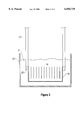
- FIG. 3 is a cross-sectional view of a robot end effector in the course of wet wafer processing.
- a wet wafer processing robot 10 may be utilized to automate the wet processing of semiconductor wafers and to facilitate the transfer of the wafers from station to station in a semiconductor process.
- a variety of robots are specially adapted to this operation, including the robots distributed by STEAG MicroTech, Inc., Austin, Tex.
- the wet wafer processing robot connects via bolts (not shown) and the plate 44 to an end effector 12 which is connected to end effector fingers 14.
- End effector fingers 14 are designed to engage a wafer carrier 16, as shown in FIG. 2.
- the carrier 16 holds a plurality of semiconductor wafers 18 on edge inside the carrier, as shown in FIG. 3. Because the carrier 16 is open, chemicals "A" inside the tank 20 are available to treat the wafers.
- the carrier 16 includes a handle frame 22 of a distinct shape.
- End effector fingers 14 include a hook-shaped portion 24 which is designed to engage the catch 40 of the carrier 16. The portion 24 enters the opening 42 in the frame 22, translates and is raised to engage the catch 40.
- the end effector fingers 14 are exposed to severe chemical environments used for wafer etching, cleaning or the like.
- the end effector fingers 14 are adapted to removably connect to the remainder of the robot end effector 12.
- the shank 26 of the end effector 12 includes a notch 29.
- a pair of pins 28 extend transversely to the length of the effector finger 14 to engage slots 30 on the face 32 of the arm 12. The pins 28 guide the effector finger 14 into alignment with the remainder of the end effector 12.
- a socket head cap screw 38 extends through the shank 26 and threads into a threaded aperture 34 in the robot end effector 14.
- the end effector finger 14 can be made of a corrosion resistant material such as stainless steel.
- the end effector finger 14 are coated with a corrosion resistant film such as fluorocarbon.
- the end effector fingers 14 may be readily removed from the rest of the robot arm to facilitate cleaning, treatment and maintenance. After use, the end effector finger 14 can be readily returned to its precise position on the robot end effector 12. It is important that the end effector finger be precisely positioned since the robot only knows programmed movements and cannot accommodate for changes in alignment of the end effector fingers 14.
Abstract
Description
Claims (8)
Priority Applications (1)
| Application Number | Priority Date | Filing Date | Title |
|---|---|---|---|
| US08/980,702 US6050739A (en) | 1997-12-01 | 1997-12-01 | Robot end effector for automated wet wafer processing |
Applications Claiming Priority (1)
| Application Number | Priority Date | Filing Date | Title |
|---|---|---|---|
| US08/980,702 US6050739A (en) | 1997-12-01 | 1997-12-01 | Robot end effector for automated wet wafer processing |
Publications (1)
| Publication Number | Publication Date |
|---|---|
| US6050739A true US6050739A (en) | 2000-04-18 |
Family
ID=25527782
Family Applications (1)
| Application Number | Title | Priority Date | Filing Date |
|---|---|---|---|
| US08/980,702 Expired - Fee Related US6050739A (en) | 1997-12-01 | 1997-12-01 | Robot end effector for automated wet wafer processing |
Country Status (1)
| Country | Link |
|---|---|
| US (1) | US6050739A (en) |
Cited By (5)
| Publication number | Priority date | Publication date | Assignee | Title |
|---|---|---|---|---|
| US20030051974A1 (en) * | 1997-05-05 | 2003-03-20 | Semitool, Inc. | Automated semiconductor processing system |
| US20050285419A1 (en) * | 2004-06-25 | 2005-12-29 | Takayuki Matsumoto | Multiple section end effector assembly |
| US8276959B2 (en) | 2008-08-08 | 2012-10-02 | Applied Materials, Inc. | Magnetic pad for end-effectors |
| US8322766B1 (en) | 2011-11-02 | 2012-12-04 | Gintech Energy Corporation | Wafer gripper |
| EP2590209A1 (en) * | 2011-11-01 | 2013-05-08 | Gintech Energy Corporation | Gripper |
Citations (10)
| Publication number | Priority date | Publication date | Assignee | Title |
|---|---|---|---|---|
| US3656393A (en) * | 1970-06-19 | 1972-04-18 | Paramount Textile Mach Co | Carbide saw blade locking device |
| US4461195A (en) * | 1982-03-26 | 1984-07-24 | Barnick John F | Multi-machine cutter holder |
| US4518349A (en) * | 1983-12-01 | 1985-05-21 | Better Semiconductor Processes (Bsp) | Cantilevered boat-free semiconductor wafer handling system |
| US4604027A (en) * | 1984-06-21 | 1986-08-05 | At&T Technologies, Inc. | Manipulator of articles and methods of moving articles over an extended distance |
| US5295777A (en) * | 1992-12-23 | 1994-03-22 | Materials Research Corporation | Wafer transport module with rotatable and horizontally extendable wafer holder |
| US5440971A (en) * | 1992-10-21 | 1995-08-15 | Yuda; Lawrence F. | Cylinder with mounting for guide rods |
| US5570994A (en) * | 1993-07-15 | 1996-11-05 | Applied Materials, Inc. | Wafer tray and ceramic blade for semiconductor processing apparatus |
| US5613793A (en) * | 1993-08-21 | 1997-03-25 | Dennis; Mark A. | Concealed fixing device |
| US5679160A (en) * | 1995-06-07 | 1997-10-21 | Nd Industries, Inc. | Apparatus for coating threaded fasteners |
| US5759268A (en) * | 1995-11-07 | 1998-06-02 | Sputtered Films, Inc. | System for providing a controlled deposition on wafers |
-
1997
- 1997-12-01 US US08/980,702 patent/US6050739A/en not_active Expired - Fee Related
Patent Citations (10)
| Publication number | Priority date | Publication date | Assignee | Title |
|---|---|---|---|---|
| US3656393A (en) * | 1970-06-19 | 1972-04-18 | Paramount Textile Mach Co | Carbide saw blade locking device |
| US4461195A (en) * | 1982-03-26 | 1984-07-24 | Barnick John F | Multi-machine cutter holder |
| US4518349A (en) * | 1983-12-01 | 1985-05-21 | Better Semiconductor Processes (Bsp) | Cantilevered boat-free semiconductor wafer handling system |
| US4604027A (en) * | 1984-06-21 | 1986-08-05 | At&T Technologies, Inc. | Manipulator of articles and methods of moving articles over an extended distance |
| US5440971A (en) * | 1992-10-21 | 1995-08-15 | Yuda; Lawrence F. | Cylinder with mounting for guide rods |
| US5295777A (en) * | 1992-12-23 | 1994-03-22 | Materials Research Corporation | Wafer transport module with rotatable and horizontally extendable wafer holder |
| US5570994A (en) * | 1993-07-15 | 1996-11-05 | Applied Materials, Inc. | Wafer tray and ceramic blade for semiconductor processing apparatus |
| US5613793A (en) * | 1993-08-21 | 1997-03-25 | Dennis; Mark A. | Concealed fixing device |
| US5679160A (en) * | 1995-06-07 | 1997-10-21 | Nd Industries, Inc. | Apparatus for coating threaded fasteners |
| US5759268A (en) * | 1995-11-07 | 1998-06-02 | Sputtered Films, Inc. | System for providing a controlled deposition on wafers |
Cited By (6)
| Publication number | Priority date | Publication date | Assignee | Title |
|---|---|---|---|---|
| US20030051974A1 (en) * | 1997-05-05 | 2003-03-20 | Semitool, Inc. | Automated semiconductor processing system |
| US20050285419A1 (en) * | 2004-06-25 | 2005-12-29 | Takayuki Matsumoto | Multiple section end effector assembly |
| US7073834B2 (en) * | 2004-06-25 | 2006-07-11 | Applied Materials, Inc. | Multiple section end effector assembly |
| US8276959B2 (en) | 2008-08-08 | 2012-10-02 | Applied Materials, Inc. | Magnetic pad for end-effectors |
| EP2590209A1 (en) * | 2011-11-01 | 2013-05-08 | Gintech Energy Corporation | Gripper |
| US8322766B1 (en) | 2011-11-02 | 2012-12-04 | Gintech Energy Corporation | Wafer gripper |
Similar Documents
| Publication | Publication Date | Title |
|---|---|---|
| TWI765001B (en) | Semiconductor manufacturing apparatus, failure prediction method for semiconductor manufacturing apparatus, and failure prediction program for semiconductor manufacturing apparatus | |
| US5692873A (en) | Apparatus for holding a piece of semiconductor | |
| CN1072389C (en) | Equipment for transferring semiconductor chip | |
| EP0778611A2 (en) | End effector for semiconductor wafer transfer device and method of moving a wafer with an end effector | |
| US20210146554A1 (en) | Multi-finger robot apparatus, electronic device manufacturing apparatus, and methods adapted to transport multiple substrates in electronic device manufacturing | |
| WO1999050891A1 (en) | A programmable substrate support for a substrate system | |
| US6050739A (en) | Robot end effector for automated wet wafer processing | |
| KR100704246B1 (en) | Substrate treatment system, substrate treatment device, program, and recording medium | |
| US6267423B1 (en) | End effector for semiconductor wafer transfer device and method of moving a wafer with an end effector | |
| US6451118B1 (en) | Cluster tool architecture for sulfur trioxide processing | |
| US20050110292A1 (en) | Ceramic end effector for micro circuit manufacturing | |
| SG181412A1 (en) | Edge grip end effector | |
| KR20080093878A (en) | Adjustable wrist design for robotic arm | |
| US6475567B2 (en) | Method of staining semiconductor wafer samples with a semiconductor treatment chemical | |
| KR101187844B1 (en) | Small lot size lithography bays | |
| US20040179932A1 (en) | Robotic hand with multi-wafer end effector | |
| US6625556B1 (en) | Wafer rotation randomization for process defect detection in semiconductor fabrication | |
| JPH07130637A (en) | Semiconductor manufacturing equipment | |
| JP6650073B2 (en) | Method and apparatus for processing a wafer-like substrate and use of the apparatus | |
| JPH07130638A (en) | Semiconductor manufacturing equipment | |
| US5149158A (en) | Wafer carrier holder for wafer carriers | |
| US6767407B2 (en) | Auto-centering device for mechanical clamp | |
| KR0134669Y1 (en) | Tweezer of handling for analysis inferiority of a semiconductor device | |
| KR100543441B1 (en) | A method and an apparatus for positioning of a semiconductor wafer transfer equipment | |
| US5100190A (en) | Wafer carrier holder for wafer carriers |
Legal Events
| Date | Code | Title | Description |
|---|---|---|---|
| FEPP | Fee payment procedure |
Free format text: PAYOR NUMBER ASSIGNED (ORIGINAL EVENT CODE: ASPN); ENTITY STATUS OF PATENT OWNER: LARGE ENTITY |
|
| AS | Assignment |
Owner name: MICRON TECHNOLOGY, INC., IDAHO Free format text: ASSIGNMENT OF ASSIGNORS INTEREST;ASSIGNOR:DUNN, L. BRIAN;REEL/FRAME:008875/0203 Effective date: 19971126 |
|
| FPAY | Fee payment |
Year of fee payment: 4 |
|
| FPAY | Fee payment |
Year of fee payment: 8 |
|
| REMI | Maintenance fee reminder mailed | ||
| LAPS | Lapse for failure to pay maintenance fees | ||
| STCH | Information on status: patent discontinuation |
Free format text: PATENT EXPIRED DUE TO NONPAYMENT OF MAINTENANCE FEES UNDER 37 CFR 1.362 |
|
| FP | Lapsed due to failure to pay maintenance fee |
Effective date: 20120418 |