US6053748A - PC card connection unit for micro SIM card - Google Patents
PC card connection unit for micro SIM card Download PDFInfo
- Publication number
- US6053748A US6053748A US08/837,421 US83742197A US6053748A US 6053748 A US6053748 A US 6053748A US 83742197 A US83742197 A US 83742197A US 6053748 A US6053748 A US 6053748A
- Authority
- US
- United States
- Prior art keywords
- card
- connector
- slot
- small
- circuit board
- Prior art date
- Legal status (The legal status is an assumption and is not a legal conclusion. Google has not performed a legal analysis and makes no representation as to the accuracy of the status listed.)
- Expired - Fee Related
Links
Images


Classifications
-
- H—ELECTRICITY
- H05—ELECTRIC TECHNIQUES NOT OTHERWISE PROVIDED FOR
- H05K—PRINTED CIRCUITS; CASINGS OR CONSTRUCTIONAL DETAILS OF ELECTRIC APPARATUS; MANUFACTURE OF ASSEMBLAGES OF ELECTRICAL COMPONENTS
- H05K5/00—Casings, cabinets or drawers for electric apparatus
- H05K5/02—Details
- H05K5/0256—Details of interchangeable modules or receptacles therefor, e.g. cartridge mechanisms
- H05K5/026—Details of interchangeable modules or receptacles therefor, e.g. cartridge mechanisms having standardized interfaces
- H05K5/0265—Details of interchangeable modules or receptacles therefor, e.g. cartridge mechanisms having standardized interfaces of PCMCIA type
- H05K5/0269—Card housings therefor, e.g. covers, frames, PCB
-
- G—PHYSICS
- G06—COMPUTING; CALCULATING OR COUNTING
- G06K—GRAPHICAL DATA READING; PRESENTATION OF DATA; RECORD CARRIERS; HANDLING RECORD CARRIERS
- G06K13/00—Conveying record carriers from one station to another, e.g. from stack to punching mechanism
- G06K13/02—Conveying record carriers from one station to another, e.g. from stack to punching mechanism the record carrier having longitudinal dimension comparable with transverse dimension, e.g. punched card
- G06K13/08—Feeding or discharging cards
- G06K13/0806—Feeding or discharging cards using an arrangement for ejection of an inserted card
-
- G—PHYSICS
- G06—COMPUTING; CALCULATING OR COUNTING
- G06K—GRAPHICAL DATA READING; PRESENTATION OF DATA; RECORD CARRIERS; HANDLING RECORD CARRIERS
- G06K7/00—Methods or arrangements for sensing record carriers, e.g. for reading patterns
- G06K7/0013—Methods or arrangements for sensing record carriers, e.g. for reading patterns by galvanic contacts, e.g. card connectors for ISO-7816 compliant smart cards or memory cards, e.g. SD card readers
- G06K7/0021—Methods or arrangements for sensing record carriers, e.g. for reading patterns by galvanic contacts, e.g. card connectors for ISO-7816 compliant smart cards or memory cards, e.g. SD card readers for reading/sensing record carriers having surface contacts
-
- H—ELECTRICITY
- H05—ELECTRIC TECHNIQUES NOT OTHERWISE PROVIDED FOR
- H05K—PRINTED CIRCUITS; CASINGS OR CONSTRUCTIONAL DETAILS OF ELECTRIC APPARATUS; MANUFACTURE OF ASSEMBLAGES OF ELECTRICAL COMPONENTS
- H05K5/00—Casings, cabinets or drawers for electric apparatus
- H05K5/02—Details
- H05K5/0256—Details of interchangeable modules or receptacles therefor, e.g. cartridge mechanisms
- H05K5/026—Details of interchangeable modules or receptacles therefor, e.g. cartridge mechanisms having standardized interfaces
- H05K5/0265—Details of interchangeable modules or receptacles therefor, e.g. cartridge mechanisms having standardized interfaces of PCMCIA type
- H05K5/0273—Details of interchangeable modules or receptacles therefor, e.g. cartridge mechanisms having standardized interfaces of PCMCIA type having extensions for peripherals, e.g. LAN, antennas
-
- H—ELECTRICITY
- H01—ELECTRIC ELEMENTS
- H01R—ELECTRICALLY-CONDUCTIVE CONNECTIONS; STRUCTURAL ASSOCIATIONS OF A PLURALITY OF MUTUALLY-INSULATED ELECTRICAL CONNECTING ELEMENTS; COUPLING DEVICES; CURRENT COLLECTORS
- H01R13/00—Details of coupling devices of the kinds covered by groups H01R12/70 or H01R24/00 - H01R33/00
- H01R13/02—Contact members
- H01R13/22—Contacts for co-operating by abutting
- H01R13/24—Contacts for co-operating by abutting resilient; resiliently-mounted
-
- H—ELECTRICITY
- H01—ELECTRIC ELEMENTS
- H01R—ELECTRICALLY-CONDUCTIVE CONNECTIONS; STRUCTURAL ASSOCIATIONS OF A PLURALITY OF MUTUALLY-INSULATED ELECTRICAL CONNECTING ELEMENTS; COUPLING DEVICES; CURRENT COLLECTORS
- H01R2107/00—Four or more poles
-
- H—ELECTRICITY
- H01—ELECTRIC ELEMENTS
- H01R—ELECTRICALLY-CONDUCTIVE CONNECTIONS; STRUCTURAL ASSOCIATIONS OF A PLURALITY OF MUTUALLY-INSULATED ELECTRICAL CONNECTING ELEMENTS; COUPLING DEVICES; CURRENT COLLECTORS
- H01R24/00—Two-part coupling devices, or either of their cooperating parts, characterised by their overall structure
- H01R24/60—Contacts spaced along planar side wall transverse to longitudinal axis of engagement
- H01R24/62—Sliding engagements with one side only, e.g. modular jack coupling devices
-
- Y—GENERAL TAGGING OF NEW TECHNOLOGICAL DEVELOPMENTS; GENERAL TAGGING OF CROSS-SECTIONAL TECHNOLOGIES SPANNING OVER SEVERAL SECTIONS OF THE IPC; TECHNICAL SUBJECTS COVERED BY FORMER USPC CROSS-REFERENCE ART COLLECTIONS [XRACs] AND DIGESTS
- Y10—TECHNICAL SUBJECTS COVERED BY FORMER USPC
- Y10S—TECHNICAL SUBJECTS COVERED BY FORMER USPC CROSS-REFERENCE ART COLLECTIONS [XRACs] AND DIGESTS
- Y10S439/00—Electrical connectors
- Y10S439/946—Memory card cartridge
Definitions
- the present invention relates to an electronic connection unit in the form of a PC card, for connecting to a small smart card such as a Micro Sim card.
- the invention more particularly relates to a PCMCIA (Personal Computer Memory Card International Association) standard PC card which can be inserted into a host such as a personal computer to make one or more connections between the small smart card and the computer and/or peripherals connected to a front end of the PC card.
- PCMCIA Personal Computer Memory Card International Association
- the PCMCIA standards relate to the external dimensions of the connection unit, in order to make it possible to insert a standard PC card into any personal computer which includes an insertion slot or passageway whose dimensions correspond to the PCMCIA standards.
- the present PC card or electronic connection unit in the general form of a card includes a metal shell made in two (possibly merging at one end) parts, with upper and lower parallel plane main walls and with side walls which, between them, form a cavity.
- a circuit board lies in the cavity and is spaced between the upper and lower walls.
- the circuit board may carry electronic components and, at its opposite longitudinal ends, PC card connectors and/or spacers.
- a connector at the PC card rear end can connect to a host connector lying at the rear of the host passageway. If the PC card has a PC card connector at its front end, such front connector may, for example, receive a plug for connection to a telephone line.
- Such small smart card comprises a plastic plate that is usually less than one millimeter thick, that usually has a memory that stores information, and has a group of contact pads for accessing the memory.
- This principle of authorizing access to a user owning a miniature or small smart card is commonly applied in the field of radiotelephony.
- a common smart card is a "MICRO SIM" card of standard dimensions.
- an electronic connection unit in the form of a PC card which allows a small smart card to be associated with it without considerably modifying the dimensional and structural (including EMI protection) characteristics of the PC card.
- a small smart card connector is mounted on the upper face of the circuit board that lies in the PC card.
- the shell of the PC card has a slot for passing the small smart card horizontally into the connector.
- the small smart card connector has an insulative connector housing with a pair of side guide edges and an inner stop for guiding a small smart card into a position where connector contacts engage contact pads on the small smart card;
- the small smart card connector housing has means for positioning it on the circuit board.
- the connector housing includes a plurality of spacers in the form of feet that extend through the circuit board and that have lower ends lying adjacent to or abutting the shell lower main wall. The upper end of the connector lies adjacent to or abuts the shell upper main wall.
- Means for extracting the card includes a notch which is formed in the upper main wall of the PC card.
- the notch can be elongated and extend parallel to the insertion direction. This allows a tool inserted through the notch to push the card or a carriage that holds the card, to slide the card outward.
- the notch can extend at least partly in line with the rear transverse edge of the fully inserted card, to allow the insertion of an extraction tool which engages the rear transverse edge of the card.
- a slidable carriage can be provided that includes an inner transverse edge that abuts the inner end of the small smart card.
- Means accessible from outside the PC card, is provided for controlling the sliding displacement of the carriage.
- the carriage is spring biased outwardly toward the extraction position, but is automatically retained in the insertion position by locking means.
- the means for automatically locking the carriage can include a retractable locking finger which is carried by the carriage. In the card insertion position, the finger is received in a hole in the upper main wall of the unit, the finger being upwardly biased into the hole.
- the means for automatically locking the carriage can include a retractable locking bar which is carried by the connector and which normally lies in a position for locking the card in the inserted position, with the bar being resiliently urged to that position.
- the locking bar normally blocks the card-receiving slot, but can be moved down by the inward end of a small smart card during insertion.
- Closure means are provided for at least partially closing the slot through which the small smart card is inserted.
- the closure means is resiliently deflectable and is automatically moved out of line with the slot when the card is inserted.
- the closure means is carried by the connector housing.
- the closure means include a closure lip which is mounted so as to move vertically with respect to the connector housing.
- the closure means includes a cam that interacts with the rear transverse edge of the card when the card is being inserted, in order to cause vertical movement of the lip.
- the lip is carried by two resiliently deflectable arms that extend along parallel sides of the connector housing. The closure lip is part of a closure seal.
- the upper main wall of the PC card can include a boss which, when the card is in the inserted position, faces a portion of the outer transverse edge of the card to prevent accidental ejection of this card from the unit.
- the bottom of the connector housing can include a ramp which causes the outer transverse edge of the card to be raised during movement for extracting it from the unit.
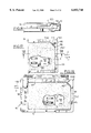
- FIG. 1 is an exploded perspective view of the main components of a PC card, or connection unit of the invention.
- FIG. 2A is a sectional view of a portion of the unit of FIG. 2, showing the boss thereof.
- FIG. 2 is a perspective view of a portion of the unit illustrated in FIG. 1, showing the slot for inserting the small card into the PC card.
- FIG. 3 is a plan view of a first embodiment of a smart card connector, intended to be installed in the connection unit of FIGS. 1 and 2.
- FIG. 4 is a side view taken along arrow F4 of FIG. 3, with the connector being shown upside-down.
- FIG. 5 is a side view taken along arrow F5 in FIG. 3.
- FIG. 6 is a partial cut-away plan view of the connection unit of FIG. 3, which shows the connector mounted on the circuit board, in proximity to the card insertion slot.
- FIG. 7 is a partially sectional view taken on line 7--7 in FIG. 6.
- FIG. 8 is a partial cut-away plan view of a connector of a second embodiment of the invention which, is equipped with a first type of card extraction carriage, wherein the carriage and the card are shown in the card insertion position and are also represented in phantom lines in the partial card extraction position.
- FIGS. 9 and 10 are views taken along arrows F9 and F10 respectively in FIG. 8, with the connector shown upside-down in FIG. 9.
- FIG. 11 is a plan view of a connector of a third embodiment of the invention, which is equipped with a second type of card extraction carriage, wherein the carriage and the card are shown in the card insertion position and are also represented in phantom lines in the partial card extraction position.
- FIG. 11A is a perspective view taken along arrow F11A in FIG. 11, which illustrates the design of the extraction carriage on a larger scale.
- FIG. 12 is a perspective view of a fourth embodiment of the connector which can be used in the PC card of FIGS. 1 and 2.
- FIG. 13 is a perspective view of the closure device intended to be mounted on the connector of FIG. 12.
- FIG. 14 is a cutaway partial plan view of the connector of the and closure device of FIGS. 12 and 13 shown assembled, with the card shown in the inserted position.
- FIG. 15 is a partial sectional view taken on line 15--15 of FIG. 14.
- FIG. 16 is a view similar to that of FIG. 15, but without the card.
- FIG. 17 is a partial cutaway plan view of another closure device, which also fulfills the function of a device for locking the card in the position in which it is inserted into the unit.
- FIG. 18 is a view taken on line 18--18 of FIG. 17.
- FIG. 19 is a partial cutaway plan view of an alternative embodiment of the locking and closure device illustrated in FIG. 18, in association with an alternative embodiment of the automatic extraction carriage illustrated in FIG. 11.
- FIG. 20 is a partial cutaway view of an alternative embodiment of the means for locking the card and the carriage in the card insertion position.
- FIG. 21 is a view taken on line F21 of FIG. 20, with the connector shown upside-down in FIG. 21.
- FIG. 22 is a sectional side view of another embodiment of a slot closure means, in the form of a flexible closure seal.
- FIG. 23 is a view similar to that of FIG. 22, which illustrates the closure seal when the card is in the full insertion position.
- FIG. 24 is a plan view of the connector of FIGS. 22 and 23, which illustrates the arrangement of the closure seal in the front part of the connector.
- FIG. 25 is a plan view of a connector of another embodiment of the invention.
- FIG. 26 is a view taken on line 26--26 of FIG. 25.
- FIG. 27 is a bottom view of the connector of FIG. 25.
- FIG. 28 is a plan view of a circuit board showing cut-outs therein for receiving the connector illustrated in FIGS. 25 to 27.
- FIG. 29 is a bottom view of the circuit board of FIG. 28, with the connector in place on the circuit board.
- FIG. 1 illustrates a connection unit 30 in the form of a PC card, of known general design, which includes a card housing 10 comprising a sheet metal shell.
- the shell includes upper and lower half-shells 32, 34, each of which is a piece of cut, stamped and folded sheet metal.
- the shapes and the dimensions of the shell are in accordance with the PCMCIA standard for PC cards, which specifies a length in directions R, F of 85.6 mm and a width in lateral direction L of 54 mm.
- the height in direction V is 5 mm.
- the card can be inserted into a standardized passageway 12 of a host 14 which, for example, may be a passage in a personal computer.
- the host has a host connector 16 at the rear end of the host passageway, with host contacts 17 that can mate with PC card contacts 19 at the rear of the PC card 30.
- the PC card 30 includes a circuit board 36 (which can hold circuit components) lying between the half-shells 32 and 34 and lying in a horizontal plane.
- the rear end of the PC card includes a rear connector 38 (shown in simplified form).
- the front end of the PC card is shown holding a front connector 40, though some cards have spacers thereat.
- the front connector 40 is designed to mate with a plug 42 which connects the PC card 30, for example, to a telecommunication line.
- the upper half-shell 32 has a horizontal planar upper main wall 44 which, in cooperation with a horizontal planar lower main wall 46 of the lower half-shell 34, forms a cavity 48 (FIG. 2) between them.
- the circuit board 36 extends in a horizontal plane parallel to the walls 44 and 46 and usually about halfway between the opposite facing faces 45 and 47 of the walls 44 and 46.
- the PC card 30 has laterally (L) opposite sides 50 and 52, which extend parallel to front and rear F, R longitudinal directions in the PC card of FIG. 1.
- the lower half shell 34 has vertically-extending sidewalls 54 and 56, which are crimped around the opposite side walls of the upper half-shell.
- One of the upper sidewalls is illustrated at 58 in FIG. 1.
- the frame 10 may be produced with a one-piece shell.
- the sides 50 and 52 of the connection unit or PC card 30 are in the form of rails for guiding the PC card in movement into the host passageway.
- the side end portions of the upper and lower half-shells 32, 34 have transition regions 60, 62 to give the sides 50 and 52 a height (e.g. 3.3 mm) which is less than the height (5 mm) at the middle of the PC card, where it is thickest.
- Each transition region such as the upper one 60 includes an inclined surface 82 which extends at an angle of more than 15° and up to 90° (or even slightly more) from the horizontal, and a primarily horizontal surface 84.
- a connector 64 is provided that is intended to receive a small smart card C with integrated circuit(s) of the "MICRO SIM” type, the connector lying within the PC card 30.
- the "MICRO SIM” card C may be referred to as a small smart card because it has a surface with contact pads (in zone 74 of its lower face 72) that provide electrical access to circuitry (usually primarily a memory chip) embedded in the rest of the smart card.
- the small card has a length, width, and thickness that are much less (less than 98% and usually less than 50%) of corresponding dimensions of the PCMCIA type 11 card.
- a "MICRO SIM” card has a length, width and thickness much less than 50% of the corresponding standard PC card dimensions (54 mm ⁇ 85.6 mm, with a thickness of 3.3 mm, 5 mm, and 10.5 mm, respectively, for type I, II, and III cards).
- the connector 64 includes a connector housing 66 of insulating material, with an upper face 68.
- the support forms a card-receiving recess 70 whose shape is complementary with that of the card C, and which can receive at least part of the card.
- the contact pads at 74 engage contacting ends 76 of contacts 78 of the connector.
- a plurality of the contact pads 74 may be connected, through contacts 78, to PC card contacts 19 at the rear of the PC card.
- the connector 66 of FIG. 1 is intended to be mounted with the lower face 67 of the connector housing 66 lying against the upper face 37 of the circuit board 36.
- the PC card housing frame 10 is formed with a slot 80 to allow insertion or extraction of the card C into or from the connector.
- the slot 80 is preferably located in or near one of the sides 50 of the PC card. As shown in FIG. 2., the insertion slot 80 is formed primarily in the inclined surface or part 82 of the side or transition region 60 of the upper half-shell 32. As discussed above, the transition region joins the upper main wall 44 to the horizontal surface part 84 where the PC card has a reduced-thickness side portion.
- the area 84' of the horizontal part 84 which extends in line with the bottom of the slot 80 in the inclined portion 82, is slightly angled downwardly and inwardly, at an angle of about 10°, with respect to the horizontal plane of the plane portion 84.
- the insertion slot 80 has vertically spaced upper and lower main edges 86, and 88 and has two end edges 90, 91.
- a horizontal slot axis 81 passes laterally through the middle of the slot.
- the slot does not extend into the main upper wall 44.
- the slot width measured in the general longitudinal direction (R, F) of the PC card, is slightly greater than the width of the card C, so as to allow insertion and extraction of the latter in inward and outward directions I, O, which are transverse to the general longitudinal direction (R, F) of the PC card.
- the recess 70 of the connector 64 has opposite edges 92 and 94 which extend parallel to the insertion direction I, and has an inner or inward edge 96 that extends perpendicular to the insertion direction.
- the inner edge 96 constitutes a stop for the rear transverse edge 98 (FIG. 6) of the card C.
- the card has opposite card edges 95 (FIG. 6) that are engaged by the recess edges.
- the connector housing 66 is open so as to allow insertion and extraction of the card C into and from the connector housing 66 by sliding it in the directions I, O parallel to the general horizontal plane of the card C.
- the height of the recess 70 is slightly greater than the thickness of the card C.
- the connector 64 has four feet 101 projecting downwardly D from the board-engaged face 67 of the connector housing 66.
- the feet 101 are in the form of cylindrical studs.
- the feet 101 position and fix the connector 64 on the circuit board 36.
- the circuit board has holes 100 (FIG. 1) through which the feet extend and which closely surround the holes to prevent horizontal movement of the connector.
- the feet 101 also serve a spacer function between the upper and lower main frame walls 46, 48 of the PC card 30, to prevent accidental crushing of the PC card.
- the height of the feet 101 is such that the lower end face 102 of each foot is in contact with the upper face 47 of the lower main wall 46, while the planar upper face 68 of the connector insulating support or connector housing 66 bears against the opposite lower face 45 of the upper main wall 44.
- the height of the card middle portion is 5 mm.
- the sheet metal upper and lower main walls 44, 46 each have a thickness of about 0.2 mm, so the distance H between the shell main walls is about 4.6 mm, or between 4 and 5 mm for type II PCMCIA card.
- the height H equals the height between the upper and lower horizontal main walls.
- the connector 64 has a recess or cutout 11 0 in its outer edge 1 12.
- the outer edge 112 is positioned on the circuit board 36, so the contact connection ends 77 (FIG. 5) which are soldered to circuit board traces, lie below an inward extension of the slot 80 in the PC card shell. This avoids an accidental short-circuit of the connection ends 77 of the contacts 78 by contact pads of the card.
- the outer edge 99 of the card is located entirely within the PC card 30.
- the outer edge 99 is slightly set-back from the upper slot edge 86 (FIG. 7) of the insertion slot 80.
- an additional cut-out may be provided in the edge of the slot 80.
- the PC card 30 thus has an outside "silhouette", after insertion of the card C, which is identical to that of a standard PC card, so as to allow it to be inserted into a corresponding slot of a personal computer.
- the insertion slot 80 has small dimensions, with a height of about 0.8 mm and a longitudinal (R, F) length of about 15 mm and a lateral (L) length of about 25 mm.
- the small slot does not greatly affect the rigidity of the PC card or the EMI (electromagnetic interference) blocking function of the shell.
- a notch or extraction groove 114 (FIG. 1) is provided in the upper main wall 44 of the shell.
- the notch 114 is shown by a phantom line in FIG. 6.
- the notch extends laterally (L) with respect to the PC card 30, i.e. parallel to the insertion and or extraction directions.
- the notch 114 extends both inward (I) and outward (0) of the rear or inner transverse edge 98 of the card C and, preferably, opposite a region of the connector 64 which does not include parts of the contacts 78.
- the notch extends to an outward portion 116 of the card housing recess so a tool can abut the inner edge of the fully inserted card.
- the notch 114 provides a passage for the insertion of a small tool (e.g. a toothpick) to push on the inner edge 98 of the card C to push it out from the connector housing recess 70.
- a small tool e.g. a toothpick
- the notch is long enough to cause the outer edge 99 of the small smart card to project considerably from the PC card through the slot 80.
- the projection (of a plurality of millimeters) is sufficient to allow the user to grasp the card to extract it fully from the PC card.
- the card C has a cut-out flat 116 at an outside of its outer edge 99.
- the cutout constitutes an orienting means for positioning the card C in a connector.
- the upper main wall 44 of the PC card shell may be formed with a depression, or boss 120 (FIGS. 1,2 and 2A).
- boss 120 projects slightly into the card-holding recess 70 to form a stop which lies outward of the card flat cutout 116.
- a slightly greater outward force must be applied to the inner end of the card to extract it.
- the slightly greater effort is required to resiliently deflect the upper main wall 44 of the PC card upwardly.
- the boss 120 rises as the cut-out flat 116 and then the upper face 73 of the card passes by.
- FIGS. 8 to 10 show a connector 64A whose connector housing includes a stationary body 69 and a carriage 130 for manual extraction of the small smart card C.
- the insulative body includes, on one of its side edges 132, a slideway 134 on which a carriage side portion 136 is slidably mounted.
- An extraction tab 138 of the carriage has an outer edge 142 for abutting the card, and has an inner edge 140 that abuts an inner transverse edge of the housing body 69 in the full insertion position of the card.
- the side 136 of the extraction carriage 130 includes a hollow 144 intended to receive the narrow end of a tool (e.g. a toothpick). Such tool is inserted into a notch 114A in the upper face 44 of the PC card.
- the notch 114A is similar to the notch 114 of FIG. 6, except that notch 114A extends from the location of hollow 144 and outwardly therefrom by several millimeters. This design is advantageous because the extraction tool T does not have to push directly against the inward edge 98 of the card C, thus preventing damage to the card.
- the slide upper face, in the form of a plate 137 of the sheet metal slide 130 extends around (and immediately below) the notch 114, in the upper main wall of the PC card, thus ensuring electromagnetic closure of the notch 114.
- FIGS. 11 and 11A The embodiment illustrated in FIGS. 11 and 11A will now be described, in which the connector 64B is equipped with a card extraction carriage 130B that has a stop surface 96B and that automatically extracts the card.
- the extraction carriage 130B is similar to the one in FIGS. 8 to 10, but is equipped with a tension coil spring 150 which urges the carriage outward.
- a first or inner end 152 of the spring is hooked on a lug 154 of the slide 130, while its opposite outer end 156 is hooked on a lug 158 formed on the stationary portion 69B of the connector.
- the spring 150 continuously urges the card C to retract from the PC card. In order to hold the card in the inserted position, illustrated in phantom lines in FIG.
- a means is provided for locking the extraction carriage 130 in the card insertion, or inward position.
- the locking means is formed by locking finger 160 which, in the card insertion position of the carriage, is received in a complementary hole 162 in the upper main wall 44 of the PC card.
- the finger 160 can be formed by a boss or a ball fixed to the end of an arm 166 which extends from the extraction carriage 130 or can be a bent end of the arm.
- the bar or arm 166 can be bent down by its resilient deflection (or by a pivot joint and spring) to release the locking finger 160 from the hole 162, using a person's fingernail or a tool to depress the finger.
- the carriage and card then automatically slide outward, with the finger 160 rubbing against the lower face 45 of the upper main wall 44 of the PC card.
- the automatic extraction carriage 130B that is moved outward by the extraction spring 150, makes it possible to do without the notch 114 in the unit 30, and to replace it by a simple small hole 162.
- the hole 162 is closed either by the locking finger 160, or by a portion of the upper face 167 of the arm 166, during outward extraction travel of the carriage 130B.
- FIGS. 12 to 16 show an insulative connector housing 66D that is modified to include a slot closure device.
- FIG. 12 shows a connector housing 66D with edge guides 92, 94 defining a horizontal guide plane 95 between them.
- the connector housing forms two longitudinally opposite ribs 170 for supporting the closure device 172 of FIG. 13.
- the closure device 172 which is preferably formed of sheet metal includes a closure lip 174 of a generally hollow semi cylindrical shape.
- the lip has a convex upper face 176 that faces primarily upwards and that lies inward of and in line with the slot 80 (i.e. in line with a horizontal axis 81 of the slot).
- the closure lip 174 is mounted on the outer ends of two parallel arms 178. Each arm carries a U-shaped tab 180 at its inner end for attaching the closure device to the connector 164 by inserting the ribs 170 into the attachment tabs.
- the arms 178 which carry the closure lip 174 extend outwardly from the bottom of the ribs 170. By being flexed vertically, the arms allow primarily vertical displacement of the lip 174.
- the lip 174 lies inward of the slot 80 in the PC card. It is noted that in FIG. 16 the slot 80 extends slightly into the PC card by projecting slightly into the upper main wall 44.
- the closure lip 174 retracts by moving down automatically when the card C is inserted in the direction I. This is because during card insertion the rear transverse edge 98 of the card C presses against the closure upper face 176 which acts as a cam to cause bending of the arms 178 and downward movement of the closure lip. While the card is slid inwardly, the lip 174 presses up against the lower face 72 of the card.
- the closure device 172D also constitutes a device for retaining the card C in its fully inserted position.
- the arms 178D are slightly longer and the lip 174D includes a rear barrier 180 with a part at 182 which is complementary to the cutout flat 116 at the outer edge 99 of the card.
- FIG. 13 shows the shape of the barrier at 181 in phantom lines.
- the closure device 172E is similar to the one illustrated in FIGS. 17 and 18, but is associated with an extraction carriage 130 of the type described in FIGS. 11 and 11A, with a spring 150.
- a lug 158 for attaching the extraction spring 150 can be formed integrally with the closure device 172E. This enables simplification of the extraction carriage 130 because it does not require its own means for locking the card in the inserted position, locking being ensured by the closure device 172E.
- the card is continuously urged outwardly by the extraction carriage 130E so the card outer edge 99 abuts against the edge of the outer barrier 180 of the lip 174D. To cause automatic extraction of the card C, it is sufficient to downwardly deflect the lip 174 through the slot 80. Once the lip barrier 180 (also indicated in FIG. 13) moves below the outer edge of the card, the card is automatically moved outward by the extraction carriage 130.
- the device for locking the card consists of a rocker bar 200 which is mounted so as to pivot on the housing of the connector 64F about a pin 202.
- the extraction spring 150 is hooked on a lug 158F which is carried by the rocker bar 200 so as to urge the latter continuously into the card locking position.
- the outer barrier 180F of the rocker bar 200 lie outward of the outer edge 99 of the card when the latter is in the inserted position, as is illustrated in FIG. 20. If the outer end of the rocker bar is depressed, the carriage pushes out the card.
- the connector is shown "upside-down" in FIG. 21, in that the feet 101,102 for mounting on a circuit board project upwardly.
- the upper face 174F of the rocker bar 200 fulfills a function equivalent to that of the closure lip 174, insofar as it can extend in line with the slot 80 to seal the slot and prevent card extraction.
- FIGS. 22 to 24 illustrate another design of the means for closing the slot 80, comprising of a closure seal 220.
- the closure seal lies in a connector housing portion 222 formed in the connector housing 66G of the connector 64G near the outer edge of the connector.
- the closure seal 220 has a sealing lip 174G which normally lies closely inward of the insertion slot 80, that is when there is no small smart card in the PC card 30.
- the closure seal is retracted by resilient deformation when a card C is inserted into the PC card 30 through the slot 80, as is illustrated in FIG. 23.
- the closure seal 220 has a base 224 mounted on the connector housing part 222.
- a ramp 226 is provided in the connector housing 64G to facilitate insertion of the card, that is, to bring it level with the bottom of the connector housing.
- FIGS. 25 to 27 illustrate another connector housing which is intended to be mounted in association with a printed-circuit board 36H that is illustrated partially in FIGS. 28 and 29.
- the connector 64H has an upper part intended to extend below the upper face 37 of the circuit board 36H, the thickness of which is preferably less than in the earlier embodiments described above.
- a part of the connector housing has a lower face 67 which bears on the upper face 37 of the circuit board 36, and has a lower housing part that extends below the connector housing lower face 67.
- the lower part comprises three blocks 230, 232 and 234, of rectangular contour, each of which is intended to extend into a complementarily shaped opening 230', 232', 234', respectively, formed in the circuit board 36H.
- the end blocks 230 and 234 fix the positions of the contacts, while the central block 232 allows the deflectable contact parts to move down.
- parts of the connector 64H other than its feet may project from one or both faces of the circuit board 36.
- the connector 64 is positioned, with respect to the circuit board 36, by the blocks 230, 232 and 234.
- one or more of the blocks may include feet forming spacers.
- the bottom of the connector housing includes a ramp 236 which makes it possible to raise the card when it is being extracted.
- the ramp 236 directs the card through the slot 80 and in a path to clear a thin step which is constituted by a stop for retaining the card in the connector and which is adjacent to the ramp.
- the boss 120 in FIG. 2 is superfluous.
- the slot 80 may be arranged with the insertion/extraction directions I, O parallel to the general longitudinal direction (R, F) of the PC card, and a slot for passing a small smart card may lie at the front end of the PC card in a spacer thereat.
Abstract
Description
Claims (24)
Applications Claiming Priority (2)
| Application Number | Priority Date | Filing Date | Title |
|---|---|---|---|
| FR9604842A FR2747847B1 (en) | 1996-04-18 | 1996-04-18 | ELECTRONIC CONNECTION BOX, TO A PERSONAL COMPUTER, EQUIPPED WITH A CONNECTOR FOR A CHIP CARD |
| FR9604842 | 1996-04-18 |
Publications (1)
| Publication Number | Publication Date |
|---|---|
| US6053748A true US6053748A (en) | 2000-04-25 |
Family
ID=9491324
Family Applications (1)
| Application Number | Title | Priority Date | Filing Date |
|---|---|---|---|
| US08/837,421 Expired - Fee Related US6053748A (en) | 1996-04-18 | 1997-04-17 | PC card connection unit for micro SIM card |
Country Status (10)
| Country | Link |
|---|---|
| US (1) | US6053748A (en) |
| EP (4) | EP0942492B1 (en) |
| JP (4) | JP3313732B2 (en) |
| CN (3) | CN1157680C (en) |
| CA (1) | CA2221890C (en) |
| DE (4) | DE69706958T2 (en) |
| FR (1) | FR2747847B1 (en) |
| HK (1) | HK1027677A1 (en) |
| TW (4) | TW420787B (en) |
| WO (1) | WO1997039418A1 (en) |
Cited By (24)
| Publication number | Priority date | Publication date | Assignee | Title |
|---|---|---|---|---|
| WO2000068770A1 (en) * | 1999-05-11 | 2000-11-16 | Socket Communications, Inc. | High-density removable expansion module having i/o and second-level removable expansion memory |
| US6325637B1 (en) * | 1999-07-19 | 2001-12-04 | Nokia Mobile Phone Limited | Card reader |
| DE10038287A1 (en) * | 2000-08-05 | 2002-02-21 | Itt Mfg Enterprises Inc | Plug-in card for electronic devices |
| US6353870B1 (en) * | 1999-05-11 | 2002-03-05 | Socket Communications Inc. | Closed case removable expansion card having interconnect and adapter circuitry for both I/O and removable memory |
| US6561851B2 (en) | 2001-04-27 | 2003-05-13 | Sierra Wireless Inc. | Module interface for PC card |
| WO2003055009A1 (en) * | 2001-12-11 | 2003-07-03 | Molex Incorporated | Secure digital memory card socket |
| US6641441B2 (en) * | 2001-12-26 | 2003-11-04 | Hon Hai Precision Ind. Co., Ltd. | Electronic card connector having improved assembly |
| US6781831B1 (en) | 2002-02-14 | 2004-08-24 | Mercury Computer Systems, Inc. | Card-cage with integrated control and shaping of flow resistance curve for multiple plenum chambers |
| US6808396B2 (en) * | 2002-05-24 | 2004-10-26 | Symbol Technologies, Inc. | Connection of a user identity module to a compact card case |
| US20050033848A1 (en) * | 2002-04-08 | 2005-02-10 | Martin Croome | Wireless enabled memory module |
| US6879486B1 (en) | 2002-02-14 | 2005-04-12 | Mercury Computer Systems, Inc. | Central inlet circuit board assembly |
| US6951470B1 (en) * | 2004-10-22 | 2005-10-04 | Huang-Chou Huang | SIM card seat assembly |
| US20050223129A1 (en) * | 2004-04-02 | 2005-10-06 | Arm Limited | Arbitration of data transfer requests |
| US20060121941A1 (en) * | 2004-12-03 | 2006-06-08 | Shiflett Jamie C | SIM card retaining device |
| US20060124739A1 (en) * | 2002-10-25 | 2006-06-15 | Yutaka Kojima | Memory card adapter for connecting a miniature card to a standard card connector, along with a method of fabricating same |
| DE102006021023A1 (en) * | 2006-04-28 | 2007-10-31 | Würth Elektronik Rot am See GmbH & Co. KG | modules structure |
| US20080124964A1 (en) * | 2006-11-27 | 2008-05-29 | K.S. Terminals, Inc. | Card connection apparatus and its applications |
| US20090172235A1 (en) * | 2007-12-27 | 2009-07-02 | Mei Yan | Megasim card adapter |
| US20100184310A1 (en) * | 2009-01-15 | 2010-07-22 | J.S.T. Mfg. Co., Ltd. | IC card |
| US8371866B1 (en) * | 2011-09-09 | 2013-02-12 | Cheng Uei Precision Industry Co., Ltd. | Card connector |
| US20130058052A1 (en) * | 2009-01-13 | 2013-03-07 | Dy 4 Systems Inc. | Tamper Respondent Module |
| US20140038533A1 (en) * | 2012-03-31 | 2014-02-06 | Xianming Zhuang | Intelligent terminal that allows for replacement of a wireless communication device by a user |
| US8651884B1 (en) | 2012-04-10 | 2014-02-18 | Google Inc. | Ejectable memory card tray in a universal serial bus (USB) connector |
| US20180316377A1 (en) * | 2015-12-31 | 2018-11-01 | Molex, Llc | Card socket, card connector, and manufacturing method therefor |
Families Citing this family (12)
| Publication number | Priority date | Publication date | Assignee | Title |
|---|---|---|---|---|
| DE29722142U1 (en) * | 1997-12-16 | 1998-02-12 | Stocko Metallwarenfab Henkels | Adapter for contacting chip cards |
| FR2773275B1 (en) * | 1997-12-26 | 2000-01-28 | Itt Mfg Enterprises Inc | VERY LOW THICKNESS ELECTRICAL CONNECTOR FOR CONNECTION OF AN ELECTRONIC MEMORY CARD |
| DE19815549C2 (en) * | 1998-04-07 | 2000-04-27 | Itt Mfg Enterprises Inc | Plug-in card for electronic devices |
| DE19846366C2 (en) * | 1998-04-07 | 2000-07-27 | Itt Mfg Enterprises Inc | Plug-in card for electronic devices |
| DE29904904U1 (en) * | 1999-03-17 | 1999-06-10 | Scm Microsystems Gmbh | Chip card reader with contacting unit |
| DE19925146C2 (en) * | 1999-06-02 | 2003-01-09 | Itt Mfg Enterprises Inc | Plug-in card for electronic devices |
| JP2001125662A (en) | 1999-08-18 | 2001-05-11 | Fujitsu Ltd | Extension device with authentication information input means for information processor, authentication information input unit, and information processor |
| DE19940695B4 (en) * | 1999-08-27 | 2008-03-27 | ITT Manufacturing Enterprises, Inc., Wilmington | Electronic media device |
| DE19947162C1 (en) * | 1999-10-01 | 2000-09-28 | Itt Mfg Enterprises Inc | Plug-in card for electronic equipment has frame element attached to housing part; chip card can be inserted into frame element to contacting device at end of frame element |
| CN101452537B (en) * | 2007-11-30 | 2011-11-16 | 深圳富泰宏精密工业有限公司 | Chip card fixing device and portable electronic device with the fixing device |
| US9604671B2 (en) | 2015-08-13 | 2017-03-28 | Fca Us Llc | Vehicle underbody structure |
| FR3115905B1 (en) * | 2020-10-30 | 2023-03-03 | Banks And Acquirers Int Holding | Solderable chip card connector and corresponding mounting method. |
Citations (8)
| Publication number | Priority date | Publication date | Assignee | Title |
|---|---|---|---|---|
| EP0480334A1 (en) * | 1990-10-08 | 1992-04-15 | Alcatel Cit | Device mainly functionning as a chip card reader |
| FR2670926A1 (en) * | 1990-11-26 | 1992-06-26 | Motorola Inc | CHIP CARD READER, ESPECIALLY OF THE SUBSCRIBER IDENTIFICATION MODULE TYPE FOR RADIOTELEPHONE. |
| EP0595025A2 (en) * | 1992-10-30 | 1994-05-04 | The Whitaker Corporation | An assembly of an electrical connector and ejector unit for connecting IC cards to printed circuit boards |
| DE29505678U1 (en) * | 1995-04-01 | 1995-06-14 | Stocko Metallwarenfab Henkels | Contact unit for card-shaped carrier elements |
| US5505628A (en) * | 1993-06-07 | 1996-04-09 | Methode Electronics, Inc. | Memory card frame and cover kit |
| DE29602632U1 (en) * | 1996-02-05 | 1996-05-30 | Neifer Wolfgang | Mobile chip card reading module |
| US5563400A (en) * | 1993-10-06 | 1996-10-08 | Gemplus Card International | Multi-applications portable card for personal computer |
| US5752857A (en) * | 1996-05-24 | 1998-05-19 | Itt Corporation | Smart card computer adaptor |
Family Cites Families (3)
| Publication number | Priority date | Publication date | Assignee | Title |
|---|---|---|---|---|
| DE2326543C3 (en) * | 1973-05-24 | 1979-08-30 | Siemens Ag, 1000 Berlin Und 8000 Muenchen | Holder for a cable plug |
| FR2607291B1 (en) * | 1986-11-21 | 1991-04-19 | Flonic Sa | CONNECTION ASSEMBLY FOR ELECTRONIC MEMORY CARDS AND READ / WRITE DEVICE USING THE SAME |
| JPH0492380A (en) * | 1990-08-06 | 1992-03-25 | Fuji Electric Co Ltd | Female connector |
-
1996
- 1996-04-18 FR FR9604842A patent/FR2747847B1/en not_active Expired - Fee Related
-
1997
- 1997-04-07 DE DE69706958T patent/DE69706958T2/en not_active Expired - Fee Related
- 1997-04-07 JP JP53691197A patent/JP3313732B2/en not_active Expired - Fee Related
- 1997-04-07 CN CNB971903883A patent/CN1157680C/en not_active Expired - Fee Related
- 1997-04-07 EP EP99201075A patent/EP0942492B1/en not_active Expired - Lifetime
- 1997-04-07 EP EP97923269A patent/EP0846304B1/en not_active Expired - Lifetime
- 1997-04-07 CA CA002221890A patent/CA2221890C/en not_active Expired - Fee Related
- 1997-04-07 DE DE69723461T patent/DE69723461T2/en not_active Expired - Fee Related
- 1997-04-07 DE DE69713871T patent/DE69713871T2/en not_active Expired - Fee Related
- 1997-04-07 DE DE69713564T patent/DE69713564T2/en not_active Expired - Fee Related
- 1997-04-07 WO PCT/IB1997/000595 patent/WO1997039418A1/en active IP Right Grant
- 1997-04-07 EP EP98201407A patent/EP0860905B1/en not_active Expired - Lifetime
- 1997-04-07 EP EP98201406A patent/EP0860904B1/en not_active Expired - Lifetime
- 1997-04-15 TW TW088106284A patent/TW420787B/en not_active IP Right Cessation
- 1997-04-15 TW TW087106992A patent/TW420786B/en not_active IP Right Cessation
- 1997-04-15 TW TW086104823A patent/TW416039B/en not_active IP Right Cessation
- 1997-04-15 TW TW087106991A patent/TW420785B/en not_active IP Right Cessation
- 1997-04-17 US US08/837,421 patent/US6053748A/en not_active Expired - Fee Related
-
1998
- 1998-05-22 CN CN98108935A patent/CN1117417C/en not_active Expired - Fee Related
- 1998-06-18 JP JP17141798A patent/JP3974259B2/en not_active Expired - Fee Related
- 1998-06-18 JP JP17141898A patent/JP3974260B2/en not_active Expired - Fee Related
-
1999
- 1999-04-27 JP JP11920899A patent/JP3902350B2/en not_active Expired - Fee Related
- 1999-09-27 CN CN99120718.1A patent/CN1118908C/en not_active Expired - Fee Related
-
2000
- 2000-10-18 HK HK00106594A patent/HK1027677A1/en not_active IP Right Cessation
Patent Citations (8)
| Publication number | Priority date | Publication date | Assignee | Title |
|---|---|---|---|---|
| EP0480334A1 (en) * | 1990-10-08 | 1992-04-15 | Alcatel Cit | Device mainly functionning as a chip card reader |
| FR2670926A1 (en) * | 1990-11-26 | 1992-06-26 | Motorola Inc | CHIP CARD READER, ESPECIALLY OF THE SUBSCRIBER IDENTIFICATION MODULE TYPE FOR RADIOTELEPHONE. |
| EP0595025A2 (en) * | 1992-10-30 | 1994-05-04 | The Whitaker Corporation | An assembly of an electrical connector and ejector unit for connecting IC cards to printed circuit boards |
| US5505628A (en) * | 1993-06-07 | 1996-04-09 | Methode Electronics, Inc. | Memory card frame and cover kit |
| US5563400A (en) * | 1993-10-06 | 1996-10-08 | Gemplus Card International | Multi-applications portable card for personal computer |
| DE29505678U1 (en) * | 1995-04-01 | 1995-06-14 | Stocko Metallwarenfab Henkels | Contact unit for card-shaped carrier elements |
| DE29602632U1 (en) * | 1996-02-05 | 1996-05-30 | Neifer Wolfgang | Mobile chip card reading module |
| US5752857A (en) * | 1996-05-24 | 1998-05-19 | Itt Corporation | Smart card computer adaptor |
Cited By (51)
| Publication number | Priority date | Publication date | Assignee | Title |
|---|---|---|---|---|
| US6976111B1 (en) | 1999-05-11 | 2005-12-13 | Socket Communications, Inc. | High-density removable expansion module having I/O and second-level removable expansion memory |
| US20040039860A1 (en) * | 1999-05-11 | 2004-02-26 | Socket Communications, Inc. | Nested removable-removable modules with game and media-player applications |
| GB2365182A (en) * | 1999-05-11 | 2002-02-13 | Socket Communications Inc | High-density removable expansion module having I/O and second-level removable expansion memory |
| US20050235086A1 (en) * | 1999-05-11 | 2005-10-20 | Mills Kevin J | Portable GPS methods and devices |
| US6353870B1 (en) * | 1999-05-11 | 2002-03-05 | Socket Communications Inc. | Closed case removable expansion card having interconnect and adapter circuitry for both I/O and removable memory |
| US20060164891A1 (en) * | 1999-05-11 | 2006-07-27 | Socket Communications, Inc. | Removable modules with external I/O flexibility via an integral second-level removable slot |
| US20090287870A1 (en) * | 1999-05-11 | 2009-11-19 | Mills Kevin J | Removable wireless expansion card having a removable subscriber information module |
| US6599147B1 (en) | 1999-05-11 | 2003-07-29 | Socket Communications, Inc. | High-density removable expansion module having I/O and second-level-removable expansion memory |
| US6920517B2 (en) | 1999-05-11 | 2005-07-19 | Socket Communications, Inc. | Nested removable-removable modules with game and media-player applications |
| US6691196B2 (en) | 1999-05-11 | 2004-02-10 | Socket Communications, Inc. | First-level removable module having bar code I/O and second-level removable memory |
| GB2365182B (en) * | 1999-05-11 | 2004-02-11 | Socket Communications Inc | High-density removable expansion module having I/O and second-level removable expansion memory |
| US6863557B2 (en) | 1999-05-11 | 2005-03-08 | Socket Communications, Inc. | High-density removable expansion module having I/O and second-level-removable expansion memory |
| US20040048503A1 (en) * | 1999-05-11 | 2004-03-11 | Mills Kevin J. | High-density removable expansion module having I/O and second-level-removable expansion memory |
| US7194565B2 (en) * | 1999-05-11 | 2007-03-20 | Socket Communications, Inc. | Nested removable-removable expansion modules |
| US7454541B2 (en) | 1999-05-11 | 2008-11-18 | Socket Mobile, Inc. | Removable wireless expansion card having a removable subscriber information module |
| US20040257756A1 (en) * | 1999-05-11 | 2004-12-23 | Mills Kevin J. | Removable wireless expansion card having a removable subscriber information module |
| US20040268001A1 (en) * | 1999-05-11 | 2004-12-30 | Mills Kevin J | Nested removable-removable expansion modules |
| US7343439B2 (en) * | 1999-05-11 | 2008-03-11 | Socket Communications, Inc. | Removable modules with external I/O flexibility via an integral second-level removable slot |
| WO2000068770A1 (en) * | 1999-05-11 | 2000-11-16 | Socket Communications, Inc. | High-density removable expansion module having i/o and second-level removable expansion memory |
| US6325637B1 (en) * | 1999-07-19 | 2001-12-04 | Nokia Mobile Phone Limited | Card reader |
| DE10038287A1 (en) * | 2000-08-05 | 2002-02-21 | Itt Mfg Enterprises Inc | Plug-in card for electronic devices |
| US6561851B2 (en) | 2001-04-27 | 2003-05-13 | Sierra Wireless Inc. | Module interface for PC card |
| WO2003055009A1 (en) * | 2001-12-11 | 2003-07-03 | Molex Incorporated | Secure digital memory card socket |
| US6641441B2 (en) * | 2001-12-26 | 2003-11-04 | Hon Hai Precision Ind. Co., Ltd. | Electronic card connector having improved assembly |
| US6781831B1 (en) | 2002-02-14 | 2004-08-24 | Mercury Computer Systems, Inc. | Card-cage with integrated control and shaping of flow resistance curve for multiple plenum chambers |
| US6879486B1 (en) | 2002-02-14 | 2005-04-12 | Mercury Computer Systems, Inc. | Central inlet circuit board assembly |
| US7440774B2 (en) | 2002-04-08 | 2008-10-21 | Socket Mobile, Inc. | Wireless enabled memory module |
| US8023998B2 (en) | 2002-04-08 | 2011-09-20 | Socket Mobile, Inc. | Wireless enabled memory module |
| US20050033848A1 (en) * | 2002-04-08 | 2005-02-10 | Martin Croome | Wireless enabled memory module |
| US6808396B2 (en) * | 2002-05-24 | 2004-10-26 | Symbol Technologies, Inc. | Connection of a user identity module to a compact card case |
| US20060124739A1 (en) * | 2002-10-25 | 2006-06-15 | Yutaka Kojima | Memory card adapter for connecting a miniature card to a standard card connector, along with a method of fabricating same |
| US7427026B2 (en) * | 2002-10-25 | 2008-09-23 | Molex Incorporated | Memory card adapter for connecting a miniature card to a standard card connector, along with a method of fabricating same |
| US20050223129A1 (en) * | 2004-04-02 | 2005-10-06 | Arm Limited | Arbitration of data transfer requests |
| US6951470B1 (en) * | 2004-10-22 | 2005-10-04 | Huang-Chou Huang | SIM card seat assembly |
| US20060121941A1 (en) * | 2004-12-03 | 2006-06-08 | Shiflett Jamie C | SIM card retaining device |
| WO2006062562A1 (en) * | 2004-12-03 | 2006-06-15 | Sony Ericsson Mobile Communications Ab | Sim card retaining device |
| CN101111999B (en) * | 2004-12-03 | 2011-05-25 | 索尼爱立信移动通讯股份有限公司 | Sim card retaining device |
| DE102006021023A1 (en) * | 2006-04-28 | 2007-10-31 | Würth Elektronik Rot am See GmbH & Co. KG | modules structure |
| US20080124964A1 (en) * | 2006-11-27 | 2008-05-29 | K.S. Terminals, Inc. | Card connection apparatus and its applications |
| US20090172235A1 (en) * | 2007-12-27 | 2009-07-02 | Mei Yan | Megasim card adapter |
| US20130058052A1 (en) * | 2009-01-13 | 2013-03-07 | Dy 4 Systems Inc. | Tamper Respondent Module |
| US8687371B2 (en) * | 2009-01-13 | 2014-04-01 | Dy 4 Systems Inc. | Tamper respondent module |
| US7896660B2 (en) * | 2009-01-15 | 2011-03-01 | J.S.T. Mfg. Co., Ltd. | IC card |
| US20100184310A1 (en) * | 2009-01-15 | 2010-07-22 | J.S.T. Mfg. Co., Ltd. | IC card |
| US8371866B1 (en) * | 2011-09-09 | 2013-02-12 | Cheng Uei Precision Industry Co., Ltd. | Card connector |
| US20140038533A1 (en) * | 2012-03-31 | 2014-02-06 | Xianming Zhuang | Intelligent terminal that allows for replacement of a wireless communication device by a user |
| US9014756B2 (en) * | 2012-03-31 | 2015-04-21 | Huizhou Tcl Mobile Communication Co., Ltd. | Intelligent terminal that allows for replacement of a wireless communication device by a user |
| US8651884B1 (en) | 2012-04-10 | 2014-02-18 | Google Inc. | Ejectable memory card tray in a universal serial bus (USB) connector |
| US9178311B1 (en) | 2012-04-10 | 2015-11-03 | Google Inc. | USB connector with ejectable memory card |
| US20180316377A1 (en) * | 2015-12-31 | 2018-11-01 | Molex, Llc | Card socket, card connector, and manufacturing method therefor |
| US10594348B2 (en) * | 2015-12-31 | 2020-03-17 | Molex, Llc | Card socket, card connector, and manufacturing method therefor |
Also Published As
Similar Documents
| Publication | Publication Date | Title |
|---|---|---|
| US6053748A (en) | PC card connection unit for micro SIM card | |
| US6149466A (en) | Compact smart card electrical connector | |
| US6075706A (en) | PC card for receiving chip card | |
| US6257935B1 (en) | Receptacle connector having an anti-mismating mechanism | |
| US4648665A (en) | Electronic key assemblies | |
| EP0520080B2 (en) | IC card connector | |
| US7033221B2 (en) | Connector for high capacity smart cards | |
| US7086880B2 (en) | Connector with movable shutters | |
| US7938656B2 (en) | Card connector with switch element | |
| US7909628B2 (en) | Card connector having an improved spring member | |
| US7780476B2 (en) | Electrical card connector | |
| US7150650B2 (en) | Card connector with bottom plate | |
| US7070430B2 (en) | Electrical card connector having an eject mechanism | |
| US6478630B1 (en) | Electrical card connector having polarization mechanism | |
| US6149450A (en) | Smart card adapter latch | |
| US6520783B2 (en) | Electrical card connector having polarization mechanism | |
| US20080153360A1 (en) | Low profile electrical connector | |
| US20070249202A1 (en) | Card connector | |
| US6887087B2 (en) | Electrical card connector having shutter mechanism | |
| US6942503B2 (en) | Electrical connector with grounded shutter member | |
| US20060148318A1 (en) | Electrical card connector | |
| US7118396B2 (en) | Electrical card connector | |
| US7214076B1 (en) | Card connector with anti-mismating device | |
| US6918794B2 (en) | Modular jack having an anti-mismating member to prevent incorrect insertion of a smaller sized plug | |
| US6663403B2 (en) | Electrical card connector having polarization mechanism |
Legal Events
| Date | Code | Title | Description |
|---|---|---|---|
| AS | Assignment |
Owner name: ITT MANUFACTURING ENTERPRISES, INC., DELAWARE Free format text: ASSIGNMENT OF ASSIGNORS INTEREST;ASSIGNOR:BRICAUD, H.;REEL/FRAME:008714/0071 Effective date: 19970613 |
|
| FEPP | Fee payment procedure |
Free format text: PAYOR NUMBER ASSIGNED (ORIGINAL EVENT CODE: ASPN); ENTITY STATUS OF PATENT OWNER: LARGE ENTITY |
|
| FPAY | Fee payment |
Year of fee payment: 4 |
|
| AS | Assignment |
Owner name: CREDIT SUISSE, NEW YORK Free format text: FIRST LIEN INTELLECTUAL PROPERTY SECURITY AGREEMENT;ASSIGNORS:DELTATECH CONTROLS, INC.;LJ SWITCH HOLDINGS 1, LLC;LJ SWITCH HOLDINGS 2, LLC;AND OTHERS;REEL/FRAME:019725/0073 Effective date: 20070726 Owner name: CREDIT SUISSE, NEW YORK Free format text: SECOND LIEN INTELLECTUAL PROPERTY SECURITY AGREEMENT;ASSIGNORS:DELTATECH CONTROLS, INC.;LJ SWITCH HOLDINGS 1, LLC;LJ SWITCH HOLDINGS 2, LLC;AND OTHERS;REEL/FRAME:019725/0153 Effective date: 20070726 Owner name: CREDIT SUISSE,NEW YORK Free format text: FIRST LIEN INTELLECTUAL PROPERTY SECURITY AGREEMENT;ASSIGNORS:DELTATECH CONTROLS, INC.;LJ SWITCH HOLDINGS 1, LLC;LJ SWITCH HOLDINGS 2, LLC;AND OTHERS;REEL/FRAME:019725/0073 Effective date: 20070726 Owner name: CREDIT SUISSE,NEW YORK Free format text: SECOND LIEN INTELLECTUAL PROPERTY SECURITY AGREEMENT;ASSIGNORS:DELTATECH CONTROLS, INC.;LJ SWITCH HOLDINGS 1, LLC;LJ SWITCH HOLDINGS 2, LLC;AND OTHERS;REEL/FRAME:019725/0153 Effective date: 20070726 |
|
| FPAY | Fee payment |
Year of fee payment: 8 |
|
| REMI | Maintenance fee reminder mailed | ||
| AS | Assignment |
Owner name: COACTIVE TECHNOLOGIES, INC., CONNECTICUT Free format text: ASSIGNMENT OF ASSIGNORS INTEREST;ASSIGNOR:ITT MANUFACTURING ENTERPRISES, INC.;REEL/FRAME:020593/0387 Effective date: 20080107 |
|
| AS | Assignment |
Owner name: ITT MANUFACTURING ENTERPRISES, INC., DELAWARE Free format text: ASSIGNMENT OF ASSIGNORS INTEREST;ASSIGNOR:BIERMANN, WERNER;REEL/FRAME:021221/0795 Effective date: 19970613 |
|
| AS | Assignment |
Owner name: COACTIVE TECHNOLOGIES, INC., MASSACHUSETTS Free format text: ASSIGNMENT OF ASSIGNORS INTEREST;ASSIGNOR:ITT MANUFACTURING ENTERPRISES, INC.;REEL/FRAME:021547/0818 Effective date: 20080819 Owner name: COACTIVE TECHNOLOGIES, INC.,MASSACHUSETTS Free format text: ASSIGNMENT OF ASSIGNORS INTEREST;ASSIGNOR:ITT MANUFACTURING ENTERPRISES, INC.;REEL/FRAME:021547/0818 Effective date: 20080819 |
|
| REMI | Maintenance fee reminder mailed | ||
| LAPS | Lapse for failure to pay maintenance fees | ||
| STCH | Information on status: patent discontinuation |
Free format text: PATENT EXPIRED DUE TO NONPAYMENT OF MAINTENANCE FEES UNDER 37 CFR 1.362 |
|
| FP | Lapsed due to failure to pay maintenance fee |
Effective date: 20120425 |
|
| AS | Assignment |
Owner name: LJ SWITCH US, LLC, CONNECTICUT Free format text: RELEASE OF SECURITY INTEREST;ASSIGNOR:CREDIT SUISSE AG, CAYMAN ISLANDS BRANCH (F/K/A CREDIT SUISSE);REEL/FRAME:033645/0324 Effective date: 20140804 Owner name: DELTATECH CONTROLS USA, LLC (F/K/A/ LJ SWITCH SHAK Free format text: RELEASE OF SECURITY INTEREST;ASSIGNOR:CREDIT SUISSE AG, CAYMAN ISLANDS BRANCH (F/K/A CREDIT SUISSE);REEL/FRAME:033645/0324 Effective date: 20140804 Owner name: LJ SWITCH HOLDINGS 2, LLC, CONNECTICUT Free format text: RELEASE OF SECURITY INTEREST;ASSIGNOR:CREDIT SUISSE AG, CAYMAN ISLANDS BRANCH (F/K/A CREDIT SUISSE);REEL/FRAME:033645/0324 Effective date: 20140804 Owner name: LJ SWITCH US HOLDINGS, INC., CONNECTICUT Free format text: RELEASE OF SECURITY INTEREST;ASSIGNOR:CREDIT SUISSE AG, CAYMAN ISLANDS BRANCH (F/K/A CREDIT SUISSE);REEL/FRAME:033645/0324 Effective date: 20140804 Owner name: COACTIVE TECHNOLOGIES, LLC (F/K/A DELTATECH CONTRO Free format text: RELEASE OF SECURITY INTEREST;ASSIGNOR:CREDIT SUISSE AG, CAYMAN ISLANDS BRANCH (F/K/A CREDIT SUISSE);REEL/FRAME:033645/0324 Effective date: 20140804 Owner name: LJ SWITCH HOLDINGS 1, LLC, DELAWARE Free format text: RELEASE OF SECURITY INTEREST;ASSIGNOR:CREDIT SUISSE AG, CAYMAN ISLANDS BRANCH (F/K/A CREDIT SUISSE);REEL/FRAME:033645/0324 Effective date: 20140804 Owner name: C&K COMPONENTS, INC., MASSACHUSETTS Free format text: RELEASE OF SECURITY INTEREST;ASSIGNOR:CREDIT SUISSE AG, CAYMAN ISLANDS BRANCH (F/K/A CREDIT SUISSE);REEL/FRAME:033645/0324 Effective date: 20140804 Owner name: MMI SANTA ANA, LLC (F/K/A LJ SWITCH SANTA ANA, LLC Free format text: RELEASE OF SECURITY INTEREST;ASSIGNOR:CREDIT SUISSE AG, CAYMAN ISLANDS BRANCH (F/K/A CREDIT SUISSE);REEL/FRAME:033645/0324 Effective date: 20140804 |