US6055285A - Synchronization circuit for transferring pointer between two asynchronous circuits - Google Patents
Synchronization circuit for transferring pointer between two asynchronous circuits Download PDFInfo
- Publication number
- US6055285A US6055285A US08/971,387 US97138797A US6055285A US 6055285 A US6055285 A US 6055285A US 97138797 A US97138797 A US 97138797A US 6055285 A US6055285 A US 6055285A
- Authority
- US
- United States
- Prior art keywords
- signal
- latch
- pointer
- clock
- enable signal
- Prior art date
- Legal status (The legal status is an assumption and is not a legal conclusion. Google has not performed a legal analysis and makes no representation as to the accuracy of the status listed.)
- Expired - Lifetime
Links
- 230000001360 synchronised effect Effects 0.000 claims abstract description 46
- 239000000872 buffer Substances 0.000 claims description 50
- 230000005540 biological transmission Effects 0.000 claims description 8
- 239000007853 buffer solution Substances 0.000 claims description 3
- 230000004044 response Effects 0.000 abstract description 8
- 230000007704 transition Effects 0.000 description 77
- VLCQZHSMCYCDJL-UHFFFAOYSA-N tribenuron methyl Chemical compound COC(=O)C1=CC=CC=C1S(=O)(=O)NC(=O)N(C)C1=NC(C)=NC(OC)=N1 VLCQZHSMCYCDJL-UHFFFAOYSA-N 0.000 description 37
- 101000821257 Homo sapiens Syncoilin Proteins 0.000 description 30
- 102100021919 Syncoilin Human genes 0.000 description 30
- 101100368146 Arabidopsis thaliana SYNC2 gene Proteins 0.000 description 21
- 230000008859 change Effects 0.000 description 11
- 238000010586 diagram Methods 0.000 description 9
- 238000013500 data storage Methods 0.000 description 8
- 238000000034 method Methods 0.000 description 6
- 230000000694 effects Effects 0.000 description 3
- 230000002093 peripheral effect Effects 0.000 description 3
- 230000008569 process Effects 0.000 description 3
- 230000001960 triggered effect Effects 0.000 description 3
- 238000012544 monitoring process Methods 0.000 description 2
- AZFKQCNGMSSWDS-UHFFFAOYSA-N MCPA-thioethyl Chemical compound CCSC(=O)COC1=CC=C(Cl)C=C1C AZFKQCNGMSSWDS-UHFFFAOYSA-N 0.000 description 1
- 230000003213 activating effect Effects 0.000 description 1
- 230000003111 delayed effect Effects 0.000 description 1
- 230000006870 function Effects 0.000 description 1
- 230000000644 propagated effect Effects 0.000 description 1
- 239000000243 solution Substances 0.000 description 1
- 230000000087 stabilizing effect Effects 0.000 description 1
Images


Classifications
-
- G—PHYSICS
- G06—COMPUTING; CALCULATING OR COUNTING
- G06F—ELECTRIC DIGITAL DATA PROCESSING
- G06F5/00—Methods or arrangements for data conversion without changing the order or content of the data handled
- G06F5/06—Methods or arrangements for data conversion without changing the order or content of the data handled for changing the speed of data flow, i.e. speed regularising or timing, e.g. delay lines, FIFO buffers; over- or underrun control therefor
- G06F5/10—Methods or arrangements for data conversion without changing the order or content of the data handled for changing the speed of data flow, i.e. speed regularising or timing, e.g. delay lines, FIFO buffers; over- or underrun control therefor having a sequence of storage locations each being individually accessible for both enqueue and dequeue operations, e.g. using random access memory
-
- H—ELECTRICITY
- H04—ELECTRIC COMMUNICATION TECHNIQUE
- H04J—MULTIPLEX COMMUNICATION
- H04J3/00—Time-division multiplex systems
- H04J3/02—Details
- H04J3/06—Synchronising arrangements
- H04J3/062—Synchronisation of signals having the same nominal but fluctuating bit rates, e.g. using buffers
Definitions
- the present invention is in the field of digital circuits, and, more particularly, is in the field of synchronization circuits for synchronizing the transfer of data between two asynchronous digital circuits.
- Digital circuits in an electronic system are typically controlled by a common clock signal or by a plurality of clock signals derived from a common clock signal.
- the circuits are "synchronized" with respect to each other so that a signal generated by a first circuit in the system can be received by and clocked into other circuits in the system because the signals generated by the first circuit have a known phase relationship with respect to the common system clock signals.
- the known phase relationships typically do not exist for circuits that are controlled by independent clock signals.
- peripheral components of a computer system often use independent clocks so that the peripheral component operates at a known frequency irrespective of the operating frequency of a computer system to which it is interconnected.
- the clock signals of a peripheral component and a computer system may have the same or similar frequencies, even very small differences in the clock frequencies cause the phase relationships between the clock signals to vary.
- the independent clock signals are "asynchronous" with respect to each other. Therefore, if a signal is generated by a circuit controlled by a clock which is asynchronous with the system clock of a computer system, the signal cannot be simply provided to the circuits of the computer system and clocked by the clock signals derived from the system clock. Rather, the signal must be synchronized to the system clock before the signal can be applied to the circuits of the computer system.
- One particular aspect of communications between two asynchronous circuits is the transfer of data values between the two circuits. This becomes a particularly difficult problem when the two circuits operate at significantly different data rates such that one circuit can transmit data at a substantially faster data rate than the other circuit can receive it or vice versa.
- the data can be transferred one unit of data at a time (i.e., on a byte-by-byte basis or on a multiple byte basis wherein the multiple bytes comprise a unit of data such as a word or a double word) such that one circuit places the unit of data on a transmission bus; sets an indicator that informs the other circuit that the unit of data is ready; waits until the other circuit receives the unit of data and acknowledges receipt; clears the data ready indicator; places the next unit of data on the transmission bus; and then sets the indicator that the next unit of data is ready.
- a multiple data unit buffer Such a buffer is often referred to as a FIFO (first-in/first-out) buffer.
- the transmitting circuit stores units of data in a plurality of storage locations within the FIFO buffer whenever the data units become available within the transmitting circuit.
- An input address signal selects the storage location within the FIFO buffer and a write enable signal causes the FIFO buffer to store a data unit at the selected storage unit.
- the input address signal and the write enable signal are synchronized to the digital clock signal within the transmitting circuit.
- the receiving circuit reads units of data from the FIFO buffer whenever the receiving circuit is ready to process the data units.
- the receiving circuit selects a storage location to read by applying an address to the FIFO buffer in synchronism with the digital clock signal within the receiving circuit.
- the data units output from the FIFO buffer change at known times with respect to the clock signal in the receiving circuit.
- FIFO buffers are frequently referred to as circular buffers. That is, the transmitting circuit increments a write address counter each time it stores a data unit in a storage location in the FIFO buffer.
- the write address counter has a maximum count value which usually corresponds to the number of storage locations in the FIFO buffer. For example, if the FIFO buffer comprises 256 storage locations, the write address counter counts from 0 to 255, wherein a count of zero addresses the first storage location in the FIFO buffer and a count of 255 addresses the 256th storage location in the FIFO buffer.
- the write address counter is a modulo counter.
- the write address counter when the write address counter reaches its maximum count value (e.g., 255 in this example), the next count value is the minimum count (e.g., 0). Thus, the next address location into which a data unit will be stored following the storage of a data unit in the maximum address location is the minimum address location.
- the write address counter is advanced in synchronism with the clock signal of the transmitting circuit.
- the receiving circuit maintains its own read address counter which is typically similar to the write address counter and which counts from the lowest address location to the maximum address location and then starts again from the lowest address location.
- the read address counter is incremented in synchronism with the clock signal in the receiving circuit.
- the transmitting circuit includes a FIFO buffer write control circuit which compares the current value of the write address counter with the current value of the read address counter to determine whether data can be written into the write address location corresponding to the current value of the write counter without writing over previously written data that has not yet been read by the receiving circuit.
- the receiving circuit includes a FIFO buffer read control circuit which compares the current value of the write address counter with the current value of the read address counter to determine whether the next address location to be read has been written since the last time the address location was read. Briefly, the read address counter trails the write address counter, and neither address counter is allowed to count beyond the count value in the other counter.
- the write address counter be stable when read by the read address control circuit and that the read address counter be stable when read by the write address control circuit. Because the write address counter is changed in synchronism with the transmitting circuit clock and because the read address counter is changed in synchronism with the receiving circuit clock, neither counter can be read by the other circuit without synchronization.
- the present invention is a synchronization circuit which synchronizes a counter value generated in a first clock domain to a clock signal in a second clock domain.
- the pointer synchronization circuit receives a pointer received in synchronism with a first clock and generates a pointer synchronized to a second clock.
- the pointer synchronization circuit comprises a first latch which receives the pointer in synchronism with the first clock.
- the first latch provides a latched pointer as an output.
- a second latch receives the latched pointer from the first latch and outputs the pointer in synchronism with the second clock.
- Synchronization logic generates a first latch enable signal in synchronism with the first clock to control the first latch and generates a second latch enable signal in synchronism with the second clock to control the second latch.
- the synchronization logic times the second latch enable signal with respect to the first latch enable signal to ensure that the latched pointer signal is stable with respect to the second clock signal before generating the second latch enable signal.
- the synchronization logic further times the first latch enable signal with respect to the second latch enable signal to ensure that the second latch has received a previous value of the latched pointer before enabling the first latch to generate a new value of the latched pointer.
- synchronization circuit An important feature of the synchronization circuit is that there is no requirement that one clock have a higher frequency than the other clock. Thus, the circuit will function properly regardless of whether the first clock is faster than the second clock or vice versa.
- Another aspect of the present invention is a synchronization circuit which controls an interface between a write controller and a read controller in a buffer system.
- the write controller provides a write pointer in synchronism with a first clock
- the read controller provides a read pointer in synchronism with a second clock.
- the synchronization circuit comprises a first latch which receives the write pointer in synchronism with the first clock and which generates a latched write pointer.
- a second latch receives the latched write pointer and generates a synchronized write pointer in synchronism with the second clock.
- a third latch receives the read pointer in synchronism with the second clock and generates a latched read pointer.
- a fourth latch receives the latched read pointer and generates a synchronized read pointer in synchronism with the first clock.
- Synchronization logic generates first, second, third and fourth latch enable signals which control the first, second, third and fourth latches, respectively.
- the synchronization logic times the first latch enable signal with respect to the second latch enable signal to assure that the latched write pointer is stable with respect to the second clock signal before the second latch is enabled to generate the synchronized write pointer.
- the synchronization logic times the first latch enable signal with respect to the second latch enable signal to assure that the second latch has received a previous value of the latched write pointer before enabling the first latch to generate a new value of the latched write pointer.
- the synchronization logic times the fourth latch enable signal with respect to the third latch enable signal to assure that the latched read pointer is stable with respect to the first clock signal before the fourth latch is enabled to generate the synchronized read pointer.
- the synchronization logic times the third latch enable signal with respect to the fourth latch enable signal to assure that the fourth latch has received a previous value of the latched read pointer before enabling the third latch to generate a new value of the latched read pointer.
- the first latch enable signal and the third latch enable signal comprise a single latch enable signal synchronized to the first clock signal
- the second latch enable signal and the fourth latch enable signal comprise a single latch enable signal synchronized to the second clock signal.
- the data transmission system includes a transmitting circuit which transmits data in synchronism with a first clock, a receiving circuit operating in synchronism with a second clock, and a memory system.
- the memory system comprises a buffer.
- a write controller operates in synchronism with the first clock and generates a write pointer.
- a read controller operates in synchronism with a second clock and generates a read pointer.
- the memory system further comprises a synchronization circuit which provides an interface between the write controller and the read controller.
- the data transmission system includes a first latch responsive to a first latch enable signal.
- the first latch receives the write pointer in synchronism with the first clock and generates a latched write pointer.
- a second latch is responsive to a second latch enable signal. The second latch receives the latched write pointer from the first latch and generates a synchronized write pointer in synchronism with the second clock.
- a third latch is responsive to a third latch enable signal. The third latch receives the read pointer in synchronism with the second clock and generates a latched read pointer.
- a fourth latch is responsive to a fourth latch enable signal. The fourth latch receives the latched read pointer from the third latch and generates a synchronized read pointer in synchronism with the first clock. Synchronization logic controls the first, second, third and fourth latch enable signals.
- the synchronization logic generates the first latch enable signal in synchronism with the first clock signal and generates the second latch enable signal in synchronism with the second clock signal in alternating relationship with the generation of the first latch enable signal.
- the second latch enable signal is timed to occur a sufficient time after the first latch enable signal occurs to ensure that the latched write pointer signal is stable in the second clock domain before being latched by the second latch.
- the first latch enable signal is timed to occur a sufficient time after the second latch enable signal occurs to ensure that the second latch has received a previously latched write pointer before the first latch generates a subsequent latched write pointer
- the synchronization logic generating the third latch enable signal in synchronism with the second clock signal and generating the fourth latch enable signal in synchronism with the first clock signal in alternating relationship with the generation of the third latch enable signal
- the fourth latch enable signal timed to occur a sufficient time after the third latch enable signal occurs to ensure that the latched read pointer signal is stable in the first clock domain before being latched by the fourth latch
- the first latch enable signal and the third latch enable signal comprise a single latch enable signal synchronized to the first clock signal
- the second latch enable signal and the fourth latch enable signal comprise
- Another aspect of the present invention is a method for receiving a pointer in synchronism with a first clock signal and synchronizing the pointer to a second clock signal.
- the method comprises the step of generating a first synchronization signal in synchronism with the first clock; applying the first synchronization signal to a first latch to enable the latch to receive the pointer and generate a latched pointer; generating a second synchronization signal in a first synchronization circuit in response to the first synchronism signal, the second synchronization signal being synchronized with the second clock signal; applying the second synchronization signal to a second latch to enable the second latch to receive the pointer and generate a synchronized pointer; and generating the first synchronization signal in a second synchronization circuit in response to the second synchronization signal.
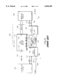
- FIG. 1 illustrates a block diagram of an exemplary FIFO buffer between two digital systems which has a write controller synchronized to a first clock signal and which has a read controller synchronized to a second clock signal wherein the two clock signals are mutually asynchronous to each other;
- FIG. 2 illustrates a block diagram of the write controller and the read controller of FIG. 1 which incorporate synchronization circuits in accordance with the present invention between the write controller and the read controller;
- FIG. 3 illustrates a logic diagram of the synchronization circuit in accordance with the present invention which synchronizes the transfer of the pointer values between the write address controller and the read address controller in FIG. 2;
- FIG. 4 (comprising FIGS. 4A-4N) illustrates timing diagrams for the synchronization circuit of FIG. 3;
- FIG. 5 illustrates a logic diagram of the synchronization circuit in accordance with the present invention which synchronizes the transfer of the pointer values between the read address controller and the write address controller in FIG. 2;
- FIG. 6 illustrates a logic diagram of an alternative synchronization circuit in which a single synchronization logic circuit synchronizes the transfer of the pointer values between the write address controller and the read address controller and also synchronizes the transfer of pointer values between the read address controller and the write address controller.
- FIG. 1 illustrates a block diagram of an exemplary FIFO (first-in/first-out) buffer 100 between a transmitting circuit 102 and a receiving circuit 104.
- the transmitting circuit 102 represents the data output interface of a source of digital data, such as, for example, a computer system or the like
- the receiving circuit 104 represents a data input interface of a destination for the digital data, such as, for example, a mass storage device such as a disk drive, a tape drive, or the like.
- a computer system and a mass storage device typically transfer data bidirectionally such that both the computer system and the mass storage device can operate as either a source or a destination for data.
- the description herein is thus not limited to a system for transferring data between a computer system and a data storage device.
- the present invention also can be used to control transmission of data between any data source and any data destination.
- the transmitting circuit 102 operates in synchronism with a first clock signal (CLOCK1) on a first clock signal line 106
- the receiving circuit 104 operates in synchronism with a second clock signal (CLOCK2) on a second clock signal line 108.
- the two clock signals operate asynchronously with respect to each other and may have substantially different frequencies.
- the transmitting circuit 102 and the receiving circuit 104 may operate in different transfer modes.
- the transmitting circuit 102 may generate data at a data rate that has no fixed relationship with the rate at which the receiving circuit 104 is able to accept the data.
- the transmitting circuit 102 may generate the data in bursts of multiple units of data while the receiving circuit 104 receives the data at a relatively constant rate, or, conversely, the transmitting circuit 102 may generate the data at a relatively constant rate while the receiving circuit 104 receives the data in bursts.
- a unit of data is the amount of data which can be transmitted from the transmitting circuit 102 at one time.
- the unit of data (or data unit) may be, for example, a byte (eight bits), a word (two bytes), a double word (four bytes), a nibble (four bits), a single bit, or the like.
- the FIFO buffer 100 is used to allow the transmitting circuit 102 to operate in synchronism with its respective clock (CLOCK1) and to transfer data using its transfer mode.
- the FIFO buffer 100 also allows the receiving circuit 104 to operate in synchronism with its respective clock (CLOCK2) and to transfer data using its transfer mode.
- the FIFO buffer 100 comprises a two-port FIFO buffer memory 110 which comprises a data input port 112 and a data output port 114.
- the data input port 112 comprises a data input (DI) bus 120, a write address (WA) bus 122 and a write control or write enable (WE) signal input 124.
- DI data input
- WA write address
- WE write control or write enable
- the data output port comprises a data output (DO) bus 130, a read address (RA) bus 132 and an output enable (OE) signal input 134.
- the data input port 112 is controlled by a write controller 140.
- the data output port 114 is controlled by a read controller 142.
- the transmitting circuit 102 generates an active data ready signal (RDY) on a data ready signal line 150 to the write controller 140 whenever the transmitting circuit 102 has a unit of data ready to be transferred. If the FIFO buffer memory 110 has an available data storage location, the write controller 140 applies the next available address to the write address bus 122 of the FIFO buffer memory 110 and activates the write enable signal on the signal line 124 to store the data in the addressed memory location. The write controller 140 then activates an acknowledge (ACK) signal on an acknowledge signal line 152 to indicate to the transmitting circuit 102 that the data unit has been stored in the FIFO buffer memory 110. If the transmitting circuit has additional data units to transfer, the transmitting circuit 102 again activates the ready signal on the data ready signal line 150, and the process is repeated.
- RDY active data ready signal
- the read controller 142 If the FIFO buffer memory 110 contains a data unit to be transferred to the receiving circuit 104, the read controller 142 generates an active data ready signal (RDY) on a data ready signal line 160 to the receiving circuit 104 and activates the output enable signal on the signal line 134 to cause the data unit stored at the location addressed by the current value on the read address bus 132 to be output on the read data bus 130.
- the receiving circuit 104 indicates that the data unit has been accepted by activating an acknowledge signal (ACK) on an acknowledge signal line 162. If additional data units are stored in the FIFO buffer memory 110 to be transferred to the receiving circuit 104, the above-described process is repeated.
- the write controller 140 includes a write address counter 170 which generates a write address pointer which keeps track of the current storage location within the FIFO buffer memory 110 to which to transfer a data unit to be stored.
- the write address pointer is provided to the write address input of the FIFO buffer memory 110 via the write address bus 122.
- the write address counter 170 is incremented to the next count value to point to the next storage location in the FIFO buffer memory 110.
- the FIFO buffer memory 110 is operated as a circular memory
- the write address counter 170 is a modulo counter having a maximum count value corresponding to the highest storage location address of the FIFO buffer memory 110 such that when the maximum count value of the write address counter 170 is reached, the next count value is a value corresponding to the lowest storage location address of the FIFO buffer memory 110.
- the read controller 142 includes a read address counter 172 which generates a read address pointer which keeps track of the current storage location within the FIFO buffer memory 110 from which to transfer a data unit to be read.
- the read address pointer is provided to the read address input of the FIFO buffer memory 110 via the read address bus 132.
- the read address counter 172 is incremented to the next count value to point to the next storage location in the FIFO buffer memory 110.
- the read address counter 172 is also a modulo counter which changes to its lowest value when incremented from its maximum value.
- the write controller 140 In addition to controlling the write address counter 170, the write controller 140 must also monitor the value of the read address counter 172 in the read controller 142. Because the rate at which data units are read from the FIFO buffer memory 110 may be considerable slower than the rate at which the data units are stored in the FIFO buffer memory 110, it is possible that the write address counter 170 can be incremented to a value that corresponds to a data storage location into which a data unit has been stored but which has not yet been transferred out to the receiving circuit 104. By monitoring the value of the read address counter 172 and comparing it to the value of the write address counter 170, the write controller 140 can determine when the next addressed data storage location in the FIFO buffer memory 110 has not been read since the last write operation. The write controller 140 will thus inhibit the acknowledge signal on the ACK line 152 so that the data transfer from the transmitting circuit 102 is not acknowledged until the value of the read address counter 172 is incremented and the data storage location becomes available.
- the read controller 142 can determine when it has transferred all the data units currently stored in the FIFO buffer memory 110 and will stop transferring data to the receiving circuit 104 until the write address counter 170 is again incremented to indicate that a new data unit has been stored in the FIFO buffer memory 110.
- a number of different comparison systems can be used by the write control circuit 140 and the read control circuit 142. Detailed descriptions of the comparison circuits in the write address controller 140 and the read address controller 142 are not necessary to the understanding of the present invention which will be described in detail below.
- the write address controller 140 it is necessary for the write address controller 140 to monitor the output of the read address counter 172 in order to avoid overwriting unread data units in data storage locations, and it is necessary for the read address controller 142 to monitor the output of the write address counter 170 to avoid reading data units from data storage locations from which the data units have already been transferred. Because the write address controller 140 and the read address controller 142 are operating in synchronism with mutually asynchronous clock signals (CLOCK1 and CLOCK2, respectively), the write address counter 170 may be updated at unpredictable times with respect to the phases of the CLOCK2 signal which controls the read address controller 142. Similarly, the read address counter 172 may be updated at unpredictable times with respect to the phases of the CLOCK1 signal which controls the operation of the write address controller 140.
- the write address controller 140 simply latches the output of the read address counter 172 in synchronism with CLOCK1, the latching operation may occur just as the read address counter 172 is being incremented.
- the results of such a latching operation will often result in a value that does not correspond to either the value before the read address counter 172 was incremented or the value after the read address counter 172 was incremented.
- the read address counter 172 comprises eight bits which increment from all zeros (i.e., 00000000) to all ones (i.e., 11111111) and then change back to all zeros when the next increment operation occurs, during a relatively short transition time when the count value changes from all ones to all zeros, some of the ones will change to zeros before others of the ones change to zeros. If the write controller 140 latches the read address pointer output of the read address counter 172 during this transition time, the actual value latched by the write controller 140 is unpredictable. A similar unpredictable result could occur if the write address pointer value is latched by the read controller 142 when the write address counter 170 is being incremented.
- an improved FIFO buffer 200 in accordance with the present invention includes a first synchronization circuit 210 between the output of the write address counter 170 and the read controller 142 and includes a second synchronization circuit 212 between the output of the read address counter 172 and the write controller 140.
- the first synchronization circuit 210 generates a synchronized write address pointer (SYNCHED WRITE POINTER) on a synchronized write pointer bus 214 which is provided as an input to the read controller 142.
- the synchronized write address pointer on the bus 214 is synchronized with the CLOCK2 signal to assure that the write address value evaluated by the read controller 142 does not change when the comparison is being performed by the read controller 142.
- the second synchronization circuit 212 generates a synchronized read address pointer (SYNCHED READ POINTER) on a synchronized read pointer bus 216 which is provided as an input to the write controller 140.
- the synchronized read address pointer on the bus 216 is synchronized with the CLOCK1 signal to assure that the read address value evaluated by the write controller 140 does not change when the comparison is being performed by the write controller 142.
- FIG. 3 A detailed block diagram of the first synchronization circuit 210 is illustrated in FIG. 3.
- the second synchronization circuit 212 which is substantially similar to the first synchronization circuit 210, is illustrated in FIG. 5.
- An alternative synchronization circuit 216 which combines common elements of the first and second synchronization circuits is illustrated in FIG. 6.
- clock CLOCK1 or CLOCK2
- CLOCK1 or CLOCK2 can have a higher frequency than the other clock.
- the synchronization circuits can be used even if it is not known in advance that one clock will always have a higher frequency.
- the first synchronization circuit 210 comprises an input latch 300 which is a multiple-bit input latch which receives and latches the write address pointer (POINTER IN) generated by the write address counter 170 (FIG. 2) on the bus 122. That is, the input latch 300 provides a temporary data storage location for each bit of the write address pointer.
- the output of the input latch 300 is a multiple-bit signal LATCHED POINTER on a latched pointer bus 302.
- the LATCHED POINTER signal on the bus 302 is provided as an input to an output latch 304 which latches the LATCHED POINTER signal and provides a multiple-bit SYNCHED POINTER OUT signal on the synchronized write address bus 214.
- the input latch 300 and the output latch 304 are controlled by synchronization logic 306 described below.
- the input latch 300 and the output latch 304 are latched registers. That is, data bits provided to the respective data (D) inputs of the latches are passed through the latches and appear at the outputs (Q) of the latches when a respective latch enable signal on a respective latch enable (E) input is active.
- the latch enable signal becomes inactive, the data bits at the data inputs at the time the latch enable signal becomes inactive are latched at the outputs of the respective latch 300, 304 and the output signals do not change irrespective of changes in the signals applied to the inputs of the latches. As illustrated in FIG.
- the input latch enable signal applied to the input latch 300 is clocked in synchronism with the CLOCK1 signal on the first clock signal line 106 to latch the write address pointer into the input latch 300 when the write address pointer is assured to be stable.
- the output latch enable signal applied to the output latch 304 is clocked in synchronism with the CLOCK2 signal on the second clock signal line 108 to assure that the SYNCHED POINTER OUT signal on the bus 214 is stable when compared to the read address pointer which is generated in synchronism with the CLOCK2 signal.
- the synchronization logic 306 operates to control the generation of the input latch enable signal and the output latch enable signal to assure that the data bits of the LATCHED POINTER signal on the bus 302 do not change when the output latch enable signal is active.
- the synchronization logic 306 comprises a clock1-to-clock2 synchronization section 310 and a clock2-to-clock1 synchronization section 312.
- the clock1-to-clock2 synchronization section 310 has an input 314 and an output 316.
- the clock2-to-clock1 synchronization section 312 has an input 318 and an output 320.
- the output 316 of the clock1-to-clock2 synchronization section 310 generates a signal SYNC 1 which is provided to the input 318 of the clock2-to-clock1 synchronization section 312.
- the SYNC1 signal is also provided to the enable (E) input of the output latch 304.
- the output 320 of the clock2-to-clock1 synchronization section 312 generates a signal SYNC2 which is provided to the input 314 of the clock1-to-clock2 synchronization section 310.
- the SYNC2 signal is also provided to the enable (E) input of the input latch 300.
- Both the clock1-to-clock2 synchronization section 310 and the clock2-to-clock1 synchronization section 312 receive the CLOCK1 signal and the CLOCK2 signal.
- the clock1-to-clock2 synchronization section 310 comprises a first D flip-flop 330, a second D flip-flop 332, a third D flip-flop 334 and a fourth D flip-flop 336.
- the clock1-to-clock2 synchronization circuit further includes a first two-input exclusive-OR gate 340 and a second two-input exclusive-OR gate 342.
- Each of the D flip-flops 330, 332, 334, 336 has a respective data (D) input, a respective clock (C) input and a respective data (Q) output.
- the D flip-flops 330, 332, 334, 336 are edge-triggered flip-flops such that the data at the D input is transferred to the Q output when a clock signal applied to the clock (C) input transitions from one logic level to another logic level. Logic levels at the D input at times other than the specified edge (i.e., the specified transition) are ignored. In the embodiment illustrated in FIG. 3, all the D flip-flops are positive edge triggered flip-flops such that the logic level on the D input is transferred in response to a transition of the clock signal from a low logic level to a high logic level. Transitions of the clock signal from a high logic level to a low logic level have no effect.
- the clock input of the first flip-flop 330 receives the CLOCK1 signal and is thus synchronized with the transmitting circuit 102.
- the clock inputs of the second, third and fourth flip-flops 332, 334, 336 receive the CLOCK2 signal and are thus synchronized with the receiving circuit 104.
- a first input of the first exclusive-OR gate 340 is connected to the input 314 of the clock1-to-clock2 synchronization section 310 and thus receives the SYNC2 signal from the clock2-to-clock1 synchronization section 312.
- a second input of the first exclusive-OR gate 340 is connected to the Q output of the first flip-flop 330.
- the signal generated by the Q output of the first flip-flop 330 is referred to herein as TRIG1.
- the output of the first exclusive-OR gate 340 is connected to the D input of the first flip-flop 330.
- the Q output of the first flip-flop 330 is also connected to the D input of the second flip-flop 332.
- the Q output of the second flip-flop 332 is connected to the D input of the third flip-flop 334.
- the Q output of the third flip-flop 334 is connected to the D input of the fourth flip-flop 334 and to a first input of the second exclusive-OR gate 342.
- the Q output of the fourth flip-flop 336 is connected to a second input of the second exclusive-OR gate 342.
- the output of the second exclusive-OR gate 342 is the SYNC1 signal which is provided on the output 316 of the clock1-to-clock2 synchronization section 310 and which is connected to the enable (E) input of the output latch 304 and to the input 318 of the clock2-to-clock1 synchronization section 312.
- the first D flip-flop 330 further includes a preset (PR) input which, in the illustrated embodiment, receives an active low reset (RST1) signal on a first reset bus 344.
- the RST1 signal is synchronized with the CLOCK1 signal.
- the Q output of the first D flip-flop 330 is forced to a high (i.e., logic 1) level irrespective of the logic level on the D input.
- the second, third and fourth D flip-flops 332, 334, 336 further include respective reset (RN) inputs which receive an active low reset (RST2) signal on a second reset bus 346.
- the RST2 signal is synchronized with the CLOCK2 signal.
- the respective Q outputs of the second, third and fourth flip-flops 332, 334, 336 are reset to a low logic level when the RST2 signal is active.
- the Q output of the first flip-flop 330 will be at a logical 1 level and the Q outputs of the second, third and fourth flip-flops 332, 334, 336 will all be at a logical 0 level.
- the clock2-to-clock1 synchronization section 312 is similar to the clock1-to-clock2synchronization section 310.
- the clock2-to-clock1 synchronization section 312 comprises a fifth D flip-flop 350, a sixth D flip-flop 352, a seventh D flip-flop 354 and an eighth D flip-flop 356.
- the clock1-to-clock2 synchronization section 312 further includes a third two-input exclusive-OR gate 370 and a fourth two-input exclusive-OR gate 372.
- Each of the D flip-flops 350, 352, 354, 356 has a respective data (D) input, a respective clock (C) input and a respective data (Q) output.
- the D flip-flops 350, 352, 354, 356 are positive edge-triggered flip-flops which operate as described above.
- the clock input of the fifth flip-flop 350 receives the CLOCK2 signal and is thus synchronized with the receiving circuit 104.
- the clock inputs of the sixth, seventh and eighth flip-flops 352, 354, 356 receive the CLOCK1 signal and are thus synchronized with the transmitting circuit 102.
- a first input of the third exclusive-OR gate 370 is connected to the input 318 of the clock2-to-clock1 synchronization section 312 and thus receives the SYNC1 signal from the clock1-to-clock2 synchronization section 310.
- a second input of the third exclusive-OR gate 370 is connected to the Q output of the fifth flip-flop 350.
- the signal generated by the Q output of the fifth flip-flop 350 is referred to herein as TRIG2.
- the output of the third exclusive-OR gate 370 is connected to the D input of the fifth flip-flop 350.
- the Q output of the fifth flip-flop 350 is also connected to the D input of the sixth flip-flop 352.
- the Q output of the sixth flip-flop 352 is connected to the D input of the seventh flip-flop 354.
- the Q output of the seventh flip-flop 354 is connected to the D input of the eighth flip-flop 356 and to a first input of the fourth exclusive-OR gate 372.
- the Q output of the eighth flip-flop 356 is connected to a second input of the fourth exclusive-OR gate 372.
- the output of the fourth exclusive-OR gate 372 is the SYNC2 signal which is provided on the output 320 of the clock2-to-clock1 synchronization section 312 and which is connected to the enable (E) input of the input latch 302 and to the input 314 of the clock1-to-clock2 synchronization section 310.
- the fifth D flip-flop 350 further includes a reset (RN) input which, in the illustrated embodiment, receives the active low reset (RST2) signal on the second reset bus 346.
- RST2 active low reset
- the sixth, seventh and eighth D flip-flops 352, 354, 356 further include respective reset (RN) inputs which receive the active low reset (RST1) signal on the first reset bus 344.
- FIGS. 4A-4N The operation of the synchronization logic 306 is illustrated by the timing diagrams in FIGS. 4A-4N.
- FIG. 4A illustrates a timing waveform 400 for the CLOCK1 signal.
- FIG. 4B illustrates a timing waveform 402 for the CLOCK2 signal.
- the CLOCK2 signal has a lower frequency than the CLOCK1 signal and is asynchronous with the CLOCK1 signal.
- FIG. 4C illustrates a timing waveform 404 for the first reset signal RST1.
- the first reset signal is initially at an active low logic level to preset the Q output of the first flip-flop 330 to a logical one and to reset the sixth, seventh and eighth flip-flops 352, 354, 356 to logical zeros.
- the first reset signal changes to an inactive high level via a low-to-high transition 406 which is preferably synchronized with the CLOCK1 signal.
- FIG. 4D illustrates a timing waveform 410 for the second reset signal RST2.
- the second reset signal is initially at an active low logic level to reset the Q outputs of the second, third, fourth and fifth flip-flops 332, 334, 336, 350 to logical zeros.
- the second reset signal changes to an inactive high level via a low-to-high transition 412 which is preferably synchronized with the CLOCK2 signal.
- FIG. 4E illustrates a timing waveform 420 for the first trigger signal (TRIG1) which corresponds to the Q output of the first flip-flop 330.
- the TRIG1 signal is preset to a logical one by the first reset signal and remains at a logical one until changed by the SYNC2 signal as will be described below.
- the TRIG1 signal at the beginning of each cycle of the CLOCK1 signal corresponds to the exclusive-OR of the TRIG1 signal and the SYNC2 signal (shown in FIG. 4N).
- the output of the first exclusive-OR gate 340 will be a constant logical one until the SYNC2 signal changes.
- FIG. 4F illustrates a timing waveform 422 for the Q output of the second flip-flop 332 and is identified as Q332.
- the Q332 signal is initially reset to a logical zero by the second reset signal and remains at a logical zero until the second reset signal becomes inactive.
- the second reset signal preferably changes from its active low state to its active high state in synchronism with the CLOCK2 signal.
- the logic level at the data input of the second flip-flop 332 will be transferred to the Q output of the second flip-flop 332 as the Q332 signal.
- the Q332 signal makes a low-to-high transition 424. As illustrated, the Q332 signal remains at a logical one level until the TRIG1 signal changes in accordance with the following description.
- FIG. 4G illustrates a timing waveform 430 for the Q output of the third flip-flop 334 and is identified as Q334.
- the Q334 signal is initially reset to a logical zero by the second reset signal.
- the Q334 signal remains at a logical zero until one CLOCK2 cycle after the transition 424 of the Q332 signal.
- the Q334 signal makes a low-to-high transition 432.
- the Q334 signal remains at a logical one until one CLOCK2 cycle after the Q332 signal next changes, as described below.
- FIG. 4H illustrates a timing waveform 440 for the Q output of the fourth flip-flop 336 and is identified as Q336.
- the Q336 signal is initially reset to a logical zero by the second reset signal and remains at a logical zero one CLOCK2 cycle after the transition 432 of the Q334 signal.
- the Q336 signal makes a low-to-high transition 442.
- the Q336 signal remains at a logical one until one clock cycle after the Q334 signal next changes, as described below.
- FIG. 4I illustrates a timing waveform 450 for the SYNC1 signal on the output of the second exclusive-OR gate 342.
- the SYNC1 signal is the exclusive-OR of the Q334 signal and the Q336 signal.
- the SYNC1 signal makes an low-to-high transition 452 when the Q334 signal makes the transition 432 such that the Q334 signal and the Q336 signal have different logic levels.
- the SYNC1 signal then makes a high-to-low transition 454 when the Q336 signal makes the transition 442 on the next positive edge of the CLOCK2 signal and the Q334 signal and the Q336 signal again have the same logic level.
- the SYNC1 signal makes a low-to-high-to-low sequence in one cycle of the CLOCK2 signal.
- the SYNC1 signal enables the output latch 304 when the SYNC1 signal has a high logic level.
- the pointer data on the latched pointer bus 302 pass through the output latch 304 to the output bus 214 during the time interval between the transition 452 and the transition 454.
- the pointer data remain latched in the output latch 304 and are thus stable on the output bus 214 until the SYNC1 signal again makes a low-to-high transition, as discussed below.
- FIG. 4J illustrates a timing waveform 460 for the TRIG2 signal on the Q output of the fifth flip-flop 350.
- the SYNC1 signal and the TRIG2 signal are both provided as inputs to the third exclusive-OR gate 370.
- the output of the third exclusive-OR gate 370 is the data input to the fifth flip-flop 350.
- the new value for the TRIG2 signal is the exclusive-OR of the previous value of the TRIG2 signal and the previous value of the SYNC1 signal.
- the output of the third exclusive-OR gate 370 will switch to a logical one because the SYNC1 signal has a different logic level than the TRIG2 signal.
- the TRIG2 signal makes a low-to-high transition 462 as the SYNC1 signal makes the high-to-low transition 454.
- the SYNC1 signal and the TRIG2 signal again have mutually different logic levels, and the TRIG2 signal remains at a logic one level.
- the TRIG2 signal changes logic levels at the same time that the SYNC1 signal switches back to the low logic level.
- the TRIG2 signal then remains at the new logic level until the end of the next low-to-high-to-low sequence of the SYNC1 signal.
- the operation of the clock2-to-clock1 synchronization section 312 is illustrated by a Q352 waveform 470 in FIG. 4K, a Q354 waveform 472 in FIG. 4L, a Q356 waveform 474 in FIG. 4M and a SYNC2 waveform 476 in FIG. 4N.
- the clock2-to-clock1 synchronization section 312 operates in a similar manner to the clock1-to-clock2 synchronization section 310 as described above.
- the high logic level which results from the low-to-high transition 462 of the TRIG2 signal (which occurs in the CLOCK2 clock domain) is detected at the data input of the sixth flip-flop 352 on the next positive edge of the CLOCK1 signal to cause a low-to-high transition 480 of the Q352 signal.
- the resulting high logic level of the Q352 signal causes a low-to-high transition 482 of the Q354 signal on the next positive edge of the CLOCK1 signal.
- the resulting high logic level of the Q354 signal causes a low-to-high transition 484 of the Q356 signal on the next positive edge of the CLOCK1 signal.
- the Q354 signal and the Q356 signal are provided as the two inputs to the fourth exclusive-OR gate 372.
- both signals are at logical zero levels.
- the SYNC2 signal 476 generated on the output of the fourth exclusive-OR gate 370 is a logical zero.
- the Q354 signal makes the low-to-high transition 482
- the Q354 signal is at a different logic level for one cycle of the CLOCK1 signal until the Q356 signal makes the low-to-high transition 484 and also becomes a logical one.
- the SYNC2 output of the fourth exclusive-OR gate 372 makes a low-to-high transition 486 in response to the low-to-high transition 482 of the Q354 signal and remains at a logical one for one clock cycle while the two signals have different logic levels and then returns to a logical zero via a high-to-low transition 488 in response to the low-to-high transition 484 of the Q356 signal when both the Q354 signal and the Q356 signal again have the same logic level.
- the POINTER IN data on the input data bus 122 at the input of the input latch 300 are propagated through the input latch 300 to the output of the input latch 300 and thus to the latched pointer bus 302.
- the SYNC2 signal makes the transition 488 back to the low logic level the data on the output of the input latch 300 are latched such that further changes to the data on POINTER IN data bus 122 have no effect on the output data.
- the high logic level on the SYNC2 signal is provided to the input of the first exclusive-OR gate 340. Because the other input of the exclusive-OR gate 340 is the TRIG1 signal, which, as shown in FIG. 4E, is also at a high logic level, the output of the first exclusive-OR gate 340 switches to a low logic level. Thus, on the next positive edge of the CLOCK1 signal, the TRIG1 signal on the Q output of the first flip-flop 350 makes a high-to-low transition 500 to a low logic level. At the same time, the SYNC2 signal has also made the high-to-low transition 488. Thus, because the logic levels of both inputs to the first exclusive-OR gate 340 are equal to each other, the output of the first exclusive-OR gate 340 remains at a low logic level after the transitions 488, 500.
- the low logic level of the TRIG1 signal causes the Q332 signal to make a high-to-low transition 510 on the next positive edge of the CLOCK2 signal.
- the Q334 signal makes a high-to-low transition 512 on the next positive edge of the CLOCK2 signal.
- the Q336 signal makes a high-to-low transition 514 on the next positive edge of the CLOCK2 signal.
- the two inputs of the second exclusive-OR gate 342 are again different causing the SYNC1 output of the second exclusive-OR gate 342 to make a low-to-high transition 520 to a logical one.
- the two inputs of the second exclusive-OR gate 342 have the same logic level and the output of the second exclusive-OR gate 342 makes a high-to-low transition 522 to a logical zero.
- the active high SYNC1 signal causes the output latch 304 to gate the latched pointer data on the LATCHED POINTER bus 302 through to the SYNCHED POINTER OUT bus 214.
- the pointer data which were gated onto the LATCHED POINTER bus 302 from the POINTER IN bus 122 in synchronism with the CLOCK1 signal are gated out to the SYNCHED POINTER OUT bus 214 in synchronism with the CLOCK2 signal. Because the pointer data are gated onto the LATCHED POINTER bus 302 in synchronism with the CLOCK1 signal from the transmitting circuit 102, there is no possibility that the data can be unstable when gated onto the bus 302.
- the pointer data are gated from the bus 302 to the receiving circuit 104 in synchronism with the CLOCK2 signal which controls the receiving circuit 104, there is no possibility that the data transferred to the receiving circuit are unstable. It should be further noted that the data are guaranteed to be stable on the LATCHED POINTER bus 302 before the output latch 304 gates the data from the bus 302 because the second flip-flop 332 imposes at least one full cycle of the CLOCK2 signal before the SYNC2 signal enables the output latch 304.
- the second flip-flop 332 further operates to preclude any metastability condition from causing glitches in the SYNC1 signal.
- the second flip-flop 332 receives the TRIG1 signal which changes in synchronism with the CLOCK1 signal.
- the second flip-flop 332 is clocked by the CLOCK2 signal, which is asynchronous to the CLOCK1 signal.
- the TRIG1 signal will change (i.e., have a transition) at approximately the same time that the TRIG1 signal is clocked into the second flip-flop 332.
- the Q output of the second flip-flop 332 may exhibit a metastable condition. That is, the Q output may oscillate between its two possible logic levels for a short interval before stabilizing in one of the logic levels. If the metastable signal were to be applied to the second exclusive-OR gate 342, it is possible to generate multiple active high SYNC1 signals rather than one single pulse as illustrated in FIG. 4I.
- the metastable condition will end within one cycle of the CLOCK2 signal, and thus the Q332 signal presented to the data input of the third flip-flop 334 at the time of the next positive edge of the CLOCK2 signal will be stable and the Q334 signal on the output of the third flip-flop 334 will likewise be stable. Note that if the metastable condition terminates with the Q332 signal at a logic level different than the logic level of the TRIG1 signal, the TRIG1 signal will be guaranteed to satisfy the setup and hold times of the second flip-flop 332 on the next positive edge of the CLOCK2 signal. If this event occurs, the only effect of the metastable condition is to add a delay equivalent to an extra cycle of the CLOCK2 signal before the Q334 signal makes the transition 512 (or the transition 432 described above).
- the SYNC1 signal between the low-to-high transition 520 and the high-to-low transition 522 is provided to the third exclusive-OR gate 370 as discussed above; however, because the TRIG2 signal is at a high logic level this time, the two high logic levels causes the output of the third exclusive-OR 370 to transition to a logic zero, and thus, on the next positive edge of the CLOCK2 signal, the TRIG2 signal will make a high-to-low transition 530. The TRIG2 signal will then remain at the low logic level because the SYNC1 signal will also be at a low logic level on the next positive edge of the CLOCK2 signal.
- the Q352 signal makes a high-to-low transition 532. Then, on the next positive transition of the CLOCK1 signal, the Q354 signal makes a low-to-high transition 534 (or, if a temporary metastable condition occurs, the transition 534 will be delayed by an additional cycle of the CLOCK1 signal). On the next positive edge of the CLOCK1 signal following the transition 534, the Q356 signal will make a high-to-low transition 536.
- the Q354 signal and the Q356 signal have different logic levels between the transition 534 of the Q354 signal and the transition 536 of the Q356 signal.
- the TRIG2 signal on the output of the fourth exclusive-OR gate 372 will make a low-to-high transition 540 in response to the transition 534 and will make a high-to-low transition 542 in response to the transition 536.
- the SYNC2 signal will again be active for one cycle of the CLOCK2 signal to gate the current value on the POINTER IN bus 122 through the input latch 300 to the LATCHED POINTER bus 302.
- the SYNC2 signal causes the TRIG1 signal to make a low-to-high transition 544 on the next positive transition of the CLOCK1 signal, and the TRIG1 signal causes the Q332 signal to make a low-to-high transition 546 on the next positive transition of the CLOCK2 signal.
- the first latch enable pulse generated by the synchronization circuit 210 after being released from the reset condition is the active high SYNC1 signal between the transition 452 and the transition 454 which enables the output latch 304.
- the initial contents of the LATCHED POINTER bus 302 may be uncertain because the input latch 300 has not yet been enabled.
- the input latch 300 includes a reset (RN) input which receives the first reset signal RST1.
- RST1 reset signal
- the input latch 300 can be enabled first by causing the fifth flip-flop 350 to be preset and the first flip-flop 330 to be reset so that the first active enable signal to be generated is the SYNC2 signal input to the input latch 300.
- the synchronization logic 306 alternately generates SYNC2 synchronization pulses which gate the pointer data onto the bus 302 in synchronization with the CLOCK1 signal and SYNC1 synchronization pulses which gate the pointer data from the bus 302 to the output bus 214 in synchronization with the CLOCK2 signal.
- the clock1-to-clock2 synchronization section 310 assures that the pointer data placed on the bus 302 in the CLOCK1 signal domain are stable in the CLOCK2 signal domain before the data are transferred from the bus 302.
- the clock2-to-clock1 synchronization section 312 assures that the pointer data have been transferred from the bus 302 to the bus 214 in the CLOCK2 signal domain before permitting the next pointer data to be placed on the bus 302 in the CLOCK1 signal domain.
- the read controller 142 cannot monitor every change in the pointer value. Basically, the read controller 142 only monitors the write address pointer whenever it is ready to read data to verify that the data to read is current. As long as the write address pointer monitored by the read controller 142 is less than or equal to the current write address pointer of the write controller 140, the read controller 142 will not attempt to read previously read data.
- the present invention precludes the read controller 142 from misreading the write address pointer by assuring that the write address pointer is always stable in the CLOCK2 signal domain.
- the synchronization circuit 210 illustrated in FIG. 3 synchronizes the write address pointer being transferred from the CLOCK1 signal domain to the CLOCK2 signal domain.
- FIG. 5 illustrates the synchronization circuit 212 for synchronizing the transfer of the read address pointer from the CLOCK2 signal domain to the CLOCK1 signal domain.
- An input latch 300B gates the read pointer input from the READ POINTER bus 132 to a LATCHED POINTER bus 302B in synchronism with the CLOCK2 signal.
- An output latch 304B gates the latched signal to the SYNCHED READ POINTER OUT bus 216 in synchronism with the CLOCK1 signal.
- the synchronization is controlled by synchronization logic 306B which comprises a clock2-to-clock1 synchronization section 310B which corresponds to the clock1-to-clock2 synchronization section 310 of FIG. 3 and comprises like numbered flip-flops 330, 332, 334, 336 and exclusive-OR gates 340, 342.
- the synchronization logic 306B further comprises a clock1-to-clock2synchronization section 312B which corresponds to the clock2-to-clock1 synchronization section 312 of FIG.
- FIG. 3 and comprises like numbered flip-flops 350, 352, 354, 356 and exclusive-OR gates 370, 372.
- the operation of the two synchronization sections 310B, 312B in synchronously transferring pointer values from one clock domain to the other clock domain has been described above in connection with FIGS. 3 and 4 except that in FIG. 5, the pointer values are transferred from the CLOCK2 domain to the CLOCK1 domain and the clock signals and reset signals controlling the flip-flops have been interchanged in FIG. 5 with respect to FIG. 3.
- the input latch 300B, the first flip-flop 330, the sixth flip-flop 352, the seventh flip-flop 354 and the eighth flip-flop 356 receive the CLOCK2 signal and the second reset signal RST2, and thus operate in the CLOCK2 domain.
- the output latch 302B, the second flip-flop 332, the third flip-flop 334, the fourth flip-flop 336 and the fifth flip-flop 350 receive the CLOCK1 signal and the first reset signal RST1, and thus operate in the CLOCK1 domain.
- the second synchronization circuit 212 operates as described above for the first synchronization circuit 210 except that data are gated to the LATCHED POINTER bus 302 in synchronism with the CLOCK2 signal and are gated from the LATCHED POINTER bus 302 to the SYNCHED READ POINTER OUT bus 216 in synchronism with the CLOCK1 signal.
- FIG. 6 illustrates a further alternative embodiment in which the transfer of the write address pointer and the transfer of the read address pointer are controlled by common synchronization logic for the transfer of pointer values in both directions.
- a synchronization circuit 600 in FIG. 6 includes a lower portion which corresponds to the synchronization circuit 210 of FIG. 3 to transfer the write address pointer from the CLOCK1 signal domain to the CLOCK2 signal domain as described above. The write address pointer propagates from left to right in FIG.
- the latched write pointer on the LATCHED POINTER bus 302 is gated through a first output latch 304 to the SYNCHED WRITE POINTER OUT bus 214 in synchronism with the CLOCK2 signal.
- the second input latch 300B, the second LATCHED POINTER bus 302B and the second output latch 304B from FIG. 5 are included to transfer the read address pointer from right to left in FIG. 6.
- the read address pointer in the CLOCK2 signal domain is transferred from the read pointer bus 132 through the second input latch 300B to the second LATCHED POINTER bus 302B in synchronism with the CLOCK2 signal.
- the latched read pointer is transferred from the second LATCHED POINTER bus 302B through the second output latch 304B to the SYNCHED READ POINTER OUTPUT bus 216 in synchronism with the CLOCK1 signal.
- the reset (RN), latch enable (E) and clock inputs of the second input latch 304B are connected to the corresponding inputs of the first output latch 302.
- the reset (RN), latch enable (E) and clock inputs of the second output latch 304 are connected to corresponding inputs of the first input latch 300A.
- the SYNC1 signal and the SYNC2 signal of the single synchronization circuit 600 in FIG. 6 operate to control both sets of latches in the manner controlled separately by the embodiments of FIGS. 3 and 5.
Abstract
Description
Claims (4)
Priority Applications (1)
| Application Number | Priority Date | Filing Date | Title |
|---|---|---|---|
| US08/971,387 US6055285A (en) | 1997-11-17 | 1997-11-17 | Synchronization circuit for transferring pointer between two asynchronous circuits |
Applications Claiming Priority (1)
| Application Number | Priority Date | Filing Date | Title |
|---|---|---|---|
| US08/971,387 US6055285A (en) | 1997-11-17 | 1997-11-17 | Synchronization circuit for transferring pointer between two asynchronous circuits |
Publications (1)
| Publication Number | Publication Date |
|---|---|
| US6055285A true US6055285A (en) | 2000-04-25 |
Family
ID=25518318
Family Applications (1)
| Application Number | Title | Priority Date | Filing Date |
|---|---|---|---|
| US08/971,387 Expired - Lifetime US6055285A (en) | 1997-11-17 | 1997-11-17 | Synchronization circuit for transferring pointer between two asynchronous circuits |
Country Status (1)
| Country | Link |
|---|---|
| US (1) | US6055285A (en) |
Cited By (71)
| Publication number | Priority date | Publication date | Assignee | Title |
|---|---|---|---|---|
| US6260152B1 (en) * | 1998-07-30 | 2001-07-10 | Siemens Information And Communication Networks, Inc. | Method and apparatus for synchronizing data transfers in a logic circuit having plural clock domains |
| US20010016885A1 (en) * | 1998-06-17 | 2001-08-23 | Aki Happonen | Interface apparatus for connecting devices operating at different clock rates, and a method of operating the interface |
| WO2001079987A1 (en) * | 2000-04-17 | 2001-10-25 | Italtel S.P.A. | Two clock domain pulse to pulse synchronizer |
| US20010038633A1 (en) * | 2000-02-29 | 2001-11-08 | Iain Robertson | Communications interface between clock domains with minimal latency |
| EP1164700A1 (en) * | 2001-03-31 | 2001-12-19 | Agilent Technologies, Inc. (a Delaware corporation) | Data flow synchronization |
| US6369614B1 (en) * | 2000-05-25 | 2002-04-09 | Sun Microsystems, Inc. | Asynchronous completion prediction |
| US20020087909A1 (en) * | 2001-01-03 | 2002-07-04 | Hummel Mark D. | Low latency synchronization of asynchronous data |
| US6424189B1 (en) * | 2000-10-13 | 2002-07-23 | Silicon Integrated Systems Corporation | Apparatus and system for multi-stage event synchronization |
| US20020120796A1 (en) * | 2000-08-17 | 2002-08-29 | Iain Robertson | Maintaining remote queue using two counters in transfer controller with hub and ports |
| US6470459B1 (en) * | 1999-11-29 | 2002-10-22 | Texas Instruments Incorporated | Half-word synchronization method for internal clock |
| US20030052886A1 (en) * | 2000-06-28 | 2003-03-20 | Naegle Nathaniel D. | Transferring a digital video stream through a series of hardware modules |
| US6578093B1 (en) * | 2000-01-19 | 2003-06-10 | Conexant Systems, Inc. | System for loading a saved write pointer into a read pointer of a storage at desired synchronization points within a horizontal video line for synchronizing data |
| US6581165B1 (en) * | 2000-01-14 | 2003-06-17 | Applied Micro Circuits Corporation | System for asynchronously transferring timed data using first and second clock signals for reading and writing respectively when both clock signals maintaining predetermined phase offset |
| US20030123588A1 (en) * | 2002-01-02 | 2003-07-03 | Rupal Parikh | Synchronizing data or signal transfer across clocked logic domains |
| US20030159081A1 (en) * | 2001-12-13 | 2003-08-21 | Maclellan Christopher S. | Data transmission across asynchronous clock domains |
| US6629251B1 (en) * | 1999-10-20 | 2003-09-30 | Applied Micro Circuits Corporation | Elastic store circuit with vernier clock delay |
| US20030206454A1 (en) * | 2002-01-30 | 2003-11-06 | Hernandez Adrian M. | Circuit and method for synchronizing multiple digital data paths |
| US6665807B1 (en) * | 1998-09-04 | 2003-12-16 | Hitachi, Ltd. | Information processing apparatus |
| US6696854B2 (en) * | 2001-09-17 | 2004-02-24 | Broadcom Corporation | Methods and circuitry for implementing first-in first-out structure |
| US6725388B1 (en) * | 2000-06-13 | 2004-04-20 | Intel Corporation | Method and system for performing link synchronization between two clock domains by inserting command signals into a data stream transmitted between the two clock domains |
| US20040088596A1 (en) * | 2002-10-30 | 2004-05-06 | Adc Dsl Systems, Inc. | Method and apparatus for synchronous loading and out-of-phase unloading of data registers |
| US6747997B1 (en) * | 2000-06-13 | 2004-06-08 | Intel Corporation | Network channel receiver architecture |
| US20040111542A1 (en) * | 2002-12-02 | 2004-06-10 | Hiroyasu Noda | Extending circuit for memory and transmitting-receiving device using extending circuit for memory |
| WO2004057487A2 (en) * | 2002-12-20 | 2004-07-08 | Picochip Designs Limited | Array synchronisation |
| US20040205369A1 (en) * | 2003-04-10 | 2004-10-14 | International Business Machines Corporation | Method system and synchronization circuit for providing hardware component access to a set of data values without restriction |
| US20040209587A1 (en) * | 2000-06-12 | 2004-10-21 | Broadcom Corporation | Wireless data communications using FIFO for synchronization memory |
| US6810454B2 (en) | 1998-09-04 | 2004-10-26 | Renesas Technology Corp. | Information processing apparatus having a bus using the protocol of the acknowledge type in the source clock synchronous system |
| US20040251932A1 (en) * | 2003-06-10 | 2004-12-16 | James Ma | Transfer of digital data across asynchronous clock domains |
| US20040251944A1 (en) * | 2003-06-10 | 2004-12-16 | James Ma | Prevention of metastability in bistable circuits |
| US6885217B2 (en) * | 2002-06-20 | 2005-04-26 | Oki Electric Industry Co., Ltd. | Data transfer control circuitry including FIFO buffers |
| US6977897B1 (en) * | 2000-05-08 | 2005-12-20 | Crossroads Systems, Inc. | System and method for jitter compensation in data transfers |
| US20060159209A1 (en) * | 2005-01-18 | 2006-07-20 | Hung-Yuan Hsu | Multi-pipe synchronizer system |
| US20060198479A1 (en) * | 2005-03-01 | 2006-09-07 | Hung-Yuan Hsu | Data synchronizer system |
| US7107393B1 (en) * | 2003-03-28 | 2006-09-12 | Xilinx, Inc. | Systems and method for transferring data asynchronously between clock domains |
| US20060221944A1 (en) * | 2005-03-30 | 2006-10-05 | Intel Corporation | Differential delay compensation |
| US20070041264A1 (en) * | 2005-08-17 | 2007-02-22 | Cohen Daniel S | Method and apparatus for synchronizing data between different clock domains in a memory controller |
| US7231539B1 (en) * | 2004-06-03 | 2007-06-12 | Integrated Device Technology, Inc. | Reset circuit for resetting two clock domains |
| US20070139085A1 (en) * | 2005-10-10 | 2007-06-21 | Stmicroelectronics (Research & Development) Limited | Fast buffer pointer across clock domains |
| US20070236254A1 (en) * | 2006-04-05 | 2007-10-11 | Alcatel | Zero clock delay metastability filtering circuit |
| US20070280396A1 (en) * | 2006-05-31 | 2007-12-06 | Broadcom Corporation | Method and system for advance high performance bus synchronizer |
| US7310396B1 (en) | 2003-03-28 | 2007-12-18 | Xilinx, Inc. | Asynchronous FIFO buffer for synchronizing data transfers between clock domains |
| US7352836B1 (en) * | 2001-08-22 | 2008-04-01 | Nortel Networks Limited | System and method of cross-clock domain rate matching |
| US20080172540A1 (en) * | 2007-01-11 | 2008-07-17 | International Business Machines Corporation | Asynchronous data interface |
| US20080195774A1 (en) * | 2007-01-11 | 2008-08-14 | Lemke Scott J | Structure for an asynchronous data interface |
| US20080201499A1 (en) * | 2005-07-22 | 2008-08-21 | Nxp B.V. | Asynchronous Data Buffer |
| US20080288805A1 (en) * | 2007-05-18 | 2008-11-20 | Advanced Micro Devices, Inc. | Synchronization device and methods thereof |
| US20080307133A1 (en) * | 2006-01-05 | 2008-12-11 | Freescale Semiconductor, Inc. | Method for Synchronizing a Transmission of Information and a Device Having Synchronizing Capabilities |
| US20090149211A1 (en) * | 2007-11-05 | 2009-06-11 | Picochip Designs Limited | Power control |
| US20090172225A1 (en) * | 2004-08-25 | 2009-07-02 | Wiedenman Gregory B | Method and apparatus for providing overlapping defer phase responses |
| US7707448B1 (en) * | 2007-05-03 | 2010-04-27 | Oracle America, Inc. | Deterministic test strand unparking |
| US20110002426A1 (en) * | 2009-01-05 | 2011-01-06 | Picochip Designs Limited | Rake Receiver |
| US7966468B1 (en) * | 2004-12-13 | 2011-06-21 | Nvidia Corporation | Apparatus, system, and method for fast read request transfer through clock domains |
| US8111794B2 (en) * | 2010-04-27 | 2012-02-07 | Kabushiki Kaisha Toshiba | Data synchronizer for synchronizing data and communication interface including the same |
| US8285944B1 (en) * | 2007-01-12 | 2012-10-09 | Xilinx, Inc. | Read-write control of a FIFO memory with packet discard |
| US20130069697A1 (en) * | 2011-09-16 | 2013-03-21 | Lincoln R. Nunes | Synchronizer with high reliability |
| US8463312B2 (en) | 2009-06-05 | 2013-06-11 | Mindspeed Technologies U.K., Limited | Method and device in a communication network |
| US20130254583A1 (en) * | 2011-12-28 | 2013-09-26 | Michael C. Rifani | Data transfer between asynchronous clock domains |
| US8712469B2 (en) | 2011-05-16 | 2014-04-29 | Mindspeed Technologies U.K., Limited | Accessing a base station |
| US8798630B2 (en) | 2009-10-05 | 2014-08-05 | Intel Corporation | Femtocell base station |
| US8849340B2 (en) | 2009-05-07 | 2014-09-30 | Intel Corporation | Methods and devices for reducing interference in an uplink |
| US8862076B2 (en) | 2009-06-05 | 2014-10-14 | Intel Corporation | Method and device in a communication network |
| US8904148B2 (en) | 2000-12-19 | 2014-12-02 | Intel Corporation | Processor architecture with switch matrices for transferring data along buses |
| US9042434B2 (en) | 2011-04-05 | 2015-05-26 | Intel Corporation | Filter |
| US9107136B2 (en) | 2010-08-16 | 2015-08-11 | Intel Corporation | Femtocell access control |
| US20160099031A1 (en) * | 2014-10-07 | 2016-04-07 | Stmicroelectronics S.R.L. | Bi-synchronous electronic device with burst indicator and related methods |
| US20160148661A1 (en) * | 2014-11-24 | 2016-05-26 | Nvidia Corporation | Pausible bisynchronous fifo |
| US20160239263A1 (en) * | 2015-02-13 | 2016-08-18 | Electronics And Telecommunications Research Institute | Dual-clock fifo apparatus for packet transmission |
| US9715914B1 (en) * | 2015-09-26 | 2017-07-25 | Syntropy Systems, Llc | Polyphase buffer for rate-conversion |
| US10856302B2 (en) | 2011-04-05 | 2020-12-01 | Intel Corporation | Multimode base station |
| CN113054996A (en) * | 2021-03-18 | 2021-06-29 | 明峰医疗系统股份有限公司 | Circuit and method for low-delay continuous clock domain crossing inside CT control board |
| US11328755B2 (en) * | 2020-04-03 | 2022-05-10 | Silicon Laboratories Inc. | Data transmission between clock domains for circuits such as microcontrollers |
Citations (27)
| Publication number | Priority date | Publication date | Assignee | Title |
|---|---|---|---|---|
| US4255960A (en) * | 1978-08-25 | 1981-03-17 | Charbonnages De France | Apparatus for measuring and/or monitoring a constituent of an atmosphere |
| US4390969A (en) * | 1980-04-21 | 1983-06-28 | Burroughs Corporation | Asynchronous data transmission system with state variable memory and handshaking protocol circuits |
| US4408333A (en) * | 1981-01-13 | 1983-10-04 | Victor Company Of Japan, Limited | Data acquisition circuit |
| US4498176A (en) * | 1981-02-19 | 1985-02-05 | Siemens Aktiengesellschaft | Method and apparatus for the error-free synchronization of asynchronous pulses |
| US4745302A (en) * | 1985-12-23 | 1988-05-17 | Hitachi, Ltd. | Asynchronous signal synchronizing circuit |
| US4851710A (en) * | 1988-03-29 | 1989-07-25 | Magnetic Peripherals Inc. | Metastable prevent circuit |
| US4866606A (en) * | 1984-06-22 | 1989-09-12 | Austria Miktosystem International Gmbh | Loosely coupled distributed computer system with node synchronization for precision in real time applications |
| US4873703A (en) * | 1985-09-27 | 1989-10-10 | Hewlett-Packard Company | Synchronizing system |
| US4920535A (en) * | 1987-12-14 | 1990-04-24 | Fujitsu Limited | Demultiplexer system |
| US4926445A (en) * | 1987-07-01 | 1990-05-15 | The United States Of America As Represented By The Secretary Of The Air Force | External asynchronous input tester for bit slice machines |
| US4935942A (en) * | 1989-03-16 | 1990-06-19 | Western Digital Corporation | Data sampling architecture |
| US4965465A (en) * | 1988-08-06 | 1990-10-23 | Nec Corporation | Monostable multivibrator capable of generating a predetermined width of pulse without using a delay circuit |
| US4973860A (en) * | 1989-05-02 | 1990-11-27 | Ast Research Inc. | Circuit for synchronizing an asynchronous input signal to a high frequency clock |
| US5012127A (en) * | 1987-09-24 | 1991-04-30 | Ncr Corporation | Synchronizer circuit with asynchronous clearing |
| US5083049A (en) * | 1991-05-10 | 1992-01-21 | Ast Research, Inc. | Asynchronous circuit with edge-triggered inputs |
| US5117442A (en) * | 1988-12-14 | 1992-05-26 | National Semiconductor Corporation | Methods and circuits for synchronizing signals in a modular redundant fault tolerant computer system |
| US5146585A (en) * | 1988-10-25 | 1992-09-08 | International Business Machines Corporation | Synchronized fault tolerant clocks for multiprocessor systems |
| US5155745A (en) * | 1989-10-12 | 1992-10-13 | Nec Corporation | Synchronizer for asynchronous computer command data |
| US5237593A (en) * | 1989-05-04 | 1993-08-17 | Stc, Plc | Sequence synchronisation |
| US5276807A (en) * | 1987-04-13 | 1994-01-04 | Emulex Corporation | Bus interface synchronization circuitry for reducing time between successive data transmission in a system using an asynchronous handshaking |
| US5331669A (en) * | 1992-05-06 | 1994-07-19 | Ologic Corporation | Asynchronous pulse converter |
| US5563891A (en) * | 1995-09-05 | 1996-10-08 | Industrial Technology Research Institute | Waiting time jitter reduction by synchronizer stuffing threshold modulation |
| US5604773A (en) * | 1992-02-14 | 1997-02-18 | Nokia Telecommunications Oy | Desynchronizer and method for suppressing pointer jitter in a desynchronizer |
| US5651034A (en) * | 1992-06-03 | 1997-07-22 | Nokia Telecommunications Oy | Method and equipment for monitoring the fill rate of an elastic buffer memory in a synchronous digital telecommunication system |
| US5729719A (en) * | 1994-09-07 | 1998-03-17 | Adaptec, Inc. | Synchronization circuit for clocked signals of similar frequencies |
| US5905766A (en) * | 1996-03-29 | 1999-05-18 | Fore Systems, Inc. | Synchronizer, method and system for transferring data |
| US5956748A (en) * | 1997-01-30 | 1999-09-21 | Xilinx, Inc. | Asynchronous, dual-port, RAM-based FIFO with bi-directional address synchronization |
-
1997
- 1997-11-17 US US08/971,387 patent/US6055285A/en not_active Expired - Lifetime
Patent Citations (27)
| Publication number | Priority date | Publication date | Assignee | Title |
|---|---|---|---|---|
| US4255960A (en) * | 1978-08-25 | 1981-03-17 | Charbonnages De France | Apparatus for measuring and/or monitoring a constituent of an atmosphere |
| US4390969A (en) * | 1980-04-21 | 1983-06-28 | Burroughs Corporation | Asynchronous data transmission system with state variable memory and handshaking protocol circuits |
| US4408333A (en) * | 1981-01-13 | 1983-10-04 | Victor Company Of Japan, Limited | Data acquisition circuit |
| US4498176A (en) * | 1981-02-19 | 1985-02-05 | Siemens Aktiengesellschaft | Method and apparatus for the error-free synchronization of asynchronous pulses |
| US4866606A (en) * | 1984-06-22 | 1989-09-12 | Austria Miktosystem International Gmbh | Loosely coupled distributed computer system with node synchronization for precision in real time applications |
| US4873703A (en) * | 1985-09-27 | 1989-10-10 | Hewlett-Packard Company | Synchronizing system |
| US4745302A (en) * | 1985-12-23 | 1988-05-17 | Hitachi, Ltd. | Asynchronous signal synchronizing circuit |
| US5276807A (en) * | 1987-04-13 | 1994-01-04 | Emulex Corporation | Bus interface synchronization circuitry for reducing time between successive data transmission in a system using an asynchronous handshaking |
| US4926445A (en) * | 1987-07-01 | 1990-05-15 | The United States Of America As Represented By The Secretary Of The Air Force | External asynchronous input tester for bit slice machines |
| US5012127A (en) * | 1987-09-24 | 1991-04-30 | Ncr Corporation | Synchronizer circuit with asynchronous clearing |
| US4920535A (en) * | 1987-12-14 | 1990-04-24 | Fujitsu Limited | Demultiplexer system |
| US4851710A (en) * | 1988-03-29 | 1989-07-25 | Magnetic Peripherals Inc. | Metastable prevent circuit |
| US4965465A (en) * | 1988-08-06 | 1990-10-23 | Nec Corporation | Monostable multivibrator capable of generating a predetermined width of pulse without using a delay circuit |
| US5146585A (en) * | 1988-10-25 | 1992-09-08 | International Business Machines Corporation | Synchronized fault tolerant clocks for multiprocessor systems |
| US5117442A (en) * | 1988-12-14 | 1992-05-26 | National Semiconductor Corporation | Methods and circuits for synchronizing signals in a modular redundant fault tolerant computer system |
| US4935942A (en) * | 1989-03-16 | 1990-06-19 | Western Digital Corporation | Data sampling architecture |
| US4973860A (en) * | 1989-05-02 | 1990-11-27 | Ast Research Inc. | Circuit for synchronizing an asynchronous input signal to a high frequency clock |
| US5237593A (en) * | 1989-05-04 | 1993-08-17 | Stc, Plc | Sequence synchronisation |
| US5155745A (en) * | 1989-10-12 | 1992-10-13 | Nec Corporation | Synchronizer for asynchronous computer command data |
| US5083049A (en) * | 1991-05-10 | 1992-01-21 | Ast Research, Inc. | Asynchronous circuit with edge-triggered inputs |
| US5604773A (en) * | 1992-02-14 | 1997-02-18 | Nokia Telecommunications Oy | Desynchronizer and method for suppressing pointer jitter in a desynchronizer |
| US5331669A (en) * | 1992-05-06 | 1994-07-19 | Ologic Corporation | Asynchronous pulse converter |
| US5651034A (en) * | 1992-06-03 | 1997-07-22 | Nokia Telecommunications Oy | Method and equipment for monitoring the fill rate of an elastic buffer memory in a synchronous digital telecommunication system |
| US5729719A (en) * | 1994-09-07 | 1998-03-17 | Adaptec, Inc. | Synchronization circuit for clocked signals of similar frequencies |
| US5563891A (en) * | 1995-09-05 | 1996-10-08 | Industrial Technology Research Institute | Waiting time jitter reduction by synchronizer stuffing threshold modulation |
| US5905766A (en) * | 1996-03-29 | 1999-05-18 | Fore Systems, Inc. | Synchronizer, method and system for transferring data |
| US5956748A (en) * | 1997-01-30 | 1999-09-21 | Xilinx, Inc. | Asynchronous, dual-port, RAM-based FIFO with bi-directional address synchronization |
Cited By (131)
| Publication number | Priority date | Publication date | Assignee | Title |
|---|---|---|---|---|
| US6754740B2 (en) * | 1998-06-17 | 2004-06-22 | Nokia Corporation | Interface apparatus for connecting devices operating at different clock rates, and a method of operating the interface |
| US20010016885A1 (en) * | 1998-06-17 | 2001-08-23 | Aki Happonen | Interface apparatus for connecting devices operating at different clock rates, and a method of operating the interface |
| US6260152B1 (en) * | 1998-07-30 | 2001-07-10 | Siemens Information And Communication Networks, Inc. | Method and apparatus for synchronizing data transfers in a logic circuit having plural clock domains |
| US6665807B1 (en) * | 1998-09-04 | 2003-12-16 | Hitachi, Ltd. | Information processing apparatus |
| US6810454B2 (en) | 1998-09-04 | 2004-10-26 | Renesas Technology Corp. | Information processing apparatus having a bus using the protocol of the acknowledge type in the source clock synchronous system |
| US6629251B1 (en) * | 1999-10-20 | 2003-09-30 | Applied Micro Circuits Corporation | Elastic store circuit with vernier clock delay |
| US6470459B1 (en) * | 1999-11-29 | 2002-10-22 | Texas Instruments Incorporated | Half-word synchronization method for internal clock |
| US6581165B1 (en) * | 2000-01-14 | 2003-06-17 | Applied Micro Circuits Corporation | System for asynchronously transferring timed data using first and second clock signals for reading and writing respectively when both clock signals maintaining predetermined phase offset |
| US6578093B1 (en) * | 2000-01-19 | 2003-06-10 | Conexant Systems, Inc. | System for loading a saved write pointer into a read pointer of a storage at desired synchronization points within a horizontal video line for synchronizing data |
| US20010038633A1 (en) * | 2000-02-29 | 2001-11-08 | Iain Robertson | Communications interface between clock domains with minimal latency |
| US7027447B2 (en) * | 2000-02-29 | 2006-04-11 | Texas Instruments Incorporated | Communications interface between clock domains with minimal latency |
| WO2001079987A1 (en) * | 2000-04-17 | 2001-10-25 | Italtel S.P.A. | Two clock domain pulse to pulse synchronizer |
| US6977897B1 (en) * | 2000-05-08 | 2005-12-20 | Crossroads Systems, Inc. | System and method for jitter compensation in data transfers |
| US6369614B1 (en) * | 2000-05-25 | 2002-04-09 | Sun Microsystems, Inc. | Asynchronous completion prediction |
| US7228392B2 (en) | 2000-06-12 | 2007-06-05 | Broadcom Corporation | Wireless data communications using FIFO for synchronization memory |
| US7929935B2 (en) | 2000-06-12 | 2011-04-19 | Broadcom Corporation | Wireless data communications using FIFO for synchronization memory |
| US7389094B2 (en) | 2000-06-12 | 2008-06-17 | Broadcom Corporation | Wireless data communications using FIFO for synchronization memory |
| US20080228993A1 (en) * | 2000-06-12 | 2008-09-18 | Broadcom Corporation | Wireless data communications using fifo for synchronization memory |
| US20040209587A1 (en) * | 2000-06-12 | 2004-10-21 | Broadcom Corporation | Wireless data communications using FIFO for synchronization memory |
| US7167727B2 (en) * | 2000-06-12 | 2007-01-23 | Broadcom Corporation | Wireless data communications using FIFO for synchronization memory |
| US20070202827A1 (en) * | 2000-06-12 | 2007-08-30 | Sherman Lee | Wireless data communications using FIFO for synchronization memory |
| US7689853B2 (en) | 2000-06-13 | 2010-03-30 | Intel Corporation | Synchronization of network communication link |
| US6747997B1 (en) * | 2000-06-13 | 2004-06-08 | Intel Corporation | Network channel receiver architecture |
| US6725388B1 (en) * | 2000-06-13 | 2004-04-20 | Intel Corporation | Method and system for performing link synchronization between two clock domains by inserting command signals into a data stream transmitted between the two clock domains |
| US20040170196A1 (en) * | 2000-06-13 | 2004-09-02 | Intel Corporation | Synchronization of network communication link |
| US7023442B2 (en) * | 2000-06-28 | 2006-04-04 | Sun Microsystems, Inc. | Transferring a digital video stream through a series of hardware modules |
| US20030052886A1 (en) * | 2000-06-28 | 2003-03-20 | Naegle Nathaniel D. | Transferring a digital video stream through a series of hardware modules |
| US6892253B2 (en) * | 2000-08-17 | 2005-05-10 | Texas Instruments Incorporated | Maintaining remote queue using two counters in transfer controller with hub and ports |
| US20020120796A1 (en) * | 2000-08-17 | 2002-08-29 | Iain Robertson | Maintaining remote queue using two counters in transfer controller with hub and ports |
| US6424189B1 (en) * | 2000-10-13 | 2002-07-23 | Silicon Integrated Systems Corporation | Apparatus and system for multi-stage event synchronization |
| US8904148B2 (en) | 2000-12-19 | 2014-12-02 | Intel Corporation | Processor architecture with switch matrices for transferring data along buses |
| US20020087909A1 (en) * | 2001-01-03 | 2002-07-04 | Hummel Mark D. | Low latency synchronization of asynchronous data |
| US6738917B2 (en) * | 2001-01-03 | 2004-05-18 | Alliance Semiconductor Corporation | Low latency synchronization of asynchronous data |
| US20020141525A1 (en) * | 2001-03-30 | 2002-10-03 | Agilent Technologies, Inc. | Data flow synchronization |
| EP1164700A1 (en) * | 2001-03-31 | 2001-12-19 | Agilent Technologies, Inc. (a Delaware corporation) | Data flow synchronization |
| US7352836B1 (en) * | 2001-08-22 | 2008-04-01 | Nortel Networks Limited | System and method of cross-clock domain rate matching |
| US20050122815A1 (en) * | 2001-09-17 | 2005-06-09 | Broadcom Corporation | Methods and circuitry for implementing first-in first-out structure |
| US6696854B2 (en) * | 2001-09-17 | 2004-02-24 | Broadcom Corporation | Methods and circuitry for implementing first-in first-out structure |
| US7167024B2 (en) | 2001-09-17 | 2007-01-23 | Broadcom Corporation | Methods and circuitry for implementing first-in first-out structure |
| US20040156250A1 (en) * | 2001-09-17 | 2004-08-12 | Broadcom Corporation | Methods and circuitry for implementing first-in first-out structure |
| US20050117428A1 (en) * | 2001-09-17 | 2005-06-02 | Broadcom Corporation | Methods and circuitry for implementing first-in first-out structure |
| US7205792B2 (en) | 2001-09-17 | 2007-04-17 | Broadcom Corporation | Methods and circuitry for implementing first-in first-out structure |
| US20040158657A1 (en) * | 2001-09-17 | 2004-08-12 | Broadcom Corporation | Methods and circuitry for implementing first-in first-out structure |
| US20050128846A1 (en) * | 2001-09-17 | 2005-06-16 | Broadcom Corporation | Methods and circuitry for implementing first-in first-out structure |
| US6963220B2 (en) * | 2001-09-17 | 2005-11-08 | Broadcom Corporation | Methods and circuitry for implementing first-in first-out structure |
| US6940306B2 (en) | 2001-09-17 | 2005-09-06 | Broadcom Corporation | Methods and circuitry for implementing first-in first-out structure |
| US6963221B2 (en) | 2001-09-17 | 2005-11-08 | Broadcom Corporation | Methods and circuitry for implementing first-in first-out structure |
| US6910145B2 (en) * | 2001-12-13 | 2005-06-21 | Emc Corporation | Data transmission across asynchronous clock domains |
| US20030159081A1 (en) * | 2001-12-13 | 2003-08-21 | Maclellan Christopher S. | Data transmission across asynchronous clock domains |
| US7161999B2 (en) * | 2002-01-02 | 2007-01-09 | Intel Corporation | Synchronizing data or signal transfer across clocked logic domains |
| US20030123588A1 (en) * | 2002-01-02 | 2003-07-03 | Rupal Parikh | Synchronizing data or signal transfer across clocked logic domains |
| US20030206454A1 (en) * | 2002-01-30 | 2003-11-06 | Hernandez Adrian M. | Circuit and method for synchronizing multiple digital data paths |
| US6836447B2 (en) * | 2002-01-30 | 2004-12-28 | Agilent Technologies, Inc. | Circuit and method for synchronizing multiple digital data paths |
| US6885217B2 (en) * | 2002-06-20 | 2005-04-26 | Oki Electric Industry Co., Ltd. | Data transfer control circuitry including FIFO buffers |
| US20040088596A1 (en) * | 2002-10-30 | 2004-05-06 | Adc Dsl Systems, Inc. | Method and apparatus for synchronous loading and out-of-phase unloading of data registers |
| US7188268B2 (en) * | 2002-10-30 | 2007-03-06 | Adc Dsl Systems, Inc. | Method and apparatus for synchronous loading and out-of-phase unloading of data registers |
| US7206871B2 (en) * | 2002-12-02 | 2007-04-17 | Oki Electric Industry Co., Ltd. | Extending circuit for memory and transmitting-receiving device using extending circuit for memory |
| US20040111542A1 (en) * | 2002-12-02 | 2004-06-10 | Hiroyasu Noda | Extending circuit for memory and transmitting-receiving device using extending circuit for memory |
| US7603541B2 (en) | 2002-12-20 | 2009-10-13 | Picochip Designs Limited | Array synchronization with counters |
| WO2004057487A2 (en) * | 2002-12-20 | 2004-07-08 | Picochip Designs Limited | Array synchronisation |
| WO2004057487A3 (en) * | 2002-12-20 | 2005-02-10 | Picochip Designs Ltd | Array synchronisation |
| US20060168423A1 (en) * | 2002-12-20 | 2006-07-27 | Nolan John M | Array synchronisation |
| US7107393B1 (en) * | 2003-03-28 | 2006-09-12 | Xilinx, Inc. | Systems and method for transferring data asynchronously between clock domains |
| US7310396B1 (en) | 2003-03-28 | 2007-12-18 | Xilinx, Inc. | Asynchronous FIFO buffer for synchronizing data transfers between clock domains |
| US7017066B2 (en) * | 2003-04-10 | 2006-03-21 | International Business Machines Corporation | Method, system and synchronization circuit for providing hardware component access to a set of data values without restriction |
| US20040205369A1 (en) * | 2003-04-10 | 2004-10-14 | International Business Machines Corporation | Method system and synchronization circuit for providing hardware component access to a set of data values without restriction |
| US6906555B2 (en) | 2003-06-10 | 2005-06-14 | James Ma | Prevention of metastability in bistable circuits |
| US20040251932A1 (en) * | 2003-06-10 | 2004-12-16 | James Ma | Transfer of digital data across asynchronous clock domains |
| US20040251944A1 (en) * | 2003-06-10 | 2004-12-16 | James Ma | Prevention of metastability in bistable circuits |
| US6900665B2 (en) | 2003-06-10 | 2005-05-31 | James Ma | Transfer of digital data across asynchronous clock domains |
| US7231539B1 (en) * | 2004-06-03 | 2007-06-12 | Integrated Device Technology, Inc. | Reset circuit for resetting two clock domains |
| US20090172225A1 (en) * | 2004-08-25 | 2009-07-02 | Wiedenman Gregory B | Method and apparatus for providing overlapping defer phase responses |
| US7797472B2 (en) * | 2004-08-25 | 2010-09-14 | Unisys Corporation | Method and apparatus for providing overlapping defer phase responses |
| US7966468B1 (en) * | 2004-12-13 | 2011-06-21 | Nvidia Corporation | Apparatus, system, and method for fast read request transfer through clock domains |
| US20060159209A1 (en) * | 2005-01-18 | 2006-07-20 | Hung-Yuan Hsu | Multi-pipe synchronizer system |
| US20060198479A1 (en) * | 2005-03-01 | 2006-09-07 | Hung-Yuan Hsu | Data synchronizer system |
| US8488631B2 (en) | 2005-03-30 | 2013-07-16 | Micron Technology, Inc. | Differential delay compensation |
| US9110794B2 (en) | 2005-03-30 | 2015-08-18 | Micron Technology, Inc. | Differential delay compensation |
| US9430378B2 (en) | 2005-03-30 | 2016-08-30 | Micron Technology, Inc. | Differential delay compensation |
| US20060221944A1 (en) * | 2005-03-30 | 2006-10-05 | Intel Corporation | Differential delay compensation |
| US8018926B2 (en) * | 2005-03-30 | 2011-09-13 | Jing Ling | Differential delay compensation |
| US20080201499A1 (en) * | 2005-07-22 | 2008-08-21 | Nxp B.V. | Asynchronous Data Buffer |
| US7899955B2 (en) * | 2005-07-22 | 2011-03-01 | Nxp B.V. | Asynchronous data buffer |
| US7639764B2 (en) * | 2005-08-17 | 2009-12-29 | Atmel Corporation | Method and apparatus for synchronizing data between different clock domains in a memory controller |
| US20070041264A1 (en) * | 2005-08-17 | 2007-02-22 | Cohen Daniel S | Method and apparatus for synchronizing data between different clock domains in a memory controller |
| US7555590B2 (en) * | 2005-10-10 | 2009-06-30 | Stmicroelectronics (Research & Development) Limited | Fast buffer pointer across clock domains |
| US20070139085A1 (en) * | 2005-10-10 | 2007-06-21 | Stmicroelectronics (Research & Development) Limited | Fast buffer pointer across clock domains |
| US20080307133A1 (en) * | 2006-01-05 | 2008-12-11 | Freescale Semiconductor, Inc. | Method for Synchronizing a Transmission of Information and a Device Having Synchronizing Capabilities |
| US7793021B2 (en) * | 2006-01-05 | 2010-09-07 | Freescale Semiconductor, Inc. | Method for synchronizing a transmission of information and a device having synchronizing capabilities |
| US7288969B1 (en) * | 2006-04-05 | 2007-10-30 | Alcatel Lucent | Zero clock delay metastability filtering circuit |
| US20070236254A1 (en) * | 2006-04-05 | 2007-10-11 | Alcatel | Zero clock delay metastability filtering circuit |
| US8989331B2 (en) * | 2006-05-31 | 2015-03-24 | Broadcom Corporation | Method and system for advance high performance bus synchronizer |
| US20070280396A1 (en) * | 2006-05-31 | 2007-12-06 | Broadcom Corporation | Method and system for advance high performance bus synchronizer |
| US20080172540A1 (en) * | 2007-01-11 | 2008-07-17 | International Business Machines Corporation | Asynchronous data interface |
| US7966435B2 (en) * | 2007-01-11 | 2011-06-21 | International Business Machines Corporation | Integrated circuit design structure for an asychronous data interface |
| US8131967B2 (en) * | 2007-01-11 | 2012-03-06 | International Business Machines Corporation | Asynchronous data interface |
| US20080195774A1 (en) * | 2007-01-11 | 2008-08-14 | Lemke Scott J | Structure for an asynchronous data interface |
| US8285944B1 (en) * | 2007-01-12 | 2012-10-09 | Xilinx, Inc. | Read-write control of a FIFO memory with packet discard |
| US7707448B1 (en) * | 2007-05-03 | 2010-04-27 | Oracle America, Inc. | Deterministic test strand unparking |
| US20080288805A1 (en) * | 2007-05-18 | 2008-11-20 | Advanced Micro Devices, Inc. | Synchronization device and methods thereof |
| US8001409B2 (en) * | 2007-05-18 | 2011-08-16 | Globalfoundries Inc. | Synchronization device and methods thereof |
| US20090149211A1 (en) * | 2007-11-05 | 2009-06-11 | Picochip Designs Limited | Power control |
| US8559998B2 (en) | 2007-11-05 | 2013-10-15 | Mindspeed Technologies U.K., Limited | Power control |
| US20110002426A1 (en) * | 2009-01-05 | 2011-01-06 | Picochip Designs Limited | Rake Receiver |
| US8849340B2 (en) | 2009-05-07 | 2014-09-30 | Intel Corporation | Methods and devices for reducing interference in an uplink |
| US8892154B2 (en) | 2009-06-05 | 2014-11-18 | Intel Corporation | Method and device in a communication network |
| US8862076B2 (en) | 2009-06-05 | 2014-10-14 | Intel Corporation | Method and device in a communication network |
| US8463312B2 (en) | 2009-06-05 | 2013-06-11 | Mindspeed Technologies U.K., Limited | Method and device in a communication network |
| US9807771B2 (en) | 2009-06-05 | 2017-10-31 | Intel Corporation | Method and device in a communication network |
| US8798630B2 (en) | 2009-10-05 | 2014-08-05 | Intel Corporation | Femtocell base station |
| US8111794B2 (en) * | 2010-04-27 | 2012-02-07 | Kabushiki Kaisha Toshiba | Data synchronizer for synchronizing data and communication interface including the same |
| US9107136B2 (en) | 2010-08-16 | 2015-08-11 | Intel Corporation | Femtocell access control |
| US9042434B2 (en) | 2011-04-05 | 2015-05-26 | Intel Corporation | Filter |
| US10856302B2 (en) | 2011-04-05 | 2020-12-01 | Intel Corporation | Multimode base station |
| US8712469B2 (en) | 2011-05-16 | 2014-04-29 | Mindspeed Technologies U.K., Limited | Accessing a base station |
| US8493108B2 (en) * | 2011-09-16 | 2013-07-23 | Apple Inc. | Synchronizer with high reliability |
| US20130069697A1 (en) * | 2011-09-16 | 2013-03-21 | Lincoln R. Nunes | Synchronizer with high reliability |
| US20130254583A1 (en) * | 2011-12-28 | 2013-09-26 | Michael C. Rifani | Data transfer between asynchronous clock domains |
| US10025343B2 (en) * | 2011-12-28 | 2018-07-17 | Intel Corporation | Data transfer between asynchronous clock domains |
| US10599178B2 (en) | 2011-12-28 | 2020-03-24 | Intel Corporation | Data transfer between asynchronous clock domains |
| US20160099031A1 (en) * | 2014-10-07 | 2016-04-07 | Stmicroelectronics S.R.L. | Bi-synchronous electronic device with burst indicator and related methods |
| US9727306B2 (en) * | 2014-10-07 | 2017-08-08 | Stmicroelectronics S.R.L. | Bi-synchronous electronic device with burst indicator and related methods |
| CN105487835A (en) * | 2014-10-07 | 2016-04-13 | 意法半导体股份有限公司 | Bi-synchronous electronic device with burst indicator and related methods |
| CN105487835B (en) * | 2014-10-07 | 2019-03-12 | 意法半导体股份有限公司 | Double synchronous electronic equipments with Burst Indicator and associated method |
| US9672008B2 (en) * | 2014-11-24 | 2017-06-06 | Nvidia Corporation | Pausible bisynchronous FIFO |
| US20160148661A1 (en) * | 2014-11-24 | 2016-05-26 | Nvidia Corporation | Pausible bisynchronous fifo |
| US20160239263A1 (en) * | 2015-02-13 | 2016-08-18 | Electronics And Telecommunications Research Institute | Dual-clock fifo apparatus for packet transmission |
| US9715914B1 (en) * | 2015-09-26 | 2017-07-25 | Syntropy Systems, Llc | Polyphase buffer for rate-conversion |
| US11328755B2 (en) * | 2020-04-03 | 2022-05-10 | Silicon Laboratories Inc. | Data transmission between clock domains for circuits such as microcontrollers |
| CN113054996A (en) * | 2021-03-18 | 2021-06-29 | 明峰医疗系统股份有限公司 | Circuit and method for low-delay continuous clock domain crossing inside CT control board |
| CN113054996B (en) * | 2021-03-18 | 2022-05-10 | 明峰医疗系统股份有限公司 | Circuit and method for low-delay continuous clock domain crossing inside CT control board |
Similar Documents
| Publication | Publication Date | Title |
|---|---|---|
| US6055285A (en) | Synchronization circuit for transferring pointer between two asynchronous circuits | |
| US4873703A (en) | Synchronizing system | |
| EP0051332B1 (en) | Two-wire bus-system comprising a clock wire and a data wire for interconnecting a number of stations | |
| KR100289443B1 (en) | Source Synchronization Metastable Freeverse | |
| EP0188111B1 (en) | Data stream synchronisers | |
| US4887262A (en) | Single-channel bus system for multi-master use with bit cell synchronization, and master station comprising a bit cell synchronization element suitable for this purpose | |
| US5509038A (en) | Multi-path data synchronizer system and method | |
| US5365485A (en) | Fifo with fast retransmit mode | |
| US5323426A (en) | Elasticity buffer for data/clock synchronization | |
| US5644604A (en) | Digital phase selector system and method | |
| US7352836B1 (en) | System and method of cross-clock domain rate matching | |
| JPH0713926A (en) | Buffer control circuit and its operating method | |
| US5539739A (en) | Asynchronous interface between parallel processor nodes | |
| JPH09222988A (en) | Computer system, and interface circuit transferring data between 1st circuit and 2nd circuit | |
| JP5230887B2 (en) | Efficient clock start and stop device for clock forward system I / O | |
| US6163545A (en) | System and method for data transfer across multiple clock domains | |
| JPS6274127A (en) | Synchronizing device | |
| EP0072614B1 (en) | Buffered handshake bus | |
| US6546451B1 (en) | Method and apparatus for decoupling processor speed from memory subsystem speed in a node controller | |
| US6510477B2 (en) | Bus system | |
| US6067629A (en) | Apparatus and method for pseudo-synchronous communication between clocks of different frequencies | |
| EP1911188B1 (en) | Asynchronous data buffer | |
| US6016521A (en) | Communication control device | |
| JP2000347993A (en) | Source synchronous transfer system | |
| US6021505A (en) | Method and apparatus for updating a timer from multiple timing domains |
Legal Events
| Date | Code | Title | Description |
|---|---|---|---|
| AS | Assignment |
Owner name: QLOGIC CORPORATION, CALIFORNIA Free format text: ASSIGNMENT OF ASSIGNORS INTEREST;ASSIGNOR:ALSTON, JERALD;REEL/FRAME:009210/0246 Effective date: 19980514 |
|
| STCF | Information on status: patent grant |
Free format text: PATENTED CASE |
|
| FEPP | Fee payment procedure |
Free format text: PAT HOLDER NO LONGER CLAIMS SMALL ENTITY STATUS, ENTITY STATUS SET TO UNDISCOUNTED (ORIGINAL EVENT CODE: STOL); ENTITY STATUS OF PATENT OWNER: LARGE ENTITY |
|
| REFU | Refund |
Free format text: REFUND - SURCHARGE, PETITION TO ACCEPT PYMT AFTER EXP, UNINTENTIONAL (ORIGINAL EVENT CODE: R2551); ENTITY STATUS OF PATENT OWNER: LARGE ENTITY |
|
| FPAY | Fee payment |
Year of fee payment: 4 |
|
| FPAY | Fee payment |
Year of fee payment: 8 |
|
| FPAY | Fee payment |
Year of fee payment: 12 |
|
| AS | Assignment |
Owner name: JPMORGAN CHASE BANK, N.A., AS COLLATERAL AGENT, IL Free format text: SECURITY AGREEMENT;ASSIGNOR:QLOGIC CORPORATION;REEL/FRAME:041854/0119 Effective date: 20170228 |
|
| AS | Assignment |
Owner name: CAVIUM, INC., CALIFORNIA Free format text: MERGER;ASSIGNOR:QLOGIC CORPORATION;REEL/FRAME:044812/0504 Effective date: 20160615 |
|
| AS | Assignment |
Owner name: CAVIUM, INC, CALIFORNIA Free format text: RELEASE BY SECURED PARTY;ASSIGNOR:JP MORGAN CHASE BANK, N.A., AS COLLATERAL AGENT;REEL/FRAME:046496/0001 Effective date: 20180706 Owner name: CAVIUM NETWORKS LLC, CALIFORNIA Free format text: RELEASE BY SECURED PARTY;ASSIGNOR:JP MORGAN CHASE BANK, N.A., AS COLLATERAL AGENT;REEL/FRAME:046496/0001 Effective date: 20180706 Owner name: QLOGIC CORPORATION, CALIFORNIA Free format text: RELEASE BY SECURED PARTY;ASSIGNOR:JP MORGAN CHASE BANK, N.A., AS COLLATERAL AGENT;REEL/FRAME:046496/0001 Effective date: 20180706 |
|
| AS | Assignment |
Owner name: CAVIUM, LLC, CALIFORNIA Free format text: CHANGE OF NAME;ASSIGNOR:CAVIUM, INC.;REEL/FRAME:047205/0953 Effective date: 20180921 |
|
| AS | Assignment |
Owner name: CAVIUM INTERNATIONAL, CAYMAN ISLANDS Free format text: ASSIGNMENT OF ASSIGNORS INTEREST;ASSIGNOR:CAVIUM, LLC;REEL/FRAME:051948/0807 Effective date: 20191231 |
|
| AS | Assignment |
Owner name: MARVELL ASIA PTE, LTD., SINGAPORE Free format text: ASSIGNMENT OF ASSIGNORS INTEREST;ASSIGNOR:CAVIUM INTERNATIONAL;REEL/FRAME:053179/0320 Effective date: 20191231 |