US6058123A - Selective etch for II-VI semiconductors - Google Patents
Selective etch for II-VI semiconductors Download PDFInfo
- Publication number
- US6058123A US6058123A US08/929,221 US92922197A US6058123A US 6058123 A US6058123 A US 6058123A US 92922197 A US92922197 A US 92922197A US 6058123 A US6058123 A US 6058123A
- Authority
- US
- United States
- Prior art keywords
- layer
- semiconductor
- mask
- laser
- cladding
- Prior art date
- Legal status (The legal status is an assumption and is not a legal conclusion. Google has not performed a legal analysis and makes no representation as to the accuracy of the status listed.)
- Expired - Lifetime
Links
Images


Classifications
-
- B—PERFORMING OPERATIONS; TRANSPORTING
- B82—NANOTECHNOLOGY
- B82Y—SPECIFIC USES OR APPLICATIONS OF NANOSTRUCTURES; MEASUREMENT OR ANALYSIS OF NANOSTRUCTURES; MANUFACTURE OR TREATMENT OF NANOSTRUCTURES
- B82Y20/00—Nanooptics, e.g. quantum optics or photonic crystals
-
- H—ELECTRICITY
- H01—ELECTRIC ELEMENTS
- H01S—DEVICES USING THE PROCESS OF LIGHT AMPLIFICATION BY STIMULATED EMISSION OF RADIATION [LASER] TO AMPLIFY OR GENERATE LIGHT; DEVICES USING STIMULATED EMISSION OF ELECTROMAGNETIC RADIATION IN WAVE RANGES OTHER THAN OPTICAL
- H01S5/00—Semiconductor lasers
- H01S5/30—Structure or shape of the active region; Materials used for the active region
- H01S5/32—Structure or shape of the active region; Materials used for the active region comprising PN junctions, e.g. hetero- or double- heterostructures
- H01S5/327—Structure or shape of the active region; Materials used for the active region comprising PN junctions, e.g. hetero- or double- heterostructures in AIIBVI compounds, e.g. ZnCdSe-laser
-
- H—ELECTRICITY
- H01—ELECTRIC ELEMENTS
- H01L—SEMICONDUCTOR DEVICES NOT COVERED BY CLASS H10
- H01L21/00—Processes or apparatus adapted for the manufacture or treatment of semiconductor or solid state devices or of parts thereof
- H01L21/02—Manufacture or treatment of semiconductor devices or of parts thereof
- H01L21/04—Manufacture or treatment of semiconductor devices or of parts thereof the devices having at least one potential-jump barrier or surface barrier, e.g. PN junction, depletion layer or carrier concentration layer
- H01L21/34—Manufacture or treatment of semiconductor devices or of parts thereof the devices having at least one potential-jump barrier or surface barrier, e.g. PN junction, depletion layer or carrier concentration layer the devices having semiconductor bodies not provided for in groups H01L21/0405, H01L21/0445, H01L21/06, H01L21/16 and H01L21/18 with or without impurities, e.g. doping materials
- H01L21/46—Treatment of semiconductor bodies using processes or apparatus not provided for in groups H01L21/428
- H01L21/461—Treatment of semiconductor bodies using processes or apparatus not provided for in groups H01L21/428 to change their surface-physical characteristics or shape, e.g. etching, polishing, cutting
- H01L21/465—Chemical or electrical treatment, e.g. electrolytic etching
-
- H—ELECTRICITY
- H01—ELECTRIC ELEMENTS
- H01S—DEVICES USING THE PROCESS OF LIGHT AMPLIFICATION BY STIMULATED EMISSION OF RADIATION [LASER] TO AMPLIFY OR GENERATE LIGHT; DEVICES USING STIMULATED EMISSION OF ELECTROMAGNETIC RADIATION IN WAVE RANGES OTHER THAN OPTICAL
- H01S5/00—Semiconductor lasers
- H01S5/20—Structure or shape of the semiconductor body to guide the optical wave ; Confining structures perpendicular to the optical axis, e.g. index or gain guiding, stripe geometry, broad area lasers, gain tailoring, transverse or lateral reflectors, special cladding structures, MQW barrier reflection layers
- H01S5/2054—Methods of obtaining the confinement
- H01S5/2081—Methods of obtaining the confinement using special etching techniques
- H01S5/209—Methods of obtaining the confinement using special etching techniques special etch stop layers
-
- H—ELECTRICITY
- H01—ELECTRIC ELEMENTS
- H01S—DEVICES USING THE PROCESS OF LIGHT AMPLIFICATION BY STIMULATED EMISSION OF RADIATION [LASER] TO AMPLIFY OR GENERATE LIGHT; DEVICES USING STIMULATED EMISSION OF ELECTROMAGNETIC RADIATION IN WAVE RANGES OTHER THAN OPTICAL
- H01S5/00—Semiconductor lasers
- H01S5/20—Structure or shape of the semiconductor body to guide the optical wave ; Confining structures perpendicular to the optical axis, e.g. index or gain guiding, stripe geometry, broad area lasers, gain tailoring, transverse or lateral reflectors, special cladding structures, MQW barrier reflection layers
- H01S5/22—Structure or shape of the semiconductor body to guide the optical wave ; Confining structures perpendicular to the optical axis, e.g. index or gain guiding, stripe geometry, broad area lasers, gain tailoring, transverse or lateral reflectors, special cladding structures, MQW barrier reflection layers having a ridge or stripe structure
- H01S5/223—Buried stripe structure
- H01S5/2231—Buried stripe structure with inner confining structure only between the active layer and the upper electrode
-
- H—ELECTRICITY
- H01—ELECTRIC ELEMENTS
- H01S—DEVICES USING THE PROCESS OF LIGHT AMPLIFICATION BY STIMULATED EMISSION OF RADIATION [LASER] TO AMPLIFY OR GENERATE LIGHT; DEVICES USING STIMULATED EMISSION OF ELECTROMAGNETIC RADIATION IN WAVE RANGES OTHER THAN OPTICAL
- H01S5/00—Semiconductor lasers
- H01S5/30—Structure or shape of the active region; Materials used for the active region
- H01S5/34—Structure or shape of the active region; Materials used for the active region comprising quantum well or superlattice structures, e.g. single quantum well [SQW] lasers, multiple quantum well [MQW] lasers or graded index separate confinement heterostructure [GRINSCH] lasers
- H01S5/347—Structure or shape of the active region; Materials used for the active region comprising quantum well or superlattice structures, e.g. single quantum well [SQW] lasers, multiple quantum well [MQW] lasers or graded index separate confinement heterostructure [GRINSCH] lasers in AIIBVI compounds, e.g. ZnCdSe- laser
Definitions
- the present invention relates generally to II-VI semiconductor devices.
- the present invetion is a method of selectively etching a magnesium-containing semiconductor layer.
- Buried ridge (buried heterostrucrture) semiconductor devices are known. Such devices are useful in constructing light emitting or detecting devices, diodes and laser diodes such as those described in U.S. Pat. No. 5,213,998, issued May 25, 1993, U.S. Pat. No. 5,248,631, issued Sep. 28, 1933; U.S. Pat. No. 5,274,269, issued Dec. 28, 1993; U.S. Pat. No. 5,291,507, issued Mar. 1, 1994; U.S. Pat. No. 5,319,219, issued Jun. 7, 1994; U.S. Pat. No. 5,395,791, issued Mar. 7, 1995; U.S. Pat. No. 5,396,103, issued Mar. 7, 1995; U.S. Pat. No.
- ion beam etching a mask layer covers a portion of the semiconductor. The ion beam is used to sputter off the exposed portions of the semiconductor. The portions of the semiconductor that are covered by the mask are not etched. Following the ion etch, the mask is removed, thereby exposing the underlying, unetched material.
- ion milling solves anisotropy and resolution limits of wet and dry chemical etch approaches, and can be well controlled with respect to major variables that affect etch performance, such as etch rate and end-point detection.
- ion etching can damage the device.
- the use of such ion beam etching can lead to accelerated degradation at the edges of the laser ridge.
- Such damage can lead to reduction in luminescence for laser diode semiconductor devices, as well as increased failure rate of such devices.
- Another etching technique uses a chemical etchant which reacts with the deposited layers. Chemical etches typically cause less damage to the device than ion beam etching. However, the art has lacked a chemical etch which is compatible with, and suitable for use in II-VI semiconductor fabrication. Additionally, there is a need for a selective etch process for II-VI semiconductors.
- a process for fabricating a II-VI compound semiconductor device comprising the steps: (a) providing a first epitaxial layer of II-VI semiconductor on a substrate, and a second epitaxial layer of II-VI semiconductor, wherein the second layer includes magnesium (Mg) and the magnesium content of the second layer is greater than that of the first layer, (b) providing an imagewise mask of photoresist proximate to the second epitaxial layer, and (c) selectively etching the second epitaxial layer with an aqueous solution that includes HX, wherein X is either chlorine (Cl) or bromine (Br).
- the second layer may be partially ion beam etched prior to selectively etching with HX.
- initial etching with ion beam provides for high resolution and an accelerated etch rate, while final selective etching using HX removes any damage caused by the ion beam etching.
- reactive ion etching or other chemical etching may be used prior to etching with HX.
- HX does not substantially etch the (100) surface of II-VI material that contains no Mg, over-etching and under-cutting is more controlled. Further, because of the selectivity to magnesium-containing layers, the selective etching process automatically stops (or slows significantly) at a precise depth when a magnesium-deficient layer is encountered.
- One aspect of the invention includes a II-VI semiconductor device having layers containing different concentrations of Mg (including layers which contain no Mg) such that a layer of lower Mg concentration provides an etch stop layer to an HX etchant.
- FIG. 1 is a side cross-sectional view of a substrate carrying a buried-heterostructure II-VI compound semiconductor laser diode made in accordance with the present invention.
- FIG. 2 is a side cross-sectional view of the substrate of FIG. 1 showing an initial processing step.
- FIG. 3 is a side cross-sectional view of the substrate of FIG. 2 following an etching process.
- FIG. 4 is a side cross-sectional view of the substrate of FIG. 3 following a subsequent selective chemical etch.
- FIG. 5 is a side cross-sectional view of the substrate of FIG. 4 following deposition of a burying layer.
- FIG. 6 is a side cross-sectional view of the substrate of FIG. 5 following a lift off process which removes portions of the burying layer.
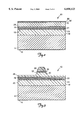
- FIG. 7A and 7B are cross-sectional views of substrates which show positive and negative sloped profiles, respectively, made in accordance with the invention.
- a manufacturable index-guided laser is required for all blue-green laser applications in which the optical quality of the beam, or the threshold current is an important issue.
- the process described here enhances the manufacturability and the reliability of these devices.
- the method of the invention is useful in fabricating blue-green laser diodes wherein a selective wet etching step is included.
- a selective wet etching step is included.
- That process included ion beam etching using Xe ions.
- the ion beam may damage the device and may lead to accelerated degradation at the edges of the laser ridge.
- the present invention is directed toward a wet etching step that removes damaged portions of the layer.
- the process uses an aqueous HX solution as an etchant where X is Cl or Br.
- this process has an advantage in that it selectively etches MgZnSSe cladding layers, and does not etch the underlying ZnSSe guiding layer of a II-VI laser diode. rhus, the etching process automatically stops at the precise depth desired for a practical index-guided. ridge laser.
- the prior art includes index-guided lasers, ion beam etching, and wet chemical etching.
- ion beam etching may lead to accelerated device degradation
- HX etches MgZnSSe may lead to accelerated device degradation
- HX etches MgZnSSe may lead to accelerated device degradation
- HX etches MgZnSSe may lead to accelerated device degradation
- HX does not etch the (100) surface of ZnSe or ZnSSe
- previously known II-VI etchants selectively etch ZnSeTe (used for contact layers) much faster than MgZnSSe, usually damaging the ZnSeTe graded contaczs, whereas HX does not
- 5) points 2, 3 and 4 can be used to efficiently fabricate blue-green laser diodes.
- HX is either HCl or HBr in an aqueous solution.
- a buried-heterostructure II-VI compound semiconductor laser diode 10 prepared in accordance with the present invention is illustraced generally in FIG. 1.
- laser diode 10 includes a ridge (typically 5 ⁇ m wide) having sides surrounded or "buried" by polycrystalline ZnS burying layer 12 to form a buried-ridge waveguide.
- the various layers of device 10 may be deposited by molecular beam epitaxy (MBE) as described in U.S. Pat. Nos. 5,291,507 and 5,363,395 which is hereby incorporated by reference.
- MBE molecular beam epitaxy
- Be can be incorporated into the layers as described in copending application Ser. No. 08/726,618, entitled BE-CONTAINING II-VI BLUE-GREEN LASER DIODES and filed on Oct. 7, 1996.
- Laser diode 10 is formed on a GaAs substrate 14 which is electrically coupled to metal contact 16.
- a lower MgZnSSe cladding layer 18 is deposited on GaAs substrate 14.
- Two ZnSSe waveguides 20 and 22 overly cladding layer 18 and are separated by a CdZnSSe quantum well 24.
- a first upper MgZnSSe cladding layer 26 overlies waveguide layer 22 and carries an etch stop layer 28.
- etch stop layer 28 comprises ZnSSe.
- any appropriate II-VI material having a reduced concentration of Mg relative to cladding layer 18 may be used.
- Etch stop layer 28 is greater thanr 50 ⁇ thick and preferably 200 ⁇ . If layer 28 is too thick, it may affect operation of laser diode 10.
- a second upper cladding layer 30 overlies etch stop layer 28 and is embedded in burying layer 12.
- ZnSeTe ohmic contact layer 32 is formed on cladding layer 30 and is covered by metal ohmic contact electrode 36.
- Metal bond pad 34 covers ohmic contact electrode 36.
- the epitaxial layers are as follows:
- ohmic contact electrode 36 comprises a 50 ⁇ layer of palladium (Pd) covered by a 1000 ⁇ layer of gold (Au) Atop the Au layer, a 10 ⁇ layer of titanium (Ti) is deposited.
- the layers are deposited in a conventional vacuum evaporator. Ti layer, although not required, is particularly useful in improving photoresist adhesion.
- a mask 38 shown in FIG. 3 is then applied atop the ohmic contact electrode.
- the size, width and positionirg of this mask is dependent upon the final configurationa of the heterostructures within the device 10.
- Hoechst Celanese photoresist and associated process AZ-5214E is applied and patterned into 4 or 5 ⁇ m lines. The lines are oriented normal to the major flat on AXTTM GaAs wafers ( ⁇ 011>) available from American Crystal Technology located in Dublin Calif.
- the device 10 is then transferred to a vacuum chamber where an ion milling etching process is implemented to form the ridge from device 10. This is used to perform an initial etch through layers 36, 32 into and 30.
- An Xe + on source is used with a beam voltage of 500 volts.
- Device 10 is rocked ⁇ 50° during ion milling and the etch rate is 0.125 ⁇ m/min.
- the beam from a He-Ne laser is directed through a window in the vacuum chamber and impinged on device 10 during the etching process.
- the ion beam removes exposed portions of layers 30, 32 and 36 which are not covered by photoresist mask 38. Portions of the laser beam reflected from device 10 are detected and monitored to determine the etch depth.
- the ion milling process is described in U.S. Pat. No. 5,404,027 which is hereby incorporated by reference.
- the etch depth is monitored with the He--Ne laser and is brought to within about 0.5 ⁇ m of layer 28. For the last 2500 ⁇ or more, the ion beam voltage is reduced to 30 volts. At approximately 2000 ⁇ before reaching the etch-stop layer 28, ion milling is stopped. The resulting structure is shown in FIG. 3 and the top of layer 30 is damaged due to the milling process.
- Device 10 is then removed from the vacuum chamber and immediately etched in an aqueous solution of HCl or HBr (concentration is determined by the amount of magnesium present in the etched layer) which selectively etches layer 30.
- etching is performed at room temperature without stirring and occurs at a rate of about 1500 ⁇ /sec using "concentrated" HCl solution.
- the ion milling step may be replaced by other known etching techniques.
- the selective chemical etch may be used to remove all of layer 30.
- Layer 30 is etched until etch-stop layer 28 is reached, at which point selective etching termninates.
- Device 10 is then removed from etchant solution rinsed and dried. This results in the structure shown in FIG. 4.
- One aspect of the invention includes the additional etch stop layer 28 spaced apart from waveguide layer 22. This design reduces the number of minority carriers which recombine at the etched surface through dark recombination (i.e., recombination which does not provide luminescence) during operation of the laser diode thereby improving device efficiency.
- a separate etch stop layer is not used and waveguide layer 22 acts as an etch stop layer. In either embodiment, waveguide layer 22 is substantially unetched by the HX.
- burying layer 12 is deposited. Referring to FIG. 5, a 1 ⁇ m layer 12 of polycrystalline ZnS is deposited. Photoresist solvent is applied causing mask layer 38 to "lift off” thereby removing layer 38 along with the portion of layer 12 which overlies laver 38. Ultrasound and acetone mays be used to cause the lift off. It may also be desired to ion etch device 10 to partially remove layer 12 and thereby expose a portion of photoresist layer 38 to facilitate lift off. However, this may not be necessary if there is sufficicut undercutting from the HX process. This lift-off process exposes layer 36 as shown in FIG. 6.
- a bond pad 34 is applied using standard techniques. For example, a 1000 ⁇ layer of Ti followed by a 2000 ⁇ layer of Au is then deposited.
- the HX will anisotropically etch the side walls of the waveguide ridge.
- the resulting profile will evolve towards either an obtuse wall angle 70 as shown in FIG. 7A or an acute wall angle 72 as shown in FIG. 7B, depending on the crystallographic orientation of the ridge 74 or 76, respectively carried on substrate 78.
- the HX etching tends to reveal a slow-etching ⁇ 111 ⁇ plane. If ridge 74 is aligned with the ⁇ 011> crystallographic direction (depending on the manufacturer, this is either parallel or perpendicular to the major flat on the wafer), undercutting results in obtuse side-wall angle 70 of about 125°.
- p-type contact 80 is larger than the active region which provides a lower series resistance for a given active area.
- the particular etch rate of the selective etch may be adjusted by controlling the concentration of Mg in the layer to be etched or by controlling the concentration of the HX solution.
- Concentrations of aqueous HX solutions useful in the invention can be in the range of 0.1N to concentrated saturated) solution.
- HCl concentrations range from 1N to 12N, more preferably from 5N to 12N, even more preferably from 10N to 12N and most preferably 12N (i.e., "concentrated HCl").
- HBr concentrations range from 1N to 8N, more preferably from 6N to 8N, and more preferably 8N (i.e., "concentrated HBr").
- Mg concentration may be determined by observing the bandgap of the material which, in one embodiment, is 2.85 eV, about 8%.
- the layer that is etched by HX is, for example, MgZnSSe, MgZnSe, BeMgZnSe, or BeMgZnSSe.
- the present invention offers advantages over the art in that it provides a useful photolithographic process and apparatus to form desired shapes in II-VI semiconductor material.
- the invention is useful with any II-VI device and is not limited to the laser diode set forth herein.
- it is useful in the fabrication of II-VI heterojunction bipolar transistors to enable contact to the base.
- the invention includes the resultant structure formed by the aforementioned etching process, including those devices which contain an etch stop layer following the fabrication process.
- any appropriate etch stop layer miay be used which etches at a rate which is less than the etch rate of the material to be removed, including a layer with a lower relative concentration of Mg.
- the etch stop should be selected such that it is compatible with the process or finished product. it will also be understood that the etch stop layer may be removed using any appropriate technique prior to completion of the fabrication process.
- II-VI semiconductor devices in accordance with the present invention are useful in electronic devices, electronic systems, optical data disk storage system, communications systems, electronic display system, laser pointers, etc.
Abstract
Description
______________________________________
LAYER           REFERENCE #  THICKNESS
______________________________________
ZnSeTe:N graded Generally 32 500     Å
contact layer
ZnSe:N contact layer
                Generally 32 0.1     μm
MgZnSSe:N cladding;
                30           0.8     μm
ZnSSe:N etch stop
                28           200     Å
MgZnSSe:N cladding;
                26           500     Å
ZnSSe:N guiding layer;
                22           0.125   μm
CdZnSSe quantum well
                24           40      Å
ZnSSe:Cl guiding layer;
                20           0.125   μm
MgZnSSe:Cl cladding;
                18           0.8     μm
ZnSe:Cl contact layer;
                (Not shown)  0.02    μm
GaAs:Si buffer layer
                Generally 14
GaAs:Si substrate
                Generally 14
______________________________________
Claims (27)
Priority Applications (8)
| Application Number | Priority Date | Filing Date | Title |
|---|---|---|---|
| US08/929,221 US6058123A (en) | 1996-10-07 | 1997-09-09 | Selective etch for II-VI semiconductors |
| PCT/US1997/017364 WO1998015996A1 (en) | 1996-10-07 | 1997-09-26 | Selective etch for ii-vi semiconductors |
| DE69723090T DE69723090T2 (en) | 1996-10-07 | 1997-09-26 | A MAGNESIUM-CONTAINING DEVICE FROM A II-VI CONNECTING SEMICONDUCTOR AND THEIR PRODUCTION METHOD |
| KR1019997002950A KR100540611B1 (en) | 1996-10-07 | 1997-09-26 | Selective etch for ii-vi semiconductors |
| EP97910719A EP0929921B1 (en) | 1996-10-07 | 1997-09-26 | A magnesium containing ii-vi semiconductor device and its fabrication method |
| JP51757298A JP3903144B2 (en) | 1996-10-07 | 1997-09-26 | ▲ II ▼-▲ VI ▼ Selective etching of semiconductor |
| AU48020/97A AU4802097A (en) | 1996-10-07 | 1997-09-26 | Selective etch for ii-vi semiconductors |
| CN97198623A CN1232578A (en) | 1996-10-07 | 1997-09-26 | Selective etch for II-VI semiconductors |
Applications Claiming Priority (2)
| Application Number | Priority Date | Filing Date | Title |
|---|---|---|---|
| US08/726,731 US5834330A (en) | 1996-10-07 | 1996-10-07 | Selective etch method for II-VI semiconductors |
| US08/929,221 US6058123A (en) | 1996-10-07 | 1997-09-09 | Selective etch for II-VI semiconductors |
Related Parent Applications (1)
| Application Number | Title | Priority Date | Filing Date |
|---|---|---|---|
| US08/726,731 Continuation-In-Part US5834330A (en) | 1996-10-07 | 1996-10-07 | Selective etch method for II-VI semiconductors |
Publications (1)
| Publication Number | Publication Date |
|---|---|
| US6058123A true US6058123A (en) | 2000-05-02 |
Family
ID=24919775
Family Applications (2)
| Application Number | Title | Priority Date | Filing Date |
|---|---|---|---|
| US08/726,731 Expired - Lifetime US5834330A (en) | 1996-10-07 | 1996-10-07 | Selective etch method for II-VI semiconductors |
| US08/929,221 Expired - Lifetime US6058123A (en) | 1996-10-07 | 1997-09-09 | Selective etch for II-VI semiconductors |
Family Applications Before (1)
| Application Number | Title | Priority Date | Filing Date |
|---|---|---|---|
| US08/726,731 Expired - Lifetime US5834330A (en) | 1996-10-07 | 1996-10-07 | Selective etch method for II-VI semiconductors |
Country Status (2)
| Country | Link |
|---|---|
| US (2) | US5834330A (en) |
| TW (1) | TW398037B (en) |
Cited By (2)
| Publication number | Priority date | Publication date | Assignee | Title |
|---|---|---|---|---|
| US6816528B1 (en) * | 1998-12-30 | 2004-11-09 | Xerox Corporation | Method and structure for nitride based laser diode arrays on a conducting substrate |
| US20050231856A1 (en) * | 2004-04-20 | 2005-10-20 | Headway Technologies, Inc. | Xenon ion beam to improve track width definition |
Families Citing this family (3)
| Publication number | Priority date | Publication date | Assignee | Title |
|---|---|---|---|---|
| US5793913A (en) * | 1996-07-10 | 1998-08-11 | Northern Telecom Limited | Method for the hybrid integration of discrete elements on a semiconductor substrate |
| WO1999039413A2 (en) * | 1998-01-28 | 1999-08-05 | Koninklijke Philips Electronics N.V. | Ii-iv lasers having index-guided structures |
| FR2805619B1 (en) * | 2000-02-24 | 2003-01-17 | Cit Alcatel | OPTICAL COMPONENT HAVING A CHEMICALLY ENGRAVED "RIDGE" STRUCTURE GUIDE AND MANUFACTURING METHOD THEREOF |
Citations (18)
| Publication number | Priority date | Publication date | Assignee | Title |
|---|---|---|---|---|
| US5213998A (en) * | 1991-05-15 | 1993-05-25 | Minnesota Mining And Manufacturing Company | Method for making an ohmic contact for p-type group II-VI compound semiconductors |
| US5248631A (en) * | 1990-08-24 | 1993-09-28 | Minnesota Mining And Manufacturing Company | Doping of iib-via semiconductors during molecular beam epitaxy using neutral free radicals |
| US5274269A (en) * | 1991-05-15 | 1993-12-28 | Minnesota Mining And Manufacturing Company | Ohmic contact for p-type group II-IV compound semiconductors |
| US5291507A (en) * | 1991-05-15 | 1994-03-01 | Minnesota Mining And Manufacturing Company | Blue-green laser diode |
| US5319219A (en) * | 1992-05-22 | 1994-06-07 | Minnesota Mining And Manufacturing Company | Single quantum well II-VI laser diode without cladding |
| EP0619602A2 (en) * | 1993-04-07 | 1994-10-12 | Sony Corporation | Semiconductor device and method for manufacturing semiconductor device |
| US5363395A (en) * | 1992-12-28 | 1994-11-08 | North American Philips Corporation | Blue-green injection laser structure utilizing II-VI compounds |
| JPH06342960A (en) * | 1993-04-07 | 1994-12-13 | Sony Corp | Selective etching method, optoelectronic element and manufacture thereof |
| US5396103A (en) * | 1991-05-15 | 1995-03-07 | Minnesota Mining And Manufacturing Company | Graded composition ohmic contact for P-type II-VI semiconductors |
| US5395791A (en) * | 1992-05-22 | 1995-03-07 | Minnesota Mining And Manufacturing Company | Growth of II VI laser diodes with quantum wells by atomic layer epitaxy and migration enhanced epitaxy |
| JPH0766494A (en) * | 1993-08-30 | 1995-03-10 | Sony Corp | Semiconductor laser |
| US5404027A (en) * | 1991-05-15 | 1995-04-04 | Minnesota Mining & Manufacturing Compay | Buried ridge II-VI laser diode |
| US5488233A (en) * | 1993-03-11 | 1996-01-30 | Kabushiki Kaisha Toshiba | Semiconductor light-emitting device with compound semiconductor layer |
| US5513199A (en) * | 1991-05-15 | 1996-04-30 | Minnesota Mining And Manufacturing Company | Blue-green laser diode |
| US5515393A (en) * | 1992-01-29 | 1996-05-07 | Sony Corporation | Semiconductor laser with ZnMgSSe cladding layers |
| JPH08122701A (en) * | 1994-10-20 | 1996-05-17 | Moritetsukusu:Kk | Laser pointer |
| US5619520A (en) * | 1994-09-09 | 1997-04-08 | Matsushita Electric Industrial Co., Ltd. | Semiconductor laser |
| JPH09139549A (en) * | 1995-11-16 | 1997-05-27 | Hitachi Ltd | Semiconductor light emitting element |
-
1996
- 1996-10-07 US US08/726,731 patent/US5834330A/en not_active Expired - Lifetime
-
1997
- 1997-09-09 US US08/929,221 patent/US6058123A/en not_active Expired - Lifetime
- 1997-10-07 TW TW086114678A patent/TW398037B/en not_active IP Right Cessation
Patent Citations (21)
| Publication number | Priority date | Publication date | Assignee | Title |
|---|---|---|---|---|
| US5248631A (en) * | 1990-08-24 | 1993-09-28 | Minnesota Mining And Manufacturing Company | Doping of iib-via semiconductors during molecular beam epitaxy using neutral free radicals |
| US5274269A (en) * | 1991-05-15 | 1993-12-28 | Minnesota Mining And Manufacturing Company | Ohmic contact for p-type group II-IV compound semiconductors |
| US5291507A (en) * | 1991-05-15 | 1994-03-01 | Minnesota Mining And Manufacturing Company | Blue-green laser diode |
| US5513199A (en) * | 1991-05-15 | 1996-04-30 | Minnesota Mining And Manufacturing Company | Blue-green laser diode |
| US5213998A (en) * | 1991-05-15 | 1993-05-25 | Minnesota Mining And Manufacturing Company | Method for making an ohmic contact for p-type group II-VI compound semiconductors |
| US5404027A (en) * | 1991-05-15 | 1995-04-04 | Minnesota Mining & Manufacturing Compay | Buried ridge II-VI laser diode |
| US5538918A (en) * | 1991-05-15 | 1996-07-23 | Minnesota Mining And Manufacturing Company | Method of fabricating a buried-ridge II-VI laser diode |
| US5396103A (en) * | 1991-05-15 | 1995-03-07 | Minnesota Mining And Manufacturing Company | Graded composition ohmic contact for P-type II-VI semiconductors |
| US5515393A (en) * | 1992-01-29 | 1996-05-07 | Sony Corporation | Semiconductor laser with ZnMgSSe cladding layers |
| US5395791A (en) * | 1992-05-22 | 1995-03-07 | Minnesota Mining And Manufacturing Company | Growth of II VI laser diodes with quantum wells by atomic layer epitaxy and migration enhanced epitaxy |
| US5319219A (en) * | 1992-05-22 | 1994-06-07 | Minnesota Mining And Manufacturing Company | Single quantum well II-VI laser diode without cladding |
| US5363395A (en) * | 1992-12-28 | 1994-11-08 | North American Philips Corporation | Blue-green injection laser structure utilizing II-VI compounds |
| US5488233A (en) * | 1993-03-11 | 1996-01-30 | Kabushiki Kaisha Toshiba | Semiconductor light-emitting device with compound semiconductor layer |
| EP0619602A2 (en) * | 1993-04-07 | 1994-10-12 | Sony Corporation | Semiconductor device and method for manufacturing semiconductor device |
| US5423943A (en) * | 1993-04-07 | 1995-06-13 | Sony Corporation | Selective etching method, optoelectronic device and its fabricating method |
| US5420446A (en) * | 1993-04-07 | 1995-05-30 | Sony Corporation | Optoelectronic semiconductor laser device having compound semiconductor first and second layers |
| JPH06342960A (en) * | 1993-04-07 | 1994-12-13 | Sony Corp | Selective etching method, optoelectronic element and manufacture thereof |
| JPH0766494A (en) * | 1993-08-30 | 1995-03-10 | Sony Corp | Semiconductor laser |
| US5619520A (en) * | 1994-09-09 | 1997-04-08 | Matsushita Electric Industrial Co., Ltd. | Semiconductor laser |
| JPH08122701A (en) * | 1994-10-20 | 1996-05-17 | Moritetsukusu:Kk | Laser pointer |
| JPH09139549A (en) * | 1995-11-16 | 1997-05-27 | Hitachi Ltd | Semiconductor light emitting element |
Non-Patent Citations (4)
| Title |
|---|
| M. Shiraishi, et al, Defect Studies in ZnSSe and ZnMgSSe by chemical etching and transmission electron microscopy, Physica Status Solidi A, vol. 152, No. 2, Dec. 16, 1995, Germany, p. 377 383, XP002054832. * |
| M. Shiraishi, et al, Defect Studies in ZnSSe and ZnMgSSe by chemical etching and transmission electron microscopy, Physica Status Solidi A, vol. 152, No. 2, Dec. 16, 1995, Germany, p. 377-383, XP002054832. |
| M.A. Haase, et al; Low Threshold Buried Ridge II VI Laser Diodes,Applied Physics Letters, vol. 63, No. 17, Oct. 25, 1993, p. 2315 2317 XP000408794. * |
| M.A. Haase, et al; Low-Threshold Buried-Ridge II-VI Laser Diodes,Applied Physics Letters, vol. 63, No. 17, Oct. 25, 1993, p. 2315-2317 XP000408794. |
Cited By (10)
| Publication number | Priority date | Publication date | Assignee | Title |
|---|---|---|---|---|
| US6816528B1 (en) * | 1998-12-30 | 2004-11-09 | Xerox Corporation | Method and structure for nitride based laser diode arrays on a conducting substrate |
| US20050231856A1 (en) * | 2004-04-20 | 2005-10-20 | Headway Technologies, Inc. | Xenon ion beam to improve track width definition |
| US7320170B2 (en) | 2004-04-20 | 2008-01-22 | Headway Technologies, Inc. | Xenon ion beam to improve track width definition |
| US20080034576A1 (en) * | 2004-04-20 | 2008-02-14 | Headway Technologies, Inc. And Tdk Corporation | Process to manufacture magnetic tunnel junction read head |
| US20080040915A1 (en) * | 2004-04-20 | 2008-02-21 | Headway Technologies, Inc. | Xenon ion beam to improve track width definition |
| US20080040914A1 (en) * | 2004-04-20 | 2008-02-21 | Headway Technologies, Inc. And Tdk Corporation | Process to manufacture CPP GMR read head |
| US20080043378A1 (en) * | 2004-04-20 | 2008-02-21 | Headway Technologies, Inc. | Pedestals for use as part of magnetic read heads |
| US7810227B2 (en) | 2004-04-20 | 2010-10-12 | Headway Technologies, Inc. | Process to manufacture CPP GMR read head |
| US8087157B2 (en) | 2004-04-20 | 2012-01-03 | Headway Technologies, Inc. | Process to manufacture magnetic tunnel junction read head |
| US8256096B2 (en) | 2004-04-20 | 2012-09-04 | Headway Technologies, Inc. | Method of using xenon ion beams to improve track width definition |
Also Published As
| Publication number | Publication date |
|---|---|
| TW398037B (en) | 2000-07-11 |
| US5834330A (en) | 1998-11-10 |
Similar Documents
| Publication | Publication Date | Title |
|---|---|---|
| EP0450255B1 (en) | Process for forming the ridge structure of a self-aligned semiconductor laser | |
| EP1329961A2 (en) | Semiconductor light-emitting element and method of manufacturing the same | |
| EP0418953B1 (en) | Method of manufacturing a semiconductor body comprising a mesa | |
| US5374328A (en) | Method of fabricating group III-V compound | |
| US6058123A (en) | Selective etch for II-VI semiconductors | |
| EP0929921B1 (en) | A magnesium containing ii-vi semiconductor device and its fabrication method | |
| US5270245A (en) | Method of forming a light emitting diode | |
| WO1998015996A9 (en) | Selective etch for ii-vi semiconductors | |
| US6083841A (en) | Method of etching gallium-nitride based compound semiconductor layer and method of manufacturing semiconductor light emitting device utilizing the same | |
| JP3460181B2 (en) | Vertical cavity type light emitting device and method of manufacturing the same | |
| US5674779A (en) | Method for fabricating a ridge-shaped laser in a channel | |
| US5215929A (en) | Method of manufacturing pn-junction device II-VI compound semiconductor | |
| JPH08148479A (en) | Etching mask of semiconductor, manufacture thereof, semiconductor processing method, and manufacture of semiconductor laser | |
| JPS6233310B2 (en) | ||
| JPH07307528A (en) | Manufacture of blue light emitting semiconductor | |
| JPH06252501A (en) | Manufacture of semiconductor laser device | |
| JPH10242131A (en) | Method of treating surface of ii-vi compd. semiconductor and treating liq. therefor | |
| JP2567066B2 (en) | Method for manufacturing semiconductor light emitting device | |
| CA1181668A (en) | Method of preferentially etching optically flat mirror facets in ingaasp/inp heterostructures | |
| JPH07226564A (en) | Semiconductor laser device and its estimation method | |
| JPH0712099B2 (en) | Method for manufacturing semiconductor laser device | |
| JPS60213072A (en) | Manufacture of semiconductor laser device | |
| JPH0244792A (en) | Manufacture of semiconductor light emitting device | |
| JPH01223729A (en) | Manufacture of semiconductor device | |
| JPH084185B2 (en) | Method of manufacturing embedded semiconductor laser device |
Legal Events
| Date | Code | Title | Description |
|---|---|---|---|
| AS | Assignment |
Owner name: MINNESOTA MINING AND MANUFACTURING COMPANY, MINNES Free format text: ASSIGNMENT OF ASSIGNORS INTEREST;ASSIGNORS:HAASE, MICHAEL A.;BAUDE, PAUL F.;MILLER, THOMAS J.;REEL/FRAME:008713/0126 Effective date: 19970909 |
|
| AS | Assignment |
Owner name: 3M INNOVATIVE PROPERTIES COMPANY, MINNESOTA Free format text: ASSIGNMENT OF ASSIGNORS INTEREST;ASSIGNOR:MINNESOTA MINING AND MANUFACTURING COMPANY;REEL/FRAME:010504/0792 Effective date: 20000103 |
|
| STCF | Information on status: patent grant |
Free format text: PATENTED CASE |
|
| FPAY | Fee payment |
Year of fee payment: 4 |
|
| FEPP | Fee payment procedure |
Free format text: PAYOR NUMBER ASSIGNED (ORIGINAL EVENT CODE: ASPN); ENTITY STATUS OF PATENT OWNER: LARGE ENTITY |
|
| FPAY | Fee payment |
Year of fee payment: 8 |
|
| FPAY | Fee payment |
Year of fee payment: 12 |