US6059876A - Method and apparatus for growing crystals - Google Patents
Method and apparatus for growing crystals Download PDFInfo
- Publication number
- US6059876A US6059876A US09/019,500 US1950098A US6059876A US 6059876 A US6059876 A US 6059876A US 1950098 A US1950098 A US 1950098A US 6059876 A US6059876 A US 6059876A
- Authority
- US
- United States
- Prior art keywords
- melt
- vessel
- dopant
- mouth
- baffle
- Prior art date
- Legal status (The legal status is an assumption and is not a legal conclusion. Google has not performed a legal analysis and makes no representation as to the accuracy of the status listed.)
- Expired - Fee Related
Links
Images


Classifications
-
- C—CHEMISTRY; METALLURGY
- C30—CRYSTAL GROWTH
- C30B—SINGLE-CRYSTAL GROWTH; UNIDIRECTIONAL SOLIDIFICATION OF EUTECTIC MATERIAL OR UNIDIRECTIONAL DEMIXING OF EUTECTOID MATERIAL; REFINING BY ZONE-MELTING OF MATERIAL; PRODUCTION OF A HOMOGENEOUS POLYCRYSTALLINE MATERIAL WITH DEFINED STRUCTURE; SINGLE CRYSTALS OR HOMOGENEOUS POLYCRYSTALLINE MATERIAL WITH DEFINED STRUCTURE; AFTER-TREATMENT OF SINGLE CRYSTALS OR A HOMOGENEOUS POLYCRYSTALLINE MATERIAL WITH DEFINED STRUCTURE; APPARATUS THEREFOR
- C30B29/00—Single crystals or homogeneous polycrystalline material with defined structure characterised by the material or by their shape
- C30B29/02—Elements
- C30B29/06—Silicon
-
- C—CHEMISTRY; METALLURGY
- C30—CRYSTAL GROWTH
- C30B—SINGLE-CRYSTAL GROWTH; UNIDIRECTIONAL SOLIDIFICATION OF EUTECTIC MATERIAL OR UNIDIRECTIONAL DEMIXING OF EUTECTOID MATERIAL; REFINING BY ZONE-MELTING OF MATERIAL; PRODUCTION OF A HOMOGENEOUS POLYCRYSTALLINE MATERIAL WITH DEFINED STRUCTURE; SINGLE CRYSTALS OR HOMOGENEOUS POLYCRYSTALLINE MATERIAL WITH DEFINED STRUCTURE; AFTER-TREATMENT OF SINGLE CRYSTALS OR A HOMOGENEOUS POLYCRYSTALLINE MATERIAL WITH DEFINED STRUCTURE; APPARATUS THEREFOR
- C30B15/00—Single-crystal growth by pulling from a melt, e.g. Czochralski method
- C30B15/02—Single-crystal growth by pulling from a melt, e.g. Czochralski method adding crystallising materials or reactants forming it in situ to the melt
- C30B15/04—Single-crystal growth by pulling from a melt, e.g. Czochralski method adding crystallising materials or reactants forming it in situ to the melt adding doping materials, e.g. for n-p-junction
-
- Y—GENERAL TAGGING OF NEW TECHNOLOGICAL DEVELOPMENTS; GENERAL TAGGING OF CROSS-SECTIONAL TECHNOLOGIES SPANNING OVER SEVERAL SECTIONS OF THE IPC; TECHNICAL SUBJECTS COVERED BY FORMER USPC CROSS-REFERENCE ART COLLECTIONS [XRACs] AND DIGESTS
- Y10—TECHNICAL SUBJECTS COVERED BY FORMER USPC
- Y10T—TECHNICAL SUBJECTS COVERED BY FORMER US CLASSIFICATION
- Y10T117/00—Single-crystal, oriented-crystal, and epitaxy growth processes; non-coating apparatus therefor
- Y10T117/10—Apparatus
- Y10T117/1024—Apparatus for crystallization from liquid or supercritical state
- Y10T117/1032—Seed pulling
- Y10T117/1056—Seed pulling including details of precursor replenishment
Definitions
- the present invention relates to an improved method and apparatus for doping silicon and other crystals grown by the Czochralski process.
- Single crystalline semiconductor materials such as silicon are widely used in the electronics industry, particularly as a starting material for integrated circuits.
- One method of forming single crystal silicon is known as the Czochralski process.
- a seed crystal which has the desired crystal orientation, is introduced into a melt of a semiconductor such as silicon.
- the melt is contained in a quartz or graphite crucible or vessel which is heated so that the silicon melt is at or slightly above its melting point. Crystal growth is a very sensitive process. The slightest disturbance can alter the crystal and render it unsuitable for use in integrated circuits.
- the seed crystal is slowly withdrawn from the melt in an inert atmosphere such as argon as the crystal and melt are rotated such that the silicon solidifies on the seed to produce a larger cylindrical silicon crystal called a boule or ingot.
- the crucible is usually rotated in the opposite direction of the crystal rotation to assure thermal balance in the growth environment.
- the pull rate and the power are adjusted to cause the diameter of the crystal to increase in a cone shape until the desired crystal diameter is achieved.
- the withdrawal rate and heating are then adjusted to maintain the desired diameter until the crystal is terminated by increasing the power and pull rate to form a cone on the end of the crystal ingot.
- Certain impurities or dopants are commonly introduced to the melt for the purpose of modifying the electrical characteristics such as the resistance of the crystal.
- Typical dopants for silicon semiconductor crystal include arsenic, boron, antimony and red phosphorus.
- One method of adding dopants is to drop pellets of the dopant material into the molten material. However, this method is very inefficient because the vaporizing temperature of volatile dopants such as arsenic is substantially lower than the temperature of the melt and, as a result, a substantial amount of the dopant is lost through evaporation.
- Another method that has been used to dope silicon with volatile dopants such as arsenic is to suspend a quartz basket containing the dopant above the melt in an bell jar. This method is also inefficient because a large portion of the vaporized arsenic tends to flow under and out of the bell jar and does not dissolve in the silicon melt.
- the present invention provides an improved method and apparatus for doping silicon and other crystals made by the Czochralski process wherein the surface of the melt is partially enclosed or covered in order to capture the dopant vapors and improve the efficiency with which they are dissolved in the melt.
- the dopant is suspended in a vapor retention vessel such as a quartz bell jar which is suspended above the melt so that the heat from the melt causes the dopant to vaporize.
- an annular baffle is provided around the mouth of the vessel or the rim of the crucible containing the melt such that the amount of uncovered open area on the surface of the melt is reduced and the dopant vapor is retained in contact with the surface of the melt such that it dissolves more efficiently in the melt.
- the mouth of the bell jar is flared outwardly. While not desiring to be bound, flaring the mouth of the bell jar may establish an inert gas flow across the top of the melt that retains dopant where it can dissolve in the melt.
- One manifestation of the invention is a method which includes the steps of providing a crucible containing the melt; suspending a vapor-retaining vessel over the surface of the melt, the vessel having a mouth which is in close proximity to the surface of the melt; suspending a dopant within the vessel above the melt; vaporizing the dopant in the vessel; providing a baffle which extends around the mouth of the vessel or flaring outwardly the mouth of the vessel to retain the vaporized dopant in contact with the surface of the melt, and dissolving the vaporized dopant in the melt.
- the crucible is equipped with an adjustable annular shutter or iris diaphragm that can be closed around the mouth of the vapor retention vessel to retain the vaporized dopant on the surface of the melt.
- the invention also provides an apparatus for producing a silicon crystal containing a dopant comprising a vapor-retaining vessel having a mouth at its base; means for suspending a dopant in the vessel; and a baffle or flare around a mouth of the vessel to retain the vaporized dopant on the surface of the melt.
- the baffle extends outwardly from the mouth of the vessel and in another embodiment, the baffle extends inwardly from the side wall of the crucible.
- the crucible is equipped with an iris shutter or diaphragm which can be closed about the mouth of the vapor retaining vessel to close off the surface of the melt extending from the mouth of the vessel to the edge of the crucible.
- the volatile dopant is added directly to the melt in a crucible having an iris diaphragm and the diaphragm is closed to retain the dopant in contact with the surface of the melt as it vaporizes.
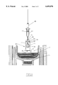
- FIG. 1 is a front view of the apparatus of the present invention showing a baffle extending from a bell jar;
- FIG. 2 is an alternate embodiment of the system of FIG. 1 wherein the baffle extends from the crucible;
- FIG. 3 is a front view of the apparatus of the invention showing a bell jar having a flared mouth in accordance with another embodiment of the invention.
- a crystal doping apparatus generally designated 10 in accordance with the present invention includes a crucible 14 containing a molten material 12, such as silicon.
- the furnace, crucible and crystal pulling apparatus have a conventional construction and are commercially available from suppliers such as Liebold, Ferrofluidics, and Kayex.
- the crucible 14 is typically provided on a platform which is generally designated 16 such that the crucible can be raised, lowered and rotated in a manner that is conventionally used in the Czochralski process.
- the doping apparatus includes a gas-retaining vessel which is preferably a quartz bell jar 18 having a closed top 22 and an open bottom 24.
- An upright quartz plate 19 including an aperture 21 is fused to the closed top end 22 of the bell jar so that the bell jar 18 can be suspended within the furnace on aperture 21 from a rod 20,
- the rod 20 can be the same rod which is used to raise and lower the seed crystal in the Czochralski process.
- the bell jar 18 is suspended over the melt 12 such that the mouth 24 faces downward and opens on the melt. Typically the mouth is about 0.75 to 1.25 inches above the surface of the melt.
- the melt is preferably 1430 degrees C. when doping silicon.
- the basket 28 is suspended from a quartz hook 29 which is carried on a quartz rod 35 fused in place inside the closed end of the jar 18.
- the basket can be suspended on a molybdenum hanger 27 which includes a sliding lock bar 34.
- the hanger 27 is made long enough to hold the basket 28 at a height in the bell jar at which the dopant will be vaporized by the heat of the melt. By adjusting the height of the basket, the rate of vaporization of the dopant can be controlled.
- the dopant is preferably suspended about 4 inches above the surface of the melt.
- a laterally-extending baffle is utilized in order to prevent the dopant vapors from traveling up the outer surface of the bell jar out of contact with the surface of the melt.
- Baffle 30 can be made from any inert and heat resistant material such as carbon, quartz or molybdenum.
- the baffle extends outwardly from the mouth 24 of the bell jar 18 as shown in FIG. 1. When the baffle is molybdenum, a cut is made in the baffle to permit thermal expansion. By covering the uncovered surface of the melt the baffle retains the dopant vapors near the surface of the melt where they can dissolve efficiently.
- the baffle that is used on a bell jar is circular in shape and extends from the periphery of the bell jar.
- the size of the baffle will vary with the type and size of furnace and pull chamber in which it is used.
- the bell jar and baffle must fit through the isolation or gate valve in the furnace and the baffle is about 30 mm to 60 mm.
- the baffle can be relatively small.
- a baffle extending as little as 6 mm from the side of the bell jar has been observed to improve dissolution of the dopant. Accordingly the baffle should be at least 6 mm wide and typically over 12 mm wide.
- baffle shown in the drawing is about 40 mm wide but substantially larger baffles may be used depending upon the type of equipment that is being used to perform the process.
- the baffle may be formed integrally with the bell jar, or in the alternative, it may be an annular ring which sits on a bead or ledge 31 around the outer rim of the mouth 24 of the bell jar.
- baffle 30 improves the efficiency with which the dopant dissolves in the melt be retaining the vapors of the dopant near the surface of the melt where they can be dissolved. If the baffle is not used, the convection currents in the furnace and on the surface of the melt carry the vaporized dopant away from the surface of the melt where it is not able to dissolve in the melt.
- a laterally-extending baffle 32 extends inwardly from the upper periphery of the crucible 14. Similar to the baffle 30 in FIG. 1, baffle 32 allows less of the dopant to escape. This baffle is also circular in shape and extends from the periphery of the crucible to the edge of the bell jar. The size of the baffle will vary with the size of the hot zone. It can either be formed integrally with the crucible or be removably-attached thereto. However, the melt should not be heated in a completely closed vessel. Hence, using the design of FIG. 2, apertures 33 can be provided in the baffle 32 located at the edge of the crucible to permit off gases to escape from the melt.
- the invention has been described with reference to the use of a vapor retention vessel such as a bell jar.
- the dopant can be added to the melt directly through a quartz doping tube in a manner that is commonly used in the art with less volatile dopants.
- the crucible is covered using an iris diaphragm. Iris diaphragms have previously been used in the Czochralski method as a means of controlling temperature wherein they are closed around the ingot or boule during the crystal growing process.
- the iris upon doping the melt (prior to introducing the seed crystal), the iris would be closed to cover the surface of the melt and thereby retain vaporized dopant in contact with the surface such that the vaporized dopant dissolves efficiently.
- the iris can be closed to a small diameter opening (e.g., 2 or 3 inches in diameter) and the dopant introduced to the melt through the center of the iris. After adding the dopant, the iris can be closed further if desired.
- a bell jar in which the mouth 50 of the bell jar is flared outwardly as shown in FIG. 3.
- the diameter of the mouth of the bell jar can be at least about 6 mm greater than the diameter of the walls of the jar above the mouth, e.g., at the vertical midpoint of the walls of the bell jar.
- an inert gas such as argon gas is introduced from the top of the furnace chamber and drawn down into the chamber by a vacuum which is pulled from the bottom of the chamber.
- Flaring the mouth of the bell jar in this way is believed to produce a gas flow in the chamber which proceeds down the side of the bell jar and is directed radially outwardly by the flared mouth across the top of the melt. This flow is believed to produce a gaseous blanket which traps the dopant vapor adjacent the surface of the melt and thereby enhances dissolution.
- a narrow baffle e.g., 6 to 20 mm
- a flared mouth can be used to improve dissolution of the dopant. While it is believed that the improvement in dissolution is attributable to the formation of a gas blanket, the applicants do not desire to be bound by this theory.
- Those skilled in the art will recognize that other bell jar configurations than that illustrated in FIG.
- the amount of flaring can vary over a wide range.
- the wall of the bell jar could be outwardly inclined instead of being vertical and the outward inclination can start at the top of the jar or at any point intermediate the top and the mouth of the jar on the wall.
- the jar need not be circular but other polygonal cross-sections could also be employed.
- the invention has been illustrated using silicon as the melt and arsenic as an example of the dopant, those skilled in the art will recognize that the invention has application wherever the Czochralski crystal growing process is used.
- the invention can also be used to dope other semiconductors such as gallium and germanium.
- the method is also useful in doping with any dopant which has a vaporization temperature which is lower than the temperature of the melt. Examples of other dopants that may be used include dopants such as red phosphorus.
Abstract
Description
Claims (28)
Priority Applications (1)
| Application Number | Priority Date | Filing Date | Title |
|---|---|---|---|
| US09/019,500 US6059876A (en) | 1997-02-06 | 1998-02-05 | Method and apparatus for growing crystals |
Applications Claiming Priority (2)
| Application Number | Priority Date | Filing Date | Title |
|---|---|---|---|
| US3929997P | 1997-02-06 | 1997-02-06 | |
| US09/019,500 US6059876A (en) | 1997-02-06 | 1998-02-05 | Method and apparatus for growing crystals |
Publications (1)
| Publication Number | Publication Date |
|---|---|
| US6059876A true US6059876A (en) | 2000-05-09 |
Family
ID=21904741
Family Applications (1)
| Application Number | Title | Priority Date | Filing Date |
|---|---|---|---|
| US09/019,500 Expired - Fee Related US6059876A (en) | 1997-02-06 | 1998-02-05 | Method and apparatus for growing crystals |
Country Status (3)
| Country | Link |
|---|---|
| US (1) | US6059876A (en) |
| AU (1) | AU6264198A (en) |
| WO (1) | WO1998035074A1 (en) |
Cited By (12)
| Publication number | Priority date | Publication date | Assignee | Title |
|---|---|---|---|---|
| JP2001342094A (en) * | 2000-05-31 | 2001-12-11 | Komatsu Electronic Metals Co Ltd | Device and method for monocrystal pulling surely executed with arsenic doping |
| US20030061985A1 (en) * | 2001-09-28 | 2003-04-03 | Memc Electronic Materials, Inc. | Process for preparing an arsenic-doped single crystal silicon using a submersed dopant feeder |
| US20040226504A1 (en) * | 2003-05-16 | 2004-11-18 | Katsunori Nakashima | Apparatus and method for supplying crystalline materials in Czochralski method |
| US20080264332A1 (en) * | 2007-04-25 | 2008-10-30 | Fareed Sepehry-Fard | Method, system, and apparatus for doping and for multi-chamber high-throughput solid-phase epitaxy deposition process |
| US20090266294A1 (en) * | 2008-04-24 | 2009-10-29 | Memc Electronic Materials, Inc. | Method and device for feeding arsenic dopant into a silicon crystal growing apparatus |
| US20100031871A1 (en) * | 2007-05-31 | 2010-02-11 | Yasuhito Narushima | Doping apparatus and method for manufacturing silicon single crystal |
| US20140033968A1 (en) * | 2012-07-31 | 2014-02-06 | MEMC Electronic Materials S.p.A | Controlled Doping Device For Single Crystal Semiconductor Material and Related Methods |
| US9102035B2 (en) | 2012-03-12 | 2015-08-11 | MEMC Electronics Materials S.p.A. | Method for machining seed rods for use in a chemical vapor deposition polysilicon reactor |
| US20150299895A1 (en) * | 2014-04-18 | 2015-10-22 | Globalwafers Co., Ltd. | Stirring apparatus of ingot casting furnace |
| US11028500B2 (en) | 2018-12-14 | 2021-06-08 | Globalwafers Co., Ltd. | Ingot puller apparatus that include a doping conduit with a porous partition member for subliming solid dopant |
| US11028499B2 (en) | 2018-12-14 | 2021-06-08 | Globalwafers Co., Ltd. | Methods for preparing a doped ingot |
| US11047065B2 (en) * | 2016-12-22 | 2021-06-29 | Sumco Corporation | Method for producing silicon single crystal, heat shield, and single crystal pulling device |
Families Citing this family (4)
| Publication number | Priority date | Publication date | Assignee | Title |
|---|---|---|---|---|
| KR20030015239A (en) * | 2000-05-10 | 2003-02-20 | 엠이엠씨 일렉트로닉 머티리얼즈 인코포레이티드 | Method and device for feeding arsenic dopant into a silicon crystal growing process |
| US6312517B1 (en) | 2000-05-11 | 2001-11-06 | Memc Electronic Materials, Inc. | Multi-stage arsenic doping process to achieve low resistivity in silicon crystal grown by czochralski method |
| KR101330408B1 (en) * | 2011-08-12 | 2013-11-15 | 주식회사 엘지실트론 | Apparatus of ingot growing and method of the same |
| CN115323489A (en) * | 2022-08-23 | 2022-11-11 | 宁夏中欣晶圆半导体科技有限公司 | Doping method and doping device for heavily doped silicon single crystal |
Citations (45)
| Publication number | Priority date | Publication date | Assignee | Title |
|---|---|---|---|---|
| US2894863A (en) * | 1955-12-15 | 1959-07-14 | Gen Electric Co Ltd | Production of semi-conductor bodies |
| US3119778A (en) * | 1959-01-20 | 1964-01-28 | Clevite Corp | Method and apparatus for crystal growth |
| US3342560A (en) * | 1963-10-28 | 1967-09-19 | Siemens Ag | Apparatus for pulling semiconductor crystals |
| US3716345A (en) * | 1969-03-18 | 1973-02-13 | Siemens Ag | Czochralski crystallization of gallium arsenide using a boron oxide sealed device |
| US3804682A (en) * | 1971-08-26 | 1974-04-16 | Siemens Ag | Method for controlled doping of semiconductor crystals |
| US3858549A (en) * | 1973-08-15 | 1975-01-07 | Siemens Ag | Apparatus for controlled doping of semiconductor crystals |
| US4200621A (en) * | 1978-07-18 | 1980-04-29 | Motorola, Inc. | Sequential purification and crystal growth |
| US4270972A (en) * | 1980-03-31 | 1981-06-02 | Rockwell International Corporation | Method for controlled doping semiconductor material with highly volatile dopant |
| US4330362A (en) * | 1978-05-17 | 1982-05-18 | Wacker-Chemitronic Gesellschaft Fur Elektronik-Grundstoffe Mbh | Device and process for pulling high-purity semiconductor rods from a melt |
| US4330361A (en) * | 1980-02-14 | 1982-05-18 | Wacker-Chemitronic Gesellschaft Fur Elektronic-Grundstoffe Mbh | Process for the manufacture of high-purity monocrystals |
| US4400232A (en) * | 1981-11-09 | 1983-08-23 | Eagle-Picher Industries, Inc. | Control of oxygen- and carbon-related crystal defects in silicon processing |
| US4406731A (en) * | 1981-06-09 | 1983-09-27 | Ferrofluidics Corporation | Apparatus for and method of sealing shafts in crystal-growing furnace systems |
| US4410494A (en) * | 1981-04-13 | 1983-10-18 | Siltec Corporation | Apparatus for controlling flow of molten material between crystal growth furnaces and a replenishment crucible |
| US4522791A (en) * | 1982-12-02 | 1985-06-11 | Texas Instruments Incorporated | Arsenic cell stabilization valve for gallium arsenide in-situ compounding |
| US4591409A (en) * | 1984-05-03 | 1986-05-27 | Texas Instruments Incorporated | Control of nitrogen and/or oxygen in silicon via nitride oxide pressure during crystal growth |
| JPS61275196A (en) * | 1985-05-29 | 1986-12-05 | Toshiba Corp | Production of gaas single crystal |
| US4650540A (en) * | 1975-07-09 | 1987-03-17 | Milton Stoll | Methods and apparatus for producing coherent or monolithic elements |
| US4704257A (en) * | 1983-08-31 | 1987-11-03 | Research Development Corporation Of Japan | Apparatus for growing single crystals of dissociative compounds |
| US4704258A (en) * | 1986-04-01 | 1987-11-03 | Grumman Aerospace Corporation | Method and apparatus for growth of single crystal material in space |
| US4824519A (en) * | 1987-10-22 | 1989-04-25 | Massachusetts Institute Of Technology | Method and apparatus for single crystal pulling downwardly from the lower surface of a floating melt |
| DE3806918A1 (en) * | 1988-03-03 | 1989-09-14 | Leybold Ag | Appliance for pulling single crystals |
| US4873062A (en) * | 1983-08-06 | 1989-10-10 | Sumitomo Electric Industries, Ltd. | Apparatus for the growth of single crystals |
| US4956153A (en) * | 1987-09-11 | 1990-09-11 | Shin-Etsu Handotai Co., Ltd. | Apparatus for Czochralski single crystal growing |
| US4957713A (en) * | 1986-11-26 | 1990-09-18 | Kravetsky Dmitry Y | Apparatus for growing shaped single crystals |
| US5004519A (en) * | 1986-12-12 | 1991-04-02 | Texas Instruments Incorporated | Radiation heat shield for silicon melt-in manufacturing of single crystal silicon |
| US5007980A (en) * | 1988-11-01 | 1991-04-16 | Sfa, Inc. | Liquid encapsulated zone melting crystal growth method and apparatus |
| US5057287A (en) * | 1988-11-01 | 1991-10-15 | Sfa, Inc. | Liquid encapsulated zone melting crystal growth method and apparatus |
| US5059401A (en) * | 1989-07-31 | 1991-10-22 | Shin-Etsu Handotai Co., Ltd. | Monocrystal growing apparatus |
| US5078975A (en) * | 1990-12-18 | 1992-01-07 | The United States Of America As Represented By The Administrator Of The National Aeronautics And Space Administration | Drop deployment system for crystal growth apparatus |
| US5089082A (en) * | 1989-11-24 | 1992-02-18 | Wacker-Chemitronic Gesellschaft Fur Elektronik-Grundstoffe Mbh | Process and apparatus for producing silicon ingots having high oxygen content by crucible-free zone pulling, silicon ingots obtainable thereby and silicon wafers produced therefrom |
| US5098674A (en) * | 1987-12-03 | 1992-03-24 | Toshiba Ceramics Co., Ltd. | Powder supply device and method for a single crystal pulling apparatus |
| US5106593A (en) * | 1989-12-22 | 1992-04-21 | Shin-Etsu Handotai Co., Ltd. | Apparatus for producing czochralski-grown single crystals |
| US5126144A (en) * | 1987-09-01 | 1992-06-30 | Lts Lohmann Therapie-Systems Gmbh & Co. Kg | Apparatus delivering nitroglycerin to the skin, process for the production thereof and use thereof |
| US5135887A (en) * | 1989-10-10 | 1992-08-04 | International Business Machines Corporation | Boron source for silicon molecular beam epitaxy |
| US5139750A (en) * | 1989-10-16 | 1992-08-18 | Nkk Corporation | Silicon single crystal manufacturing apparatus |
| US5143704A (en) * | 1989-10-26 | 1992-09-01 | Nkk Corporation | Apparatus for manufacturing silicon single crystals |
| US5205997A (en) * | 1989-07-31 | 1993-04-27 | Grumman Aerospace Corporation | Ampoule for crystal growth |
| US5223077A (en) * | 1990-04-27 | 1993-06-29 | Osaka Titanium Co., Ltd. | Method of manufacturing single-crystal silicon |
| US5242531A (en) * | 1991-03-01 | 1993-09-07 | Wacker-Chemitronic Gesellschaft Fur Elektronik-Grundstoffe M.B.H. | Continuous liquid silicon recharging process in czochralski crucible pulling |
| US5270020A (en) * | 1991-04-15 | 1993-12-14 | Nkk Corporation | Apparatus for manufacturing silicon single crystals |
| US5292487A (en) * | 1991-04-16 | 1994-03-08 | Sumitomo Electric Industries, Ltd. | Czochralski method using a member for intercepting radiation from raw material molten solution and apparatus therefor |
| US5312600A (en) * | 1990-03-20 | 1994-05-17 | Toshiba Ceramics Co. | Silicon single crystal manufacturing apparatus |
| US5316742A (en) * | 1991-06-24 | 1994-05-31 | Komatsu Electronic Metals Co., Ltd. | Single crystal pulling apparatus |
| US5370078A (en) * | 1992-12-01 | 1994-12-06 | Wisconsin Alumni Research Foundation | Method and apparatus for crystal growth with shape and segregation control |
| US5450814A (en) * | 1992-10-26 | 1995-09-19 | Research Development Corporation Of Japan | Single crystal pulling apparatus having slidable shield plate to control area of opening around single crystal |
-
1998
- 1998-02-05 US US09/019,500 patent/US6059876A/en not_active Expired - Fee Related
- 1998-02-05 WO PCT/US1998/002030 patent/WO1998035074A1/en active Application Filing
- 1998-02-05 AU AU62641/98A patent/AU6264198A/en not_active Abandoned
Patent Citations (46)
| Publication number | Priority date | Publication date | Assignee | Title |
|---|---|---|---|---|
| US2894863A (en) * | 1955-12-15 | 1959-07-14 | Gen Electric Co Ltd | Production of semi-conductor bodies |
| US3119778A (en) * | 1959-01-20 | 1964-01-28 | Clevite Corp | Method and apparatus for crystal growth |
| US3342560A (en) * | 1963-10-28 | 1967-09-19 | Siemens Ag | Apparatus for pulling semiconductor crystals |
| US3716345A (en) * | 1969-03-18 | 1973-02-13 | Siemens Ag | Czochralski crystallization of gallium arsenide using a boron oxide sealed device |
| US3804682A (en) * | 1971-08-26 | 1974-04-16 | Siemens Ag | Method for controlled doping of semiconductor crystals |
| US3858549A (en) * | 1973-08-15 | 1975-01-07 | Siemens Ag | Apparatus for controlled doping of semiconductor crystals |
| US4650540A (en) * | 1975-07-09 | 1987-03-17 | Milton Stoll | Methods and apparatus for producing coherent or monolithic elements |
| US4330362A (en) * | 1978-05-17 | 1982-05-18 | Wacker-Chemitronic Gesellschaft Fur Elektronik-Grundstoffe Mbh | Device and process for pulling high-purity semiconductor rods from a melt |
| US4200621A (en) * | 1978-07-18 | 1980-04-29 | Motorola, Inc. | Sequential purification and crystal growth |
| US4330361A (en) * | 1980-02-14 | 1982-05-18 | Wacker-Chemitronic Gesellschaft Fur Elektronic-Grundstoffe Mbh | Process for the manufacture of high-purity monocrystals |
| US4270972A (en) * | 1980-03-31 | 1981-06-02 | Rockwell International Corporation | Method for controlled doping semiconductor material with highly volatile dopant |
| US4410494A (en) * | 1981-04-13 | 1983-10-18 | Siltec Corporation | Apparatus for controlling flow of molten material between crystal growth furnaces and a replenishment crucible |
| US4406731A (en) * | 1981-06-09 | 1983-09-27 | Ferrofluidics Corporation | Apparatus for and method of sealing shafts in crystal-growing furnace systems |
| US4400232A (en) * | 1981-11-09 | 1983-08-23 | Eagle-Picher Industries, Inc. | Control of oxygen- and carbon-related crystal defects in silicon processing |
| US4522791A (en) * | 1982-12-02 | 1985-06-11 | Texas Instruments Incorporated | Arsenic cell stabilization valve for gallium arsenide in-situ compounding |
| US4873062A (en) * | 1983-08-06 | 1989-10-10 | Sumitomo Electric Industries, Ltd. | Apparatus for the growth of single crystals |
| US4704257A (en) * | 1983-08-31 | 1987-11-03 | Research Development Corporation Of Japan | Apparatus for growing single crystals of dissociative compounds |
| US4591409A (en) * | 1984-05-03 | 1986-05-27 | Texas Instruments Incorporated | Control of nitrogen and/or oxygen in silicon via nitride oxide pressure during crystal growth |
| JPS61275196A (en) * | 1985-05-29 | 1986-12-05 | Toshiba Corp | Production of gaas single crystal |
| US4704258A (en) * | 1986-04-01 | 1987-11-03 | Grumman Aerospace Corporation | Method and apparatus for growth of single crystal material in space |
| US4957713A (en) * | 1986-11-26 | 1990-09-18 | Kravetsky Dmitry Y | Apparatus for growing shaped single crystals |
| US5004519A (en) * | 1986-12-12 | 1991-04-02 | Texas Instruments Incorporated | Radiation heat shield for silicon melt-in manufacturing of single crystal silicon |
| US5126144A (en) * | 1987-09-01 | 1992-06-30 | Lts Lohmann Therapie-Systems Gmbh & Co. Kg | Apparatus delivering nitroglycerin to the skin, process for the production thereof and use thereof |
| US4956153A (en) * | 1987-09-11 | 1990-09-11 | Shin-Etsu Handotai Co., Ltd. | Apparatus for Czochralski single crystal growing |
| US4824519A (en) * | 1987-10-22 | 1989-04-25 | Massachusetts Institute Of Technology | Method and apparatus for single crystal pulling downwardly from the lower surface of a floating melt |
| US5098674A (en) * | 1987-12-03 | 1992-03-24 | Toshiba Ceramics Co., Ltd. | Powder supply device and method for a single crystal pulling apparatus |
| DE3806918A1 (en) * | 1988-03-03 | 1989-09-14 | Leybold Ag | Appliance for pulling single crystals |
| US5007980A (en) * | 1988-11-01 | 1991-04-16 | Sfa, Inc. | Liquid encapsulated zone melting crystal growth method and apparatus |
| US5057287A (en) * | 1988-11-01 | 1991-10-15 | Sfa, Inc. | Liquid encapsulated zone melting crystal growth method and apparatus |
| US5059401A (en) * | 1989-07-31 | 1991-10-22 | Shin-Etsu Handotai Co., Ltd. | Monocrystal growing apparatus |
| US5205997A (en) * | 1989-07-31 | 1993-04-27 | Grumman Aerospace Corporation | Ampoule for crystal growth |
| US5135887A (en) * | 1989-10-10 | 1992-08-04 | International Business Machines Corporation | Boron source for silicon molecular beam epitaxy |
| US5139750A (en) * | 1989-10-16 | 1992-08-18 | Nkk Corporation | Silicon single crystal manufacturing apparatus |
| US5143704A (en) * | 1989-10-26 | 1992-09-01 | Nkk Corporation | Apparatus for manufacturing silicon single crystals |
| US5089082A (en) * | 1989-11-24 | 1992-02-18 | Wacker-Chemitronic Gesellschaft Fur Elektronik-Grundstoffe Mbh | Process and apparatus for producing silicon ingots having high oxygen content by crucible-free zone pulling, silicon ingots obtainable thereby and silicon wafers produced therefrom |
| US5106593A (en) * | 1989-12-22 | 1992-04-21 | Shin-Etsu Handotai Co., Ltd. | Apparatus for producing czochralski-grown single crystals |
| US5312600A (en) * | 1990-03-20 | 1994-05-17 | Toshiba Ceramics Co. | Silicon single crystal manufacturing apparatus |
| US5223077A (en) * | 1990-04-27 | 1993-06-29 | Osaka Titanium Co., Ltd. | Method of manufacturing single-crystal silicon |
| US5078975A (en) * | 1990-12-18 | 1992-01-07 | The United States Of America As Represented By The Administrator Of The National Aeronautics And Space Administration | Drop deployment system for crystal growth apparatus |
| US5242531A (en) * | 1991-03-01 | 1993-09-07 | Wacker-Chemitronic Gesellschaft Fur Elektronik-Grundstoffe M.B.H. | Continuous liquid silicon recharging process in czochralski crucible pulling |
| US5324488A (en) * | 1991-03-01 | 1994-06-28 | Wacker-Chemitronic Gesellschaft Fur Elektronik-Grundstoff M.B.H. | Continuous liquid silicon recharging process in czochralski crucible pulling |
| US5270020A (en) * | 1991-04-15 | 1993-12-14 | Nkk Corporation | Apparatus for manufacturing silicon single crystals |
| US5292487A (en) * | 1991-04-16 | 1994-03-08 | Sumitomo Electric Industries, Ltd. | Czochralski method using a member for intercepting radiation from raw material molten solution and apparatus therefor |
| US5316742A (en) * | 1991-06-24 | 1994-05-31 | Komatsu Electronic Metals Co., Ltd. | Single crystal pulling apparatus |
| US5450814A (en) * | 1992-10-26 | 1995-09-19 | Research Development Corporation Of Japan | Single crystal pulling apparatus having slidable shield plate to control area of opening around single crystal |
| US5370078A (en) * | 1992-12-01 | 1994-12-06 | Wisconsin Alumni Research Foundation | Method and apparatus for crystal growth with shape and segregation control |
Cited By (23)
| Publication number | Priority date | Publication date | Assignee | Title |
|---|---|---|---|---|
| JP2001342094A (en) * | 2000-05-31 | 2001-12-11 | Komatsu Electronic Metals Co Ltd | Device and method for monocrystal pulling surely executed with arsenic doping |
| JP4530483B2 (en) * | 2000-05-31 | 2010-08-25 | Sumco Techxiv株式会社 | CZ method single crystal pulling equipment |
| US7132091B2 (en) * | 2001-09-28 | 2006-11-07 | Memc Electronic Materials, Inc. | Single crystal silicon ingot having a high arsenic concentration |
| WO2003027362A1 (en) * | 2001-09-28 | 2003-04-03 | Memc Electronic Materials, Inc. | Process for preparing an arsenic-doped single crystal silicon using a submersed dopant feeder |
| US20030061985A1 (en) * | 2001-09-28 | 2003-04-03 | Memc Electronic Materials, Inc. | Process for preparing an arsenic-doped single crystal silicon using a submersed dopant feeder |
| US20040226504A1 (en) * | 2003-05-16 | 2004-11-18 | Katsunori Nakashima | Apparatus and method for supplying crystalline materials in Czochralski method |
| US7001456B2 (en) * | 2003-05-16 | 2006-02-21 | Sumitomo Mitsubishi Silicon Corporation | Apparatus and method for supplying Crystalline materials in czochralski method |
| US20080264332A1 (en) * | 2007-04-25 | 2008-10-30 | Fareed Sepehry-Fard | Method, system, and apparatus for doping and for multi-chamber high-throughput solid-phase epitaxy deposition process |
| US20140190401A1 (en) * | 2007-04-25 | 2014-07-10 | Fareed Sepehry-Fard | Method, system, and apparatus for doping and for multi-chamber high-throughput solid-phase epitaxy deposition process |
| DE112008000074B4 (en) * | 2007-05-31 | 2018-02-01 | Sumco Techxiv Corp. | Doping device and method for producing a silicon single crystal |
| US20100031871A1 (en) * | 2007-05-31 | 2010-02-11 | Yasuhito Narushima | Doping apparatus and method for manufacturing silicon single crystal |
| US8715416B2 (en) * | 2007-05-31 | 2014-05-06 | Sumco Techxiv Corporation | Doping apparatus for simultaneously injecting two dopants into a semiconductor melt at different positions and method for manufacturing silicon single crystal using the doping apparatus |
| US8696811B2 (en) | 2008-04-24 | 2014-04-15 | Memc Electronic Materials, Inc. | Method for feeding arsenic dopant into a silicon crystal growing apparatus |
| US7922817B2 (en) | 2008-04-24 | 2011-04-12 | Memc Electronic Materials, Inc. | Method and device for feeding arsenic dopant into a silicon crystal growing apparatus |
| US20100132829A1 (en) * | 2008-04-24 | 2010-06-03 | Memc Electronic Materials, Inc. | Method for feeding arsenic dopant into a silicon crystal growing apparatus |
| US20090266294A1 (en) * | 2008-04-24 | 2009-10-29 | Memc Electronic Materials, Inc. | Method and device for feeding arsenic dopant into a silicon crystal growing apparatus |
| US9102035B2 (en) | 2012-03-12 | 2015-08-11 | MEMC Electronics Materials S.p.A. | Method for machining seed rods for use in a chemical vapor deposition polysilicon reactor |
| US20140033968A1 (en) * | 2012-07-31 | 2014-02-06 | MEMC Electronic Materials S.p.A | Controlled Doping Device For Single Crystal Semiconductor Material and Related Methods |
| US20150299895A1 (en) * | 2014-04-18 | 2015-10-22 | Globalwafers Co., Ltd. | Stirring apparatus of ingot casting furnace |
| US9708727B2 (en) * | 2014-04-18 | 2017-07-18 | Globalwafers Co., Ltd. | Stirring apparatus of ingot casting furnace |
| US11047065B2 (en) * | 2016-12-22 | 2021-06-29 | Sumco Corporation | Method for producing silicon single crystal, heat shield, and single crystal pulling device |
| US11028500B2 (en) | 2018-12-14 | 2021-06-08 | Globalwafers Co., Ltd. | Ingot puller apparatus that include a doping conduit with a porous partition member for subliming solid dopant |
| US11028499B2 (en) | 2018-12-14 | 2021-06-08 | Globalwafers Co., Ltd. | Methods for preparing a doped ingot |
Also Published As
| Publication number | Publication date |
|---|---|
| AU6264198A (en) | 1998-08-26 |
| WO1998035074A1 (en) | 1998-08-13 |
Similar Documents
| Publication | Publication Date | Title |
|---|---|---|
| US6059876A (en) | Method and apparatus for growing crystals | |
| US5904768A (en) | Process for controlling the oxygen content in silicon wafers heavily doped with antimony or arsenic | |
| US5891245A (en) | Single crystal pulling method and apparatus for its implementation | |
| US3511610A (en) | Silicon crystal growing | |
| US5788718A (en) | Apparatus and a method for growing a single crystal | |
| JP2813592B2 (en) | Single crystal manufacturing method | |
| JPH08295591A (en) | Doping device | |
| EP0417948A2 (en) | Method and apparatus for pulling up silicon single crystal | |
| KR102138455B1 (en) | A heat shield member for single crystal growth and single crystal growth apparatus using the same | |
| KR100462137B1 (en) | Single crystal pulling apparatus | |
| JPH0412087A (en) | Apparatus for producing silicon single crystal | |
| JPH03247585A (en) | Crystal growing method | |
| TWI806139B (en) | Single crystal manufacturing apparatus | |
| JP2001010890A (en) | Single crystal pulling device | |
| JPH04198086A (en) | Process for growing single crystal | |
| JPH04305091A (en) | Method and device for pulling up single crystal | |
| EP0221051A1 (en) | Method and apparatus for growing single crystal bodies | |
| JPH01160891A (en) | Apparatus for pulling up single crystal | |
| JPH07330482A (en) | Method and apparatus for growing single crystal | |
| JP3885245B2 (en) | Single crystal pulling method | |
| JP2825938B2 (en) | Single crystal pulling device | |
| JP3470479B2 (en) | Single crystal pulling device | |
| JPH05301793A (en) | Apparatus for drawing single crystal | |
| JPH05238883A (en) | Production of single crystal silicone rod and apparatus for production | |
| JPH04321590A (en) | Growing method of single crystal |
Legal Events
| Date | Code | Title | Description |
|---|---|---|---|
| AS | Assignment |
Owner name: CRYSTECO, INC., OHIO Free format text: ASSIGNMENT OF ASSIGNORS INTEREST;ASSIGNORS:YIN, PHILIP C.S.;BLOSSER, PHILIP EDWARD;JONES, RODGER F.;REEL/FRAME:009309/0327 Effective date: 19980206 |
|
| AS | Assignment |
Owner name: ROBINSON, WILLIAM H., OHIO Free format text: ASSIGNMENT OF ASSIGNORS INTEREST;ASSIGNOR:CRYSTEO, INC.;REEL/FRAME:010571/0318 Effective date: 20000110 |
|
| AS | Assignment |
Owner name: ROBINSON, WILLIAM H., OHIO Free format text: RE-RECORD TO CORRECT THE ASSIGNOR'S NAME, PREVIOUSLY RECORDED ON REEL 010571 FRAME 0318, AQSSIGNOR CONFIRMS THE ASSIGNMENT OF THE ENTIRE INTEREST.;ASSIGNOR:CRYSTECO, INC.;REEL/FRAME:011161/0348 Effective date: 20000110 |
|
| REMI | Maintenance fee reminder mailed | ||
| LAPS | Lapse for failure to pay maintenance fees | ||
| FP | Lapsed due to failure to pay maintenance fee |
Effective date: 20040509 |
|
| STCH | Information on status: patent discontinuation |
Free format text: PATENT EXPIRED DUE TO NONPAYMENT OF MAINTENANCE FEES UNDER 37 CFR 1.362 |