US6075730A - High performance cost optimized memory with delayed memory writes - Google Patents
High performance cost optimized memory with delayed memory writes Download PDFInfo
- Publication number
- US6075730A US6075730A US09/169,729 US16972998A US6075730A US 6075730 A US6075730 A US 6075730A US 16972998 A US16972998 A US 16972998A US 6075730 A US6075730 A US 6075730A
- Authority
- US
- United States
- Prior art keywords
- memory
- write
- data
- read
- control
- Prior art date
- Legal status (The legal status is an assumption and is not a legal conclusion. Google has not performed a legal analysis and makes no representation as to the accuracy of the status listed.)
- Expired - Lifetime
Links
Images


Classifications
-
- G—PHYSICS
- G11—INFORMATION STORAGE
- G11C—STATIC STORES
- G11C7/00—Arrangements for writing information into, or reading information out from, a digital store
- G11C7/22—Read-write [R-W] timing or clocking circuits; Read-write [R-W] control signal generators or management
-
- G—PHYSICS
- G11—INFORMATION STORAGE
- G11C—STATIC STORES
- G11C7/00—Arrangements for writing information into, or reading information out from, a digital store
- G11C7/10—Input/output [I/O] data interface arrangements, e.g. I/O data control circuits, I/O data buffers
- G11C7/1072—Input/output [I/O] data interface arrangements, e.g. I/O data control circuits, I/O data buffers for memories with random access ports synchronised on clock signal pulse trains, e.g. synchronous memories, self timed memories
-
- G—PHYSICS
- G11—INFORMATION STORAGE
- G11C—STATIC STORES
- G11C2207/00—Indexing scheme relating to arrangements for writing information into, or reading information out from, a digital store
- G11C2207/22—Control and timing of internal memory operations
- G11C2207/229—Timing of a write operation
Definitions
- the present invention relates generally to electronic systems for data storage and retrieval. More particularly, the invention is directed toward improved methods and structures for memory devices.
- the present invention introduces novel methods and structures for reducing the cost of memory devices while minimally compromising their performance.
- the description of the invention requires a significant amount of background including: application requirements, memory device physical construction, and memory device logical operation.
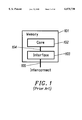
- FIG. 1 shows the general organization of a memory device.
- Memory device 101 consists of a core 102 and an interface 103.
- the core is responsible for storage of the information.
- the interface is responsible for translating the external signalling used by the interconnect 105 to the internal signaling carried on bus 104.
- the primitive operations of the core include at least a read operation.
- a conventional dynamic random access memory (DRAM) has at least write, precharge, and sense operations in addition to the read operation.
- DRAM dynamic random access memory
- FIG. 2 is a block diagram of a conventional DRAM core 102. Since the structure and operation of a conventional DRAM core is well known in the art only a brief overview is presented here.
- a conventional DRAM core 202 mainly comprises storage banks 211 and 221, row decoder and control circuitry 210, and column data path circuit comprising column amplifiers 260 and column decoder and control circuitry 230.
- Each of the storage banks comprises storage arrays 213 and 223 and sense amplifiers 212 and 222.
- the row and column decoders may be replicated in order to form the logical decoder shown in FIG. 2.
- the column i/o lines 245 may be either bidirectional, as shown, or unidirectional, in which case separate column i/o lines are provided for read and write operations.
- Row operations control the storage array word lines 241 and the sense amplifiers via line 242. These operations control the movement of data from the selected row of the selected storage array to the selected sense amplifier via the bit lines 251 and 252.
- Column operations control the movement of data from the selected sense amplifiers to and from the external data connections 204d and 204e.
- Device selection is generally accomplished by one of the following choices:
- FIG. 3 illustrates the timing required to perform the row operations of precharge and sense. In their abstract form these operations can be defined as
- PRECH and PRECHBANK form signals on line 204a in which PRECHBANK presents the "bank” argument of the precharge operation
- SENSE, SENSEBANK and SENSEROW form signals on line 204b in which SENSEBANK and SENSEROW present the "bank” and "row” arguments, respectively, for the sense operation.
- t RP , t RAS ,min, and t RCD can have significant variations between devices using the same design and across different designs using the same architecture.
- FIG. 5 and FIG. 6 illustrate the timing requirements of the read and write operations, respectively. These operations can be defined abstractly as:
- More recent conventional DRAM cores allow a certain amount of concurrent operation between the functional blocks of the core. For example, it is possible to independently operate the precharge and sense operations or to operate the column path simultaneously with row operations. To take advantage of this concurrency each of the following groups may operate somewhat independently:
- COLCYC 204f on line, COLLAT and COLADDR on lines 204g, WRITE and WMASK one lines 204c, READDATA on line 204d, and WRITEDATA on line 204.
- FIG. 7 shows the permissible sequence of operations for a single bank of a conventional DRAM core. It shows the precharge 720, sense 721, read 722, and write 723, operations as nodes in a graph. Each directed arc between operations indicates an operation which may follow. For example, arc 701 indicates that a precharge operation may follow a read operation.
- This universal sequence allows any sequence of operations needed by an application to be performed in one pass through it without repeating any step in that sequence.
- a control mechanism that implements the universal sequence can be said to be conflict free.
- a conflict free control mechanism permits a new application reference to be started for every minimum data transfer. That is, the control mechanism itself will never introduce a resource restriction that stalls the memory requester. There may be other reasons to stall the memory requester, for example references to different rows of the same bank may introduce bank contention, but lack of control resources will not be a reason for stalling the memory requester
- Memory applications may be categorized as follows:
- main memory--references generated by a processor typically with several levels of caches;
- main memory traffic can be cached or uncached processor references. Such traffic is latency sensitive since typically a processor will stall when it gets a cache miss or for any other reason needs data fetched from main memory. Addressing granularity requirements are set by the transfer size of the processor cache which connects to main memory. A typical value for the cache transfer size is 32 bytes. Since multiple memory interfaces may run in parallel it is desirable that the memory system perform well for transfer sizes smaller than this. Main memory traffic is generally not masked; that is, the vast bulk of its references are cache replacements which need not be written at any finer granularity than the cache transfer size.
- Another type of reference stream is for graphics memory. Graphics memory traffic tends to be bandwidth sensitive rather than latency sensitive. This is true because the two basic graphics engines, rendering and display refresh, can both be highly pipelined. Latency is still important since longer latency requires larger buffers in the controller and causes other second order problems. The ability to address small quanta of information is important since typical graphics data structures are manipulated according to the size of the triangle being rendered, which can be quite small. If small quanta cannot be accessed then bandwidth will be wasted transferring information which is not actually used. Traditional graphics rendering algorithms benefit substantially from the ability to mask write data; that is, to merge data sent to the memory with data already in the memory. Typically this is done at the byte level, although finer level, e.g. bit level, masking can sometimes be advantageous.
- unified applications combine the characteristics of main memory and graphics memory traffic. As electronic systems achieve higher and higher levels of integration the ability to handle these combined reference streams becomes more and more important.
- FIG. 9 shows the die of a memory device 1601 inside of a package 1620.
- the bond pads such as 1610
- the bond pads have center to center spacing significantly less than the pins of the device, such as 1640. This requires that there be some fan-in from the external pins to the internal bonding pads.
- the length of the package wiring such as 1630, grows. Observe that 1630 and 1640 are alternately used to designate package wiring.
- the overall size of the package must increase, which costs more to produce and requires more area and volume when the package is installed in the next level of the packaging hierarchy, such as on a printed circuit board.
- the stub created by the longer package wiring can affect the speed of the interconnect.
- mismatch in package wiring lengths due to the fan-in angle can affect the speed of the interconnect due to mismatched parasitics.
- the total number of signal pins has effects throughout the packaging hierarchy. For example, the memory device package requires more material, the next level of interconnect, such as a printed circuit board, requires more area, if connectors are used they will be more expensive, and the package and die area of the master device will grow.
- the memory device illustrated in FIG. 10 uses techniques typical of present day memory devices.
- a single shared command bus 1710 in conjunction with the single address bus 1720 and mask bus 1730 is used to specify all of the primitive operations comprising precharge, sense, read, and write in addition to any other overhead operations such as power management.
- FIG. 11 illustrates the operation of the memory device of FIG. 10.
- the illustrated reference sequence when classified according to Table 2 and the universal sequence previously described comprises:
- each box represents the amount of time required to transfer one bit of information across a pin of the device.
- FIG. 11 can be used to illustrate a number of techniques for specifying data transfers.
- One prior art technique uses an internal register to specify the number of data packets transferred for each read or write operation. When this register is set to its minimum value and the reference is anything besides a hit then the device has insufficient control bandwidth to specify all the required operations while simultaneously keeping the data pins highly utilized. This is shown in FIG. 11 by the gaps between data transfers. For example there is a gap between data a, 1881 and data b, 1882. Even if sufficient control bandwidth were provided some prior art devices would also require modifications to their memory cores in order to support high data pin utilization.
- Read operations do not require masking information. This leaves the mask pins 1830 available for other functions. Alternately, the mask pins during read operations may specify which bytes should actually be driven across the pins as illustrated by box 1873.
- Another technique is an alternative method of specifying that a precharge should occur by linking it to a read or write operation. When this is done the address components of the precharge operation need not be respecified; instead, a single bit can be used to specify that the precharge should occur.
- One prior art method of coding this bit is to share an address bit not otherwise needed during a read or write operation. This is illustrated by the "A-Prech" boxes, 1861 and 1862.
- FIG. 12 shows a sequence of four read references each comprising all the steps of the universal sequence.
- Table 2 do not require the multiple precharge steps of the universal sequence it is useful to examine how well a device handles the universal sequence in order to understand its ability to support mixed empty and miss nominal transactions, as well as the transitional transactions of Table 3.
- the data pins are poorly utilized. This indicates that control contention will limit the ability of the device to transfer data for various mixes of application references. The utilization of the data pins could be improved by making the burst length longer.
- the applications such as graphics applications, require small length transfers rather than large ones.
- Another technique makes the delay from write control information to data transfer different from the delay of read control information to data transfer. When writes and reads are mixed, this leads to difficulties in fully utilizing the data pins.
- current memory devices have inadequate control bandwidth for many application reference sequences.
- Current memory devices are unable to handle minimum size transfers.
- current memory devices utilize the available control bandwidth in ways that do not support efficient applications.
- Current memory devices do not schedule the use of the data pins in an efficient manner.
- current memory devices inefficiently assign a bonding pad for every pin of the device.
- a memory device includes an interconnect with control pins and bidirectional data pins.
- a memory core stores data.
- a memory interface circuit is connected to the interconnect and the memory core.
- the memory interface circuit includes a delay circuit to establish a write delay during a memory core write transaction such that the memory core write transaction has a processing time that is substantially equivalent to a memory core read transaction.
- the delay circuit delays the memory core write transaction for a time corresponding to the time required for signals to travel on the interconnect.
- FIG. 1 illustrates a known memory structure architecture
- FIG. 2 illustrates a known DRAM core structure.
- FIG. 3 illustrates Row Access Timing to a single bank in accordance with the prior art.
- FIG. 4 illustrates Row Access Timing to different banks in accordance with the prior art.
- FIG. 5 illustrates Column Read Timing in accordance with the prior art.
- FIG. 6 illustrates Column Write Timing in accordance with the prior art.
- FIG. 7 illustrates operation sequences for a conventional core DRAM.
- FIG. 8 illustrates initial and final bank states associated with a memory operation in accordance with the prior art.
- FIG. 9 illustrates a semiconductor packaging structure utilized in accordance with the prior art.
- FIG. 10 illustrates DRAM interface signals in accordance with the prior art.
- FIG. 11 illustrates a command control sequence in accordance with the prior art.
- FIG. 12 illustrates a unified control universal read sequence in accordance with an embodiment of the invention.
- FIG. 13 illustrates a unified control universal read sequence with mask precharge in accordance with an embodiment of the invention.
- FIG. 14 illustrates a unified control universal write sequence with mask precharge in accordance with an embodiment of the invention.
- FIG. 15 illustrates a unified control universal read write sequence with mask precharge in accordance with an embodiment of the invention.
- FIG. 16 illustrates a column access block diagram with no delayed write in accordance with an embodiment of the invention.
- FIG. 17 illustrates timing operations associated with a write command of an embodiment of the invention.
- FIG. 18 illustrates timing operations associated with a read command of an embodiment of the invention.
- FIG. 19 illustrates mixed read and write timing in accordance with an embodiment of the invention.
- FIG. 20 illustrates a column access with a delayed write in accordance with an embodiment of the invention.
- FIG. 21 illustrates mixed read and write timing in accordance with an embodiment of the invention.
- FIG. 22 illustrates a unified control universal read and write sequence with mask precharge and delayed write in accordance with the invention.
- FIG. 23 illustrates a split control universal read write sequence with mask precharge and delayed write in accordance with an embodiment of the invention.
- FIG. 24 illustrates a cost optimized highly concurrent memory in accordance with the invention.
- FIG. 25 illustrates a control packet format for encoding the sense operation on the primary control lines in accordance with an embodiment of the invention.
- FIG. 26 illustrates a control packet format for encoding the precharge operation on the primary control lines in accordance with an embodiment of the invention.
- FIG. 27 illustrates a packet format when masking is not used on the secondary control lines of the invention.
- FIG. 28 illustrates a packet format when masking is used on the secondary control lines of the invention.
- FIG. 29 illustrates a data block timing diagram for data packets transmitted on data wires of the invention.
- FIG. 30 illustrates a read hit in accordance with an embodiment of the invention.
- FIG. 31 illustrates an empty read in accordance with an embodiment of the invention.
- FIG. 32 illustrates a read miss in accordance with an embodiment of the invention.
- FIG. 33 illustrates a write hit in accordance with an embodiment of the invention.
- FIG. 34 illustrates an empty write in accordance with an embodiment of the invention.
- FIG. 35 illustrates a write miss in accordance with an embodiment of the invention.
- FIG. 36 illustrates reads in accordance with an embodiment of the invention.
- FIG. 37 illustrates empty byte masked writes in accordance with an embodiment of the invention.
- FIG. 38 illustrates byte masked write hits in accordance with an embodiment of the invention.
- FIG. 39 illustrates byte masked write misses in accordance with an embodiment of the invention.
- FIG. 40 illustrates reads or unmasked writes in accordance with an embodiment of the invention.
- FIG. 41 illustrates universal byte masked writes in accordance with an embodiment of the invention.
- FIG. 42 illustrates reads or unmaksed writes in accordance with an embodiment of the invention.
- FIG. 43 illustrates reads or masked writes or unmasked writes in accordance with an embodiment of the invention.
- FIG. 44 illustrates reads and unmasked writes in accordance with an embodiment of the invention.
- FIG. 45 illustrates transfers using a primary control packet for sense and precharge in accordance with an embodiment of the invention.
- FIG. 46 illustrates a memory block constructed in accordance with an embodiment of the invention.
- FIG. 47 illustrates DRAM refresh operations utilized in connection with an embodiment of the invention.
- FIG. 48 illustrates isolation pins without accompanying pads in accordance with an embodiment of the invention.
- FIG. 49 illustrates the transport of auxiliary information in accordance with an embodiment of the invention.
- FIG. 50 illustrates framing of the CMD for processing by the auxiliary transport unit in accordance with an embodiment of the invention.
- FIG. 13 shows a timing diagram according to an embodiment of the present invention in which the Mask pins 2030 carry a precharge specification rather than either the write mask information or the tristate control information, as shown in connection with FIG. 12.
- This use of the Mask pins need not be exclusive. There are multiple ways in which to indicate how the information presented on the Mask pins is to be used. For example:
- a register within the device specifies whether the mask pins are to be used for masking, tristate control, or precharge control;
- the encoding of the command pins is extended to specify, on a per operation basis, how the mask pins are to be used;
- a register bit indicates whether tristate control is enabled or not and, in the case it is not enabled, an encoding of the command pins indicates if a write is masked or not; in this embodiment all reads and unmasked writes may use the Mask pins to specify a precharge operation while masked writes do not have this capability since the Mask pins are used for mask information
- one pin indicates whether an operation should occur and the other pin indicates which bank to precharge.
- more banks are addressed by using the same pins for more than one cycle to extend the size of the bank address field.
- the device is specified in some other operation.
- the precharge specified by the mask pins shares device selection with a chip select pin that also conditions the main command pins.
- additional control bandwidth is added to the device.
- an additional chip select pin is added for sole use by the recoded mask pin precharge.
- the device address is coded on the additional bits, the device address being compared to an internal device address register.
- FIG. 13 it can be seen that the data pins are better utilized.
- the offset between data block 1982 and 1983 in FIG. 12 is reduced from 4 units of time to the 2 units of time between data blocks 2082 and 2083 of FIG. 13. This is accomplished because the precharge specification has been moved from the primary command pins 2010, to the mask pins 2030 so there is more time available on the command pins to specify the sense and read or write operations.
- FIG. 14 shows the timing of the universal write sequence in an embodiment according to the present invention, when the Mask pins are used for the precharge step.
- the offset from data block 2182 to data block 2183 is two units of time just as in the read sequence shown in FIG. 13. However, the offset from the use of the command pins to the use of the data pins is shown as zero for the write case but three for the read case.
- FIG. 15 when these sequences are combined to produce a sequence that has both reads and writes, there is a substantial gap between the write data and the read data as can be seen by the delay between data 2282 and data 2283. Delaying the write data so that the offset from control information to data is the same, independent of whether the transfer is a read or a write, reduces or eliminates the delay.
- FIG. 16 shows the column access path of a memory device in an embodiment of the invention that does not delay write data with respect to read data.
- the delay from external control 2304 to internal column control 2306 is identical whether the access is a read or a write.
- a read uses resources in the order: (a) control interconnect 2304, (b) column i/o 2307, (c) data interconnect 2305.
- a write uses them in the order: (a) control interconnect 2304, (b) data interconnect 2305, (c) column i/o 2307.
- the resource ordering of writes generally leads to the resource timing shown in FIG. 17.
- a write uses resource as shown by block 2440, the data resource as shown by block 2420, and the column resource as shown by the block 2460. This resource timing minimizes the control logic and the latency of writing data into the memory core.
- the read resource timing of FIG. 18, illustrates a minimum latency read via block 2540, column i/o block 2560, and data block 2550.
- a data bubble is introduced between blocks 2652 and 2653 of FIG. 19. This data bubble constitutes time during which the data pins are not being utilized to transfer data; the pins are inactive. Forcing the data pins to do nothing as a result of mixing reads and writes is a problem.
- the data bubble appears regardless of whether the write 2642 and the read 2643 are directed to the same or different memory devices on the channel. Further note that the delay from the control resource to the column i/o resource is identical for reads and writes. In view of this, it is impossible for the data resource timing to be identical for reads and writes.
- the optimal delay for a write does not quite match the delay for a read. Instead, it should be the minimum read delay minus the minimum turnaround time. Since the turnaround delay grows as the read delay grows, there is no need to change the write control to data delay as a function of the memory device position on the channel.
- FIG. 20 shows an embodiment of the invention having delayed write circuitry.
- the column access control information on line 2706 is delayed for writes relative to when the column control information is presented to the core for reads.
- FIG. 20 shows multiplexor 2712 which selects between the write delay block 2709 and the normal column control output of the interface.
- the interface controls the multiplexor depending upon whether the transfer is a read or a write.
- a state machine could introduce new delaying state transitions when the transfer is a write.
- FIG. 21 shows the operation of delaying the write to match the read in accordance with the present invention.
- the delay from write control block 2842 to write data block 2852 is set to match the delay from read control 2843 block to read data 2853 block less the channel turnaround time.
- the data bubble is reduced to the minimum required by channel turnaround requirements and is no longer a function of control or data resource conflicts.
- Delayed writes help optimize data bandwidth efficiency over a set of bidirectional data pins.
- One method adds delay between the control and write data packets so that the delay between them is the same or similar as that for read operations. Keeping this "pattern" the same or similar for reads and writes improves pipeline efficiency over a set of bidirectional data pins, but at the expense of added complexity in the interface.
- FIG. 22 shows that the offset between write data 2984 block and read data 2985 block has been reduced by 2 units of time, compared to the analogous situation of FIG. 15.
- FIG. 22 shows less than full utilization of the data interconnect due to the overloaded use of the command pins 2910.
- the command pins can be partitioned so that these operations are delivered to the device in an independent fashion.
- the timing of such a control method is shown in FIG. 23 where the unified control has been partitioned into fields of control information, labelled primary field 3011 and secondary field 3012.
- the primary control pins can be used to control the sense operation while the secondary control pins control read or write operations.
- Art embodiment of the present invention allows full utilization of the data pins and can transfer minimum size data blocks back-to-back, for any mix of reads or unmasked writes, for any mix of hits, misses, or empty traffic, to or from any device, any bank, any row, and any column address with only bank conflict, channel turnaround at the write-read boundaries, and 2nd order effects such as refresh limiting the data channel utilization.
- the writes could be masked or unmasked.
- FIG. 23 presumes that the memory device is designed for an interconnect structure that has zero turnaround delay between writes and reads.
- FIG. 24 shows an embodiment of the invention that has separate control interconnect resources. In one embodiment it uses delayed writes. In another embodiment it can alternately specify either a masking or a precharge field, either singly or in conjunction with another field. In another embodiment it combines delayed writes and the masking versus precharge. In an alternative embodiment according to the present invention there are three methods for starting a precharge operation in the memory core:
- Table 4 shows the specific logical pinout of the embodiment of FIG. 24 to be used for this illustrative purpose.
- FIG. 25 and FIG. 26 show two alternative control packet formats for encoding, respectively, the sense and precharge operations on the primary control lines.
- Table 5 defines the fields in the alternative formats of the primary control packet.
- the PD field selects a specific memory device.
- a combined field carries both the bank and row address arguments of the sense operation, as previously defined.
- FIG. 27 and FIG. 28 show two alternative control packet formats for encoding various operations on the secondary control lines.
- FIG. 27 shows the packet format when masking is not being performed while FIG. 28 shows the format when masking is being performed.
- Table 6 defines the fields in either format of the secondary control packet. Packet framing is accomplished via a framing, bit.
- the M field is used to indicate which format of the packet is being presented as well as indicating whether write data being written to the core should be masked.
- the SO field indicates whether a read or write operation should be performed.
- Device selection for SO specified operations is accomplished according to the SD field which is compared against an internal register that specifies the device address.
- the SA field encodes the column address of a read or write operation.
- the SB field encodes the bank address of a read or write operation. If the SPC field indicates precharge, then the precharge operation uses the SD device and SB bank address.
- the SRC field is used for power management functions.
- the MA and MB fields provide a byte masking capability when the M field indicates masking.
- the XO, XD, and XB fields provide the capability to specify a precharge operation when the M field does not indicate masking. Note that, unlike the SPC field, this specification of a precharge has a fully independent device, XD, and bank address, XB, that is not related to the read or write operations.
- FIG. 29 shows the format of the data packet transmitted on the data wires.
- FIG. 30 through FIG. 35 show a basic operation as an embodiment of the present invention, other operations can be thought of as compositions of these basic operations;
- FIG. 36 through FIG. 39 show compositions of the basic operations but distinct from notions of the universal sequence
- FIG. 40 through FIG. 43 show operations according to the universal sequence, these figures demonstrate the ability of the embodiment to handle mixed read and write with mixed hit, miss, and empty traffic without control resource conflicts;
- FIG. 44 through FIG. 45 show operations according to the universal sequence demonstrating less control conflicts than the prior art.
- Other control scheduling algorithms are possible which seek to minimize other metrics, such as service time, with or without compromising effective bandwidth.
- FIG. 30 shows a timing diagram for a nominal read hit.
- a nominal hit reference means that the beginning and final state of the addressed bank is open and that the appropriate row is already in the sense amplifiers of the addressed bank. In this case no row operation is required.
- the secondary control packet specifies the read operation, device address, bank address, and column address. Some time later, the read data is driven on the data pins. In an embodiment according to the present invention it as a constant time, later fixed by the design of the memory device.
- FIG. 31 shows a timing diagram for a nominal read empty. Recall that a nominal empty reference means that the beginning and final state of the addressed bank is closed. In order to transfer data, the addressed bank must first be sensed, then, after t RCD , the read operation takes place just as for the read hit of FIG. 30. Note that this particular example shows the precharge occurring using the primary control packet precharge mechanism. Alternately, other precharge mechanisms are used, since there are no other references contending for the control resources.
- FIG. 32 shows a timing diagram for a nominal read miss.
- a nominal miss reference means that the beginning and final state of the addressed bank is open, but that the row currently sensed in the bank is not the one addressed by the application reference.
- a precharge operation must occur, followed by a sense operation, and finally a read operation that causes the proper data to be driven out on the data pins. Any precharge mechanisms can be used.
- FIG. 33 shows a nominal write hit. Since this embodiment uses a multistep write sequence, there is a second secondary control packet in order to get the transported data sent all the way into the memory core. This second secondary control packet provides a timing reference that indicates to the memory device that it is time to send the data to the core.
- FIG. 34 shows a timing diagram for a nominal write empty.
- a write empty operation is a combination of the actions needed for a read empty and a write hit. First, a sense operation is performed, followed by a write operation, including the secondary control packet, followed by some precharge operation, although a primary precharge operation is shown.
- FIG. 35 illustrates a timing diagram for a nominal write miss.
- Write miss operation is a combination of the actions needed for a read miss and a write hit.
- a precharge operation is invoked; a primary precharge operation is shown.
- a sense operation follows, along with the two secondary control packets needed to write the data all the way to the memory core.
- FIG. 36 illustrates how one of these isolated references can be used for a sequence of memory references.
- a sequence of nominal read empty references is shown.
- the XO precharge operation is used to perform the close operation at the end of the sequence.
- the present invention thus provides another precharge mechanism that neither overloads the external control pin resources, nor adds logic to the memory device.
- FIG. 37 shows timing for a series of nominal masked write empty references.
- the XO precharge operation is not available because those control pin resources are being used to supply the mask information.
- the SPC field must be used in order to avoid bubbles, since the primary control pins are already committed to the series of sense operations. Presuming that the delay between sense and write operations is such that write read conflict problems are being avoided, as shown with the previous discussion on delayed writes, there is no real penalty for using the SPC field. This is different from reads, which would normally complete, and which desire to complete, sooner. This asymmetry between reads and writes leads to the cost reductions of the present invention by reducing required control bandwidth, while minimally impacting application performance.
- FIG. 38 shows a series of nominal masked write hit references. Note that although two secondary control packets were required to fully write data into the memory core for an isolated reference the average number needed is about one.
- FIG. 39 shows a timing diagram for a series of masked writes misses.
- the SPC field is used to precharge the bank.
- Such a sequence is useful in a graphics application which varies the length of time it keeps any bank open depending upon the amount of rendering to be done. If more than one transfer is directed to the same row of the same bank of the same device then some of the SPC precharge operations and the corresponding sense operations can be removed. This is useful both to eliminate unnecessary (precharge, sense) power but also to reduce the effective number of independent banks required to sustain the effective bandwidth, even when bank conflicts might occur.
- FIG. 40 shows a timing diagram for the universal sequence for minimum size transfers when the write traffic is not masked.
- the XO precharge operation can be consistently used for the precharge operation which begins the universal sequence, while the SPC field is used for the close operation which ends the universal sequence.
- the processor cache miss traffic typically doesn't contain frequent masked write activity but is latency sensitive. Since it does not use the masking capability it can use the XO precharge capability.
- FIG. 41 demonstrates the extra degree of freedom permitted when the transfer size per (sense, precharge) pair is twice the minimum transfer size. In this case some of the primary control bandwidth becomes available for precharge control. In this case the universal sequence can be implemented even for masked writes.
- FIG. 42 shows a timing diagram for the universal sequence for reads and unmasked writes when the transfer size is twice the minimum per (precharge, sense) pair.
- the precharge step of the universal sequence is scheduled with the primary packet precharge while the close step is scheduled with the XO precharge.
- the close step is scheduled with the XO precharge.
- not only is there adequate control bandwidth but there is more scheduling freedom for each of the steps of the universal sequence compared to the minimum transfer size per (precharge, sense) pair case.
- FIG. 43 shows a timing diagram for universal reads or masked writes or unmasked writes.
- the precharge step of the universal sequence is still scheduled in the primary control packet but the close step must be scheduled with the XO precharge operation. This reduces the scheduling flexibility compared to the unmasked case 24 but still permits full data pin utilization.
- FIG. 45 shows a timing diagram for another scheduling alternative when the transfer size is twice the minimum per (precharge, sense) pair and the traffic consists of all empty references. In this case both the sense and precharge can be scheduled on the primary control pins.
- FIG. 46 shows an alternative embodiment that includes all of the features of FIG. 24, but includes additional capability to initialize, read and write registers, and supply power control information to the memory device.
- the pinout of this embodiment is summarized in Table 8.
- FIG. 47 shows the operation sequence for the alternative embodiment of FIG. 46.
- the refresh specific operations support a novel method of handling core refresh. These new core operations create the requirements for the RefreshP and RefreshS operations coded in the primary control packet as shown in FIG. 46. In addition, various power control operations are added to the primary control packet.
- FIG. 48 shows an embodiment of the physical construction in which not all of the pins of the memory device are connected to the bond pads of the die.
- These non-connected pins provide signal isolation and shielding, thus avoiding the expense of additional bond pads.
- pin and internal conductor 5542 provides isolation for pin and internal conductors 5541 and 5543.
- the non-connected pins are signal returns, such as ground, which are adjacent to the connected pins.
- the memory device of FIG. 46 has Auxiliary information 5302 transported in time according to FIG. 49.
- Auxiliary information 5302 includes a field to specify an auxiliary operation, a control register address in the memory device, and data to be read or written from or to the control register.
- AuxClock is the AuxClock signal to the Auxiliary Transport Unit 5308 and is used to receive information from the auxiliary connections 5302 in FIG. 46. Since Auxiliary Transport Unit 5308 operates to reset or initialize the memory device, the unit need only operate slowly. Accordingly, information is framed by the CMD signal, which can be a portion of the auxiliary connections 5302, and received on the AuxIn signal as a serial bit stream.
- the format of the bit stream is shown in the tables below. As can be noted from Table 9 there are sixteen clock cycles during which a packet of information is received or obtained from the Auxiliary Transport Unit.
- the Aux information fields are the SOP[3:0] field and the SDEV[4:0] field for the SRQ packet.
- the SA packet has field SA[11:0]
- the SINT packet has a field of all zeros
- the SD packet has SD[15:0].
- the SRQ, SA, SINT and SD packets are received or obtained from the Auxiliary Transport unit in the order listed, unless only the SRQ packet is needed, in which case the other packets are not sent.
- the functions of each of the fields in the packets is tabulated in Table 10.
- the memory device is selected by the SDEV field and the SOP field determines the Auxiliary Operation to be performed by the Register Operation Unit 5309 in FIG. 46.
- the Auxiliary Transport Unit also supports the initialization of the memory device because the Auxiliary Transport Unit itself does not require initialization. This function is shown in FIG. 49.
- the CMD signal received by the Auxiliary Transport Unit has different framing information to indicate that an initialization packet follows. This causes all of the memory devices which are connected together on the same external connections in FIG. 46 to break apart a daisy chain connection formed from AuxIn through AuxOut to AuxIn of the next memory device in the chain as the initialization packet passes through the daisy chain.
- the first memory device in the chain receives a device identification field from the Auxiliary Transport unit into one of its control registers. This field serves to identify the device for future Auxiliary Transport Operations.
- the device field register is written again to change a bit, causing the first device in the chain to pass the Auxiliary information it receives to the next device in the chain. The sequence is repeated until all of the memory devices have their control registers properly configured and each device has an unique identification.
- the memory device of FIG. 46 receives power control information, specifying a change in the power mode of the memory device. While power control operations such as Powerdown and Nap are encoded into the precharge packets in one embodiment according to the present invention, other power control operations, such as ExitToNormal and ExitToDrowsy come in through the Auxiliary Transport Unit because the other units in FIG. 46 are not operational due to their reduced power state and because the Auxiliary Transport Unit operates relatively slowly compared to, for example, the Transfer Units, and so does not require much power while the other units are in their reduced power state. These Exit operations may be performed according to FIG. 50. FIG.
- the Auxiliary Transport Unit can recognize the ExitToNormal or ExitToDrowsy request.
- the memory device when a memory device receives a CMD signal 01 with 0 on the falling edge of AuxClock and 1 on the rising edge of AuxClock, the memory device will exit either the power down state or the nap state (Power State A in the timing diagram) and move to a new power state (Power State B in the diagram), depending on the state of the AuxIn Signal Line. If the AuxIn line is a 1, the memory device will exit to the normal state and if the AuxIn line is a 0 the memory device will exit to the drowsy state.
- the meaning of the AuxIn bits is reversed.
- the device that is targeted for the ExitToNormnal or ExitToDrowsy operation is received by the Auxiliary Transport Unit 5308 on the data input field via path 5307 of the memory device in FIG. 46.
- each memory device receives a different CMD signal, one for each device, rather than using the data input field via path 5307 to identify the device for a ExitToNormal or ExitToDrowsy operation.
Abstract
Description
              TABLE 1
______________________________________
Typical Core Timing Values
       Symbol
             Value (ns)
______________________________________
       t.sub.RP
             20
       t.sub.RAS,Min
             50
       t.sub.RCD
             20
       t.sub.PP
             20
       t.sub.SS
             20
       t.sub.PC
             10
       t.sub.DAC
             7
______________________________________
              TABLE 2
______________________________________
Nominal Transactions
Initial
Bank State
        Final Bank State
                   Transaction Type
                               Operations Performed
______________________________________
closed closed      empty       sense,
                               series of column
                               operations,
                               precharge
open   open        miss        precharge,
                               sense,
                               series of column
                               operations
                   hit         series of column
                               operations
______________________________________
              TABLE 3
______________________________________
Transitional Transactions
Initial Final
Bank State
        Bank State
                  Tranaction Type
                              Operations Performed
______________________________________
closed  open      empty       sense,
                              <series of column
                              operations>(optional)
open    closed    miss        <precharge,
                              sense,
                              series of column
                              operation>(optional),
                              precharge
                  hit         <series of column
                              operations>
                              (optional),
                              precharge
______________________________________
              TABLE 4
______________________________________
High Performance Logical Pin Description
                                   FIG. 24
Name              Count
                       Description        Reference
______________________________________
Primary[2:0]
          3       Primary request control
                                   3104
Secondary[4:0]
               5    Secondary request control
                                          3105
DQA[8:0]              Low order data byte
                                               3106
DQB[8:0]              High order data byte
______________________________________
TABLE 5 ______________________________________ Primary Control Packet Fields Field Description ______________________________________ PD4TDevice selector bit 4 True; for framing, device selection and broadcasting. PD4FDevice selector bit 4 False; for framing, device selection and broadcasting. PD[3:0] Device selector, least significant bits. AV Activate row; also indicates format of packet. PA[16:0] Address; combining bank and row. PB[5:0] Bank address POP[10:0] Opcode of the primary control packet. ______________________________________
              TABLE 6
______________________________________
Secondary Control Packet Fields
Field     Description
______________________________________
SD[4:0]   Device selector for Column Operation
SS=1            Start bit; for framing
M                  Mask bit, indicates if mask format is being used
SO[1:0]     Secondary Operation code
SPC              Precharge after possible Column Operation
SRC              Power management
SA[6:0]      Address for Column Operation
SB[5:0]      Bank for Column Operation
MA[7:0]      Byte mask for lower order bytes
MB[7:0]      Byte mask for higher order bytes
XD[4:0]      Device selctor for Extra Operation
XO[4:0]      Extra Operation code
XB[5:0]      Bank for Extra Operation
______________________________________
              TABLE 7
______________________________________
Nominal Timings
       Symbol
             Value (ns)
______________________________________
       t.sub.RP
             20
       t.sub.RAS,min
             60
       t.sub.RCD
             20
       t.sub.CAC
             20
______________________________________
              TABLE 8
______________________________________
Alternative High Performance Logical Pin Description
                                      FIG. 46
Name   Count   Type    Description    Reference
______________________________________
CTM    2       RSL     Transmit Clock 5301
CTMN                   (Clock To Master)
CFM    2       RSL     Receive Clock
CFMN                   (Clock From Master)
Pri-   3       RSL     Primary request control
                                      5305
mary[2:0]
Secon- 5       RSL     Secondary request control
                                      5305
dary[4:0]
DQA[8:0]
       9       RSL     Low order data byte
                                      5307
DQB[8:0]
       9       RSL     High order data byte
SIQ[1:0]
       2       CMOS    Bidirectional serial in/out for
                                      5302
                       device initialization, register
                                       and
                       ops, power mode control, and
                                      5304
                       device reset. Used to form the
                       SIO daisy chain.
SCK    1       CMOS    Serial clock for SIO and CMD
                                      5303
                       pins.
CMD    1       CMOS    Command unput used for
                                      5302
                       power mode control,
                       configuring SIO daisy chain,
                       and framing SIO operations.
______________________________________
              TABLE 9
______________________________________
Register Packet Formats
AuxClock  SRQ packet  SA packet
                               SINT    SD
______________________________________
0         rsrv        rsrv     0       SD15
1                  rsrv
                           rsrv
                                    0      SD14
2                  rsrv
                           rsrv
                                    0      SD13
3                  rsrv
                           rsrv
                                    0      SD12
4                  rsrv
                           SA11
                                    0      SD11
5                  rsrv
                           SA10
                                    0      SD10
6                  5OP3
                           5A9       0     5D9
7                  5OP2
                           SA8       0     5D8
8                 SOP1
                           SA7     0      5D7
9                 SOP0
                           5A6     0      SD6
10               SBC        SA5
                                   0      SD5
11               SDEV4
                          5A4      0      SD4
12               SDEV3
                          SA3      0      SD3
13               SDEV2
                          SA2      0      SD2
14               SDEV1
                          SA1      0      SD1
15               SDEV0
                          SA0      0      SD0
______________________________________
              TABLE 10
______________________________________
Field Description for Control Register Packets
Field     Description
______________________________________
rsrv      Reserved
SOP3..SOP0
          Serial opcode. Specifies command for control register
          transaction.
          0000 - SRD. Serial read of control register
          {SA11..SA0} of memory device {SDEV4..SDEV0}.
          0001 - SWR. Serial write of control register
          {SA11..SA0} of memory device {SDEV4..SDEV0}.
          0010 - SETR. Set Reset bit, all control registers
          assume their reset values.
          0011 - CLRR. Clear Reset bit, all control registers
          retain their reset values.
          0100 - SETF. Set fast (notmal) clock for the clock
          circuitry
SDEV4..SDEV0
          Serial device field.
SBC       Serial broadcast. When set, memory device ignores
          {SDEV..SDEV0} serial device field
SA11..SA0 Serial address. Selects which control register of the
          selected memory device is read or written.
SD15..SD0 Serial data. The 16 bits of data written to or read from
          the selected control register of the selected memory
          device.
______________________________________
Claims (6)
Priority Applications (1)
| Application Number | Priority Date | Filing Date | Title |
|---|---|---|---|
| US09/169,729 US6075730A (en) | 1997-10-10 | 1998-10-09 | High performance cost optimized memory with delayed memory writes |
Applications Claiming Priority (2)
| Application Number | Priority Date | Filing Date | Title |
|---|---|---|---|
| US6169497P | 1997-10-10 | 1997-10-10 | |
| US09/169,729 US6075730A (en) | 1997-10-10 | 1998-10-09 | High performance cost optimized memory with delayed memory writes |
Publications (1)
| Publication Number | Publication Date |
|---|---|
| US6075730A true US6075730A (en) | 2000-06-13 |
Family
ID=26741377
Family Applications (1)
| Application Number | Title | Priority Date | Filing Date |
|---|---|---|---|
| US09/169,729 Expired - Lifetime US6075730A (en) | 1997-10-10 | 1998-10-09 | High performance cost optimized memory with delayed memory writes |
Country Status (1)
| Country | Link |
|---|---|
| US (1) | US6075730A (en) |
Cited By (49)
| Publication number | Priority date | Publication date | Assignee | Title |
|---|---|---|---|---|
| US6256716B1 (en) * | 1998-12-10 | 2001-07-03 | Sun Microsystems, Inc. | Apparatus, system and method for reducing bus contention during consecutive read-write operations |
| US6370668B1 (en) * | 1999-07-23 | 2002-04-09 | Rambus Inc | High speed memory system capable of selectively operating in non-chip-kill and chip-kill modes |
| US6385094B1 (en) | 2000-09-29 | 2002-05-07 | Intel Corporation | Method and apparatus for achieving efficient memory subsystem write-to-read turnaround through read posting |
| US6453393B1 (en) | 2000-09-18 | 2002-09-17 | Intel Corporation | Method and apparatus for interfacing to a computer memory |
| US6542416B1 (en) * | 2001-11-02 | 2003-04-01 | Rambus Inc. | Methods and arrangements for conditionally enforcing CAS latencies in memory devices |
| US6618791B1 (en) | 2000-09-29 | 2003-09-09 | Intel Corporation | System and method for controlling power states of a memory device via detection of a chip select signal |
| US20040044870A1 (en) * | 2002-08-28 | 2004-03-04 | Micron Technology, Inc. | Multi-bank memory accesses using posted writes |
| US20040054845A1 (en) * | 2001-04-24 | 2004-03-18 | Rambus, Inc. | Method and apparatus for signaling between devices of a memory system |
| US6772352B1 (en) | 2000-09-29 | 2004-08-03 | Intel Corporation | Method and apparatus for reducing the rate of commands being issued if the rate exceeds a threshold which is based upon a temperature curve |
| US20040213052A1 (en) * | 2001-02-28 | 2004-10-28 | Ware Frederick A | Asynchronous, high-bandwidth memory component using calibrated timing elements |
| US20050160241A1 (en) * | 1997-10-10 | 2005-07-21 | Rambus Inc. | High performance cost optimized memory |
| US20060056244A1 (en) * | 2004-09-15 | 2006-03-16 | Ware Frederick A | Memory systems with variable delays for write data signals |
| US20060069894A1 (en) * | 2004-09-30 | 2006-03-30 | Hollis Paul W | De-coupled memory access system and method |
| US20070028060A1 (en) * | 2005-08-01 | 2007-02-01 | Ware Frederick A | Low power memory device |
| US20070177436A1 (en) * | 1997-10-10 | 2007-08-02 | Davis Paul G | Memory System and Method for Two Step Memory Write Operations |
| US20080025124A1 (en) * | 2006-07-31 | 2008-01-31 | Metaram, Inc. | Interface circuit system and method for performing power management operations utilizing power management signals |
| US20080025123A1 (en) * | 2006-07-31 | 2008-01-31 | Metaram, Inc. | Interface circuit system and method for autonomously performing power management operations in conjunction with a plurality of memory circuits |
| US20080025125A1 (en) * | 2006-07-31 | 2008-01-31 | Metaram, Inc. | Interface circuit system and method for performing power management operations in conjunction with only a portion of a memory circuit |
| US7379316B2 (en) | 2005-09-02 | 2008-05-27 | Metaram, Inc. | Methods and apparatus of stacking DRAMs |
| US7724589B2 (en) | 2006-07-31 | 2010-05-25 | Google Inc. | System and method for delaying a signal communicated from a system to at least one of a plurality of memory circuits |
| US8019589B2 (en) | 2006-07-31 | 2011-09-13 | Google Inc. | Memory apparatus operable to perform a power-saving operation |
| US8055833B2 (en) | 2006-10-05 | 2011-11-08 | Google Inc. | System and method for increasing capacity, performance, and flexibility of flash storage |
| US8060774B2 (en) | 2005-06-24 | 2011-11-15 | Google Inc. | Memory systems and memory modules |
| US8077535B2 (en) | 2006-07-31 | 2011-12-13 | Google Inc. | Memory refresh apparatus and method |
| US8080874B1 (en) | 2007-09-14 | 2011-12-20 | Google Inc. | Providing additional space between an integrated circuit and a circuit board for positioning a component therebetween |
| US8081474B1 (en) | 2007-12-18 | 2011-12-20 | Google Inc. | Embossed heat spreader |
| US8090897B2 (en) | 2006-07-31 | 2012-01-03 | Google Inc. | System and method for simulating an aspect of a memory circuit |
| US8089795B2 (en) | 2006-02-09 | 2012-01-03 | Google Inc. | Memory module with memory stack and interface with enhanced capabilities |
| US8111566B1 (en) | 2007-11-16 | 2012-02-07 | Google, Inc. | Optimal channel design for memory devices for providing a high-speed memory interface |
| US8130560B1 (en) | 2006-11-13 | 2012-03-06 | Google Inc. | Multi-rank partial width memory modules |
| US8169233B2 (en) | 2009-06-09 | 2012-05-01 | Google Inc. | Programming of DIMM termination resistance values |
| US8209479B2 (en) | 2007-07-18 | 2012-06-26 | Google Inc. | Memory circuit system and method |
| US8244971B2 (en) | 2006-07-31 | 2012-08-14 | Google Inc. | Memory circuit system and method |
| US8280714B2 (en) | 2006-07-31 | 2012-10-02 | Google Inc. | Memory circuit simulation system and method with refresh capabilities |
| US8320202B2 (en) | 2001-04-24 | 2012-11-27 | Rambus Inc. | Clocked memory system with termination component |
| US8327104B2 (en) | 2006-07-31 | 2012-12-04 | Google Inc. | Adjusting the timing of signals associated with a memory system |
| US8335894B1 (en) | 2008-07-25 | 2012-12-18 | Google Inc. | Configurable memory system with interface circuit |
| US8386722B1 (en) | 2008-06-23 | 2013-02-26 | Google Inc. | Stacked DIMM memory interface |
| US8397013B1 (en) | 2006-10-05 | 2013-03-12 | Google Inc. | Hybrid memory module |
| US8438328B2 (en) | 2008-02-21 | 2013-05-07 | Google Inc. | Emulation of abstracted DIMMs using abstracted DRAMs |
| US8566516B2 (en) | 2006-07-31 | 2013-10-22 | Google Inc. | Refresh management of memory modules |
| US8796830B1 (en) | 2006-09-01 | 2014-08-05 | Google Inc. | Stackable low-profile lead frame package |
| US8972673B2 (en) | 2006-07-31 | 2015-03-03 | Google Inc. | Power management of memory circuits by virtual memory simulation |
| US9171585B2 (en) | 2005-06-24 | 2015-10-27 | Google Inc. | Configurable memory circuit system and method |
| US9507739B2 (en) | 2005-06-24 | 2016-11-29 | Google Inc. | Configurable memory circuit system and method |
| US9542353B2 (en) | 2006-02-09 | 2017-01-10 | Google Inc. | System and method for reducing command scheduling constraints of memory circuits |
| US9632929B2 (en) | 2006-02-09 | 2017-04-25 | Google Inc. | Translating an address associated with a command communicated between a system and memory circuits |
| US10013371B2 (en) | 2005-06-24 | 2018-07-03 | Google Llc | Configurable memory circuit system and method |
| US11354064B2 (en) * | 2018-12-26 | 2022-06-07 | Micron Technology, Inc. | Detection of illegal commands |
Citations (6)
| Publication number | Priority date | Publication date | Assignee | Title |
|---|---|---|---|---|
| US5566108A (en) * | 1994-09-30 | 1996-10-15 | Nec Corporation | Synchronized semiconductor memory |
| US5724287A (en) * | 1995-05-25 | 1998-03-03 | Oki Electric Industry Co., Ltd. | Data input circuit of semiconductor storage device |
| US5748542A (en) * | 1996-12-13 | 1998-05-05 | Micron Technology, Inc. | Circuit and method for providing a substantially constant time delay over a range of supply voltages |
| US5751644A (en) * | 1996-11-26 | 1998-05-12 | Cypress Semiconductor Corporation | Data transition detect write control |
| US5761150A (en) * | 1995-05-24 | 1998-06-02 | Hitachi, Ltd. | Synchronous memory with pipelined write operation |
| US5886948A (en) * | 1996-12-20 | 1999-03-23 | Micron Technology, Inc. | Memory having a plurality of external clock signal inputs |
-
1998
- 1998-10-09 US US09/169,729 patent/US6075730A/en not_active Expired - Lifetime
Patent Citations (6)
| Publication number | Priority date | Publication date | Assignee | Title |
|---|---|---|---|---|
| US5566108A (en) * | 1994-09-30 | 1996-10-15 | Nec Corporation | Synchronized semiconductor memory |
| US5761150A (en) * | 1995-05-24 | 1998-06-02 | Hitachi, Ltd. | Synchronous memory with pipelined write operation |
| US5724287A (en) * | 1995-05-25 | 1998-03-03 | Oki Electric Industry Co., Ltd. | Data input circuit of semiconductor storage device |
| US5751644A (en) * | 1996-11-26 | 1998-05-12 | Cypress Semiconductor Corporation | Data transition detect write control |
| US5748542A (en) * | 1996-12-13 | 1998-05-05 | Micron Technology, Inc. | Circuit and method for providing a substantially constant time delay over a range of supply voltages |
| US5886948A (en) * | 1996-12-20 | 1999-03-23 | Micron Technology, Inc. | Memory having a plurality of external clock signal inputs |
Cited By (162)
| Publication number | Priority date | Publication date | Assignee | Title |
|---|---|---|---|---|
| US20090031093A1 (en) * | 1997-10-10 | 2009-01-29 | Davis Paul G | Memory System and Method for Two Step Memory Write Operations |
| US20080091907A1 (en) * | 1997-10-10 | 2008-04-17 | Barth Richard M | Integrated circuit memory device having delayed write timing based on read response time |
| US20050160241A1 (en) * | 1997-10-10 | 2005-07-21 | Rambus Inc. | High performance cost optimized memory |
| US20070198868A1 (en) * | 1997-10-10 | 2007-08-23 | Barth Richard M | Memory System Having Delayed Write Timing |
| US20070242532A1 (en) * | 1997-10-10 | 2007-10-18 | Barth Richard M | Integrated Circuit Memory Device Having Delayed Write Timing Based on Read Response Time |
| US8504790B2 (en) | 1997-10-10 | 2013-08-06 | Rambus Inc. | Memory component having write operation with multiple time periods |
| US7793039B2 (en) | 1997-10-10 | 2010-09-07 | Rambus Inc. | Interface for a semiconductor memory device and method for controlling the interface |
| US20070177436A1 (en) * | 1997-10-10 | 2007-08-02 | Davis Paul G | Memory System and Method for Two Step Memory Write Operations |
| US8560797B2 (en) | 1997-10-10 | 2013-10-15 | Rambus Inc. | Method and apparatus for indicating mask information |
| US7870357B2 (en) | 1997-10-10 | 2011-01-11 | Rambus Inc. | Memory system and method for two step memory write operations |
| US8205056B2 (en) | 1997-10-10 | 2012-06-19 | Rambus Inc. | Memory controller for controlling write signaling |
| US20070159912A1 (en) * | 1997-10-10 | 2007-07-12 | Barth Richard M | Integrated Circuit Memory Device with Delayed Write Command Processing |
| US20070147143A1 (en) * | 1997-10-10 | 2007-06-28 | Barth Richard M | Integrated Circuit Memory Device Having Delayed Write Capability |
| US8019958B2 (en) | 1997-10-10 | 2011-09-13 | Rambus Inc. | Memory write signaling and methods thereof |
| US8140805B2 (en) | 1997-10-10 | 2012-03-20 | Rambus Inc. | Memory component having write operation with multiple time periods |
| US6535968B2 (en) | 1998-12-10 | 2003-03-18 | Sun Microsystems, Inc. | Apparatus, system, and method for reducing bus contention during consecutive read-write operations |
| US6256716B1 (en) * | 1998-12-10 | 2001-07-03 | Sun Microsystems, Inc. | Apparatus, system and method for reducing bus contention during consecutive read-write operations |
| US6370668B1 (en) * | 1999-07-23 | 2002-04-09 | Rambus Inc | High speed memory system capable of selectively operating in non-chip-kill and chip-kill modes |
| US6839266B1 (en) | 1999-09-14 | 2005-01-04 | Rambus Inc. | Memory module with offset data lines and bit line swizzle configuration |
| US6453393B1 (en) | 2000-09-18 | 2002-09-17 | Intel Corporation | Method and apparatus for interfacing to a computer memory |
| US6772352B1 (en) | 2000-09-29 | 2004-08-03 | Intel Corporation | Method and apparatus for reducing the rate of commands being issued if the rate exceeds a threshold which is based upon a temperature curve |
| US6618791B1 (en) | 2000-09-29 | 2003-09-09 | Intel Corporation | System and method for controlling power states of a memory device via detection of a chip select signal |
| US6385094B1 (en) | 2000-09-29 | 2002-05-07 | Intel Corporation | Method and apparatus for achieving efficient memory subsystem write-to-read turnaround through read posting |
| US8295107B2 (en) | 2001-02-28 | 2012-10-23 | Rambus Inc. | Asynchronous pipelined memory access |
| US7529141B2 (en) | 2001-02-28 | 2009-05-05 | Rambus Inc. | Asynchronous, high-bandwidth memory component using calibrated timing elements |
| US20080144408A1 (en) * | 2001-02-28 | 2008-06-19 | Ware Frederick A | Asynchronous, high-bandwidth memory component using calibrated timing elements |
| US20090213670A1 (en) * | 2001-02-28 | 2009-08-27 | Ware Frederick A | Asynchronous, high-bandwidth memory component using calibrated timing elements |
| US7362626B2 (en) | 2001-02-28 | 2008-04-22 | Rambus Inc. | Asynchronous, high-bandwidth memory component using calibrated timing elements |
| US7830735B2 (en) | 2001-02-28 | 2010-11-09 | Rambus Inc. | Asynchronous, high-bandwidth memory component using calibrated timing elements |
| US6934201B2 (en) | 2001-02-28 | 2005-08-23 | Rambus Inc. | Asynchronous, high-bandwidth memory component using calibrated timing elements |
| US20040213052A1 (en) * | 2001-02-28 | 2004-10-28 | Ware Frederick A | Asynchronous, high-bandwidth memory component using calibrated timing elements |
| US20050237851A1 (en) * | 2001-02-28 | 2005-10-27 | Ware Frederick A | Asynchronous, high-bandwidth memory component using calibrated timing elements |
| US8059476B2 (en) | 2001-02-28 | 2011-11-15 | Rambus Inc. | Control component for controlling a delay interval within a memory component |
| US20060129776A1 (en) * | 2001-04-24 | 2006-06-15 | Ware Frederick A | Method, system and memory controller utilizing adjustable read data delay settings |
| US10236051B2 (en) | 2001-04-24 | 2019-03-19 | Rambus Inc. | Memory controller |
| US20040170072A1 (en) * | 2001-04-24 | 2004-09-02 | Rambus Inc. | Method and apparatus for coordinating memory operations among diversely-located memory components |
| US20040054845A1 (en) * | 2001-04-24 | 2004-03-18 | Rambus, Inc. | Method and apparatus for signaling between devices of a memory system |
| US8625371B2 (en) | 2001-04-24 | 2014-01-07 | Rambus Inc. | Memory component with terminated and unterminated signaling inputs |
| US20050169097A1 (en) * | 2001-04-24 | 2005-08-04 | Rambus Inc. | Method and apparatus for coordinating memory operations among diversely-located memory components |
| US7200055B2 (en) | 2001-04-24 | 2007-04-03 | Rambus Inc. | Memory module with termination component |
| US7177998B2 (en) | 2001-04-24 | 2007-02-13 | Rambus Inc. | Method, system and memory controller utilizing adjustable read data delay settings |
| US10706910B2 (en) | 2001-04-24 | 2020-07-07 | Rambus Inc. | Memory controller |
| US8391039B2 (en) | 2001-04-24 | 2013-03-05 | Rambus Inc. | Memory module with termination component |
| US8395951B2 (en) | 2001-04-24 | 2013-03-12 | Rambus Inc. | Memory controller |
| US8717837B2 (en) | 2001-04-24 | 2014-05-06 | Rambus Inc. | Memory module |
| US8760944B2 (en) | 2001-04-24 | 2014-06-24 | Rambus Inc. | Memory component that samples command/address signals in response to both edges of a clock signal |
| US20060007761A1 (en) * | 2001-04-24 | 2006-01-12 | Ware Frederick A | Memory module with termination component |
| US9053778B2 (en) | 2001-04-24 | 2015-06-09 | Rambus Inc. | Memory controller that enforces strobe-to-strobe timing offset |
| US20060069895A1 (en) * | 2001-04-24 | 2006-03-30 | Ware Frederick A | Method, system and memory controller utilizing adjustable write data delay settings |
| US8537601B2 (en) | 2001-04-24 | 2013-09-17 | Rambus Inc. | Memory controller with selective data transmission delay |
| US8359445B2 (en) | 2001-04-24 | 2013-01-22 | Rambus Inc. | Method and apparatus for signaling between devices of a memory system |
| US8214616B2 (en) | 2001-04-24 | 2012-07-03 | Rambus Inc. | Memory controller device having timing offset capability |
| US9311976B2 (en) | 2001-04-24 | 2016-04-12 | Rambus Inc. | Memory module |
| US8320202B2 (en) | 2001-04-24 | 2012-11-27 | Rambus Inc. | Clocked memory system with termination component |
| US8462566B2 (en) | 2001-04-24 | 2013-06-11 | Rambus Inc. | Memory module with termination component |
| US9741424B2 (en) | 2001-04-24 | 2017-08-22 | Rambus Inc. | Memory controller |
| US9472262B2 (en) | 2001-04-24 | 2016-10-18 | Rambus Inc. | Memory controller |
| US20060039174A1 (en) * | 2001-04-24 | 2006-02-23 | Ware Frederick A | Memory module with termination component |
| US6542416B1 (en) * | 2001-11-02 | 2003-04-01 | Rambus Inc. | Methods and arrangements for conditionally enforcing CAS latencies in memory devices |
| US20040044870A1 (en) * | 2002-08-28 | 2004-03-04 | Micron Technology, Inc. | Multi-bank memory accesses using posted writes |
| US6938142B2 (en) | 2002-08-28 | 2005-08-30 | Micron Technology, Inc. | Multi-bank memory accesses using posted writes |
| US20110167237A1 (en) * | 2002-08-28 | 2011-07-07 | Round Rock Research, Llc | Multi-bank memory accesses using posted writes |
| US7916554B2 (en) | 2002-08-28 | 2011-03-29 | Round Rock Research, Llc | Multi-bank memory accesses using posted writes |
| US20060028851A1 (en) * | 2002-08-28 | 2006-02-09 | Micron Technology, Inc. | Multi-bank memory accesses using posted writes |
| US8154932B2 (en) | 2002-08-28 | 2012-04-10 | Round Rock Research, Llc | Increasing efficiency of memory accesses by selectively introducing a relative delay between the time that write addresses are provided to the memory and the time that write data is provided to the memory |
| US8687436B2 (en) | 2002-08-28 | 2014-04-01 | Round Rock Research, Llc | Increasing efficiency of memory accesses by selectively introducing a relative delay between the time that write addresses are provided to the memory and the time that write data is provided to the memory |
| US7225312B2 (en) | 2002-08-28 | 2007-05-29 | Micron Technology, Inc. | Multi-bank memory accesses using posted writes |
| US20080005519A1 (en) * | 2002-08-28 | 2008-01-03 | Micron Technology, Inc. | Multi-bank memory accesses using posted writes |
| US9437279B2 (en) | 2004-09-15 | 2016-09-06 | Rambus Inc. | Memory controller with clock-to-strobe skew compensation |
| US8045407B2 (en) | 2004-09-15 | 2011-10-25 | Rambus Inc. | Memory-write timing calibration including generation of multiple delayed timing signals |
| US9830971B2 (en) | 2004-09-15 | 2017-11-28 | Rambus Inc. | Memory controller with clock-to-strobe skew compensation |
| US9229470B2 (en) | 2004-09-15 | 2016-01-05 | Rambus Inc. | Memory controller with clock-to-strobe skew compensation |
| US8218382B2 (en) | 2004-09-15 | 2012-07-10 | Rambus Inc. | Memory component having a write-timing calibration mode |
| US8363493B2 (en) | 2004-09-15 | 2013-01-29 | Rambus Inc. | Memory controller having a write-timing calibration mode |
| US11664067B2 (en) | 2004-09-15 | 2023-05-30 | Rambus Inc. | Memory system component that enables clock-to-strobe skew compensation |
| US8743636B2 (en) | 2004-09-15 | 2014-06-03 | Rambus Inc. | Memory module having a write-timing calibration mode |
| US10325645B2 (en) | 2004-09-15 | 2019-06-18 | Rambus Inc. | Memory controller with clock-to-strobe skew compensation |
| US8493802B1 (en) | 2004-09-15 | 2013-07-23 | Rambus Inc. | Memory controller having a write-timing calibration mode |
| US7724590B2 (en) | 2004-09-15 | 2010-05-25 | Rambus Inc. | Memory controller with multiple delayed timing signals |
| US20060056244A1 (en) * | 2004-09-15 | 2006-03-16 | Ware Frederick A | Memory systems with variable delays for write data signals |
| US10755764B2 (en) | 2004-09-15 | 2020-08-25 | Rambus Inc. | Memory component that enables calibrated command- and data-timing signal arrival |
| US11100976B2 (en) | 2004-09-15 | 2021-08-24 | Rambus Inc. | Memory controller with clock-to-strobe skew compensation |
| US7466607B2 (en) | 2004-09-30 | 2008-12-16 | Analog Devices, Inc. | Memory access system and method using de-coupled read and write circuits |
| US20060069894A1 (en) * | 2004-09-30 | 2006-03-30 | Hollis Paul W | De-coupled memory access system and method |
| US10013371B2 (en) | 2005-06-24 | 2018-07-03 | Google Llc | Configurable memory circuit system and method |
| US8615679B2 (en) | 2005-06-24 | 2013-12-24 | Google Inc. | Memory modules with reliability and serviceability functions |
| US8386833B2 (en) | 2005-06-24 | 2013-02-26 | Google Inc. | Memory systems and memory modules |
| US9171585B2 (en) | 2005-06-24 | 2015-10-27 | Google Inc. | Configurable memory circuit system and method |
| US8359187B2 (en) | 2005-06-24 | 2013-01-22 | Google Inc. | Simulating a different number of memory circuit devices |
| US8060774B2 (en) | 2005-06-24 | 2011-11-15 | Google Inc. | Memory systems and memory modules |
| US9507739B2 (en) | 2005-06-24 | 2016-11-29 | Google Inc. | Configurable memory circuit system and method |
| US7916570B2 (en) | 2005-08-01 | 2011-03-29 | Rambus Inc. | Low power memory device |
| US20100142292A1 (en) * | 2005-08-01 | 2010-06-10 | Ware Frederick A | Low power memory device |
| US9257159B2 (en) | 2005-08-01 | 2016-02-09 | Rambus Inc. | Low power memory device |
| US7660183B2 (en) | 2005-08-01 | 2010-02-09 | Rambus Inc. | Low power memory device |
| US8194493B2 (en) | 2005-08-01 | 2012-06-05 | Rambus, Inc. | Low power memory device |
| US20070028060A1 (en) * | 2005-08-01 | 2007-02-01 | Ware Frederick A | Low power memory device |
| US20080140974A1 (en) * | 2005-08-01 | 2008-06-12 | Ware Frederick A | Low power memory device |
| US7379316B2 (en) | 2005-09-02 | 2008-05-27 | Metaram, Inc. | Methods and apparatus of stacking DRAMs |
| US8811065B2 (en) | 2005-09-02 | 2014-08-19 | Google Inc. | Performing error detection on DRAMs |
| US8619452B2 (en) | 2005-09-02 | 2013-12-31 | Google Inc. | Methods and apparatus of stacking DRAMs |
| US8582339B2 (en) | 2005-09-02 | 2013-11-12 | Google Inc. | System including memory stacks |
| US8566556B2 (en) | 2006-02-09 | 2013-10-22 | Google Inc. | Memory module with memory stack and interface with enhanced capabilities |
| US9727458B2 (en) | 2006-02-09 | 2017-08-08 | Google Inc. | Translating an address associated with a command communicated between a system and memory circuits |
| US9632929B2 (en) | 2006-02-09 | 2017-04-25 | Google Inc. | Translating an address associated with a command communicated between a system and memory circuits |
| US9542352B2 (en) | 2006-02-09 | 2017-01-10 | Google Inc. | System and method for reducing command scheduling constraints of memory circuits |
| US9542353B2 (en) | 2006-02-09 | 2017-01-10 | Google Inc. | System and method for reducing command scheduling constraints of memory circuits |
| US8089795B2 (en) | 2006-02-09 | 2012-01-03 | Google Inc. | Memory module with memory stack and interface with enhanced capabilities |
| US8797779B2 (en) | 2006-02-09 | 2014-08-05 | Google Inc. | Memory module with memory stack and interface with enhanced capabilites |
| US8041881B2 (en) | 2006-07-31 | 2011-10-18 | Google Inc. | Memory device with emulated characteristics |
| US7724589B2 (en) | 2006-07-31 | 2010-05-25 | Google Inc. | System and method for delaying a signal communicated from a system to at least one of a plurality of memory circuits |
| US8244971B2 (en) | 2006-07-31 | 2012-08-14 | Google Inc. | Memory circuit system and method |
| US8595419B2 (en) | 2006-07-31 | 2013-11-26 | Google Inc. | Memory apparatus operable to perform a power-saving operation |
| US8601204B2 (en) | 2006-07-31 | 2013-12-03 | Google Inc. | Simulating a refresh operation latency |
| US20080025124A1 (en) * | 2006-07-31 | 2008-01-31 | Metaram, Inc. | Interface circuit system and method for performing power management operations utilizing power management signals |
| US8280714B2 (en) | 2006-07-31 | 2012-10-02 | Google Inc. | Memory circuit simulation system and method with refresh capabilities |
| US20080025123A1 (en) * | 2006-07-31 | 2008-01-31 | Metaram, Inc. | Interface circuit system and method for autonomously performing power management operations in conjunction with a plurality of memory circuits |
| US8631220B2 (en) | 2006-07-31 | 2014-01-14 | Google Inc. | Adjusting the timing of signals associated with a memory system |
| US20080025125A1 (en) * | 2006-07-31 | 2008-01-31 | Metaram, Inc. | Interface circuit system and method for performing power management operations in conjunction with only a portion of a memory circuit |
| US8671244B2 (en) | 2006-07-31 | 2014-03-11 | Google Inc. | Simulating a memory standard |
| US7386656B2 (en) | 2006-07-31 | 2008-06-10 | Metaram, Inc. | Interface circuit system and method for performing power management operations in conjunction with only a portion of a memory circuit |
| US8154935B2 (en) | 2006-07-31 | 2012-04-10 | Google Inc. | Delaying a signal communicated from a system to at least one of a plurality of memory circuits |
| US7392338B2 (en) | 2006-07-31 | 2008-06-24 | Metaram, Inc. | Interface circuit system and method for autonomously performing power management operations in conjunction with a plurality of memory circuits |
| US7472220B2 (en) | 2006-07-31 | 2008-12-30 | Metaram, Inc. | Interface circuit system and method for performing power management operations utilizing power management signals |
| US9047976B2 (en) | 2006-07-31 | 2015-06-02 | Google Inc. | Combined signal delay and power saving for use with a plurality of memory circuits |
| US8745321B2 (en) | 2006-07-31 | 2014-06-03 | Google Inc. | Simulating a memory standard |
| US7730338B2 (en) | 2006-07-31 | 2010-06-01 | Google Inc. | Interface circuit system and method for autonomously performing power management operations in conjunction with a plurality of memory circuits |
| US7761724B2 (en) | 2006-07-31 | 2010-07-20 | Google Inc. | Interface circuit system and method for performing power management operations in conjunction with only a portion of a memory circuit |
| US8566516B2 (en) | 2006-07-31 | 2013-10-22 | Google Inc. | Refresh management of memory modules |
| US8019589B2 (en) | 2006-07-31 | 2011-09-13 | Google Inc. | Memory apparatus operable to perform a power-saving operation |
| US8112266B2 (en) | 2006-07-31 | 2012-02-07 | Google Inc. | Apparatus for simulating an aspect of a memory circuit |
| US8340953B2 (en) | 2006-07-31 | 2012-12-25 | Google, Inc. | Memory circuit simulation with power saving capabilities |
| US8327104B2 (en) | 2006-07-31 | 2012-12-04 | Google Inc. | Adjusting the timing of signals associated with a memory system |
| US8077535B2 (en) | 2006-07-31 | 2011-12-13 | Google Inc. | Memory refresh apparatus and method |
| US8090897B2 (en) | 2006-07-31 | 2012-01-03 | Google Inc. | System and method for simulating an aspect of a memory circuit |
| US8868829B2 (en) | 2006-07-31 | 2014-10-21 | Google Inc. | Memory circuit system and method |
| US8972673B2 (en) | 2006-07-31 | 2015-03-03 | Google Inc. | Power management of memory circuits by virtual memory simulation |
| US8796830B1 (en) | 2006-09-01 | 2014-08-05 | Google Inc. | Stackable low-profile lead frame package |
| US8397013B1 (en) | 2006-10-05 | 2013-03-12 | Google Inc. | Hybrid memory module |
| US8370566B2 (en) | 2006-10-05 | 2013-02-05 | Google Inc. | System and method for increasing capacity, performance, and flexibility of flash storage |
| US8751732B2 (en) | 2006-10-05 | 2014-06-10 | Google Inc. | System and method for increasing capacity, performance, and flexibility of flash storage |
| US8977806B1 (en) | 2006-10-05 | 2015-03-10 | Google Inc. | Hybrid memory module |
| US8055833B2 (en) | 2006-10-05 | 2011-11-08 | Google Inc. | System and method for increasing capacity, performance, and flexibility of flash storage |
| US8760936B1 (en) | 2006-11-13 | 2014-06-24 | Google Inc. | Multi-rank partial width memory modules |
| US8446781B1 (en) | 2006-11-13 | 2013-05-21 | Google Inc. | Multi-rank partial width memory modules |
| US8130560B1 (en) | 2006-11-13 | 2012-03-06 | Google Inc. | Multi-rank partial width memory modules |
| US8209479B2 (en) | 2007-07-18 | 2012-06-26 | Google Inc. | Memory circuit system and method |
| US8080874B1 (en) | 2007-09-14 | 2011-12-20 | Google Inc. | Providing additional space between an integrated circuit and a circuit board for positioning a component therebetween |
| US8675429B1 (en) | 2007-11-16 | 2014-03-18 | Google Inc. | Optimal channel design for memory devices for providing a high-speed memory interface |
| US8111566B1 (en) | 2007-11-16 | 2012-02-07 | Google, Inc. | Optimal channel design for memory devices for providing a high-speed memory interface |
| US8705240B1 (en) | 2007-12-18 | 2014-04-22 | Google Inc. | Embossed heat spreader |
| US8081474B1 (en) | 2007-12-18 | 2011-12-20 | Google Inc. | Embossed heat spreader |
| US8730670B1 (en) | 2007-12-18 | 2014-05-20 | Google Inc. | Embossed heat spreader |
| US8438328B2 (en) | 2008-02-21 | 2013-05-07 | Google Inc. | Emulation of abstracted DIMMs using abstracted DRAMs |
| US8631193B2 (en) | 2008-02-21 | 2014-01-14 | Google Inc. | Emulation of abstracted DIMMS using abstracted DRAMS |
| US8762675B2 (en) | 2008-06-23 | 2014-06-24 | Google Inc. | Memory system for synchronous data transmission |
| US8386722B1 (en) | 2008-06-23 | 2013-02-26 | Google Inc. | Stacked DIMM memory interface |
| US8819356B2 (en) | 2008-07-25 | 2014-08-26 | Google Inc. | Configurable multirank memory system with interface circuit |
| US8335894B1 (en) | 2008-07-25 | 2012-12-18 | Google Inc. | Configurable memory system with interface circuit |
| US8169233B2 (en) | 2009-06-09 | 2012-05-01 | Google Inc. | Programming of DIMM termination resistance values |
| US11354064B2 (en) * | 2018-12-26 | 2022-06-07 | Micron Technology, Inc. | Detection of illegal commands |
| US11693602B2 (en) | 2018-12-26 | 2023-07-04 | Micron Technology, Inc. | Detection of illegal commands |
Similar Documents
| Publication | Publication Date | Title |
|---|---|---|
| US6075730A (en) | High performance cost optimized memory with delayed memory writes | |
| US8560797B2 (en) | Method and apparatus for indicating mask information | |
| KR100272072B1 (en) | High performance, high bandwidth memory bus architecture utilizing sdrams | |
| US7421548B2 (en) | Memory system and method for two step memory write operations | |
| CA2241841C (en) | High performance universal multi-port internally cached dynamic random access memory system, architecture and method | |
| EP1981033B1 (en) | Apparatus and method for pipelined memory operations with write mask | |
| US20050144369A1 (en) | Address space, bus system, memory controller and device system | |
| US6877071B2 (en) | Multi-ported memory | |
| US6549472B2 (en) | Packet-based integrated circuit dynamic random access memory device incorporating an on-chip row register cache to reduce data access latencies | |
| US6715024B1 (en) | Multi-bank memory device having a 1:1 state machine-to-memory bank ratio | |
| EP1895538A1 (en) | Apparatus and method for pipelined memory operations | |
| EP1327991A2 (en) | Apparatus and method for pipelined memory operations |
Legal Events
| Date | Code | Title | Description |
|---|---|---|---|
| AS | Assignment |
Owner name: RAMBUS INCORPORATED, CALIFORNIA Free format text: ASSIGNMENT OF ASSIGNORS INTEREST;ASSIGNORS:BARTH, RICHARD M.;WARE, FREDERICK A.;STARK, DONALD C.;AND OTHERS;REEL/FRAME:009755/0785;SIGNING DATES FROM 19981209 TO 19981222 Owner name: RAMBUS INCORPORATED, CALIFORNIA Free format text: ASSIGNMENT OF ASSIGNORS INTEREST;ASSIGNOR:DAVIS, PAUL G.;REEL/FRAME:009755/0778 Effective date: 19990131 |
|
| AS | Assignment |
Owner name: INTEL CORPORATION, CALIFORNIA Free format text: ASSIGNMENT OF ASSIGNORS INTEREST;ASSIGNORS:HOLMAN, THOMAS J.;ANDERSON, ANDREW V.;MACWILLIAMS, PETER D.;REEL/FRAME:010168/0435;SIGNING DATES FROM 19990708 TO 19990716 |
|
| STCF | Information on status: patent grant |
Free format text: PATENTED CASE |
|
| FPAY | Fee payment |
Year of fee payment: 4 |
|
| FEPP | Fee payment procedure |
Free format text: PAYOR NUMBER ASSIGNED (ORIGINAL EVENT CODE: ASPN); ENTITY STATUS OF PATENT OWNER: LARGE ENTITY |
|
| FPAY | Fee payment |
Year of fee payment: 8 |
|
| FPAY | Fee payment |
Year of fee payment: 12 |