US6081996A - Through hole circuit board interconnect - Google Patents
Through hole circuit board interconnect Download PDFInfo
- Publication number
- US6081996A US6081996A US09/177,586 US17758698A US6081996A US 6081996 A US6081996 A US 6081996A US 17758698 A US17758698 A US 17758698A US 6081996 A US6081996 A US 6081996A
- Authority
- US
- United States
- Prior art keywords
- hole
- circular
- circuit board
- cylindrical portion
- vertical cylindrical
- Prior art date
- Legal status (The legal status is an assumption and is not a legal conclusion. Google has not performed a legal analysis and makes no representation as to the accuracy of the status listed.)
- Expired - Lifetime
Links
Images

Classifications
-
- H—ELECTRICITY
- H01—ELECTRIC ELEMENTS
- H01R—ELECTRICALLY-CONDUCTIVE CONNECTIONS; STRUCTURAL ASSOCIATIONS OF A PLURALITY OF MUTUALLY-INSULATED ELECTRICAL CONNECTING ELEMENTS; COUPLING DEVICES; CURRENT COLLECTORS
- H01R12/00—Structural associations of a plurality of mutually-insulated electrical connecting elements, specially adapted for printed circuits, e.g. printed circuit boards [PCB], flat or ribbon cables, or like generally planar structures, e.g. terminal strips, terminal blocks; Coupling devices specially adapted for printed circuits, flat or ribbon cables, or like generally planar structures; Terminals specially adapted for contact with, or insertion into, printed circuits, flat or ribbon cables, or like generally planar structures
- H01R12/50—Fixed connections
- H01R12/51—Fixed connections for rigid printed circuits or like structures
- H01R12/55—Fixed connections for rigid printed circuits or like structures characterised by the terminals
- H01R12/57—Fixed connections for rigid printed circuits or like structures characterised by the terminals surface mounting terminals
-
- H—ELECTRICITY
- H05—ELECTRIC TECHNIQUES NOT OTHERWISE PROVIDED FOR
- H05K—PRINTED CIRCUITS; CASINGS OR CONSTRUCTIONAL DETAILS OF ELECTRIC APPARATUS; MANUFACTURE OF ASSEMBLAGES OF ELECTRICAL COMPONENTS
- H05K3/00—Apparatus or processes for manufacturing printed circuits
- H05K3/40—Forming printed elements for providing electric connections to or between printed circuits
- H05K3/4038—Through-connections; Vertical interconnect access [VIA] connections
- H05K3/4046—Through-connections; Vertical interconnect access [VIA] connections using auxiliary conductive elements, e.g. metallic spheres, eyelets, pieces of wire
-
- H—ELECTRICITY
- H05—ELECTRIC TECHNIQUES NOT OTHERWISE PROVIDED FOR
- H05K—PRINTED CIRCUITS; CASINGS OR CONSTRUCTIONAL DETAILS OF ELECTRIC APPARATUS; MANUFACTURE OF ASSEMBLAGES OF ELECTRICAL COMPONENTS
- H05K2201/00—Indexing scheme relating to printed circuits covered by H05K1/00
- H05K2201/10—Details of components or other objects attached to or integrated in a printed circuit board
- H05K2201/10227—Other objects, e.g. metallic pieces
- H05K2201/10295—Metallic connector elements partly mounted in a hole of the PCB
-
- H—ELECTRICITY
- H05—ELECTRIC TECHNIQUES NOT OTHERWISE PROVIDED FOR
- H05K—PRINTED CIRCUITS; CASINGS OR CONSTRUCTIONAL DETAILS OF ELECTRIC APPARATUS; MANUFACTURE OF ASSEMBLAGES OF ELECTRICAL COMPONENTS
- H05K3/00—Apparatus or processes for manufacturing printed circuits
- H05K3/30—Assembling printed circuits with electric components, e.g. with resistor
- H05K3/32—Assembling printed circuits with electric components, e.g. with resistor electrically connecting electric components or wires to printed circuits
- H05K3/34—Assembling printed circuits with electric components, e.g. with resistor electrically connecting electric components or wires to printed circuits by soldering
- H05K3/3447—Lead-in-hole components
-
- Y—GENERAL TAGGING OF NEW TECHNOLOGICAL DEVELOPMENTS; GENERAL TAGGING OF CROSS-SECTIONAL TECHNOLOGIES SPANNING OVER SEVERAL SECTIONS OF THE IPC; TECHNICAL SUBJECTS COVERED BY FORMER USPC CROSS-REFERENCE ART COLLECTIONS [XRACs] AND DIGESTS
- Y10—TECHNICAL SUBJECTS COVERED BY FORMER USPC
- Y10T—TECHNICAL SUBJECTS COVERED BY FORMER US CLASSIFICATION
- Y10T29/00—Metal working
- Y10T29/49—Method of mechanical manufacture
- Y10T29/49002—Electrical device making
- Y10T29/49117—Conductor or circuit manufacturing
- Y10T29/49124—On flat or curved insulated base, e.g., printed circuit, etc.
- Y10T29/4913—Assembling to base an electrical component, e.g., capacitor, etc.
- Y10T29/49133—Assembling to base an electrical component, e.g., capacitor, etc. with component orienting
-
- Y—GENERAL TAGGING OF NEW TECHNOLOGICAL DEVELOPMENTS; GENERAL TAGGING OF CROSS-SECTIONAL TECHNOLOGIES SPANNING OVER SEVERAL SECTIONS OF THE IPC; TECHNICAL SUBJECTS COVERED BY FORMER USPC CROSS-REFERENCE ART COLLECTIONS [XRACs] AND DIGESTS
- Y10—TECHNICAL SUBJECTS COVERED BY FORMER USPC
- Y10T—TECHNICAL SUBJECTS COVERED BY FORMER US CLASSIFICATION
- Y10T29/00—Metal working
- Y10T29/49—Method of mechanical manufacture
- Y10T29/49002—Electrical device making
- Y10T29/49117—Conductor or circuit manufacturing
- Y10T29/49124—On flat or curved insulated base, e.g., printed circuit, etc.
- Y10T29/4913—Assembling to base an electrical component, e.g., capacitor, etc.
- Y10T29/49139—Assembling to base an electrical component, e.g., capacitor, etc. by inserting component lead or terminal into base aperture
-
- Y—GENERAL TAGGING OF NEW TECHNOLOGICAL DEVELOPMENTS; GENERAL TAGGING OF CROSS-SECTIONAL TECHNOLOGIES SPANNING OVER SEVERAL SECTIONS OF THE IPC; TECHNICAL SUBJECTS COVERED BY FORMER USPC CROSS-REFERENCE ART COLLECTIONS [XRACs] AND DIGESTS
- Y10—TECHNICAL SUBJECTS COVERED BY FORMER USPC
- Y10T—TECHNICAL SUBJECTS COVERED BY FORMER US CLASSIFICATION
- Y10T29/00—Metal working
- Y10T29/49—Method of mechanical manufacture
- Y10T29/49002—Electrical device making
- Y10T29/49117—Conductor or circuit manufacturing
- Y10T29/49124—On flat or curved insulated base, e.g., printed circuit, etc.
- Y10T29/4913—Assembling to base an electrical component, e.g., capacitor, etc.
- Y10T29/49144—Assembling to base an electrical component, e.g., capacitor, etc. by metal fusion
-
- Y—GENERAL TAGGING OF NEW TECHNOLOGICAL DEVELOPMENTS; GENERAL TAGGING OF CROSS-SECTIONAL TECHNOLOGIES SPANNING OVER SEVERAL SECTIONS OF THE IPC; TECHNICAL SUBJECTS COVERED BY FORMER USPC CROSS-REFERENCE ART COLLECTIONS [XRACs] AND DIGESTS
- Y10—TECHNICAL SUBJECTS COVERED BY FORMER USPC
- Y10T—TECHNICAL SUBJECTS COVERED BY FORMER US CLASSIFICATION
- Y10T29/00—Metal working
- Y10T29/49—Method of mechanical manufacture
- Y10T29/49002—Electrical device making
- Y10T29/49117—Conductor or circuit manufacturing
- Y10T29/49124—On flat or curved insulated base, e.g., printed circuit, etc.
- Y10T29/49147—Assembling terminal to base
- Y10T29/49149—Assembling terminal to base by metal fusion bonding
Definitions
- the present invention relates to circuit boards generally and, more particularly, but not by way of limitation, to novel through hole circuit board interconnect and method that provide a via having high current carrying capability and improved manufacturing technique.
- Circuit boards are widely used in a variety of electrical/electronic applications and typically include a relatively thin planar substrate of a dielectric material having at least on the bottom side thereof conductive traces and pads. Such conductive traces and pads may also be formed on the upper surface of the substrate. Means are provided for mounting electrical/electronic components to the upper surface of the substrate. Such means include having mounting pins extending through the substrate or by the use of solder paste which is subsequently melted. Electrical/electronic components may also similarly be mounted to the lower surface of the substrate.
- vias are provided at selected locations when the board is manufactured.
- the vias are subsequently filled with a conductive material to effect electrical connections between the upper and lower surfaces.
- the board is wave soldered in a conventional apparatus to electrically connect various elements on the lower surface of the board.
- a conductive cylinder of a metallic material was formed around the walls of the vias using electroplating processes. Such technique, while providing relatively satisfactory connections, was expensive.
- a conductive silver-epoxy material may be used to fill the vias. This technique is much less expensive than electroplating, but the silver-epoxy materials is limited in current carrying capacity to a continuous rating of about 300 mA maximum, whereas, in some applications, it would be desirable to provide much higher current ratings.
- Multiple parallel vias can be employed; however, limitations exist due to the amount of substrate space consumed to connect multiple vias in parallel, and the inability to guarantee even current sharing between the parallel connected vias because of via-to-via impedance variation.
- solid pins are inserted into the vias to provide conductive connections. While not having the limited current rating of silver-epoxy filled vias, the pins require a separate process step, are not easily grasped, and cannot be used in the surface mounting tape for pick and place machines.
- a further disadvantage of conventional circuit board manufacturing processes is that during the wave soldering step, gasses generated by the solder flux during heating can cause blowholes to be created in the wave soldered joints.
- a through hole connector pin for a circular via defined through a printed circuit board substrate comprising: a vertical cylindrical portion of said connector pin for insertion in said circular via, said vertical cylindrical portion having a diameter less than that of said circular via; and a horizontal offset head portion of said connector pin formed integrally with said vertical cylindrical portion, said horizontal offset head portion having a shape approximating that of a conductive pad disposed on an upper surface of said printed circuit board substrate.
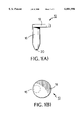
- FIGS. 1(A) and 1(B) are enlarged side elevational and top plan views, respectively, of a through hole connector constructed according to the present invention.
- FIGS. 2(A)-2(D) are enlarged side elevational views showing the steps of the method of the present invention.
- FIGS. 1(A) and 1(B) illustrate a through hole connector, constructed according to the present invention, and indicated generally by the reference numeral 10.
- Connector 10 includes a vertical cylindrical portion 16 and a horizontal offset head portion 18 formed integrally with the vertical cylindrical portion. While a wide range of dimensions may be employed depending on the application, for through hole interconnects in vias, vertical cylindrical portion 16 is preferably about 0.8 mm in diameter, with a length below horizontal offset head portion 18 of about 2.1 mm, and the horizontal offset head portion is about 2 mm in diameter, with a thickness of about 0.3 mm.
- Connector 10 is preferably electronic grade copper or brass, plated with tin/lead solder of 9 microns minimum thickness to optimize and erase electrical conductivity and solderability. Pointed tip 20 (FIG. 1(A)) is arbitrary but eases insertability.
- Such a connector 10 may be solid or hollow and can be conveniently packaged in 8 mm wide by 4 mm pitch tape and reel for use in a conventional pick and place machine
- FIGS. 2(A)-2(D) illustrate the method of manufacture according to the present invention.
- a substrate 30 is provided which, for illustrative purposes, may be assumed to be the substrate for a printed circuit board and through which is defined a circular through hole 32.
- through hole 32 is preferably at least 5 mils greater in diameter than the diameter of vertical cylindrical portion 16.
- An annular conductive pad 36 is placed by conventional means on the lower surface of substrate 30 surrounding and adjacent through hole 32.
- Another conductive pad 40 is placed on the upper surface of substrate 30.
- the portion of conductive pad 40 offset with respect to hole 32 has the same general diameter as offset head 18 (FIG. 1(A)), but is slightly larger in diameter than the offset head.
- a layer 44 of conventional solder paste is placed on the offset portion of conductive pad 40.
- FIG. 2(C) illustrates the elements so far described after the elements have been processed in a conventional reflow step which melts the solder paste.
- horizontal offset head portion 18 and, therefore, pin 10 have been drawn to the right as shown on FIG. 2(C) in the direction of the arrow, with vertical cylindrical portion drawn to the side of through hole 32, leaving open from the top to the bottom of substrate 30 a crescent shaped portion of the through hole.
- the melting step has also formed a solder fillet 50 around the edge of horizontal offset head portion 18 between the offset head portion and conductive pad 40.
- FIG. 2(D) illustrates the elements after a conventional wave soldering operation has been performed during which a solder fillet 60 has been formed connecting the lower end of connector pin 10 and conductive pad 36.
- the open portion of through hole 32 permitted gas to escape in the direction of the arrow on FIG. 2(D), thus preventing the formation of blowholes in solder fillet 60.
- Connector pin 10 can be conveniently and economically cold formed using conventional heading equipment such as that used for the manufacture of nails and plated using standard techniques.
- Horizontal offset head portion 18 (FIG. 1(A)) optimizes pickup and placement by conventional surface mount placement machines and to enable a large solder connection to maximize electronic contact, heat transfer, and surface tension.
- connector pin 10 is designed to carrying a continuous 5 Amperes of current.
Abstract
Description
Claims (1)
Priority Applications (1)
| Application Number | Priority Date | Filing Date | Title |
|---|---|---|---|
| US09/177,586 US6081996A (en) | 1998-10-23 | 1998-10-23 | Through hole circuit board interconnect |
Applications Claiming Priority (1)
| Application Number | Priority Date | Filing Date | Title |
|---|---|---|---|
| US09/177,586 US6081996A (en) | 1998-10-23 | 1998-10-23 | Through hole circuit board interconnect |
Publications (1)
| Publication Number | Publication Date |
|---|---|
| US6081996A true US6081996A (en) | 2000-07-04 |
Family
ID=22649178
Family Applications (1)
| Application Number | Title | Priority Date | Filing Date |
|---|---|---|---|
| US09/177,586 Expired - Lifetime US6081996A (en) | 1998-10-23 | 1998-10-23 | Through hole circuit board interconnect |
Country Status (1)
| Country | Link |
|---|---|
| US (1) | US6081996A (en) |
Cited By (18)
| Publication number | Priority date | Publication date | Assignee | Title |
|---|---|---|---|---|
| WO2002049160A1 (en) * | 2000-12-15 | 2002-06-20 | Di/Dt, Inc. | Circuit module with universal connectivity |
| US6409523B1 (en) * | 2001-06-27 | 2002-06-25 | Jess-Link Products Co., Ltd. | Terminal legs of connectors |
| US6593535B2 (en) * | 2001-06-26 | 2003-07-15 | Teradyne, Inc. | Direct inner layer interconnect for a high speed printed circuit board |
| US20030201123A1 (en) * | 2002-04-30 | 2003-10-30 | Kris Kistner | Electrical connector pad assembly for printed circuit board |
| US6644985B2 (en) * | 2001-02-16 | 2003-11-11 | Fci Americas Technology, Inc. | Ball attached zero insertion force socket |
| US20040092174A1 (en) * | 2002-09-23 | 2004-05-13 | Eichorn Daniel S. | Circuit board inter-connection system and method |
| US6783374B2 (en) * | 1999-12-21 | 2004-08-31 | Murata Manufacturing Co., Ltd. | Electronic component, coaxial connector, and communication device |
| WO2004086831A2 (en) * | 2003-03-26 | 2004-10-07 | Siemens Aktiengesellschaft | Method and device for electrically and mechanically connecting two printed boards |
| US6950644B2 (en) * | 2001-02-21 | 2005-09-27 | Sharp Kabushiki Kaisha | Satellite broadcast receiving device having two local oscillation circuits and reduced spurious signal |
| US7157791B1 (en) * | 2004-06-11 | 2007-01-02 | Bridge Semiconductor Corporation | Semiconductor chip assembly with press-fit ground plane |
| EP1755023A1 (en) * | 2004-05-21 | 2007-02-21 | Nissha Printing Co., Ltd. | Touch panel and electronic device display window protection panel using the same |
| US20070167037A1 (en) * | 2004-02-11 | 2007-07-19 | Conti Temic Microelectronic, Gmbh | Electric sub-assembly comprising an electrically conductive contact pin for pressing into an opening of a printed circuit board |
| US20070184688A1 (en) * | 2006-02-08 | 2007-08-09 | Cesar Avitia | Interconnection device for a double-sided printed circuit board |
| WO2012099602A1 (en) * | 2011-01-21 | 2012-07-26 | Lexmark International, Inc. | Z-directed connector components for printed circuit boards |
| US20120196484A1 (en) * | 2009-10-06 | 2012-08-02 | Nicomatic Sa | Through-Connector For A Metal Structure, And Associated Insulating Component And Metal Stucture |
| CN102892256A (en) * | 2012-09-28 | 2013-01-23 | 广州视睿电子科技有限公司 | Method for mounting electronic element on surface of printed circuit board |
| US20160285182A1 (en) * | 2015-03-25 | 2016-09-29 | Broadband International Inc. | Circuit Assembly Pin |
| US11826861B1 (en) * | 2020-08-12 | 2023-11-28 | Sion Power Corporation | Joining systems, clamping fixtures, and related systems and methods |
Citations (5)
| Publication number | Priority date | Publication date | Assignee | Title |
|---|---|---|---|---|
| GB1397026A (en) * | 1972-03-27 | 1975-06-11 | Bendix Corp | Circuit board and method for manufacturing same |
| DE3134135A1 (en) * | 1981-08-28 | 1983-03-17 | Robert Bosch Gmbh, 7000 Stuttgart | Printed circuit board |
| US4592137A (en) * | 1982-11-27 | 1986-06-03 | Matsushita Electric Industrial Co., Ltd. | Method of circuit connection across both surfaces of substrate |
| US5637835A (en) * | 1995-05-26 | 1997-06-10 | The Foxboro Company | Automatic test detection of unsoldered thru-hole connector leads |
| US5909011A (en) * | 1996-08-01 | 1999-06-01 | International Business Machines Corporation | Method and apparatus for modifying circuit having ball grid array interconnections |
-
1998
- 1998-10-23 US US09/177,586 patent/US6081996A/en not_active Expired - Lifetime
Patent Citations (5)
| Publication number | Priority date | Publication date | Assignee | Title |
|---|---|---|---|---|
| GB1397026A (en) * | 1972-03-27 | 1975-06-11 | Bendix Corp | Circuit board and method for manufacturing same |
| DE3134135A1 (en) * | 1981-08-28 | 1983-03-17 | Robert Bosch Gmbh, 7000 Stuttgart | Printed circuit board |
| US4592137A (en) * | 1982-11-27 | 1986-06-03 | Matsushita Electric Industrial Co., Ltd. | Method of circuit connection across both surfaces of substrate |
| US5637835A (en) * | 1995-05-26 | 1997-06-10 | The Foxboro Company | Automatic test detection of unsoldered thru-hole connector leads |
| US5909011A (en) * | 1996-08-01 | 1999-06-01 | International Business Machines Corporation | Method and apparatus for modifying circuit having ball grid array interconnections |
Non-Patent Citations (2)
| Title |
|---|
| IBM Techincal Disclosure Bullentin, vol. 8, No. 11, "Module Terminal Pin and Land Structure", J.A. Antenucci, Apr. 1966. |
| IBM Techincal Disclosure Bullentin, vol. 8, No. 11, Module Terminal Pin and Land Structure , J.A. Antenucci, Apr. 1966. * |
Cited By (29)
| Publication number | Priority date | Publication date | Assignee | Title |
|---|---|---|---|---|
| US6783374B2 (en) * | 1999-12-21 | 2004-08-31 | Murata Manufacturing Co., Ltd. | Electronic component, coaxial connector, and communication device |
| US6692269B2 (en) * | 2000-12-15 | 2004-02-17 | Di/Dt, Inc. | Circuit module with universal connectivity |
| WO2002049160A1 (en) * | 2000-12-15 | 2002-06-20 | Di/Dt, Inc. | Circuit module with universal connectivity |
| US6644985B2 (en) * | 2001-02-16 | 2003-11-11 | Fci Americas Technology, Inc. | Ball attached zero insertion force socket |
| US6950644B2 (en) * | 2001-02-21 | 2005-09-27 | Sharp Kabushiki Kaisha | Satellite broadcast receiving device having two local oscillation circuits and reduced spurious signal |
| US6593535B2 (en) * | 2001-06-26 | 2003-07-15 | Teradyne, Inc. | Direct inner layer interconnect for a high speed printed circuit board |
| US6409523B1 (en) * | 2001-06-27 | 2002-06-25 | Jess-Link Products Co., Ltd. | Terminal legs of connectors |
| US6828513B2 (en) | 2002-04-30 | 2004-12-07 | Texas Instruments Incorporated | Electrical connector pad assembly for printed circuit board |
| US20030201123A1 (en) * | 2002-04-30 | 2003-10-30 | Kris Kistner | Electrical connector pad assembly for printed circuit board |
| US20040092174A1 (en) * | 2002-09-23 | 2004-05-13 | Eichorn Daniel S. | Circuit board inter-connection system and method |
| US7025640B2 (en) | 2002-09-23 | 2006-04-11 | Delphi Technologies, Inc. | Circuit board inter-connection system and method |
| WO2004086831A2 (en) * | 2003-03-26 | 2004-10-07 | Siemens Aktiengesellschaft | Method and device for electrically and mechanically connecting two printed boards |
| WO2004086831A3 (en) * | 2003-03-26 | 2005-03-17 | Siemens Ag | Method and device for electrically and mechanically connecting two printed boards |
| US20070167037A1 (en) * | 2004-02-11 | 2007-07-19 | Conti Temic Microelectronic, Gmbh | Electric sub-assembly comprising an electrically conductive contact pin for pressing into an opening of a printed circuit board |
| EP1755023A1 (en) * | 2004-05-21 | 2007-02-21 | Nissha Printing Co., Ltd. | Touch panel and electronic device display window protection panel using the same |
| EP1755023A4 (en) * | 2004-05-21 | 2008-10-29 | Nissha Printing | Touch panel and electronic device display window protection panel using the same |
| US7830367B2 (en) * | 2004-05-21 | 2010-11-09 | Nissha Printing Co., Ltd. | Touch panel and protective panel for display window of electronic device using the same |
| US20070218957A1 (en) * | 2004-05-21 | 2007-09-20 | Kazuhiro Nishikawa | Touch Panel And Protective Panel For Display Window Of Electronic Device Using The Same |
| US7157791B1 (en) * | 2004-06-11 | 2007-01-02 | Bridge Semiconductor Corporation | Semiconductor chip assembly with press-fit ground plane |
| DE102007005824B4 (en) * | 2006-02-08 | 2009-02-05 | Visteon Global Technologies Inc., Van Buren | Connecting element for a double-sided circuit board |
| GB2435350B (en) * | 2006-02-08 | 2008-04-02 | Visteon Global Tech Inc | Interconnection device for a double-sided printed circuit board |
| GB2435350A (en) * | 2006-02-08 | 2007-08-22 | Visteon Global Tech Inc | Interconnection device for a double sided PCB |
| US20070184688A1 (en) * | 2006-02-08 | 2007-08-09 | Cesar Avitia | Interconnection device for a double-sided printed circuit board |
| US20120196484A1 (en) * | 2009-10-06 | 2012-08-02 | Nicomatic Sa | Through-Connector For A Metal Structure, And Associated Insulating Component And Metal Stucture |
| WO2012099602A1 (en) * | 2011-01-21 | 2012-07-26 | Lexmark International, Inc. | Z-directed connector components for printed circuit boards |
| CN102892256A (en) * | 2012-09-28 | 2013-01-23 | 广州视睿电子科技有限公司 | Method for mounting electronic element on surface of printed circuit board |
| US20160285182A1 (en) * | 2015-03-25 | 2016-09-29 | Broadband International Inc. | Circuit Assembly Pin |
| US10439310B2 (en) * | 2015-03-25 | 2019-10-08 | Edward Perez | Circuit assembly pin |
| US11826861B1 (en) * | 2020-08-12 | 2023-11-28 | Sion Power Corporation | Joining systems, clamping fixtures, and related systems and methods |
Similar Documents
| Publication | Publication Date | Title |
|---|---|---|
| US6081996A (en) | Through hole circuit board interconnect | |
| US8397977B2 (en) | Solder containment brackets | |
| US7637415B2 (en) | Methods and apparatus for assembling a printed circuit board | |
| JP2006164979A (en) | Improved fuse having spread solder | |
| EP3084886B1 (en) | A connection pin, a converter assembly and a method for manufacturing a connection pin | |
| JP2004207232A (en) | Solder storage transferring device and step | |
| US3500538A (en) | Method for producing a wire having improved soldering characteristics | |
| US6881906B2 (en) | Printed circuit board comprising a contact sleeve that is mounted thereon | |
| CA2214130A1 (en) | Assemblies of substrates and electronic components | |
| US5455741A (en) | Wire-lead through hole interconnect device | |
| US4592137A (en) | Method of circuit connection across both surfaces of substrate | |
| US5468919A (en) | Printed circuit board device with surface-mounted bar-like connectors | |
| US6207298B1 (en) | Connector surface-treated with a Sn-Ni alloy | |
| US20050064745A1 (en) | Terminal for electrical connector | |
| US7057293B2 (en) | Structure comprising a printed circuit board with electronic components mounted thereon and a method for manufacturing the same | |
| JP2926902B2 (en) | Printed wiring board | |
| US20070184688A1 (en) | Interconnection device for a double-sided printed circuit board | |
| JP2546613Y2 (en) | Chip type capacitors | |
| JP3273239B2 (en) | Surface mount type connector | |
| JPH03262186A (en) | Printed wiring board | |
| US20180332705A1 (en) | Printed circuit board structure | |
| JPH11220231A (en) | Resin molded substrate | |
| JP4330013B2 (en) | Manufacturing method of electric component mounting board | |
| JP2003224356A (en) | Printed wiring board with edge face cut through-hole and electronic component | |
| JPS6151945A (en) | Semiconductor device |
Legal Events
| Date | Code | Title | Description |
|---|---|---|---|
| AS | Assignment |
Owner name: DELCO ELECTRONICS CORPORATION, INDIANA Free format text: ASSIGNMENT OF ASSIGNORS INTEREST;ASSIGNORS:KRUPPA, VICTOR DAVID;DANTZLER, MAURICE LYDELL;VOLTENBURG, ROBERT RAY, JR.;REEL/FRAME:009543/0235;SIGNING DATES FROM 19981002 TO 19981012 |
|
| STCF | Information on status: patent grant |
Free format text: PATENTED CASE |
|
| FPAY | Fee payment |
Year of fee payment: 4 |
|
| AS | Assignment |
Owner name: DELPHI TECHNOLOGIES, INC., MICHIGAN Free format text: ASSIGNMENT OF ASSIGNORS INTEREST;ASSIGNOR:DELCO ELECTRONICS CORPORATION;REEL/FRAME:016700/0623 Effective date: 20050701 |
|
| AS | Assignment |
Owner name: JPMORGAN CHASE BANK, N.A., TEXAS Free format text: SECURITY AGREEMENT;ASSIGNOR:DELPHI TECHNOLOGIES, INC.;REEL/FRAME:016237/0402 Effective date: 20050614 |
|
| FPAY | Fee payment |
Year of fee payment: 8 |
|
| AS | Assignment |
Owner name: DELPHI TECHNOLOGIES, INC., MICHIGAN Free format text: RELEASE OF SECURITY AGREEMENT;ASSIGNOR:JPMORGAN CHASE BANK, N.A.;REEL/FRAME:020808/0583 Effective date: 20080225 |
|
| AS | Assignment |
Owner name: PEAKS ISLAND LLC, DELAWARE Free format text: ASSIGNMENT OF ASSIGNORS INTEREST;ASSIGNOR:DELPHI TECHNOLOGIES, INC.;REEL/FRAME:026459/0909 Effective date: 20110113 |
|
| FPAY | Fee payment |
Year of fee payment: 12 |
|
| AS | Assignment |
Owner name: RPX CORPORATION, CALIFORNIA Free format text: ASSIGNMENT OF ASSIGNORS INTEREST;ASSIGNOR:PEAKS ISLAND LLC;REEL/FRAME:028146/0045 Effective date: 20120420 |
|
| AS | Assignment |
Owner name: JEFFERIES FINANCE LLC, NEW YORK Free format text: SECURITY INTEREST;ASSIGNOR:RPX CORPORATION;REEL/FRAME:046486/0433 Effective date: 20180619 |
|
| AS | Assignment |
Owner name: RPX CORPORATION, CALIFORNIA Free format text: RELEASE BY SECURED PARTY;ASSIGNOR:JEFFERIES FINANCE LLC;REEL/FRAME:054486/0422 Effective date: 20201023 |