US6112291A - Method and apparatus for performing a shift instruction with saturate by examination of an operand prior to shifting - Google Patents
Method and apparatus for performing a shift instruction with saturate by examination of an operand prior to shifting Download PDFInfo
- Publication number
- US6112291A US6112291A US09/012,325 US1232598A US6112291A US 6112291 A US6112291 A US 6112291A US 1232598 A US1232598 A US 1232598A US 6112291 A US6112291 A US 6112291A
- Authority
- US
- United States
- Prior art keywords
- circuitry
- operand
- source operand
- destination
- bits
- Prior art date
- Legal status (The legal status is an assumption and is not a legal conclusion. Google has not performed a legal analysis and makes no representation as to the accuracy of the status listed.)
- Expired - Lifetime
Links
- 238000000034 method Methods 0.000 title claims description 16
- 230000015654 memory Effects 0.000 claims abstract description 27
- 238000012545 processing Methods 0.000 claims description 28
- 230000004044 response Effects 0.000 claims description 18
- 238000001514 detection method Methods 0.000 claims description 10
- 229920006395 saturated elastomer Polymers 0.000 abstract description 7
- 238000009738 saturating Methods 0.000 abstract 1
- 101150022676 CSTB gene Proteins 0.000 description 12
- 101100534231 Xenopus laevis src-b gene Proteins 0.000 description 12
- 238000010586 diagram Methods 0.000 description 8
- 230000002093 peripheral effect Effects 0.000 description 5
- 235000019800 disodium phosphate Nutrition 0.000 description 4
- 230000008901 benefit Effects 0.000 description 3
- 238000012360 testing method Methods 0.000 description 2
- 238000010276 construction Methods 0.000 description 1
- 238000003384 imaging method Methods 0.000 description 1
- 238000004519 manufacturing process Methods 0.000 description 1
- 238000012986 modification Methods 0.000 description 1
- 230000004048 modification Effects 0.000 description 1
- 238000010606 normalization Methods 0.000 description 1
Images


Classifications
-
- G—PHYSICS
- G06—COMPUTING; CALCULATING OR COUNTING
- G06F—ELECTRIC DIGITAL DATA PROCESSING
- G06F9/00—Arrangements for program control, e.g. control units
- G06F9/06—Arrangements for program control, e.g. control units using stored programs, i.e. using an internal store of processing equipment to receive or retain programs
- G06F9/30—Arrangements for executing machine instructions, e.g. instruction decode
- G06F9/30003—Arrangements for executing specific machine instructions
- G06F9/30007—Arrangements for executing specific machine instructions to perform operations on data operands
- G06F9/30032—Movement instructions, e.g. MOVE, SHIFT, ROTATE, SHUFFLE
Definitions
- This invention relates to microprocessors, and particularly relates to architectures of very long instruction word processors.
- Microprocessor designers have increasingly endeavored to improve performance in various microprocessors by increasing clock speeds and adding parallelism. Complex data manipulations require execution of a number of instructions, which may require several iterative cycles for various types of data manipulations. Some microprocessors contain special instructions for specific types of data manipulations, but these generally require a number of microcode cycles for execution.
- An object of the present invention is to overcome the performance delay caused by iterative execution of microcode for a shift instruction when an operand becomes saturated.
- a data processing device for executing an instruction which shifts a source operand a specified number of bits and saturates the result if a numerical overflow would result from the shift.
- the device has source circuitry which provides a source operand, destination circuitry to receive a destination operand, and circuitry to hold a constant which specifies the number of bits to shift the source operand.
- Setting circuitry forms the destination operand by setting all bits within the destination to represent a most positive or a most negative number in a single instruction execution phase.
- a method for executing an instruction within a data processing device which shifts a source operand a predetermined number of bits comprises the steps of: providing the source operand; holding a first constant responsive to the shift instruction which indicates the number of bits to shift the source operand; and forming a destination operand by setting all bits in the destination operand to a predetermined value in response to the shift instruction if a set of most significant bits in the source operand corresponding to the first constant are not uniform.
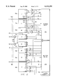
- FIG. 1 is a block diagram of a microprocessor which has an embodiment of the present invention
- FIG. 2 is a block diagram of the execution units and register files of the microprocessor of FIG. 1;
- FIG. 3A is a chart which illustrates the processing phases of an instruction execution pipeline in the microprocessor of FIG. 1;
- FIG. 3B is a chart which illustrates the execution phases of the instruction execution pipeline in the microprocessor of FIG. 1;
- FIG. 4 is a timing diagram which illustrates timing details of processing an instruction fetch packet during the processing phases of FIG. 3A and execution of the execution packet during the execution phases of FIG. 3B;
- FIGS. 5A and 5B illustrate opcode forms for a Shift Left with Saturate instruction for the microprocessor of FIG. 1;
- FIGS. 6A-6D illustrate the operation of the Shift Left with Saturate instruction of FIGS. 5A-5B;
- FIG. 7 is a block diagram of logic to implement the Shift Left with Saturate instructions of FIGS. 5A-6D;
- FIG. 8A is a schematic of the msb mask generation circuitry of FIG. 7;
- FIG. 8B is a schematic of the detection circuitry of FIG. 7.
- FIG. 8C is a schematic of setting circuitry of FIG. 7.
- FIG. 1 is a block diagram of a microprocessor 1 which has an embodiment of the present invention.
- Microprocessor 1 is a VLIW digital signal processor ("DSP").
- DSP VLIW digital signal processor
- FIG. 1 only shows those portions of microprocessor 1 that are relevant to an understanding of an embodiment of the present invention. Details of general construction for DSPs are well known, and may be found readily elsewhere. For example, U.S. Pat. No. 5,072,418 issued to Frederick Boutaud, et al, describes a DSP in detail and is incorporated herein by reference. U.S. Pat. No. 5,329,471 issued to Gary Swoboda, et al, describes in detail how to test and emulate a DSP and is incorporated herein by reference. Details of portions of microprocessor 1 relevant to an embodiment of the present invention are explained in sufficient detail hereinbelow, so as to enable one of ordinary skill in the microprocessor art to make and use the invention.
- CPU 10 central processing unit
- CPU 10 data memory 22, program memory 23, peripherals 60 and an external memory interface (EMIF) with a direct memory access (DMA) 61.
- CPU 10 further has an instruction fetch/decode unit 10a-c, a plurality of execution units, including an arithmetic and load/store unit D1, a multiplier M1, an ALU/shifter unit S1, an arithmetic logic unit (“ALU") L1, a shared multiport register file 20a from which data are read and to which data are written.
- Decoded instructions are provided from the instruction fetch/decode unit 10a-c to the functional units D1, M1, S1, and L1 over various sets of control lines which are not shown.
- Data are provided to/from the register file 20a from/to to load/store units D1 over a first set of busses 32a, to multiplier M1 over a second set of busses 34a, to ALU/shifter unit S1 over a third set of busses 36a and to ALU L1 over a fourth set of busses 38a.
- Data are provided to/from the memory 22 from/to the load/store units D1 via a fifth set of busses 40a. Note that the entire data path described above is duplicated with register file 20b and execution units D2, M2, S2, and L2. Instructions are fetched by fetch unit 10a from instruction memory 23 over a set of busses 41.
- Emulation unit 50 provides access to the internal operation of integrated circuit 1 which can be controlled by an external test system 51.
- memory 22 and memory 23 are shown in FIG. 1 to be a part of a microprocessor 1 integrated circuit, the extent of which is represented by the box 42.
- the memories 22-23 could just as well be external to the microprocessor 1 integrated circuit 42, or part of it could reside on the integrated circuit 42 and part of it be external to the integrated circuit 42. Also, an alternate number of execution units can be used.
- RAM Random Access Memory
- ROM Read Only Memory
- Disk 72 Disk 72
- Bus 73 is connected to the External Memory Interface (EMIF) which is part of functional block 61 within microprocessor 42.
- EMIF External Memory Interface
- DMA Direct Memory Access
- the DMA controller is generally used to move data between memory and peripherals within microprocessor 1 and memory and peripherals which are external to microprocessor 1.
- a description of various architectural features of the microprocessor of FIG. 1 is provided in coassigned application Ser. No. 09/012,813 (TI docket number T-25311).
- a description of a complete set of instructions for the microprocessor of FIG. 1 is also provided in coassigned application Ser. No. 09/012,813 (TI docket number T-25311).
- FIG. 2 is a block diagram of the execution units and register files of the microprocessor of FIG. 1 and shows a more detailed view of the buses connecting the various functional blocks.
- Bus 40a has an address bus DA1 which is driven by mux 200a. This allows an address generated by either load/store unit D1 or D2 to provide an address for loads or stores for register file 20a.
- Data Bus LD1 roads data from an address in memory 22 specified by address bus DA1 to a register in load unit D1. Unit D1 may manipulate the data provided prior to storing it in register file 20a.
- data bus ST1 stores data from register file 20a to memory 22.
- Load/store unit D1 performs the following operations: 32-bit add, subtract, linear and circular address calculations.
- Load/store unit D2 operates similarly to unit D1, with the assistance of mux 200b for selecting an address.
- ALU unit L1 performs the following types of operations: 32/40 bit arithmetic and compare operations; left most 1, 0, bit counting for 32 bits; normalization count for 32 and 40 bits; and logical operations.
- ALU L1 has input src1 for a 32 bit source operand and input src2 for a second 32 bit source operand.
- Input msb -- src is an 8 bit value used to form 40 bit source operands.
- ALU L1 has an output dst for a 32 bit destination operands.
- Output msb -- dst is an 8 bit value used to form 40 bit destination operands.
- Two 32 bit registers in register file 20a are concatenated to hold a 40 bit operand.
- Mux 211 is connected to input src1 and allows a 32 bit operand to be obtained from register file 20a via bus 38a or from register file 20b via bus 210.
- Mux 212 is connected to input src2 and allows a 32 bit operand to be obtained from register file 20a via bus 38a or from register file 20b via bus 210.
- ALU unit L2 operates similarly to unit L1.
- ALU/shifter unit S1 performs the following types of operations: 32 bit arithmetic operations; 32/40 bit shifts and 32 bit bit-field operations; 32 bit logical operations; branching; and constant generation.
- ALU S1 has input src1 for a 32 bit source operand and input src2 for a second 32 bit source operand.
- Input msb -- src is an 8 bit value used to form 40 bit source operands.
- ALU S1 has an output dst for a 32 bit destination operands.
- Output msb -- dst is an 8 bit value used to form 40 bit destination operands.
- Mux 213 is connected to input src2 and allows a 32 bit operand to be obtained from register file 20a via bus 36a or from register file 20b via bus 210.
- ALU unit S2 operates similarly to unit S1, but can additionally perform register transfers to/from the control register file 102.
- Multiplier M1 performs 16 ⁇ 16 multiplies.
- Multiplier M1 has input src1 for a 32 bit source operand and input src2 for a 32 bit source operand.
- ALU S1 has an output dst for a 32 bit destination operands.
- Mux 214 is connected to input src2 and allows a 32 bit operand to be obtained from register file 20a via bus 34a or from register file 20b via bus 210.
- Multiplier M2 operates similarly to multiplier M1.
- FIG. 3A is a chart which illustrates the processing phases of an instruction execution pipeline in the microprocessor of FIG. 1.
- Each phase corresponds roughly to a clock cycle of a system clock. For example, if microprocessor 1 is being operated at 200 MHz, then each phase is nominally 5 Ns. However, in a phase where data is expected from a memory or peripheral, such as RAM 70, the pipeline will stall if the data is not ready when expected. When stalled, a given pipeline phase will exist for a number of system clock cycles.
- the first phase of processing an instruction is to generate the program address in phase PG. This is done by loading a program fetch counter PFC which is located in control register file 102.
- an address of an instruction fetch packet is sent to program memory 23 via a program address bus PADDR which is part of bus 41.
- the third phase PW is a wait phase to allow for access time in memory 23.
- a program fetch packet is available from program memory 23 via data bus PDATA -- I which is part of bus 41.
- instruction parallelism is detected and instructions that can be executed are dispatched to the appropriate functional units. This aspect of pipeline operation will be described in more detail in later paragraphs.
- executable instructions are decoded and control signals are generated to control the various data paths and functional units.
- FIG. 3B is a chart which illustrates the execution phases of the instruction execution pipeline in the microprocessor of FIG. 1.
- first execution phase E1 single cycle instructions, referred to as "ISC", and branch instructions, referred to as "BR" are completed.
- a designated execution unit performs the operations indicated in FIG. 3B as directed by control circuitry 100.
- second execution phase E2 the following types of instructions are completed by designated execution units under control of control circuitry 100: integer multiply (IMPY), program store instructions (STP), and data store instructions (STD).
- IMPY integer multiply
- STP program store instructions
- STD data store instructions
- LD load data instructions
- DMS data memory system
- execution phase E4 the data latched in E3 is transferred to a data input register DDATA -- I in execution unit D1 or D2.
- execution phase E5 the LD instruction is completed by manipulating the data in register DDATA -- I and writing the manipulated data to a specified register in register file 20a or 20b.
- FIG. 4 is a timing diagram which illustrates timing details of processing an instruction fetch packet during the processing phases of FIG. 3A and execution of the execution packet during the execution phases of FIG. 3B. Note that a pipe stall is illustrated in phase PW due to a program memory ready signal PRDY being low in phase PS, and a second pipe stall in phase E3 due a data memory ready signal DRDY being low in phase E2.
- FIGS. 5A and 5B illustrate opcode forms for a Shift Left with Saturate instruction for the microprocessor of FIG. 1.
- FIG. 5A shows a form of the instruction in which the number of bits to shift the operand is specified by a constant field in the instruction itself.
- a destination field dst specifies a destination register in register file 20a which receives the result operand of the instruction.
- a source field src2 specifies a register in register file 20a which holds a source operand which is to be shifted. If bit field "x" is a one, then source field src2 specifies a register in register file 20b.
- a constant field cstb specifies the number of bits to be shifted.
- FIG. 5B shows a form of the instruction in which the number of bits to be shifted is specified by two fields in a register in register file 20a which is designated by the instruction. The five least significant bits in the specified register are used to specify the shift count. Otherwise, the operation of both forms to the instruction is the same.
- FIGS. 6A-6D illustrate the operation of the Shift Left with Saturate instruction of FIGS. 5A-5B.
- a Shift Left with Saturate instruction When a Shift Left with Saturate instruction is executed, a source operand stored in a register specified by the source field src2 is selected by execution unit S1. The specified source operand is shifted left by the specified number of bits within execution unit S1. A copy of the modified source operand is then written to a register specified by the destination field dst. However, if the results of the shift operation would result in numerical overflow, then a saturated value is written to the destination register.
- the instruction may be executed on execution unit S2 using register file 20b by setting bit "s" in the instruction to a 1. According to an aspect of the present invention, this entire execution operation is advantageously performed in a single execution phase E1 of the instruction execution pipeline of CPU 10.
- detection circuitry which examines the source operand before it is shifted advantageously eliminates the need to monitor the lost bits during the shift operation. Furthermore, it has been discovered that if all of the bits which are between source operand bit 31 and source operand bit(31-shift -- count) are either all ones or all zeros, then no overflow will occur as a result of the shift.
- FIGS. 6A-6D illustrate a shift in which the shift count, field cstb, is eleven.
- bits 0-20 of the specified source operand are shifted left by eleven bits so that source operand bit 20 ends up as destination bit 31.
- Source operand bit(31-shift -- vcount) is thus bit(31-11), or bit 20.
- the source operand has zeros in at least bits 20-31. According to an aspect of the present invention, by determining that bits 20-31 are all zeros implies that no overflow will occur when the source operand indicated in FIG. 6A is shifted left eleven bits.
- the source operand has ones in at least bits 20-31. According to an aspect of the present invention, by determining that bits 20-31 are all ones implies that no overflow will occur when the source operand indicated in FIG. 6B is shifted left eleven bits.
- the source operand has ones in at least bits 20-31, except for bit 26 which is a zero. According to an aspect of the present invention, by determining that bits 20-31 are not all ones implies that an overflow will occur when the source operand indicated in FIG. 6C is shifted left eleven bits. Therefore, since the source operand is a negative number, the destination operand is saturated with the largest negative number, 8000 0000h (hexadecimal).
- the source operand has zeros in at least bits 20-31, except for bit 26 which is a one. According to an aspect of the present invention, by determining that bits 20-31 are not all zeros implies that an overflow will occur when the source operand indicated in FIG. 6D is shifted left eleven bits. Therefore, since the source operand is a positive number, the destination operand is saturated with the largest positive number, 7FFF FFFFh.
- FIG. 7 is a block diagram of saturation circuitry 400 to implement the Shift Left with Saturate instructions of FIGS. 5A-6D in a single instruction execution pipeline phase.
- Saturation circuitry 400 of FIG. 7 is incorporated into execution units S1 and S2 in CPU 10.
- source operand circuitry 401 is the register selected by source field src2 in a Shift Left with Saturate instruction.
- destination operand circuitry 402 is the register selected by destination field dst in the Shift Left with Saturate instruction.
- Constant-B holding circuitry 403 hold the data from field cstb from an instruction during execution or from a source register specified by the instruction, as discussed with regard to FIGS. 5A-5B. The output of holding circuitry 403 is inverted, so that an inverted version of constant-B is provided to circuitry 410; Thus, when a shift count of 11, for example, is specified by constant-B, a bit position of bit-20 is specified by the inverted field cstb.
- Most significant bit (msb) mask generation circuitry 410 forms a 32 bit mask based on a number specified by constant field cstb from the instruction or from the register specified by source field src1 in the instruction.
- the msb mask has a 1 in all bit positions which are more significant than or equal to the bit position specified by inverted constant cstb.
- the msb mask has a 0 in all bit positions which are less significant than the bit position specified by inverted constant cstb.
- Detection circuitry 420 determines when bits in the source operand in bit positions corresponding to ones in the msb mask are all ones or all zeros. If this condition is not true, then saturate signal 421 is asserted. When saturate signal 421 is asserted, a saturate status bit 450 is set to indicate that a saturate condition has occurred.
- Setting circuitry 430 writes a 7FFF FFFF into destination circuitry 402 when saturate signal 421 is asserted and the source operand is positive. Setting circuitry 430 writes a 8000 0000 into destination circuitry 402 when saturate signal 421 is asserted and the source operand is negative. Otherwise, shift circuitry 440 shifts the specified operand by the specified number of bits and writes the results into destination circuitry 402 in one execution phase; phase E1.
- FIG. 8A is a schematic of the msb mask generation circuitry 410 of FIG. 7.
- the msb mask has a 1 in all bit positions which are more significant than or equal to the bit position specified by inverted constant cstb.
- the msb mask has a 0 in all bit positions which are less significant than the bit position specified by inverted constant cstb.
- Inverted constant cstb is a 5 bit constant represented by signals cstb0-cstb4.
- AND-OR gate 800 receives signal 860 which is 1 if signals cstb2-cstb4 are 1, as determined by NAND gate 840.
- Gate 800 also receives signal 855 which is a 1 if signals cstb0-cstb1 are both 1, as determined by NAND gate 854. Thus, the output of gate 800, signal B31 -- bz, is a 0 if cstb is a 11111b which corresponds to a shift count of 0, otherwise signal B31 -- z is a 1. LSBmask signals B(0-30) -- z are formed in a similar manner.
- FIG. 8B is a schematic of detection circuitry 420 of FIG. 7.
- Signals IN0-IN31 correspond to respective bits of a source operand specified by source operand field src2 of a Shift Left with Saturate instruction.
- Signals B(0-31) -- z are the LSB mask from LSB mask circuitry 410.
- Gates 900 and 901 are representative comparison circuitry and are repeated for each bit position. For each bit position where a LSB mask signal B(0-31) -- z is 0, an output signal COMP0-COMP31 is a 1. For each bit position where a LSB mask signal B(0-31) -- z is 1, the operand signal IN0-IN31 for that bit position is compared to the operand signal from the next least significant bit position.
- Gates 920-933 monitor all 32 COMP0-31 signals. If any one of them is 0, then low-true signal SATURATE -- z is asserted (by being 0) to indicate that a destination operand should be saturated in response to executing a Shift Left with Saturate instruction.
- FIG. 8C is a schematic of setting circuitry 430 of FIG. 7.
- Constant generator circuitry 950 forms a constant number with a value of 7FFF FFFFb, representing the largest positive number that can be represented in this numerical notation.
- Constant generator circuitry 951 forms a constant number with a value of 8000 0000b, representing the largest negative number that can be represented in this numerical notation.
- Mux 952 is operable to select constant 950 when signal IN31 is a 0 indicating the source operand is positive, and to select constant 951 when IN31 is 1 indicating the source operand is negative.
- a 32-bit output from mux 952 is provided to mux 953.
- Mux 953 is operable to select the output of mux 952 when the SATURATE -- z signal 421 from detection circuitry 420 is asserted (low) to indicate a saturated destination operand is to be formed. Mux 953 is operable to select shifted operand signals SHT(0-31) from shift circuitry 440 when SATURATE -- z signal 421 from detection circuitry 420 is not asserted (high) to indicate a destination operand is to be formed from the results of shifting a source operand specified by field src2 in a Shift Left with Saturate instruction.
- the entire process of forming an LSB mask, detecting a saturate condition, providing a predetermined constant number and shifting a source operand are performed in one execution phase, phase E1, of the instruction execution pipeline of microprocessor 10.
- Saturate status bit 450 is set at the end of the following instruction execution phase, phase E2.
- An alternative embodiment of the novel aspects of the present invention may include other circuitries which are combined with the circuitries disclosed herein in order to reduce the total gate count of the combined circuitry. Since those skilled in the art are aware of techniques for gate minimization, the details of such an embodiment will not be described herein.
- connection means electrically connected, including where additional elements may be in the electrical connection path.
Abstract
A microprocessor 1 has an instruction fetch/decode unit 10a-c, a plurality of execution units, including an arithmetic and load/store unit D1, a multiplier M1, an ALU/shifter unit S1, an arithmetic logic unit ("ALU") L1, a shared multiport register file 20a from which data are read and to which data are written, and a memory 22. The microprocessor can execute an instruction which shifts a source operand a specified number of bits and saturates the result if a numerical overflow would result from the shift. Execution unit S1 has circuitry for saturating a destination operand by setting all bits within the destination to represent a most positive or a most negative number in a same single instruction execution phase in which the shift would have occurred if not for the overflow. The saturation circuitry examines the source operand prior to shifting to determine if the destination should be saturated.
Description
This application claims benefit of Provisional Application Ser. No. 60/036,225, filed Jan. 24, 1997.
This application is related to coassigned application Ser. No. 09/012,813 filed contemporaneously herewith and incorporated herein by reference.
This invention relates to microprocessors, and particularly relates to architectures of very long instruction word processors.
Microprocessor designers have increasingly endeavored to improve performance in various microprocessors by increasing clock speeds and adding parallelism. Complex data manipulations require execution of a number of instructions, which may require several iterative cycles for various types of data manipulations. Some microprocessors contain special instructions for specific types of data manipulations, but these generally require a number of microcode cycles for execution.
An object of the present invention is to overcome the performance delay caused by iterative execution of microcode for a shift instruction when an operand becomes saturated.
In general, and in a form of the present invention, a data processing device is provided for executing an instruction which shifts a source operand a specified number of bits and saturates the result if a numerical overflow would result from the shift. The device has source circuitry which provides a source operand, destination circuitry to receive a destination operand, and circuitry to hold a constant which specifies the number of bits to shift the source operand. Setting circuitry forms the destination operand by setting all bits within the destination to represent a most positive or a most negative number in a single instruction execution phase.
In another form of the present invention, a method for executing an instruction within a data processing device which shifts a source operand a predetermined number of bits comprises the steps of: providing the source operand; holding a first constant responsive to the shift instruction which indicates the number of bits to shift the source operand; and forming a destination operand by setting all bits in the destination operand to a predetermined value in response to the shift instruction if a set of most significant bits in the source operand corresponding to the first constant are not uniform.
Other embodiments of the present invention will be evident from the description and drawings.
Other features and advantages of the present invention will become apparent by reference to the following detailed description when considered in conjunction with the accompanying drawings, in which:
FIG. 1 is a block diagram of a microprocessor which has an embodiment of the present invention;
FIG. 2 is a block diagram of the execution units and register files of the microprocessor of FIG. 1;
FIG. 3A is a chart which illustrates the processing phases of an instruction execution pipeline in the microprocessor of FIG. 1;
FIG. 3B is a chart which illustrates the execution phases of the instruction execution pipeline in the microprocessor of FIG. 1;
FIG. 4 is a timing diagram which illustrates timing details of processing an instruction fetch packet during the processing phases of FIG. 3A and execution of the execution packet during the execution phases of FIG. 3B;
FIGS. 5A and 5B illustrate opcode forms for a Shift Left with Saturate instruction for the microprocessor of FIG. 1;
FIGS. 6A-6D illustrate the operation of the Shift Left with Saturate instruction of FIGS. 5A-5B;
FIG. 7 is a block diagram of logic to implement the Shift Left with Saturate instructions of FIGS. 5A-6D;
FIG. 8A is a schematic of the msb mask generation circuitry of FIG. 7;
FIG. 8B is a schematic of the detection circuitry of FIG. 7; and
FIG. 8C is a schematic of setting circuitry of FIG. 7.
Corresponding numerals and symbols in the different figures and tables refer to corresponding parts unless otherwise indicated.
FIG. 1 is a block diagram of a microprocessor 1 which has an embodiment of the present invention. Microprocessor 1 is a VLIW digital signal processor ("DSP"). In the interest of clarity, FIG. 1 only shows those portions of microprocessor 1 that are relevant to an understanding of an embodiment of the present invention. Details of general construction for DSPs are well known, and may be found readily elsewhere. For example, U.S. Pat. No. 5,072,418 issued to Frederick Boutaud, et al, describes a DSP in detail and is incorporated herein by reference. U.S. Pat. No. 5,329,471 issued to Gary Swoboda, et al, describes in detail how to test and emulate a DSP and is incorporated herein by reference. Details of portions of microprocessor 1 relevant to an embodiment of the present invention are explained in sufficient detail hereinbelow, so as to enable one of ordinary skill in the microprocessor art to make and use the invention.
In microprocessor 1 there are shown a central processing unit (CPU) 10, data memory 22, program memory 23, peripherals 60 and an external memory interface (EMIF) with a direct memory access (DMA) 61. CPU 10 further has an instruction fetch/decode unit 10a-c, a plurality of execution units, including an arithmetic and load/store unit D1, a multiplier M1, an ALU/shifter unit S1, an arithmetic logic unit ("ALU") L1, a shared multiport register file 20a from which data are read and to which data are written. Decoded instructions are provided from the instruction fetch/decode unit 10a-c to the functional units D1, M1, S1, and L1 over various sets of control lines which are not shown. Data are provided to/from the register file 20a from/to to load/store units D1 over a first set of busses 32a, to multiplier M1 over a second set of busses 34a, to ALU/shifter unit S1 over a third set of busses 36a and to ALU L1 over a fourth set of busses 38a. Data are provided to/from the memory 22 from/to the load/store units D1 via a fifth set of busses 40a. Note that the entire data path described above is duplicated with register file 20b and execution units D2, M2, S2, and L2. Instructions are fetched by fetch unit 10a from instruction memory 23 over a set of busses 41. Emulation unit 50 provides access to the internal operation of integrated circuit 1 which can be controlled by an external test system 51.
Note that the memory 22 and memory 23 are shown in FIG. 1 to be a part of a microprocessor 1 integrated circuit, the extent of which is represented by the box 42. The memories 22-23 could just as well be external to the microprocessor 1 integrated circuit 42, or part of it could reside on the integrated circuit 42 and part of it be external to the integrated circuit 42. Also, an alternate number of execution units can be used.
When microprocessor 1 is incorporated in a data processing system, additional memory or peripherals may be connected to microprocessor 1, as illustrated in FIG. 1. For example, Random Access Memory (RAM) 70, a Read Only Memory (ROM) 71 and a Disk 72 are shown connected via an external bus 73. Bus 73 is connected to the External Memory Interface (EMIF) which is part of functional block 61 within microprocessor 42. A Direct Memory Access (DMA) controller is also included within block 61. The DMA controller is generally used to move data between memory and peripherals within microprocessor 1 and memory and peripherals which are external to microprocessor 1.
Several example systems which can benefit from aspects of the present invention are described in U.S. Pat. No. 5,072,418, which was incorporated by reference herein, particularly with reference to FIGS. 2-18 of U.S. Pat. No. 5,072,418. A microprocessor incorporating an aspect of the present invention to improve performance or reduce cost can be used to further improve the systems described in U.S. Pat. No. 5,072,418. Such systems include, but are not limited to, industrial process controls, automotive vehicle systems, motor controls, robotic control systems, satellite telecommunication systems, echo canceling systems, modems, video imaging systems, speech recognition systems, vocoder-modem systems with encryption, and such.
A description of various architectural features of the microprocessor of FIG. 1 is provided in coassigned application Ser. No. 09/012,813 (TI docket number T-25311). A description of a complete set of instructions for the microprocessor of FIG. 1 is also provided in coassigned application Ser. No. 09/012,813 (TI docket number T-25311).
FIG. 2 is a block diagram of the execution units and register files of the microprocessor of FIG. 1 and shows a more detailed view of the buses connecting the various functional blocks. In this figure, all data busses are 32 bits wide, unless otherwise noted. Bus 40a has an address bus DA1 which is driven by mux 200a. This allows an address generated by either load/store unit D1 or D2 to provide an address for loads or stores for register file 20a. Data Bus LD1 roads data from an address in memory 22 specified by address bus DA1 to a register in load unit D1. Unit D1 may manipulate the data provided prior to storing it in register file 20a. Likewise, data bus ST1 stores data from register file 20a to memory 22. Load/store unit D1 performs the following operations: 32-bit add, subtract, linear and circular address calculations. Load/store unit D2 operates similarly to unit D1, with the assistance of mux 200b for selecting an address.
ALU unit L1 performs the following types of operations: 32/40 bit arithmetic and compare operations; left most 1, 0, bit counting for 32 bits; normalization count for 32 and 40 bits; and logical operations. ALU L1 has input src1 for a 32 bit source operand and input src2 for a second 32 bit source operand. Input msb-- src is an 8 bit value used to form 40 bit source operands. ALU L1 has an output dst for a 32 bit destination operands. Output msb-- dst is an 8 bit value used to form 40 bit destination operands. Two 32 bit registers in register file 20a are concatenated to hold a 40 bit operand. Mux 211 is connected to input src1 and allows a 32 bit operand to be obtained from register file 20a via bus 38a or from register file 20b via bus 210. Mux 212 is connected to input src2 and allows a 32 bit operand to be obtained from register file 20a via bus 38a or from register file 20b via bus 210. ALU unit L2 operates similarly to unit L1.
ALU/shifter unit S1 performs the following types of operations: 32 bit arithmetic operations; 32/40 bit shifts and 32 bit bit-field operations; 32 bit logical operations; branching; and constant generation. ALU S1 has input src1 for a 32 bit source operand and input src2 for a second 32 bit source operand. Input msb-- src is an 8 bit value used to form 40 bit source operands. ALU S1 has an output dst for a 32 bit destination operands. Output msb-- dst is an 8 bit value used to form 40 bit destination operands. Mux 213 is connected to input src2 and allows a 32 bit operand to be obtained from register file 20a via bus 36a or from register file 20b via bus 210. ALU unit S2 operates similarly to unit S1, but can additionally perform register transfers to/from the control register file 102.
Multiplier M1 performs 16×16 multiplies. Multiplier M1 has input src1 for a 32 bit source operand and input src2 for a 32 bit source operand. ALU S1 has an output dst for a 32 bit destination operands. Mux 214 is connected to input src2 and allows a 32 bit operand to be obtained from register file 20a via bus 34a or from register file 20b via bus 210. Multiplier M2 operates similarly to multiplier M1.
FIG. 3A is a chart which illustrates the processing phases of an instruction execution pipeline in the microprocessor of FIG. 1. Each phase corresponds roughly to a clock cycle of a system clock. For example, if microprocessor 1 is being operated at 200 MHz, then each phase is nominally 5 Ns. However, in a phase where data is expected from a memory or peripheral, such as RAM 70, the pipeline will stall if the data is not ready when expected. When stalled, a given pipeline phase will exist for a number of system clock cycles.
In FIG. 3A, the first phase of processing an instruction is to generate the program address in phase PG. This is done by loading a program fetch counter PFC which is located in control register file 102. During the second instruction processing phase PS, an address of an instruction fetch packet is sent to program memory 23 via a program address bus PADDR which is part of bus 41. The third phase PW is a wait phase to allow for access time in memory 23. During the fourth phase PR, a program fetch packet is available from program memory 23 via data bus PDATA-- I which is part of bus 41. During the fifth processing phase DP, instruction parallelism is detected and instructions that can be executed are dispatched to the appropriate functional units. This aspect of pipeline operation will be described in more detail in later paragraphs. During the sixth processing phase DC, executable instructions are decoded and control signals are generated to control the various data paths and functional units.
FIG. 3B is a chart which illustrates the execution phases of the instruction execution pipeline in the microprocessor of FIG. 1. During the first execution phase E1, single cycle instructions, referred to as "ISC", and branch instructions, referred to as "BR", are completed. A designated execution unit performs the operations indicated in FIG. 3B as directed by control circuitry 100. During the second execution phase E2, the following types of instructions are completed by designated execution units under control of control circuitry 100: integer multiply (IMPY), program store instructions (STP), and data store instructions (STD). During the third execution phase E3, execution of load data instructions (LD) continues by latching data from the data memory system (DMS), as indicated. During execution phase E4, the data latched in E3 is transferred to a data input register DDATA-- I in execution unit D1 or D2. During execution phase E5, the LD instruction is completed by manipulating the data in register DDATA-- I and writing the manipulated data to a specified register in register file 20a or 20b.
FIG. 4 is a timing diagram which illustrates timing details of processing an instruction fetch packet during the processing phases of FIG. 3A and execution of the execution packet during the execution phases of FIG. 3B. Note that a pipe stall is illustrated in phase PW due to a program memory ready signal PRDY being low in phase PS, and a second pipe stall in phase E3 due a data memory ready signal DRDY being low in phase E2.
FIGS. 5A and 5B illustrate opcode forms for a Shift Left with Saturate instruction for the microprocessor of FIG. 1. FIG. 5A shows a form of the instruction in which the number of bits to shift the operand is specified by a constant field in the instruction itself. A destination field dst specifies a destination register in register file 20a which receives the result operand of the instruction. A source field src2 specifies a register in register file 20a which holds a source operand which is to be shifted. If bit field "x" is a one, then source field src2 specifies a register in register file 20b. A constant field cstb specifies the number of bits to be shifted.
FIG. 5B shows a form of the instruction in which the number of bits to be shifted is specified by two fields in a register in register file 20a which is designated by the instruction. The five least significant bits in the specified register are used to specify the shift count. Otherwise, the operation of both forms to the instruction is the same.
FIGS. 6A-6D illustrate the operation of the Shift Left with Saturate instruction of FIGS. 5A-5B. When a Shift Left with Saturate instruction is executed, a source operand stored in a register specified by the source field src2 is selected by execution unit S1. The specified source operand is shifted left by the specified number of bits within execution unit S1. A copy of the modified source operand is then written to a register specified by the destination field dst. However, if the results of the shift operation would result in numerical overflow, then a saturated value is written to the destination register. Likewise, the instruction may be executed on execution unit S2 using register file 20b by setting bit "s" in the instruction to a 1. According to an aspect of the present invention, this entire execution operation is advantageously performed in a single execution phase E1 of the instruction execution pipeline of CPU 10.
It has been determined that by examining the contents of the bits in the source operand which are to be lost during the shift before the shift operation is performed, it can be determined if an overflow condition will result from the shift. Thus, according to an aspect of the present invention, detection circuitry which examines the source operand before it is shifted advantageously eliminates the need to monitor the lost bits during the shift operation. Furthermore, it has been discovered that if all of the bits which are between source operand bit 31 and source operand bit(31-shift-- count) are either all ones or all zeros, then no overflow will occur as a result of the shift.
FIGS. 6A-6D illustrate a shift in which the shift count, field cstb, is eleven. In this case, bits 0-20 of the specified source operand are shifted left by eleven bits so that source operand bit 20 ends up as destination bit 31. Source operand bit(31-shift-- vcount) is thus bit(31-11), or bit 20.
In FIG. 6A, the source operand has zeros in at least bits 20-31. According to an aspect of the present invention, by determining that bits 20-31 are all zeros implies that no overflow will occur when the source operand indicated in FIG. 6A is shifted left eleven bits.
In FIG. 6B, the source operand has ones in at least bits 20-31. According to an aspect of the present invention, by determining that bits 20-31 are all ones implies that no overflow will occur when the source operand indicated in FIG. 6B is shifted left eleven bits.
In FIG. 6C, the source operand has ones in at least bits 20-31, except for bit 26 which is a zero. According to an aspect of the present invention, by determining that bits 20-31 are not all ones implies that an overflow will occur when the source operand indicated in FIG. 6C is shifted left eleven bits. Therefore, since the source operand is a negative number, the destination operand is saturated with the largest negative number, 8000 0000h (hexadecimal).
In FIG. 6D, the source operand has zeros in at least bits 20-31, except for bit 26 which is a one. According to an aspect of the present invention, by determining that bits 20-31 are not all zeros implies that an overflow will occur when the source operand indicated in FIG. 6D is shifted left eleven bits. Therefore, since the source operand is a positive number, the destination operand is saturated with the largest positive number, 7FFF FFFFh.
FIG. 7 is a block diagram of saturation circuitry 400 to implement the Shift Left with Saturate instructions of FIGS. 5A-6D in a single instruction execution pipeline phase. Saturation circuitry 400 of FIG. 7 is incorporated into execution units S1 and S2 in CPU 10.
In FIG. 7, source operand circuitry 401 is the register selected by source field src2 in a Shift Left with Saturate instruction. Likewise, destination operand circuitry 402 is the register selected by destination field dst in the Shift Left with Saturate instruction. Constant-B holding circuitry 403 hold the data from field cstb from an instruction during execution or from a source register specified by the instruction, as discussed with regard to FIGS. 5A-5B. The output of holding circuitry 403 is inverted, so that an inverted version of constant-B is provided to circuitry 410; Thus, when a shift count of 11, for example, is specified by constant-B, a bit position of bit-20 is specified by the inverted field cstb. Most significant bit (msb) mask generation circuitry 410 forms a 32 bit mask based on a number specified by constant field cstb from the instruction or from the register specified by source field src1 in the instruction. The msb mask has a 1 in all bit positions which are more significant than or equal to the bit position specified by inverted constant cstb. The msb mask has a 0 in all bit positions which are less significant than the bit position specified by inverted constant cstb.
Setting circuitry 430 writes a 7FFF FFFF into destination circuitry 402 when saturate signal 421 is asserted and the source operand is positive. Setting circuitry 430 writes a 8000 0000 into destination circuitry 402 when saturate signal 421 is asserted and the source operand is negative. Otherwise, shift circuitry 440 shifts the specified operand by the specified number of bits and writes the results into destination circuitry 402 in one execution phase; phase E1.
FIG. 8A is a schematic of the msb mask generation circuitry 410 of FIG. 7. The msb mask has a 1 in all bit positions which are more significant than or equal to the bit position specified by inverted constant cstb. The msb mask has a 0 in all bit positions which are less significant than the bit position specified by inverted constant cstb. Inverted constant cstb is a 5 bit constant represented by signals cstb0-cstb4. AND-OR gate 800 receives signal 860 which is 1 if signals cstb2-cstb4 are 1, as determined by NAND gate 840. Gate 800 also receives signal 855 which is a 1 if signals cstb0-cstb1 are both 1, as determined by NAND gate 854. Thus, the output of gate 800, signal B31-- bz, is a 0 if cstb is a 11111b which corresponds to a shift count of 0, otherwise signal B31-- z is a 1. LSBmask signals B(0-30)-- z are formed in a similar manner.
FIG. 8B is a schematic of detection circuitry 420 of FIG. 7. Signals IN0-IN31 correspond to respective bits of a source operand specified by source operand field src2 of a Shift Left with Saturate instruction. Signals B(0-31)-- z are the LSB mask from LSB mask circuitry 410. Gates 900 and 901 are representative comparison circuitry and are repeated for each bit position. For each bit position where a LSB mask signal B(0-31)-- z is 0, an output signal COMP0-COMP31 is a 1. For each bit position where a LSB mask signal B(0-31)-- z is 1, the operand signal IN0-IN31 for that bit position is compared to the operand signal from the next least significant bit position. If both operand signals are 0 or both are 1, then output signal COMP0-COMP31 is a 1, otherwise it is 0. For example, when signal B30-- z is 0, NAND gate 903 produces output signal COMP30=1. When signal B30-- z is 1, NAND gate 904 produces a low output if both IN30 and IN29 are 1, resulting in output signal COMP30 being 1; likewise, OR gate 905 produces a low output if both IN30 and IN29 are 0, resulting in output signal COMP30 being 1. If signal IN30 is not equal to signal IN29, then output signal COMP30 is 0. Thus, if any pair of source operand bits selected by an LSB mask in response to field cstb are not equal, then at least one COMP0-30 signal will be 0.
Gates 920-933 monitor all 32 COMP0-31 signals. If any one of them is 0, then low-true signal SATURATE-- z is asserted (by being 0) to indicate that a destination operand should be saturated in response to executing a Shift Left with Saturate instruction.
FIG. 8C is a schematic of setting circuitry 430 of FIG. 7. Constant generator circuitry 950 forms a constant number with a value of 7FFF FFFFb, representing the largest positive number that can be represented in this numerical notation. Constant generator circuitry 951 forms a constant number with a value of 8000 0000b, representing the largest negative number that can be represented in this numerical notation. Mux 952 is operable to select constant 950 when signal IN31 is a 0 indicating the source operand is positive, and to select constant 951 when IN31 is 1 indicating the source operand is negative. A 32-bit output from mux 952 is provided to mux 953. Mux 953 is operable to select the output of mux 952 when the SATURATE-- z signal 421 from detection circuitry 420 is asserted (low) to indicate a saturated destination operand is to be formed. Mux 953 is operable to select shifted operand signals SHT(0-31) from shift circuitry 440 when SATURATE-- z signal 421 from detection circuitry 420 is not asserted (high) to indicate a destination operand is to be formed from the results of shifting a source operand specified by field src2 in a Shift Left with Saturate instruction. According to an aspect of the present invention, the entire process of forming an LSB mask, detecting a saturate condition, providing a predetermined constant number and shifting a source operand are performed in one execution phase, phase E1, of the instruction execution pipeline of microprocessor 10. Saturate status bit 450 is set at the end of the following instruction execution phase, phase E2.
An alternative embodiment of the novel aspects of the present invention may include other circuitries which are combined with the circuitries disclosed herein in order to reduce the total gate count of the combined circuitry. Since those skilled in the art are aware of techniques for gate minimization, the details of such an embodiment will not be described herein.
As used herein, the terms "applied," "connected," and "connection" mean electrically connected, including where additional elements may be in the electrical connection path.
While the invention has been described with reference to illustrative embodiments, this description is not intended to be construed in a limiting sense. Various other embodiments of the invention will be apparent to persons skilled in the art upon reference to this description. It is therefore contemplated that the appended claims will cover any such modifications of the embodiments as fall within the true scope and spirit of the invention.
Claims (20)
1. A data processing device for executing a shift instruction which shifts a source operand a predetermined number of bits, comprising:
source circuitry operable to hold said source operand;
first circuitry operable to hold a first constant responsive to said shift instruction which indicates said predetermined number of bits to shift said source operand;
saturation circuitry connected to said source circuitry operable to examine said source operand and to form a destination operand by setting all bits in said destination operand to a predetermined saturation value in response to said shift instruction if a plurality of most significant bits in said source operand corresponding to said first constant are not uniform; and
destination circuitry operable to hold said destination operand.
2. The data processing device of claim 1, further comprising status circuitry which is responsive to said saturation circuitry to hold a status bit which indicates that said plurality of most significant bits of said source operand are not uniform.
3. The data processing device of claim 2, wherein said saturation circuitry further comprises:
first mask generator circuitry operable to form a first mask in response to said first constant;
detection circuitry operable to determine when said plurality of most significant bits of said source operand corresponding to said first mask are not uniform; and
setting circuitry operable to provide said predetermined saturation value to said destination circuitry in response to said detection circuitry.
4. The data processing device of claim 3, wherein said setting circuitry is operable to provide a first predetermined saturation value representative of a largest positive number or a second predetermined saturation value representative of a largest negative number in response to a most significant bit of said source operand.
5. A method for executing an instruction within a data processing device which shifts a source operand a predetermined number of bits, said method comprising:
providing said source operand;
holding a first constant responsive to said shift instruction which indicates said number of bits to shift said source operand;
examining said source operand in view of said first constant to determine if a plurality of most significant bits in said source operand corresponding to said first constant are not uniform; and
forming a destination operand by setting all bits in said destination operand to a predetermined saturation value in response to said shift instruction if said plurality of most significant bits in said source operand corresponding to said first constant are not uniform.
6. The method of claim 5, further comprising:
forming a status bit which indicates that said plurality of most significant bits of said source operand are not uniform.
7. The method of claim 6, wherein said step of forming a destination operand further comprises:
forming a first mask in response to said first constant;
detecting when said plurality of most significant bits of said source operand corresponding to said first mask are not uniform; and
setting said destination operand to a predetermined saturation value in response to said detecting step when said plurality of most significant bits of said source operand are not uniform.
8. The method of claim 7, wherein said step of forming a destination operand further comprises:
setting all bits in said destination operand to represent a maximum positive number if said source operand is a positive number; and
setting all bits in said destination operand to represent a maximum negative number if said source operand is a negative number.
9. A signal processing system, comprising:
sensor means for producing a digital signal in response to a physical input representative of a pattern;
a microprocessor having a central processing unit (CPU) and an internal program memory holding instructions for execution by said CPU to recognize the pattern;
said microprocessor further comprising:
source circuitry operable to hold said source operand;
first circuitry operable to hold a first constant responsive to said shift instruction which indicates said predetermined number of bits to shift said source operand;
saturation circuitry connected to said source circuitry, operable to examine said source operand and to form a destination operand by setting all bits in said destination operand to a predetermined saturation value in response to said shift instruction if a plurality of most significant bits in said source operand corresponding to said first constant are not uniform; and
destination circuitry operable to hold said destination operand.
10. The signal processing system of claim 9 wherein said sensor means includes a microphone and an analog-to-digital converter and said program memory holds instructions for a speech recognition process.
11. A data processing device for executing a shift instruction which shifts a source operand a predetermined number of bits, comprising:
source circuitry operable to hold said source operand;
first circuitry operable to hold a first constant responsive to said shift instruction which indicates said predetermined number of bits to shift said source operand;
saturation circuitry connected to said source circuitry, operable to examine said source operand and to form a destination operand by setting all bits in said destination operand to a predetermined saturation value in response to said shift instruction if a plurality of most significant bits in said source operand corresponding to said first constant are not uniform; and
destination circuitry connected to said saturation circuitry, operable to hold said destination operand;
wherein said saturation circuitry further comprises:
first mask generator circuitry operable to form a first mask in response to said first constant;
detection circuitry connected to said mask generation circuitry and to said source circuitry, operable to determine when said plurality of most significant bits of said source operand corresponding to said first mask are not uniform; and
setting circuitry connected to said destination circuitry, operable to provide said predetermined saturation value to said destination circuitry in response to said detection circuitry.
12. The data processing device of claim 11, wherein said setting circuitry is operable to provide a first predetermined saturation value representative of a largest positive number or a second predetermined saturation value representative of a largest negative number in response to a most significant bit of said source operand.
13. The data processing device of claim 12, further comprising shifting circuitry connected to receive the source operand, with an output for a shifted source operand connected to the setting circuitry; and
wherein the setting circuitry is further operable to provide the shifted operand to the destination circuitry when said plurality of most significant bits of said source operand corresponding to said first mask are uniform.
14. The data processing device of claim 13, wherein the saturation circuitry and shifting circuitry are operable to provide either the shifted operand or the predetermined saturation value to the destination circuitry on a same execution phase of said shift instruction.
15. The data processing device of claim 12, further comprising status circuitry which is responsive to said saturation circuitry to hold a status bit which indicates that said plurality of most significant bits of said source operand are not uniform.
16. A method for executing a shift instruction within a data processing device which shifts a source operand a predetermined number of bits, said method comprising:
providing said source operand;
holding a first constant responsive to said shift instruction which indicates said number of bits to shift said source operand;
forming a first mask in response to said first constant;
detecting when a plurality of most significant bits of said source operand corresponding to said first mask are not uniform; and
setting a destination operand to a predetermined saturation value in response to said detecting step when said plurality of most significant bits of said source operand are not uniform.
17. The method of claim 16, wherein said step setting a destination operand to a predetermined saturation value further comprises:
setting all bits in said destination operand to represent a maximum positive number if said source operand is a positive number; and
setting all bits in said destination operand to represent a maximum negative number if said source operand is a negative number.
18. The method of claim 17, further comprising the step of setting the destination operand to be the source operand shifted by the number of bits represented by the first constant when said plurality of most significant bits of said source operand are uniform.
19. The method of claim 18, wherein the step of setting a destination operand to a predetermined saturation value and the step of setting the destination operand to be the shifted source operand are done alternatively in a same execution phase of said shift instruction.
20. The method of claim 16, further comprising the step of forming a status bit which indicates that said plurality of most significant bits of said source operand are not uniform.
Priority Applications (1)
| Application Number | Priority Date | Filing Date | Title |
|---|---|---|---|
| US09/012,325 US6112291A (en) | 1997-01-24 | 1998-01-23 | Method and apparatus for performing a shift instruction with saturate by examination of an operand prior to shifting |
Applications Claiming Priority (2)
| Application Number | Priority Date | Filing Date | Title |
|---|---|---|---|
| US3622597P | 1997-01-24 | 1997-01-24 | |
| US09/012,325 US6112291A (en) | 1997-01-24 | 1998-01-23 | Method and apparatus for performing a shift instruction with saturate by examination of an operand prior to shifting |
Publications (1)
| Publication Number | Publication Date |
|---|---|
| US6112291A true US6112291A (en) | 2000-08-29 |
Family
ID=26683425
Family Applications (1)
| Application Number | Title | Priority Date | Filing Date |
|---|---|---|---|
| US09/012,325 Expired - Lifetime US6112291A (en) | 1997-01-24 | 1998-01-23 | Method and apparatus for performing a shift instruction with saturate by examination of an operand prior to shifting |
Country Status (1)
| Country | Link |
|---|---|
| US (1) | US6112291A (en) |
Cited By (7)
| Publication number | Priority date | Publication date | Assignee | Title |
|---|---|---|---|---|
| US20030079112A1 (en) * | 1993-11-05 | 2003-04-24 | Intergraph Corporation | Instruction cache association crossbar switch |
| US6785327B1 (en) * | 1997-12-23 | 2004-08-31 | Agere Systems, Inc. | Multiported register file for burst mode coefficient updating |
| US20050125638A1 (en) * | 2003-12-09 | 2005-06-09 | Arm Limited | Data shift operations |
| WO2013095578A1 (en) * | 2011-12-22 | 2013-06-27 | Intel Corporation | Systems, apparatuses, and methods for mapping a source operand to a different range |
| CN112181355A (en) * | 2020-10-12 | 2021-01-05 | 上海芯旺微电子技术有限公司 | Shift saturation processing method and application thereof |
| CN112181354A (en) * | 2020-10-12 | 2021-01-05 | 上海芯旺微电子技术有限公司 | Method for synchronous shift saturation processing and application thereof |
| US11383899B2 (en) | 2018-07-31 | 2022-07-12 | Anhinga Co. | Tamper-resistant container |
Citations (3)
| Publication number | Priority date | Publication date | Assignee | Title |
|---|---|---|---|---|
| US5572689A (en) * | 1993-03-31 | 1996-11-05 | Motorola, Inc. | Data processing system and method thereof |
| US5663808A (en) * | 1994-12-27 | 1997-09-02 | Samsung Electronics Co., Ltd. | Device and method for automatically transmitting documents in a facsimile system |
| US5781789A (en) * | 1995-08-31 | 1998-07-14 | Advanced Micro Devices, Inc. | Superscaler microprocessor employing a parallel mask decoder |
-
1998
- 1998-01-23 US US09/012,325 patent/US6112291A/en not_active Expired - Lifetime
Patent Citations (3)
| Publication number | Priority date | Publication date | Assignee | Title |
|---|---|---|---|---|
| US5572689A (en) * | 1993-03-31 | 1996-11-05 | Motorola, Inc. | Data processing system and method thereof |
| US5663808A (en) * | 1994-12-27 | 1997-09-02 | Samsung Electronics Co., Ltd. | Device and method for automatically transmitting documents in a facsimile system |
| US5781789A (en) * | 1995-08-31 | 1998-07-14 | Advanced Micro Devices, Inc. | Superscaler microprocessor employing a parallel mask decoder |
Cited By (15)
| Publication number | Priority date | Publication date | Assignee | Title |
|---|---|---|---|---|
| US20030079112A1 (en) * | 1993-11-05 | 2003-04-24 | Intergraph Corporation | Instruction cache association crossbar switch |
| US20030191923A1 (en) * | 1993-11-05 | 2003-10-09 | Sachs Howard G. | Instruction cache associative crossbar switch |
| US6892293B2 (en) | 1993-11-05 | 2005-05-10 | Intergraph Corporation | VLIW processor and method therefor |
| US7039791B2 (en) | 1993-11-05 | 2006-05-02 | Intergraph Corporation | Instruction cache association crossbar switch |
| US6785327B1 (en) * | 1997-12-23 | 2004-08-31 | Agere Systems, Inc. | Multiported register file for burst mode coefficient updating |
| US20050125638A1 (en) * | 2003-12-09 | 2005-06-09 | Arm Limited | Data shift operations |
| WO2013095578A1 (en) * | 2011-12-22 | 2013-06-27 | Intel Corporation | Systems, apparatuses, and methods for mapping a source operand to a different range |
| TWI464676B (en) * | 2011-12-22 | 2014-12-11 | Intel Corp | Systems, apparatuses, and methods for mapping a source operand to a different range |
| US9389861B2 (en) | 2011-12-22 | 2016-07-12 | Intel Corporation | Systems, apparatuses, and methods for mapping a source operand to a different range |
| CN106843811A (en) * | 2011-12-22 | 2017-06-13 | 英特尔公司 | System, apparatus and method for source operand to be mapped to different range |
| US11383899B2 (en) | 2018-07-31 | 2022-07-12 | Anhinga Co. | Tamper-resistant container |
| CN112181355A (en) * | 2020-10-12 | 2021-01-05 | 上海芯旺微电子技术有限公司 | Shift saturation processing method and application thereof |
| CN112181354A (en) * | 2020-10-12 | 2021-01-05 | 上海芯旺微电子技术有限公司 | Method for synchronous shift saturation processing and application thereof |
| CN112181354B (en) * | 2020-10-12 | 2021-08-10 | 上海芯旺微电子技术有限公司 | Method for synchronous shift saturation processing and application thereof |
| WO2022078263A1 (en) * | 2020-10-12 | 2022-04-21 | 上海芯旺微电子技术有限公司 | Shift and saturation synchronous processing method and application thereof |
Similar Documents
| Publication | Publication Date | Title |
|---|---|---|
| US6374346B1 (en) | Processor with conditional execution of every instruction | |
| EP0789297B1 (en) | Data processor loading data and performing multiply-add operation in parallel | |
| US7062526B1 (en) | Microprocessor with rounding multiply instructions | |
| US6711602B1 (en) | Data processor with flexible multiply unit | |
| US8612726B2 (en) | Multi-cycle programmable processor with FSM implemented controller selectively altering functional units datapaths based on instruction type | |
| US20100217954A1 (en) | Method and apparatus for obtaining a scalar value directly from a vector register | |
| US10157059B2 (en) | Instruction and logic for early underflow detection and rounder bypass | |
| EP0855648A2 (en) | Data processing with parallel or sequential execution of program instructions | |
| US9417843B2 (en) | Extended multiply | |
| US5787025A (en) | Method and system for performing arithmetic operations with single or double precision | |
| US6341300B1 (en) | Parallel fixed point square root and reciprocal square root computation unit in a processor | |
| EP0954791B1 (en) | Eight-bit microcontroller having a risc architecture | |
| US11010166B2 (en) | Arithmetic logic unit with normal and accelerated performance modes using differing numbers of computational circuits | |
| US5815420A (en) | Microprocessor arithmetic logic unit using multiple number representations | |
| US6078940A (en) | Microprocessor with an instruction for multiply and left shift with saturate | |
| JP3578883B2 (en) | Data processing device | |
| US6112291A (en) | Method and apparatus for performing a shift instruction with saturate by examination of an operand prior to shifting | |
| US6055628A (en) | Microprocessor with a nestable delayed branch instruction without branch related pipeline interlocks | |
| JP4073721B2 (en) | Data processing device | |
| US6499046B1 (en) | Saturation detection apparatus and method therefor | |
| US6128725A (en) | Microprocessor with an instruction for setting or clearing a bit field | |
| JP2002544587A (en) | Digital signal processor calculation core | |
| US7890566B1 (en) | Microprocessor with rounding dot product instruction | |
| JP2001202241A (en) | Digital processing system equipped with microprocessor in which execution packet span two or more extraction packet and method for operating the same system | |
| JP2000207210A (en) | Microprocessor |
Legal Events
| Date | Code | Title | Description |
|---|---|---|---|
| AS | Assignment |
Owner name: TEXAS INSTRUMENTS INCORPORATED, TEXAS Free format text: ASSIGNMENT OF ASSIGNORS INTEREST;ASSIGNOR:SCALES, RICHARD H.;REEL/FRAME:009236/0428 Effective date: 19980519 |
|
| STCF | Information on status: patent grant |
Free format text: PATENTED CASE |
|
| FPAY | Fee payment |
Year of fee payment: 4 |
|
| FPAY | Fee payment |
Year of fee payment: 8 |
|
| FPAY | Fee payment |
Year of fee payment: 12 |