US6115796A - Integrated bus bridge and memory controller that enables data streaming to a shared memory of a computer system using snoop ahead transactions - Google Patents
Integrated bus bridge and memory controller that enables data streaming to a shared memory of a computer system using snoop ahead transactions Download PDFInfo
- Publication number
- US6115796A US6115796A US08/806,524 US80652497A US6115796A US 6115796 A US6115796 A US 6115796A US 80652497 A US80652497 A US 80652497A US 6115796 A US6115796 A US 6115796A
- Authority
- US
- United States
- Prior art keywords
- bus
- memory
- memory controller
- controller circuit
- bridge
- Prior art date
- Legal status (The legal status is an assumption and is not a legal conclusion. Google has not performed a legal analysis and makes no representation as to the accuracy of the status listed.)
- Expired - Lifetime
Links
Images


Classifications
-
- G—PHYSICS
- G06—COMPUTING; CALCULATING OR COUNTING
- G06F—ELECTRIC DIGITAL DATA PROCESSING
- G06F12/00—Accessing, addressing or allocating within memory systems or architectures
- G06F12/02—Addressing or allocation; Relocation
- G06F12/08—Addressing or allocation; Relocation in hierarchically structured memory systems, e.g. virtual memory systems
- G06F12/0802—Addressing of a memory level in which the access to the desired data or data block requires associative addressing means, e.g. caches
- G06F12/0806—Multiuser, multiprocessor or multiprocessing cache systems
- G06F12/0815—Cache consistency protocols
- G06F12/0831—Cache consistency protocols using a bus scheme, e.g. with bus monitoring or watching means
- G06F12/0835—Cache consistency protocols using a bus scheme, e.g. with bus monitoring or watching means for main memory peripheral accesses (e.g. I/O or DMA)
-
- G—PHYSICS
- G06—COMPUTING; CALCULATING OR COUNTING
- G06F—ELECTRIC DIGITAL DATA PROCESSING
- G06F13/00—Interconnection of, or transfer of information or other signals between, memories, input/output devices or central processing units
- G06F13/14—Handling requests for interconnection or transfer
- G06F13/16—Handling requests for interconnection or transfer for access to memory bus
- G06F13/1668—Details of memory controller
- G06F13/1684—Details of memory controller using multiple buses
-
- G—PHYSICS
- G06—COMPUTING; CALCULATING OR COUNTING
- G06F—ELECTRIC DIGITAL DATA PROCESSING
- G06F13/00—Interconnection of, or transfer of information or other signals between, memories, input/output devices or central processing units
- G06F13/38—Information transfer, e.g. on bus
- G06F13/40—Bus structure
- G06F13/4004—Coupling between buses
- G06F13/4027—Coupling between buses using bus bridges
- G06F13/405—Coupling between buses using bus bridges where the bridge performs a synchronising function
- G06F13/4059—Coupling between buses using bus bridges where the bridge performs a synchronising function where the synchronisation uses buffers, e.g. for speed matching between buses
Abstract
A computer system having an integrated bus bridge and memory controller circuit and method for enabling access to a shared memory with high bandwidth data streaming are disclosed. The integrated bus bridge and memory controller circuit performs a series of snoop ahead transactions over a first bus during access transactions to the shared memory that originate over a second bus and thereby enables high bandwidth data streaming on the second bus. The integrated bus bridge and memory controller circuit includes a peripheral write buffer that buffers write data received over the second bus and that stores a snoop done flag for the write data that indicates whether a corresponding snoop ahead transaction for the write data is complete. The integrated bus bridge and memory controller circuit further includes a peripheral read prefetch buffer that prefetches read data during read transactions over the second bus only after a corresponding snoop ahead transaction for the read data is complete.
Description
This application is a continuation of U.S. patent application Ser. No. 08/375,972 which issued as U.S. Pat. No. 5,630,094.
1. Field of the Invention
The present invention pertains to the field of computer systems. More particularly, this invention relates to an integrated bus bridge and memory controller that enables data streaming to a shared memory resource while maintaining cache coherency.
2. Background
Prior computer systems commonly include a main processor or host processor that communicates with other elements of the computer system via a processor or host bus. Other elements coupled to such a processor or host bus typically include one or more cache memories as well as a main memory for the computer system. Such a main memory is typically comprised of dynamic random access memories (DRAM).
Prior computer systems may also include one or more peripheral buses that enable communication among a variety of peripheral components. Such a computer system may also include bridge circuits that enable communication between the processor or host bus and the peripheral buses. Such a bridge circuit typically enables communication between the main or host processor and the various bus agents coupled to the peripheral bus.
In addition, the bus agents coupled to such a peripheral bus may require access to the main memory of the computer system. In such a system, the data stored in the main memory may be modified either by the main processor or host processor or other elements coupled to the processor bus as well as various bus agents coupled to the peripheral buses.
In some prior computer systems, such peripheral buses usually enable extremely high speed or high bandwidth communication. For example, the peripheral component interconnect (PCI) published bus specification allows data communication bandwidth of up to 133 megabytes per second. Unfortunately, prior computer systems typically limit the available bandwidth on such a peripheral bus well below the maximum allowable provided by the published standard.
Typically, the bandwidth on such a peripheral bus is limited by the cache coherency transactions that occur on the host or processor bus during memory access transactions that initiate from the peripheral bus. For example, one prior computer system employs an integrated bridge and memory controller circuit that functions as a bus bridge between the host or processor bus and a peripheral bus while at the same time functioning as a memory controller for the main memory of the computer system. Such a system typically limits each atomic data transfer transaction on the peripheral bus targeted for the main memory to a single data line or cache line.
For example, in such a system, during a memory write transaction that originates on the peripheral bus, a prior integrated bridge and memory controller usually receives a data line over the peripheral bus and generates a corresponding snoop request over the processor bus. After the appropriate line invalidate or write back transaction on the host or processor bus, the integrated bridge and memory controller then transfers the data line to the main memory. Unfortunately, such a bridge and memory controller usually cannot immediately accept a subsequent line of data over the peripheral bus during a data streaming transaction. Instead, such an integrated bridge and memory controller usually signals an end to the write transaction on the peripheral bus. Thereafter, the initiating bus agent on the peripheral bus typically initiates another write transaction to transfer the next data line to the main memory.
Such a system that limits atomic transfers to a single data line ensures that the integrated bridge and memory controller obtains a data line address from the originating bus agent on the peripheral bus for each data line transfer to the main memory. The integrated bridge and memory controller typically uses the address for each data line to initiate a snoop request over the processor or host bus. A memory controller could generate addresses for each data line transferred over the peripheral bus in order to provide the proper snoop request transactions on the processor bus. However, such address generation logic typically increases the complexity and cost of such a memory controller and drives up the overall system cost.
An integrated bus bridge and memory controller circuit is disclosed that enables access to a shared memory with high bandwidth data streaming. The circuit enables access to the shared memory over a processor bus and over a high bandwidth peripheral bus. The circuit performs a series of snoop ahead transactions over the processor bus during data streaming transactions to the shared memory that originate over the peripheral bus.
Other features and advantages of the present invention will be apparent from the accompanying drawings, and from the detailed description that follows below.
The present invention is illustrated by way of example and not limitation in the figures of the accompanying drawings in which like references indicate similar elements, and in which:
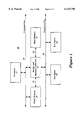
FIG. 1 illustrates a computer system which comprises a processor, a cache memory, a main memory, and a bridge and memory controller circuit;
FIG. 2 illustrates the bridge and memory controller of the computer system of FIG. 1 that includes a write buffer, a peripheral read prefetch buffer, and a peripheral write buffer along with a state machine that controls snoop ahead transactions;
FIG. 3 illustrates a write transaction targeted for the main memory that originates over the peripheral bus wherein the write transaction comprises an address phase followed by a series of data phases of line 0 data through line n data;
FIG. 4 illustrates the format of data stored in the peripheral write buffer including a set of double word data values each with a corresponding snoop status flag;
FIG. 5 illustrates a read transaction from the main memory over the peripheral bus wherein the read transaction comprises an address phase, and a set of wait states, followed by a set of data phases comprising line 0 data through line n data.
FIG. 1 illustrates a computer system 10. The computer system 10 comprises a processor 12, a cache memory 14, a main memory 18, and a bridge and memory controller 16. In addition, the processor 12 contains an internal level one (L1) cache memory.
The processor 12 is coupled for communication over a processor bus 24. The cache memory 14 is also coupled to the processor bus 24 and functions as a level two (L2) cache memory for the processor 12. The main memory 18 is comprised of dynamic random access memory (DRAM) and functions as the main memory storage for the computer system 10.
The bridge and memory controller 16 functions as a memory controller for the main memory 18. In addition, the bridge and memory controller 16 functions as a cache controller for the cache memory 14. The bridge and memory controller 16 enables read and write access to the main memory 18 from the processor bus 24 as well as a peripheral bus 26.
The bridge and memory controller 16 also functions as a bus bridge between the processor bus 24 and the peripheral bus 26. The bridge and memory controller 16 enables transactions originating on the processor bus 24 to propagate to the peripheral bus 26. In addition, the bridge and memory controller 16 enables transactions originating on the peripheral bus 26 from one of a set of bus agents 20 and 22 to propagate to the processor bus 24.
The bridge and memory controller 16 also enables the bus agents 20 and 22 to access data stored in the main memory 18 across bus 32. The bridge and memory controller 16 coordinates accesses to the main memory 18 across interface 32 that originate on the peripheral bus 26 with accesses to the main memory 18 that originate on the processor bus 24. In addition, the bridge and memory controller 16 initiates snoop request transactions on the processor bus 24 during memory accesses to the main memory 18 from the peripheral bus 26 in order to maintain cache coherency among the caches coupled to the processor bus 24. The caches coupled to the processor bus 24 include the internal L1 cache in the processor 12 along with the L2 cache memory 14 which is also coupled to bridge and memory controller 16.
FIG. 2 illustrates the bridge and memory controller 16 for one. The bridge and memory controller 16 includes a write buffer 42, a peripheral read prefetch buffer 44, and a peripheral write buffer 46. In addition, the bridge and memory controller 16 includes a state machine 40 that coordinates data transfers between the main memory 18 and the bus agents 20 and 22 via the peripheral bus 26, and that initiates snoop request transactions to the cache memories on the processor bus 24.
The write buffer 42 buffers write data targeted for the main memory 18 that originates from agents coupled to the processor bus 24 and agents coupled to the peripheral bus 26. A multiplexer 48 controlled by the state machine 40 selects either a data path from the processor bus 24 or a data path from the peripheral bus 26. The write buffer 42 compensates for the latency of DRAM accesses via a DRAM write path 52 in comparison to the speed of data transfer via the processor bus 24 or the peripheral bus 26.
The peripheral write buffer 46 buffers write data targeted for the main memory 18 that originates from bus agents on the peripheral bus 26. The peripheral write buffer 46 stores write data along with flags that are maintained by the state machine 40. The flags maintained by the state machine 40 indicate whether the data stored in the peripheral write buffer 46 corresponds to data lines having a completed snoop request transaction over the processor bus 24. The state machine 40 merges the data from the peripheral write buffer 46 into the write buffer 42 through the multiplexer 48 only after the corresponding snoop request transaction for the data line is complete over the processor bus 24.
The peripheral read prefetch buffer 44 prefetches sequential data lines from the main memory 18 in preparation for read transactions on the peripheral bus 26. The state machine 40 controls prefetches into the peripheral read prefetch buffer 44 to ensure that a read to the main memory 18 via a read path 54 does not occur until after the snoop transaction for the corresponding data line is completed via the processor bus 24.
FIG. 3 illustrates a write transaction targeted for the main memory 18 that originates over the peripheral bus 26. As shown, the write transaction comprises an address phase followed by a series of data phases comprising line 0 data through line n data. During the address phase, the peripheral bus 26 carries the address of data line 0 for the write transaction. Subsequently, the phases for the line 0 data through line n data each transfer an amount of data via the peripheral bus 26 equal to a cache line in the cache memory 14 or the internal cache of the processor 12.
To enable high bandwidth write transactions to the main memory 18 from the peripheral bus 26, the state machine 40 performs a snoop ahead transaction for each data line in the write transaction. For example, during the address phase of the write transaction on the peripheral bus 26, the state machine 40 issues a line 0 snoop request over the processor bus 24. Thereafter, the cache memory 14 and the internal cache of the processor 12 each perform either a writeback operation, also known as a copyback transaction, or an internal invalidate cache line operation depending upon the clean or dirty status of the cache line specified by the line 0 snoop request.
Thereafter, during the line 0 data phase of the write transaction on the peripheral bus 26, the line 0 snoop transaction on the processor bus 24 completes. As a consequence, the line 0 data buffered in the peripheral write buffer 46 is marked by the state machine 40 with a snoop done (SD) flag. Initially, the state machine 40 stores a snoop not done (SND) flag for the line 0 data contained in the peripheral write buffer 46 prior to the completion of the line 0 snoop request on the processor bus 24.
Later during the line 0 data phase, the state machine 40 generates a next sequential address corresponding to the line 1 data. Thereafter, the state machine 40 issues a line 1 snoop request over the processor bus 24. As shown, the state machine 40 continuously issues snoop request transactions over the processor bus 24 prior to the reception of the corresponding data line over the peripheral bus 26 during the write transaction. The snoop ahead transactions performed by the state machine 40 prevent the occurrence of wait cycles or delay cycles on the peripheral bus 26 during write transactions targeted for the main memory 18 through the peripheral write buffer 46.
FIG. 4 illustrates the format of data stored in the peripheral write buffer 46 for one embodiment. The peripheral write buffer 46 stores a set of double word data values each with a corresponding snoop status flag. The snoop status flag indicates either snoop done (SD) or snoop not done (SND) depending upon the status of the corresponding snoop ahead request issued by the state machine 40 over the processor bus 24. The boundary in the peripheral write buffer 46 between data having an SD indication and data having an SND indication provides a snoop boundary between line n-1 and line n. The state machine 40 merges the data from the peripheral write buffer 46 into the write buffer 42 only if the corresponding snoop status flag indicates snoop done.
FIG. 5 illustrates a read transaction from the main memory 18 over the peripheral bus 26. The read transaction on the peripheral bus 26 comprises an address phase, and a set of wait states, followed by a set of data phases comprising line 0 data through line n data. During the address phase of a read transaction, the originating bus agent on the peripheral bus 26 transfers the address of the initial data line being read from the main memory 18. As shown during the address phase, the state machine 40 issues a line 0 snoop request over the processor bus 24 that specifies the data line address provided during the address phase.
During the wait states on the peripheral bus 26, the line 0 snoop transaction on the processor bus 24 completes. Thereafter, a DRAM latency occurs while the peripheral read prefetch buffer 44 receives the corresponding data line from the main memory 18 via the read path 54. The line 0 prefetch to the peripheral read prefetch buffer 44 completes before the start of the line 0 data phase on the peripheral bus 26.
During the line 0 data phase on the peripheral bus 26, the peripheral read prefetch buffer 44 transfers the buffered read data over the peripheral bus 26 while the state machine 40 issues a line 1 snoop request over the processor bus 24 using an address generated as a next sequential cache line address from the address specified during the preceding address phase. Later in the line 0 data phase of the read transaction on the peripheral bus 26, the line 1 snoop transaction on the processor bus 24 completes. The completion of the line 1 snoop request enables a prefetch of the corresponding data line from the main memory 18 into the peripheral read prefetch buffer 44. Thereafter, the line 1 data from the peripheral read prefetch buffer 44 is transferred over the peripheral bus 26.
In addition, the state machine 40 monitors the occurrence of wait states on the peripheral bus 26 during read and write transactions. The state machine 40 counts the number of wait states that occur on the peripheral bus 26. The state machine 40 implements a disconnect time-out mechanism such that a disconnect is signaled over the peripheral bus 26 if the number of consecutive wait states on the peripheral bus 26 exceeds eight. The eight wait states conforms to the peripheral component interface (PCI) specification for maximum latency during data transfers. The disconnect indication on the peripheral bus 26 causes the bus agent that initiated the read transaction or the write transaction to terminate the transaction and try again later.
In the foregoing specification the invention has been described with reference to specific exemplary embodiments thereof. It will, however, be evident that various modifications and changes may be made thereto without departing from the broader spirit and scope of the invention as set forth in the appended claims. The specification and drawings are accordingly to be regarded as illustrative rather than a restrictive sense.
Claims (14)
1. A computer system, comprising:
a processor and a cache memory each coupled to a first bus;
a main memory;
a bus agent coupled to a second bus; and
a bus bridge and memory controller circuit coupled to the first bus and the second bus, the bus bridge and memory controller circuit including
a state machine to enable read and write access to the main memory from the first bus and the second bus and to perform a plurality of snoop ahead transactions to the cache memory over the first bus during corresponding memory access transactions originated by the bus agent over the second bus and targeted for the main memory, and
a buffer to store flags maintained by the state machine, the flags to indicate whether data stored in the buffer corresponds to data having a completed snoop ahead transaction over the first bus.
2. The computer system of claim 1, wherein the bus bridge and memory controller circuit further includes (i) a write buffer, coupled to the main memory, to buffer write data targeted for the main memory, and (ii) a multiplexer controlled by the state machine, to selectively merge write data received over the first bus with write data received over the second bus.
3. The computer system of claim 2, wherein the bus bridge and memory controller circuit further includes a peripheral write buffer, coupled to the multiplexer to buffer the write data received over the second bus.
4. The computer system of claim 2, wherein the bus bridge and memory controller circuit further includes a peripheral read prefetch buffer, coupled to the second bus, to prefetch read data from the main memory corresponding to the memory access transactions originated over the second bus only after a snoop ahead transaction of the plurality of snoop ahead transactions for the read data has completed.
5. A bus bridge and memory controller circuit for use in a computer system having a processor and a cache memory, each coupled to a first bus, and a bus agent coupled to a second bus, the bus bridge and memory controller circuit coupled to the first bus and the second bus, the computer system further including a main memory coupled to the bus bridge and memory controller circuit, the bus bridge and memory controller circuit comprising:
a state machine to enable read and write access to the main memory from the first bus and the second bus and to perform a plurality of snoop ahead transactions to the cache memory over the first bus during corresponding memory access transactions originated over the second bus and targeted for the main memory; and
a buffer to store flags maintained by the state machine indicating whether data stored in the buffer corresponds to data having a completed snoop ahead transaction over the first bus.
6. The bus bridge and memory controller circuit of claim 5, further including a peripheral read prefetch buffer coupled to the second bus, the peripheral read prefetch buffer prefetching read data from the main memory corresponding to the memory access transactions originated on the second bus only after a corresponding one of the plurality of snoop ahead transactions for the read data is complete.
7. The bus bridge and memory controller circuit of claim 5 further comprising a multiplexer coupled to the state machine.
8. The bus bridge and memory controller circuit of claim 7, wherein the multiplexer and the buffer are controlled by the state machine for merging of write data received over the first bus with write data received over the second bus.
9. Implemented within a computer system including a main memory, a cache memory, a first bus and a second bus, a bus bridge and memory controller circuit comprising:
first means for enabling a write access from the second bus to the main memory and for performing a plurality of snoop ahead transactions to the cache memory over the first bus during corresponding memory access transactions originated over the second bus and targeted for the main memory; and
second means for storing flags maintained by the first means indicating whether data stored in the second means corresponds to data having a completed snoop ahead transaction over the first bus.
10. The bus bridge and memory controller circuit of claim 9, wherein the first means includes a state machine.
11. The bus bridge and memory controller circuit of claim 9, wherein the second means includes a buffer.
12. The bus bridge and memory controller circuit of claim 9, wherein the first bus is a processor bus.
13. The bus bridge and memory controller circuit of claim 12, wherein the second bus is a peripheral bus.
14. The bus bridge and memory controller circuit of claim 13, wherein the peripheral bus is a Peripheral Component Interconnect (PCI) bus.
Priority Applications (1)
| Application Number | Priority Date | Filing Date | Title |
|---|---|---|---|
| US08/806,524 US6115796A (en) | 1995-01-20 | 1997-02-24 | Integrated bus bridge and memory controller that enables data streaming to a shared memory of a computer system using snoop ahead transactions |
Applications Claiming Priority (2)
| Application Number | Priority Date | Filing Date | Title |
|---|---|---|---|
| US08/375,972 US5630094A (en) | 1995-01-20 | 1995-01-20 | Integrated bus bridge and memory controller that enables data streaming to a shared memory of a computer system using snoop ahead transactions |
| US08/806,524 US6115796A (en) | 1995-01-20 | 1997-02-24 | Integrated bus bridge and memory controller that enables data streaming to a shared memory of a computer system using snoop ahead transactions |
Related Parent Applications (1)
| Application Number | Title | Priority Date | Filing Date |
|---|---|---|---|
| US08/375,972 Continuation US5630094A (en) | 1995-01-20 | 1995-01-20 | Integrated bus bridge and memory controller that enables data streaming to a shared memory of a computer system using snoop ahead transactions |
Publications (1)
| Publication Number | Publication Date |
|---|---|
| US6115796A true US6115796A (en) | 2000-09-05 |
Family
ID=23483143
Family Applications (2)
| Application Number | Title | Priority Date | Filing Date |
|---|---|---|---|
| US08/375,972 Expired - Lifetime US5630094A (en) | 1995-01-20 | 1995-01-20 | Integrated bus bridge and memory controller that enables data streaming to a shared memory of a computer system using snoop ahead transactions |
| US08/806,524 Expired - Lifetime US6115796A (en) | 1995-01-20 | 1997-02-24 | Integrated bus bridge and memory controller that enables data streaming to a shared memory of a computer system using snoop ahead transactions |
Family Applications Before (1)
| Application Number | Title | Priority Date | Filing Date |
|---|---|---|---|
| US08/375,972 Expired - Lifetime US5630094A (en) | 1995-01-20 | 1995-01-20 | Integrated bus bridge and memory controller that enables data streaming to a shared memory of a computer system using snoop ahead transactions |
Country Status (6)
| Country | Link |
|---|---|
| US (2) | US5630094A (en) |
| EP (1) | EP0804763B1 (en) |
| AU (1) | AU4699396A (en) |
| DE (1) | DE69604564T2 (en) |
| HK (1) | HK1004432A1 (en) |
| WO (1) | WO1996022571A1 (en) |
Cited By (9)
| Publication number | Priority date | Publication date | Assignee | Title |
|---|---|---|---|---|
| US6523093B1 (en) * | 2000-09-29 | 2003-02-18 | Intel Corporation | Prefetch buffer allocation and filtering system |
| US20030065843A1 (en) * | 2001-09-28 | 2003-04-03 | Jones Phillip M. | Next snoop predictor in a host controller |
| US6604162B1 (en) | 2000-06-28 | 2003-08-05 | Intel Corporation | Snoop stall reduction on a microprocessor external bus |
| US6748463B1 (en) * | 1996-03-13 | 2004-06-08 | Hitachi, Ltd. | Information processor with snoop suppressing function, memory controller, and direct memory access processing method |
| US20040199728A1 (en) * | 2003-04-07 | 2004-10-07 | Walker William J. | Methods and apparatus used to retrieve data from memory into a RAM controller before such data is requested |
| US6934770B1 (en) * | 2003-05-01 | 2005-08-23 | Adaptec, Inc. | Method for aborting data transfer commands |
| US20060031635A1 (en) * | 2004-08-09 | 2006-02-09 | Ofir Zohar | System method and circuit for retrieving into cache data from one or more mass data storage devices |
| US20080151765A1 (en) * | 2006-12-20 | 2008-06-26 | Sanal Chandran Cheruvathery | Enhanced Jitter Buffer |
| US20090106498A1 (en) * | 2007-10-23 | 2009-04-23 | Kevin Michael Lepak | Coherent dram prefetcher |
Families Citing this family (40)
| Publication number | Priority date | Publication date | Assignee | Title |
|---|---|---|---|---|
| US6002720A (en) * | 1991-01-07 | 1999-12-14 | H. Lee Browne, D/B/A Greenwich Information Technologies Llc | Audio and video transmission and receiving system |
| US5253275A (en) | 1991-01-07 | 1993-10-12 | H. Lee Browne | Audio and video transmission and receiving system |
| US5832241A (en) * | 1995-02-23 | 1998-11-03 | Intel Corporation | Data consistency across a bus transactions that impose ordering constraints |
| US5710906A (en) * | 1995-07-07 | 1998-01-20 | Opti Inc. | Predictive snooping of cache memory for master-initiated accesses |
| US5859988A (en) * | 1995-09-29 | 1999-01-12 | Intel Corporation | Triple-port bus bridge |
| US5712986A (en) * | 1995-12-19 | 1998-01-27 | Ncr Corporation | Asynchronous PCI-to-PCI Bridge |
| US5717876A (en) * | 1996-02-26 | 1998-02-10 | International Business Machines Corporation | Method for avoiding livelock on bus bridge receiving multiple requests |
| US5724613A (en) * | 1996-05-06 | 1998-03-03 | Vlsi Technology, Inc. | System and method for automatically enabling and disabling a prefetching capability |
| US5920891A (en) * | 1996-05-20 | 1999-07-06 | Advanced Micro Devices, Inc. | Architecture and method for controlling a cache memory |
| US6075929A (en) * | 1996-06-05 | 2000-06-13 | Compaq Computer Corporation | Prefetching data in response to a read transaction for which the requesting device relinquishes control of the data bus while awaiting data requested in the transaction |
| US5987539A (en) * | 1996-06-05 | 1999-11-16 | Compaq Computer Corporation | Method and apparatus for flushing a bridge device read buffer |
| US6035362A (en) * | 1996-06-05 | 2000-03-07 | Goodrum; Alan L. | Storing data associated with one request while continuing to store data associated with a previous request from the same device |
| US5872941A (en) * | 1996-06-05 | 1999-02-16 | Compaq Computer Corp. | Providing data from a bridge to a requesting device while the bridge is receiving the data |
| US5903906A (en) * | 1996-06-05 | 1999-05-11 | Compaq Computer Corporation | Receiving a write request that allows less than one cache line of data to be written and issuing a subsequent write request that requires at least one cache line of data to be written |
| US6052513A (en) * | 1996-06-05 | 2000-04-18 | Compaq Computer Corporation | Multi-threaded bus master |
| US6108741A (en) * | 1996-06-05 | 2000-08-22 | Maclaren; John M. | Ordering transactions |
| US6055590A (en) * | 1996-06-05 | 2000-04-25 | Compaq Computer Corporation | Bridge circuit comprising independent transaction buffers with control logic adapted to store overflow data in second buffer when transaction size exceeds the first buffer size |
| US5872939A (en) * | 1996-06-05 | 1999-02-16 | Compaq Computer Corporation | Bus arbitration |
| US6021480A (en) * | 1996-06-05 | 2000-02-01 | Compaq Computer Corporation | Aligning a memory read request with a cache line boundary when the request is for data beginning at a location in the middle of the cache line |
| US5768545A (en) * | 1996-06-11 | 1998-06-16 | Intel Corporation | Collect all transfers buffering mechanism utilizing passive release for a multiple bus environment |
| US5815675A (en) * | 1996-06-13 | 1998-09-29 | Vlsi Technology, Inc. | Method and apparatus for direct access to main memory by an I/O bus |
| US6021473A (en) * | 1996-08-27 | 2000-02-01 | Vlsi Technology, Inc. | Method and apparatus for maintaining coherency for data transaction of CPU and bus device utilizing selective flushing mechanism |
| KR100200968B1 (en) * | 1996-10-17 | 1999-06-15 | 윤종용 | Host interface circuit of image making apparatus |
| US5832245A (en) * | 1996-10-21 | 1998-11-03 | Advanced Micro Devices, Inc. | Method for isochronous flow control across an inter-chip bus |
| US5991819A (en) * | 1996-12-03 | 1999-11-23 | Intel Corporation | Dual-ported memory controller which maintains cache coherency using a memory line status table |
| US5835741A (en) * | 1996-12-31 | 1998-11-10 | Compaq Computer Corporation | Bus-to-bus bridge in computer system, with fast burst memory range |
| US6138192A (en) * | 1996-12-31 | 2000-10-24 | Compaq Computer Corporation | Delivering a request to write or read data before delivering an earlier write request |
| US5974511A (en) * | 1997-03-31 | 1999-10-26 | Sun Microsystems, Inc. | Cache subsystem with pseudo-packet switch |
| US5857082A (en) * | 1997-04-25 | 1999-01-05 | Intel Corporation | Method and apparatus for quickly transferring data from a first bus to a second bus |
| US5935233A (en) * | 1997-05-21 | 1999-08-10 | Micron Electronics, Inc. | Computer system with a switch interconnector for computer devices |
| US5931933A (en) * | 1997-06-16 | 1999-08-03 | International Business Machines Corporation | Apparatus and method for communication and translation for selected one of a variety of data bus formats |
| EP0924620A3 (en) * | 1997-12-22 | 2000-06-28 | Compaq Computer Corporation | Computer system including a bus bridge implementing adaptive speculative read operations |
| US6157398A (en) * | 1997-12-30 | 2000-12-05 | Micron Technology, Inc. | Method of implementing an accelerated graphics port for a multiple memory controller computer system |
| US7071946B2 (en) * | 1997-12-30 | 2006-07-04 | Micron Technology, Inc. | Accelerated graphics port for a multiple memory controller computer system |
| US6321307B1 (en) * | 1997-12-31 | 2001-11-20 | Compaq Computer Corporation | Computer system and method employing speculative snooping for optimizing performance |
| US6003106A (en) * | 1998-05-27 | 1999-12-14 | International Business Machines Corporation | DMA cache control logic |
| US6275885B1 (en) * | 1998-09-30 | 2001-08-14 | Compaq Computer Corp. | System and method for maintaining ownership of a processor bus while sending a programmed number of snoop cycles to the processor cache |
| US6434649B1 (en) * | 1998-10-14 | 2002-08-13 | Hitachi, Ltd. | Data streamer |
| US6385703B1 (en) * | 1998-12-03 | 2002-05-07 | Intel Corporation | Speculative request pointer advance for fast back-to-back reads |
| US7107383B1 (en) * | 2000-05-03 | 2006-09-12 | Broadcom Corporation | Method and system for multi-channel transfer of data and control information |
Citations (18)
| Publication number | Priority date | Publication date | Assignee | Title |
|---|---|---|---|---|
| EP0261029A2 (en) * | 1986-09-18 | 1988-03-23 | Digital Equipment Corporation | Cache invalidate protocol for digital data processing system |
| EP0288649A1 (en) * | 1987-04-22 | 1988-11-02 | International Business Machines Corporation | Memory control subsystem |
| US5072369A (en) * | 1989-04-07 | 1991-12-10 | Tektronix, Inc. | Interface between buses attached with cached modules providing address space mapped cache coherent memory access with SNOOP hit memory updates |
| US5195089A (en) * | 1990-12-31 | 1993-03-16 | Sun Microsystems, Inc. | Apparatus and method for a synchronous, high speed, packet-switched bus |
| JPH0637768A (en) * | 1992-07-17 | 1994-02-10 | Hitachi Ltd | Bus bridge for information processing unit |
| US5317718A (en) * | 1990-03-27 | 1994-05-31 | Digital Equipment Corporation | Data processing system and method with prefetch buffers |
| US5325503A (en) * | 1992-02-21 | 1994-06-28 | Compaq Computer Corporation | Cache memory system which snoops an operation to a first location in a cache line and does not snoop further operations to locations in the same line |
| US5335335A (en) * | 1991-08-30 | 1994-08-02 | Compaq Computer Corporation | Multiprocessor cache snoop access protocol wherein snoop means performs snooping operations after host bus cycle completion and delays subsequent host bus cycles until snooping operations are completed |
| US5341487A (en) * | 1991-12-20 | 1994-08-23 | International Business Machines Corp. | Personal computer having memory system with write-through cache and pipelined snoop cycles |
| US5353415A (en) * | 1992-10-02 | 1994-10-04 | Compaq Computer Corporation | Method and apparatus for concurrency of bus operations |
| US5355467A (en) * | 1991-06-04 | 1994-10-11 | Intel Corporation | Second level cache controller unit and system |
| US5359723A (en) * | 1991-12-16 | 1994-10-25 | Intel Corporation | Cache memory hierarchy having a large write through first level that allocates for CPU read misses only and a small write back second level that allocates for CPU write misses only |
| US5379384A (en) * | 1992-06-05 | 1995-01-03 | Intel Corporation | Configuration data loopback in a bus bridge circuit |
| US5420991A (en) * | 1994-01-04 | 1995-05-30 | Intel Corporation | Apparatus and method for maintaining processing consistency in a computer system having multiple processors |
| US5499355A (en) * | 1992-03-06 | 1996-03-12 | Rambus, Inc. | Prefetching into a cache to minimize main memory access time and cache size in a computer system |
| US5511226A (en) * | 1992-08-25 | 1996-04-23 | Intel Corporation | System for generating snoop addresses and conditionally generating source addresses whenever there is no snoop hit, the source addresses lagging behind the corresponding snoop addresses |
| US5572703A (en) * | 1994-03-01 | 1996-11-05 | Intel Corporation | Method and apparatus for snoop stretching using signals that convey snoop results |
| US5572702A (en) * | 1994-02-28 | 1996-11-05 | Intel Corporation | Method and apparatus for supporting read, write, and invalidation operations to memory which maintain cache consistency |
-
1995
- 1995-01-20 US US08/375,972 patent/US5630094A/en not_active Expired - Lifetime
-
1996
- 1996-01-16 WO PCT/US1996/000506 patent/WO1996022571A1/en active IP Right Grant
- 1996-01-16 DE DE69604564T patent/DE69604564T2/en not_active Expired - Lifetime
- 1996-01-16 AU AU46993/96A patent/AU4699396A/en not_active Abandoned
- 1996-01-16 EP EP96902679A patent/EP0804763B1/en not_active Expired - Lifetime
-
1997
- 1997-02-24 US US08/806,524 patent/US6115796A/en not_active Expired - Lifetime
-
1998
- 1998-05-04 HK HK98103810A patent/HK1004432A1/en not_active IP Right Cessation
Patent Citations (18)
| Publication number | Priority date | Publication date | Assignee | Title |
|---|---|---|---|---|
| EP0261029A2 (en) * | 1986-09-18 | 1988-03-23 | Digital Equipment Corporation | Cache invalidate protocol for digital data processing system |
| EP0288649A1 (en) * | 1987-04-22 | 1988-11-02 | International Business Machines Corporation | Memory control subsystem |
| US5072369A (en) * | 1989-04-07 | 1991-12-10 | Tektronix, Inc. | Interface between buses attached with cached modules providing address space mapped cache coherent memory access with SNOOP hit memory updates |
| US5317718A (en) * | 1990-03-27 | 1994-05-31 | Digital Equipment Corporation | Data processing system and method with prefetch buffers |
| US5195089A (en) * | 1990-12-31 | 1993-03-16 | Sun Microsystems, Inc. | Apparatus and method for a synchronous, high speed, packet-switched bus |
| US5355467A (en) * | 1991-06-04 | 1994-10-11 | Intel Corporation | Second level cache controller unit and system |
| US5335335A (en) * | 1991-08-30 | 1994-08-02 | Compaq Computer Corporation | Multiprocessor cache snoop access protocol wherein snoop means performs snooping operations after host bus cycle completion and delays subsequent host bus cycles until snooping operations are completed |
| US5359723A (en) * | 1991-12-16 | 1994-10-25 | Intel Corporation | Cache memory hierarchy having a large write through first level that allocates for CPU read misses only and a small write back second level that allocates for CPU write misses only |
| US5341487A (en) * | 1991-12-20 | 1994-08-23 | International Business Machines Corp. | Personal computer having memory system with write-through cache and pipelined snoop cycles |
| US5325503A (en) * | 1992-02-21 | 1994-06-28 | Compaq Computer Corporation | Cache memory system which snoops an operation to a first location in a cache line and does not snoop further operations to locations in the same line |
| US5499355A (en) * | 1992-03-06 | 1996-03-12 | Rambus, Inc. | Prefetching into a cache to minimize main memory access time and cache size in a computer system |
| US5379384A (en) * | 1992-06-05 | 1995-01-03 | Intel Corporation | Configuration data loopback in a bus bridge circuit |
| JPH0637768A (en) * | 1992-07-17 | 1994-02-10 | Hitachi Ltd | Bus bridge for information processing unit |
| US5511226A (en) * | 1992-08-25 | 1996-04-23 | Intel Corporation | System for generating snoop addresses and conditionally generating source addresses whenever there is no snoop hit, the source addresses lagging behind the corresponding snoop addresses |
| US5353415A (en) * | 1992-10-02 | 1994-10-04 | Compaq Computer Corporation | Method and apparatus for concurrency of bus operations |
| US5420991A (en) * | 1994-01-04 | 1995-05-30 | Intel Corporation | Apparatus and method for maintaining processing consistency in a computer system having multiple processors |
| US5572702A (en) * | 1994-02-28 | 1996-11-05 | Intel Corporation | Method and apparatus for supporting read, write, and invalidation operations to memory which maintain cache consistency |
| US5572703A (en) * | 1994-03-01 | 1996-11-05 | Intel Corporation | Method and apparatus for snoop stretching using signals that convey snoop results |
Non-Patent Citations (2)
| Title |
|---|
| "Micro Channel Data Streaming and Input/Output Snooping Facility for Personal Computer Systems", IBM Technical Disclosure Bulletin, vol 36, No. 10, Oct., 1993, pp. 187-191. |
| Micro Channel Data Streaming and Input/Output Snooping Facility for Personal Computer Systems , IBM Technical Disclosure Bulletin, vol 36, No. 10, Oct., 1993, pp. 187 191. * |
Cited By (12)
| Publication number | Priority date | Publication date | Assignee | Title |
|---|---|---|---|---|
| US6748463B1 (en) * | 1996-03-13 | 2004-06-08 | Hitachi, Ltd. | Information processor with snoop suppressing function, memory controller, and direct memory access processing method |
| US6604162B1 (en) | 2000-06-28 | 2003-08-05 | Intel Corporation | Snoop stall reduction on a microprocessor external bus |
| US6523093B1 (en) * | 2000-09-29 | 2003-02-18 | Intel Corporation | Prefetch buffer allocation and filtering system |
| US20030065843A1 (en) * | 2001-09-28 | 2003-04-03 | Jones Phillip M. | Next snoop predictor in a host controller |
| US6829665B2 (en) * | 2001-09-28 | 2004-12-07 | Hewlett-Packard Development Company, L.P. | Next snoop predictor in a host controller |
| US20040199728A1 (en) * | 2003-04-07 | 2004-10-07 | Walker William J. | Methods and apparatus used to retrieve data from memory into a RAM controller before such data is requested |
| US7055005B2 (en) * | 2003-04-07 | 2006-05-30 | Hewlett-Packard Development Company, L.P. | Methods and apparatus used to retrieve data from memory into a RAM controller before such data is requested |
| US6934770B1 (en) * | 2003-05-01 | 2005-08-23 | Adaptec, Inc. | Method for aborting data transfer commands |
| US20060031635A1 (en) * | 2004-08-09 | 2006-02-09 | Ofir Zohar | System method and circuit for retrieving into cache data from one or more mass data storage devices |
| US7430641B2 (en) * | 2004-08-09 | 2008-09-30 | Xiv Ltd. | System method and circuit for retrieving into cache data from one or more mass data storage devices |
| US20080151765A1 (en) * | 2006-12-20 | 2008-06-26 | Sanal Chandran Cheruvathery | Enhanced Jitter Buffer |
| US20090106498A1 (en) * | 2007-10-23 | 2009-04-23 | Kevin Michael Lepak | Coherent dram prefetcher |
Also Published As
| Publication number | Publication date |
|---|---|
| EP0804763A1 (en) | 1997-11-05 |
| EP0804763B1 (en) | 1999-10-06 |
| US5630094A (en) | 1997-05-13 |
| EP0804763A4 (en) | 1998-04-01 |
| DE69604564D1 (en) | 1999-11-11 |
| DE69604564T2 (en) | 2000-05-31 |
| AU4699396A (en) | 1996-08-07 |
| WO1996022571A1 (en) | 1996-07-25 |
| HK1004432A1 (en) | 1998-11-27 |
Similar Documents
| Publication | Publication Date | Title |
|---|---|---|
| US6115796A (en) | Integrated bus bridge and memory controller that enables data streaming to a shared memory of a computer system using snoop ahead transactions | |
| US5353415A (en) | Method and apparatus for concurrency of bus operations | |
| US5463753A (en) | Method and apparatus for reducing non-snoop window of a cache controller by delaying host bus grant signal to the cache controller | |
| US6405271B1 (en) | Data flow control mechanism for a bus supporting two-and three-agent transactions | |
| US6434639B1 (en) | System for combining requests associated with one or more memory locations that are collectively associated with a single cache line to furnish a single memory operation | |
| US6279087B1 (en) | System and method for maintaining coherency and improving performance in a bus bridge supporting write posting operations | |
| US6199131B1 (en) | Computer system employing optimized delayed transaction arbitration technique | |
| US5664150A (en) | Computer system with a device for selectively blocking writebacks of data from a writeback cache to memory | |
| US5499353A (en) | Cache address strobe control logic for stimulated bus cycle initiation | |
| US6321296B1 (en) | SDRAM L3 cache using speculative loads with command aborts to lower latency | |
| US6718441B2 (en) | Method to prefetch data from system memory using a bus interface unit | |
| GB2287110A (en) | Method and apparatus for snoop stretching | |
| US20030135670A1 (en) | DMA controller and coherency-tracking unit for efficient data transfers between coherent and non-coherentmemory spaces | |
| US20020087803A1 (en) | Apparatus for identifying memory requests originating on remote I/O devices as noncacheable | |
| WO1994008297A9 (en) | Method and apparatus for concurrency of bus operations | |
| US11500797B2 (en) | Computer memory expansion device and method of operation | |
| US5479636A (en) | Concurrent cache line replacement method and apparatus in microprocessor system with write-back cache memory | |
| US5918069A (en) | System for simultaneously writing back cached data via first bus and transferring cached data to second bus when read request is cached and dirty | |
| US6321307B1 (en) | Computer system and method employing speculative snooping for optimizing performance | |
| US6321302B1 (en) | Stream read buffer for efficient interface with block oriented devices | |
| US5353429A (en) | Cache memory systems that accesses main memory without wait states during cache misses, using a state machine and address latch in the memory controller | |
| JP2001147854A (en) | Processing system and method for optimizing storage in writing buffer unit and method for storing and distributing data | |
| US5974497A (en) | Computer with cache-line buffers for storing prefetched data for a misaligned memory access | |
| US5987570A (en) | Performing overlapping burst memory accesses and interleaved memory accesses on cache misses | |
| JPH0271344A (en) | Micro-computer-system |
Legal Events
| Date | Code | Title | Description |
|---|---|---|---|
| STCF | Information on status: patent grant |
Free format text: PATENTED CASE |
|
| CC | Certificate of correction | ||
| FEPP | Fee payment procedure |
Free format text: PAYOR NUMBER ASSIGNED (ORIGINAL EVENT CODE: ASPN); ENTITY STATUS OF PATENT OWNER: LARGE ENTITY |
|
| FPAY | Fee payment |
Year of fee payment: 4 |
|
| FEPP | Fee payment procedure |
Free format text: PAYOR NUMBER ASSIGNED (ORIGINAL EVENT CODE: ASPN); ENTITY STATUS OF PATENT OWNER: LARGE ENTITY |
|
| FPAY | Fee payment |
Year of fee payment: 8 |
|
| FPAY | Fee payment |
Year of fee payment: 12 |