US6117734A - Method of forming a trench MOS gate on a power semiconductor device - Google Patents
Method of forming a trench MOS gate on a power semiconductor device Download PDFInfo
- Publication number
- US6117734A US6117734A US08/996,041 US99604197A US6117734A US 6117734 A US6117734 A US 6117734A US 99604197 A US99604197 A US 99604197A US 6117734 A US6117734 A US 6117734A
- Authority
- US
- United States
- Prior art keywords
- trench
- oxide film
- substrate
- gate
- etching
- Prior art date
- Legal status (The legal status is an assumption and is not a legal conclusion. Google has not performed a legal analysis and makes no representation as to the accuracy of the status listed.)
- Expired - Lifetime
Links
- 239000004065 semiconductor Substances 0.000 title claims abstract description 74
- 238000000034 method Methods 0.000 title claims description 63
- 238000004519 manufacturing process Methods 0.000 claims abstract description 21
- 239000000758 substrate Substances 0.000 claims description 87
- 238000005530 etching Methods 0.000 claims description 48
- 238000002955 isolation Methods 0.000 claims description 43
- 230000003647 oxidation Effects 0.000 claims description 42
- 238000007254 oxidation reaction Methods 0.000 claims description 42
- QVGXLLKOCUKJST-UHFFFAOYSA-N atomic oxygen Chemical compound [O] QVGXLLKOCUKJST-UHFFFAOYSA-N 0.000 claims description 20
- 239000001301 oxygen Substances 0.000 claims description 20
- 229910052760 oxygen Inorganic materials 0.000 claims description 20
- 230000001590 oxidative effect Effects 0.000 claims description 8
- 238000001312 dry etching Methods 0.000 claims description 7
- 239000000463 material Substances 0.000 claims description 7
- VYPSYNLAJGMNEJ-UHFFFAOYSA-N Silicium dioxide Chemical compound O=[Si]=O VYPSYNLAJGMNEJ-UHFFFAOYSA-N 0.000 abstract description 54
- 229910052814 silicon oxide Inorganic materials 0.000 abstract description 54
- 230000015572 biosynthetic process Effects 0.000 abstract description 15
- 230000007547 defect Effects 0.000 abstract description 14
- 230000005684 electric field Effects 0.000 abstract description 7
- 230000006872 improvement Effects 0.000 abstract description 3
- 239000000969 carrier Substances 0.000 abstract description 2
- 229910021420 polycrystalline silicon Inorganic materials 0.000 description 32
- 230000015556 catabolic process Effects 0.000 description 26
- XUIMIQQOPSSXEZ-UHFFFAOYSA-N Silicon Chemical compound [Si] XUIMIQQOPSSXEZ-UHFFFAOYSA-N 0.000 description 17
- 229910052710 silicon Inorganic materials 0.000 description 17
- 239000010703 silicon Substances 0.000 description 17
- 239000007789 gas Substances 0.000 description 11
- 230000008569 process Effects 0.000 description 10
- 230000000694 effects Effects 0.000 description 9
- 230000008021 deposition Effects 0.000 description 6
- 238000001020 plasma etching Methods 0.000 description 6
- 230000007423 decrease Effects 0.000 description 5
- 238000011109 contamination Methods 0.000 description 4
- 238000009499 grossing Methods 0.000 description 3
- 230000009467 reduction Effects 0.000 description 3
- 229910004012 SiCx Inorganic materials 0.000 description 2
- 150000001875 compounds Chemical class 0.000 description 2
- 238000010276 construction Methods 0.000 description 2
- 230000002950 deficient Effects 0.000 description 2
- 238000005247 gettering Methods 0.000 description 2
- 239000012212 insulator Substances 0.000 description 2
- 238000007493 shaping process Methods 0.000 description 2
- XLYOFNOQVPJJNP-UHFFFAOYSA-N water Substances O XLYOFNOQVPJJNP-UHFFFAOYSA-N 0.000 description 2
- 229910000789 Aluminium-silicon alloy Inorganic materials 0.000 description 1
- 229910020968 MoSi2 Inorganic materials 0.000 description 1
- 229910052581 Si3N4 Inorganic materials 0.000 description 1
- -1 SiCx (0<x<1) Chemical class 0.000 description 1
- 229910008484 TiSi Inorganic materials 0.000 description 1
- 229910008812 WSi Inorganic materials 0.000 description 1
- 238000000137 annealing Methods 0.000 description 1
- 230000003247 decreasing effect Effects 0.000 description 1
- 238000006073 displacement reaction Methods 0.000 description 1
- 238000009826 distribution Methods 0.000 description 1
- 230000002708 enhancing effect Effects 0.000 description 1
- 230000010354 integration Effects 0.000 description 1
- 239000002184 metal Substances 0.000 description 1
- 229910052751 metal Inorganic materials 0.000 description 1
- 230000004048 modification Effects 0.000 description 1
- 238000012986 modification Methods 0.000 description 1
- HQVNEWCFYHHQES-UHFFFAOYSA-N silicon nitride Chemical compound N12[Si]34N5[Si]62N3[Si]51N64 HQVNEWCFYHHQES-UHFFFAOYSA-N 0.000 description 1
- 238000005549 size reduction Methods 0.000 description 1
Images


Classifications
-
- H—ELECTRICITY
- H01—ELECTRIC ELEMENTS
- H01L—SEMICONDUCTOR DEVICES NOT COVERED BY CLASS H10
- H01L29/00—Semiconductor devices adapted for rectifying, amplifying, oscillating or switching, or capacitors or resistors with at least one potential-jump barrier or surface barrier, e.g. PN junction depletion layer or carrier concentration layer; Details of semiconductor bodies or of electrodes thereof ; Multistep manufacturing processes therefor
- H01L29/66—Types of semiconductor device ; Multistep manufacturing processes therefor
- H01L29/68—Types of semiconductor device ; Multistep manufacturing processes therefor controllable by only the electric current supplied, or only the electric potential applied, to an electrode which does not carry the current to be rectified, amplified or switched
- H01L29/76—Unipolar devices, e.g. field effect transistors
- H01L29/772—Field effect transistors
- H01L29/78—Field effect transistors with field effect produced by an insulated gate
- H01L29/7801—DMOS transistors, i.e. MISFETs with a channel accommodating body or base region adjoining a drain drift region
- H01L29/7816—Lateral DMOS transistors, i.e. LDMOS transistors
- H01L29/7824—Lateral DMOS transistors, i.e. LDMOS transistors with a substrate comprising an insulating layer, e.g. SOI-LDMOS transistors
-
- H—ELECTRICITY
- H01—ELECTRIC ELEMENTS
- H01L—SEMICONDUCTOR DEVICES NOT COVERED BY CLASS H10
- H01L21/00—Processes or apparatus adapted for the manufacture or treatment of semiconductor or solid state devices or of parts thereof
- H01L21/70—Manufacture or treatment of devices consisting of a plurality of solid state components formed in or on a common substrate or of parts thereof; Manufacture of integrated circuit devices or of parts thereof
- H01L21/71—Manufacture of specific parts of devices defined in group H01L21/70
- H01L21/76—Making of isolation regions between components
- H01L21/762—Dielectric regions, e.g. EPIC dielectric isolation, LOCOS; Trench refilling techniques, SOI technology, use of channel stoppers
- H01L21/76224—Dielectric regions, e.g. EPIC dielectric isolation, LOCOS; Trench refilling techniques, SOI technology, use of channel stoppers using trench refilling with dielectric materials
- H01L21/76232—Dielectric regions, e.g. EPIC dielectric isolation, LOCOS; Trench refilling techniques, SOI technology, use of channel stoppers using trench refilling with dielectric materials of trenches having a shape other than rectangular or V-shape, e.g. rounded corners, oblique or rounded trench walls
-
- H—ELECTRICITY
- H01—ELECTRIC ELEMENTS
- H01L—SEMICONDUCTOR DEVICES NOT COVERED BY CLASS H10
- H01L21/00—Processes or apparatus adapted for the manufacture or treatment of semiconductor or solid state devices or of parts thereof
- H01L21/70—Manufacture or treatment of devices consisting of a plurality of solid state components formed in or on a common substrate or of parts thereof; Manufacture of integrated circuit devices or of parts thereof
- H01L21/71—Manufacture of specific parts of devices defined in group H01L21/70
- H01L21/76—Making of isolation regions between components
- H01L21/762—Dielectric regions, e.g. EPIC dielectric isolation, LOCOS; Trench refilling techniques, SOI technology, use of channel stoppers
- H01L21/7624—Dielectric regions, e.g. EPIC dielectric isolation, LOCOS; Trench refilling techniques, SOI technology, use of channel stoppers using semiconductor on insulator [SOI] technology
- H01L21/76264—SOI together with lateral isolation, e.g. using local oxidation of silicon, or dielectric or polycristalline material refilled trench or air gap isolation regions, e.g. completely isolated semiconductor islands
-
- H—ELECTRICITY
- H01—ELECTRIC ELEMENTS
- H01L—SEMICONDUCTOR DEVICES NOT COVERED BY CLASS H10
- H01L21/00—Processes or apparatus adapted for the manufacture or treatment of semiconductor or solid state devices or of parts thereof
- H01L21/70—Manufacture or treatment of devices consisting of a plurality of solid state components formed in or on a common substrate or of parts thereof; Manufacture of integrated circuit devices or of parts thereof
- H01L21/71—Manufacture of specific parts of devices defined in group H01L21/70
- H01L21/76—Making of isolation regions between components
- H01L21/763—Polycrystalline semiconductor regions
-
- H—ELECTRICITY
- H01—ELECTRIC ELEMENTS
- H01L—SEMICONDUCTOR DEVICES NOT COVERED BY CLASS H10
- H01L29/00—Semiconductor devices adapted for rectifying, amplifying, oscillating or switching, or capacitors or resistors with at least one potential-jump barrier or surface barrier, e.g. PN junction depletion layer or carrier concentration layer; Details of semiconductor bodies or of electrodes thereof ; Multistep manufacturing processes therefor
- H01L29/02—Semiconductor bodies ; Multistep manufacturing processes therefor
- H01L29/06—Semiconductor bodies ; Multistep manufacturing processes therefor characterised by their shape; characterised by the shapes, relative sizes, or dispositions of the semiconductor regions ; characterised by the concentration or distribution of impurities within semiconductor regions
- H01L29/0684—Semiconductor bodies ; Multistep manufacturing processes therefor characterised by their shape; characterised by the shapes, relative sizes, or dispositions of the semiconductor regions ; characterised by the concentration or distribution of impurities within semiconductor regions characterised by the shape, relative sizes or dispositions of the semiconductor regions or junctions between the regions
- H01L29/0692—Surface layout
- H01L29/0696—Surface layout of cellular field-effect devices, e.g. multicellular DMOS transistors or IGBTs
-
- H—ELECTRICITY
- H01—ELECTRIC ELEMENTS
- H01L—SEMICONDUCTOR DEVICES NOT COVERED BY CLASS H10
- H01L29/00—Semiconductor devices adapted for rectifying, amplifying, oscillating or switching, or capacitors or resistors with at least one potential-jump barrier or surface barrier, e.g. PN junction depletion layer or carrier concentration layer; Details of semiconductor bodies or of electrodes thereof ; Multistep manufacturing processes therefor
- H01L29/40—Electrodes ; Multistep manufacturing processes therefor
- H01L29/41—Electrodes ; Multistep manufacturing processes therefor characterised by their shape, relative sizes or dispositions
- H01L29/423—Electrodes ; Multistep manufacturing processes therefor characterised by their shape, relative sizes or dispositions not carrying the current to be rectified, amplified or switched
- H01L29/42312—Gate electrodes for field effect devices
- H01L29/42316—Gate electrodes for field effect devices for field-effect transistors
- H01L29/4232—Gate electrodes for field effect devices for field-effect transistors with insulated gate
- H01L29/42356—Disposition, e.g. buried gate electrode
- H01L29/4236—Disposition, e.g. buried gate electrode within a trench, e.g. trench gate electrode, groove gate electrode
-
- H—ELECTRICITY
- H01—ELECTRIC ELEMENTS
- H01L—SEMICONDUCTOR DEVICES NOT COVERED BY CLASS H10
- H01L29/00—Semiconductor devices adapted for rectifying, amplifying, oscillating or switching, or capacitors or resistors with at least one potential-jump barrier or surface barrier, e.g. PN junction depletion layer or carrier concentration layer; Details of semiconductor bodies or of electrodes thereof ; Multistep manufacturing processes therefor
- H01L29/66—Types of semiconductor device ; Multistep manufacturing processes therefor
- H01L29/66007—Multistep manufacturing processes
- H01L29/66075—Multistep manufacturing processes of devices having semiconductor bodies comprising group 14 or group 13/15 materials
- H01L29/66227—Multistep manufacturing processes of devices having semiconductor bodies comprising group 14 or group 13/15 materials the devices being controllable only by the electric current supplied or the electric potential applied, to an electrode which does not carry the current to be rectified, amplified or switched, e.g. three-terminal devices
- H01L29/66234—Bipolar junction transistors [BJT]
- H01L29/66325—Bipolar junction transistors [BJT] controlled by field-effect, e.g. insulated gate bipolar transistors [IGBT]
- H01L29/66333—Vertical insulated gate bipolar transistors
- H01L29/66348—Vertical insulated gate bipolar transistors with a recessed gate
-
- H—ELECTRICITY
- H01—ELECTRIC ELEMENTS
- H01L—SEMICONDUCTOR DEVICES NOT COVERED BY CLASS H10
- H01L29/00—Semiconductor devices adapted for rectifying, amplifying, oscillating or switching, or capacitors or resistors with at least one potential-jump barrier or surface barrier, e.g. PN junction depletion layer or carrier concentration layer; Details of semiconductor bodies or of electrodes thereof ; Multistep manufacturing processes therefor
- H01L29/66—Types of semiconductor device ; Multistep manufacturing processes therefor
- H01L29/66007—Multistep manufacturing processes
- H01L29/66075—Multistep manufacturing processes of devices having semiconductor bodies comprising group 14 or group 13/15 materials
- H01L29/66227—Multistep manufacturing processes of devices having semiconductor bodies comprising group 14 or group 13/15 materials the devices being controllable only by the electric current supplied or the electric potential applied, to an electrode which does not carry the current to be rectified, amplified or switched, e.g. three-terminal devices
- H01L29/66356—Gated diodes, e.g. field controlled diodes [FCD], static induction thyristors [SITh], field controlled thyristors [FCTh]
-
- H—ELECTRICITY
- H01—ELECTRIC ELEMENTS
- H01L—SEMICONDUCTOR DEVICES NOT COVERED BY CLASS H10
- H01L29/00—Semiconductor devices adapted for rectifying, amplifying, oscillating or switching, or capacitors or resistors with at least one potential-jump barrier or surface barrier, e.g. PN junction depletion layer or carrier concentration layer; Details of semiconductor bodies or of electrodes thereof ; Multistep manufacturing processes therefor
- H01L29/66—Types of semiconductor device ; Multistep manufacturing processes therefor
- H01L29/66007—Multistep manufacturing processes
- H01L29/66075—Multistep manufacturing processes of devices having semiconductor bodies comprising group 14 or group 13/15 materials
- H01L29/66227—Multistep manufacturing processes of devices having semiconductor bodies comprising group 14 or group 13/15 materials the devices being controllable only by the electric current supplied or the electric potential applied, to an electrode which does not carry the current to be rectified, amplified or switched, e.g. three-terminal devices
- H01L29/66363—Thyristors
- H01L29/66371—Thyristors structurally associated with another device, e.g. built-in diode
- H01L29/66378—Thyristors structurally associated with another device, e.g. built-in diode the other device being a controlling field-effect device
-
- H—ELECTRICITY
- H01—ELECTRIC ELEMENTS
- H01L—SEMICONDUCTOR DEVICES NOT COVERED BY CLASS H10
- H01L29/00—Semiconductor devices adapted for rectifying, amplifying, oscillating or switching, or capacitors or resistors with at least one potential-jump barrier or surface barrier, e.g. PN junction depletion layer or carrier concentration layer; Details of semiconductor bodies or of electrodes thereof ; Multistep manufacturing processes therefor
- H01L29/66—Types of semiconductor device ; Multistep manufacturing processes therefor
- H01L29/66007—Multistep manufacturing processes
- H01L29/66075—Multistep manufacturing processes of devices having semiconductor bodies comprising group 14 or group 13/15 materials
- H01L29/66227—Multistep manufacturing processes of devices having semiconductor bodies comprising group 14 or group 13/15 materials the devices being controllable only by the electric current supplied or the electric potential applied, to an electrode which does not carry the current to be rectified, amplified or switched, e.g. three-terminal devices
- H01L29/66409—Unipolar field-effect transistors
- H01L29/66477—Unipolar field-effect transistors with an insulated gate, i.e. MISFET
- H01L29/66666—Vertical transistors
-
- H—ELECTRICITY
- H01—ELECTRIC ELEMENTS
- H01L—SEMICONDUCTOR DEVICES NOT COVERED BY CLASS H10
- H01L29/00—Semiconductor devices adapted for rectifying, amplifying, oscillating or switching, or capacitors or resistors with at least one potential-jump barrier or surface barrier, e.g. PN junction depletion layer or carrier concentration layer; Details of semiconductor bodies or of electrodes thereof ; Multistep manufacturing processes therefor
- H01L29/66—Types of semiconductor device ; Multistep manufacturing processes therefor
- H01L29/66007—Multistep manufacturing processes
- H01L29/66075—Multistep manufacturing processes of devices having semiconductor bodies comprising group 14 or group 13/15 materials
- H01L29/66227—Multistep manufacturing processes of devices having semiconductor bodies comprising group 14 or group 13/15 materials the devices being controllable only by the electric current supplied or the electric potential applied, to an electrode which does not carry the current to be rectified, amplified or switched, e.g. three-terminal devices
- H01L29/66409—Unipolar field-effect transistors
- H01L29/66477—Unipolar field-effect transistors with an insulated gate, i.e. MISFET
- H01L29/66674—DMOS transistors, i.e. MISFETs with a channel accommodating body or base region adjoining a drain drift region
- H01L29/66712—Vertical DMOS transistors, i.e. VDMOS transistors
- H01L29/66734—Vertical DMOS transistors, i.e. VDMOS transistors with a step of recessing the gate electrode, e.g. to form a trench gate electrode
-
- H—ELECTRICITY
- H01—ELECTRIC ELEMENTS
- H01L—SEMICONDUCTOR DEVICES NOT COVERED BY CLASS H10
- H01L29/00—Semiconductor devices adapted for rectifying, amplifying, oscillating or switching, or capacitors or resistors with at least one potential-jump barrier or surface barrier, e.g. PN junction depletion layer or carrier concentration layer; Details of semiconductor bodies or of electrodes thereof ; Multistep manufacturing processes therefor
- H01L29/66—Types of semiconductor device ; Multistep manufacturing processes therefor
- H01L29/68—Types of semiconductor device ; Multistep manufacturing processes therefor controllable by only the electric current supplied, or only the electric potential applied, to an electrode which does not carry the current to be rectified, amplified or switched
- H01L29/70—Bipolar devices
- H01L29/72—Transistor-type devices, i.e. able to continuously respond to applied control signals
- H01L29/739—Transistor-type devices, i.e. able to continuously respond to applied control signals controlled by field-effect, e.g. bipolar static induction transistors [BSIT]
- H01L29/7391—Gated diode structures
-
- H—ELECTRICITY
- H01—ELECTRIC ELEMENTS
- H01L—SEMICONDUCTOR DEVICES NOT COVERED BY CLASS H10
- H01L29/00—Semiconductor devices adapted for rectifying, amplifying, oscillating or switching, or capacitors or resistors with at least one potential-jump barrier or surface barrier, e.g. PN junction depletion layer or carrier concentration layer; Details of semiconductor bodies or of electrodes thereof ; Multistep manufacturing processes therefor
- H01L29/66—Types of semiconductor device ; Multistep manufacturing processes therefor
- H01L29/68—Types of semiconductor device ; Multistep manufacturing processes therefor controllable by only the electric current supplied, or only the electric potential applied, to an electrode which does not carry the current to be rectified, amplified or switched
- H01L29/70—Bipolar devices
- H01L29/72—Transistor-type devices, i.e. able to continuously respond to applied control signals
- H01L29/739—Transistor-type devices, i.e. able to continuously respond to applied control signals controlled by field-effect, e.g. bipolar static induction transistors [BSIT]
- H01L29/7393—Insulated gate bipolar mode transistors, i.e. IGBT; IGT; COMFET
- H01L29/7394—Insulated gate bipolar mode transistors, i.e. IGBT; IGT; COMFET on an insulating layer or substrate, e.g. thin film device or device isolated from the bulk substrate
-
- H—ELECTRICITY
- H01—ELECTRIC ELEMENTS
- H01L—SEMICONDUCTOR DEVICES NOT COVERED BY CLASS H10
- H01L29/00—Semiconductor devices adapted for rectifying, amplifying, oscillating or switching, or capacitors or resistors with at least one potential-jump barrier or surface barrier, e.g. PN junction depletion layer or carrier concentration layer; Details of semiconductor bodies or of electrodes thereof ; Multistep manufacturing processes therefor
- H01L29/66—Types of semiconductor device ; Multistep manufacturing processes therefor
- H01L29/68—Types of semiconductor device ; Multistep manufacturing processes therefor controllable by only the electric current supplied, or only the electric potential applied, to an electrode which does not carry the current to be rectified, amplified or switched
- H01L29/70—Bipolar devices
- H01L29/72—Transistor-type devices, i.e. able to continuously respond to applied control signals
- H01L29/739—Transistor-type devices, i.e. able to continuously respond to applied control signals controlled by field-effect, e.g. bipolar static induction transistors [BSIT]
- H01L29/7393—Insulated gate bipolar mode transistors, i.e. IGBT; IGT; COMFET
- H01L29/7395—Vertical transistors, e.g. vertical IGBT
- H01L29/7396—Vertical transistors, e.g. vertical IGBT with a non planar surface, e.g. with a non planar gate or with a trench or recess or pillar in the surface of the emitter, base or collector region for improving current density or short circuiting the emitter and base regions
- H01L29/7397—Vertical transistors, e.g. vertical IGBT with a non planar surface, e.g. with a non planar gate or with a trench or recess or pillar in the surface of the emitter, base or collector region for improving current density or short circuiting the emitter and base regions and a gate structure lying on a slanted or vertical surface or formed in a groove, e.g. trench gate IGBT
-
- H—ELECTRICITY
- H01—ELECTRIC ELEMENTS
- H01L—SEMICONDUCTOR DEVICES NOT COVERED BY CLASS H10
- H01L29/00—Semiconductor devices adapted for rectifying, amplifying, oscillating or switching, or capacitors or resistors with at least one potential-jump barrier or surface barrier, e.g. PN junction depletion layer or carrier concentration layer; Details of semiconductor bodies or of electrodes thereof ; Multistep manufacturing processes therefor
- H01L29/66—Types of semiconductor device ; Multistep manufacturing processes therefor
- H01L29/68—Types of semiconductor device ; Multistep manufacturing processes therefor controllable by only the electric current supplied, or only the electric potential applied, to an electrode which does not carry the current to be rectified, amplified or switched
- H01L29/70—Bipolar devices
- H01L29/74—Thyristor-type devices, e.g. having four-zone regenerative action
- H01L29/744—Gate-turn-off devices
- H01L29/745—Gate-turn-off devices with turn-off by field effect
- H01L29/7455—Gate-turn-off devices with turn-off by field effect produced by an insulated gate structure
-
- H—ELECTRICITY
- H01—ELECTRIC ELEMENTS
- H01L—SEMICONDUCTOR DEVICES NOT COVERED BY CLASS H10
- H01L29/00—Semiconductor devices adapted for rectifying, amplifying, oscillating or switching, or capacitors or resistors with at least one potential-jump barrier or surface barrier, e.g. PN junction depletion layer or carrier concentration layer; Details of semiconductor bodies or of electrodes thereof ; Multistep manufacturing processes therefor
- H01L29/66—Types of semiconductor device ; Multistep manufacturing processes therefor
- H01L29/68—Types of semiconductor device ; Multistep manufacturing processes therefor controllable by only the electric current supplied, or only the electric potential applied, to an electrode which does not carry the current to be rectified, amplified or switched
- H01L29/76—Unipolar devices, e.g. field effect transistors
- H01L29/772—Field effect transistors
- H01L29/78—Field effect transistors with field effect produced by an insulated gate
- H01L29/7801—DMOS transistors, i.e. MISFETs with a channel accommodating body or base region adjoining a drain drift region
- H01L29/7802—Vertical DMOS transistors, i.e. VDMOS transistors
- H01L29/7813—Vertical DMOS transistors, i.e. VDMOS transistors with trench gate electrode, e.g. UMOS transistors
-
- H—ELECTRICITY
- H01—ELECTRIC ELEMENTS
- H01L—SEMICONDUCTOR DEVICES NOT COVERED BY CLASS H10
- H01L29/00—Semiconductor devices adapted for rectifying, amplifying, oscillating or switching, or capacitors or resistors with at least one potential-jump barrier or surface barrier, e.g. PN junction depletion layer or carrier concentration layer; Details of semiconductor bodies or of electrodes thereof ; Multistep manufacturing processes therefor
- H01L29/66—Types of semiconductor device ; Multistep manufacturing processes therefor
- H01L29/68—Types of semiconductor device ; Multistep manufacturing processes therefor controllable by only the electric current supplied, or only the electric potential applied, to an electrode which does not carry the current to be rectified, amplified or switched
- H01L29/76—Unipolar devices, e.g. field effect transistors
- H01L29/772—Field effect transistors
- H01L29/78—Field effect transistors with field effect produced by an insulated gate
- H01L29/7827—Vertical transistors
-
- H—ELECTRICITY
- H01—ELECTRIC ELEMENTS
- H01L—SEMICONDUCTOR DEVICES NOT COVERED BY CLASS H10
- H01L21/00—Processes or apparatus adapted for the manufacture or treatment of semiconductor or solid state devices or of parts thereof
- H01L21/70—Manufacture or treatment of devices consisting of a plurality of solid state components formed in or on a common substrate or of parts thereof; Manufacture of integrated circuit devices or of parts thereof
- H01L21/71—Manufacture of specific parts of devices defined in group H01L21/70
- H01L21/76—Making of isolation regions between components
- H01L21/762—Dielectric regions, e.g. EPIC dielectric isolation, LOCOS; Trench refilling techniques, SOI technology, use of channel stoppers
- H01L21/7624—Dielectric regions, e.g. EPIC dielectric isolation, LOCOS; Trench refilling techniques, SOI technology, use of channel stoppers using semiconductor on insulator [SOI] technology
- H01L21/76264—SOI together with lateral isolation, e.g. using local oxidation of silicon, or dielectric or polycristalline material refilled trench or air gap isolation regions, e.g. completely isolated semiconductor islands
- H01L21/76286—Lateral isolation by refilling of trenches with polycristalline material
-
- H—ELECTRICITY
- H01—ELECTRIC ELEMENTS
- H01L—SEMICONDUCTOR DEVICES NOT COVERED BY CLASS H10
- H01L29/00—Semiconductor devices adapted for rectifying, amplifying, oscillating or switching, or capacitors or resistors with at least one potential-jump barrier or surface barrier, e.g. PN junction depletion layer or carrier concentration layer; Details of semiconductor bodies or of electrodes thereof ; Multistep manufacturing processes therefor
- H01L29/02—Semiconductor bodies ; Multistep manufacturing processes therefor
- H01L29/12—Semiconductor bodies ; Multistep manufacturing processes therefor characterised by the materials of which they are formed
- H01L29/16—Semiconductor bodies ; Multistep manufacturing processes therefor characterised by the materials of which they are formed including, apart from doping materials or other impurities, only elements of Group IV of the Periodic System
- H01L29/1608—Silicon carbide
-
- H—ELECTRICITY
- H01—ELECTRIC ELEMENTS
- H01L—SEMICONDUCTOR DEVICES NOT COVERED BY CLASS H10
- H01L29/00—Semiconductor devices adapted for rectifying, amplifying, oscillating or switching, or capacitors or resistors with at least one potential-jump barrier or surface barrier, e.g. PN junction depletion layer or carrier concentration layer; Details of semiconductor bodies or of electrodes thereof ; Multistep manufacturing processes therefor
- H01L29/40—Electrodes ; Multistep manufacturing processes therefor
- H01L29/41—Electrodes ; Multistep manufacturing processes therefor characterised by their shape, relative sizes or dispositions
- H01L29/423—Electrodes ; Multistep manufacturing processes therefor characterised by their shape, relative sizes or dispositions not carrying the current to be rectified, amplified or switched
- H01L29/42312—Gate electrodes for field effect devices
- H01L29/42316—Gate electrodes for field effect devices for field-effect transistors
- H01L29/4232—Gate electrodes for field effect devices for field-effect transistors with insulated gate
- H01L29/42364—Gate electrodes for field effect devices for field-effect transistors with insulated gate characterised by the insulating layer, e.g. thickness or uniformity
- H01L29/42368—Gate electrodes for field effect devices for field-effect transistors with insulated gate characterised by the insulating layer, e.g. thickness or uniformity the thickness being non-uniform
Definitions
- the present invention relates to a technique for forming a trench MOS gate to be applied to a semiconductor device, particularly to a power device.
- the invention also relates to a device isolation technique.
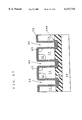
- FIGS. 65 to 72 are cross-sectional views showing a conventional process for forming a trench MOS gate portion in step-by-step fashion.
- FIG. 72 is a cross-sectional view when a trench MOS gate portion 131 has been formed.
- a doped P type region 2 is initially formed on an upper surface of a semiconductor substrate 1 made of Si and the like.
- a heavily doped N type region 3 is selectively formed in an upper surface of the doped P type region 2.
- An oxide film 21 is formed on top of the structure thus obtained. Then a trench 4 is formed which extends through the oxide film 21, the doped P type region 2, and the heavily doped N type region 3 (FIG. 65).
- a silicon oxide film 7 is formed in the trench 4 (FIG. 66). After the oxide films 7 and 21 are removed (FIG. 67), a silicon oxide film is formed as a gate oxide film 9 (FIG. 68).
- the silicon oxide film 7 of 100 to 300 nm in thickness is formed in an atmosphere of oxygen at a temperature ranging from 950 to 1100° C., for example.
- the gate oxide film 9 is generally formed by thermal oxidation in an atmosphere of steam at a temperature not more than 1000° C. This is because the oxide film formed by thermal oxidation in an atmosphere of steam is, in general, less defective than the oxide film formed by thermal oxidation in an atmosphere of oxygen and because the oxide film is less defective at a lower temperature.
- Low-resistance polycrystalline silicon 10 is filled into the trench 4 (FIG. 69) to form a gate electrode 22 in the trench 4.
- a silicon oxide film 11 is formed on the gate electrode 22 (FIG. 70).
- a CVD oxide film 12 is formed on top of the structure provided through the foregoing steps (FIG. 71) and is then shaped by etching into the trench MOS gate portion 131 (FIG. 72).
- the trench 4 after the silicon oxide film 7 is once formed and removed has a characteristic configuration as illustrated in FIG. 67. That is, an opening portion and a bottom of the trench 4 are of angular configurations 5c and 6c, respectively.
- Such configurations of the trench 4 result in a non-uniform thickness of the gate oxide film 9 formed in the trench 4.
- the gate oxide film 9 is most pronouncedly thin in positions reflecting a configuration 5d of the opening portion of the trench 4 and a configuration 6d of the bottom of the trench 4.
- Such reduced thickness of the gate oxide film 9 in the trench 4 particularly in the opening portion and bottom of the trench 4 results in gate breakdown position and breakdown voltage failures.
- a leak current of the gate oxide film 9 increases.
- the angular configurations 5c, 6c of the trench 4 deteriorate the characteristics of the trench MOS gate portion 131.
- defects are prone to occur about the trench 4.
- the defects deteriorate the characteristics of channels formed when a predetermined potential is applied to the gate electrode 22, and reduces a mobility in an MOS gate channel which is a basic characteristic of a power device having the trench MOS gate portion 131 due to defects, strain and contamination adjacent an MOS gate interface, resulting in a rise in on state voltage.
- FIGS. 73 to 81 are cross-sectional views showing a process for fabricating lateral IGBTs trench-isolated in an SOI (silicon on insulator) structure in step-by-step fashion.
- substrates 1e and 1d made of silicon and the like are bonded together, with a silicon oxide film 25 therebetween.
- P layers 41 and N + layers 42 are selectively formed in an upper portion of the semiconductor substrate 1e.
- a silicon oxide film 43 is formed over the semiconductor substrate 1e.
- the silicon oxide film 43 is selectively removed so that parts of the P layers 41 and N + layers 42 are exposed (FIG. 74), and silicon etching is performed using the remaining silicon oxide film 43 as a mask. This permits the semiconductor substrate 1e to be selectively excavated down to form trenches 44 (FIG. 75).
- sacrificial oxide films 45 are once selectively formed on inner walls of the trenches 44 by thermal oxidation (FIG. 76), and the silicon oxide films are etched. This permits the removal of parts of the silicon oxide film 25, all of the sacrificial oxide films 45 and all of the silicon oxide film 43, and also permits the trenches 44 to be further excavated down to the level lower than the bottom of the semiconductor substrate 1e (FIG. 77).
- Thermal oxidation in an atmosphere of steam at a temperature not more than 1000° C. provides isolation oxide films 46 around the remaining semiconductor substrate 1e (including the P layers 41 and N + layers 42) (FIG. 78).
- Polycrystalline silicon 47 is deposited over the structure of FIG. 78 to fill the trenches 44 with the polycrystalline silicon 47 (FIG. 79).
- the polycrystalline silicon 47 over the semiconductor substrate 1e is selectively removed so that the polycrystalline silicon 47 remains only in the trenches 44.
- the polycrystalline silicon 47 is covered with field oxide films 48.
- the field oxide films 48 are also formed on the surface of the semiconductor substrate 1e between the P layers 41 and the N + layers 42 (FIG. 80). Then a predetermined doped layer is formed, and lateral IGBTs are formed which are isolated from each other by isolating portions 13a having a trench structure (FIG. 81).
- the isolating portions 13a in this manner causes the problems of the thickness of the isolation oxide films 46 similar to the first background art problems.
- the semiconductor substrate 1e including the P layers 41 and N + layers 42
- the isolation oxide films 46 in these portions are pronouncedly thinner than those in other portions.
- the isolation oxide films 46 are prone to be broken particularly in the bottoms 44b. This causes the problem of a lowered isolation breakdown voltage by the isolating portions 13a.
- the present invention is intended for a method of fabricating a semiconductor device.
- the method comprises the steps of: (a) anisotropically etching a substrate made of semiconductor to form a trench extending in a direction of the thickness of the substrate; (b) performing a first thermal oxidation to form a first sacrificial oxide film in the trench; (c) removing the first sacrificial oxide film; (d) performing a second thermal oxidation to form a second sacrificial oxide film in the trench after the step (c); (e) removing the second sacrificial oxide film; (f) forming an insulating film comprising a part of a control electrode in the trench after the step (e); and (g) filling the trench to form the control electrode opposed to the substrate through the insulating film comprising the part of the control electrode.
- the opening portion and bottom of the trench are rounded by forming the first and second sacrificial oxide films to reduce the defects adjacent the trench. Since acute-angle portions are eliminated at the interface between the semiconductor substrate and the insulating film, the electric field concentration is alleviated in the edges and a uniform electric field distribution is provided.
- the second thermal oxidation is performed in a water-containing atmosphere
- the first thermal oxidation is performed in an atmosphere of oxygen at a first temperature higher than a second temperature at which the second thermal oxidation is performed.
- the bottom of the trench is mainly rounded by the water-containing oxidation.
- the second oxidation completely removes the region including defects and strains concentrated adjacent the surface of the trench by the first oxidation.
- the first temperature is not less than 1000° C.
- the opening portion of the trench is rounded in configuration.
- the opening portion and bottom of the trench are rounded and the defects are decreased adjacent the trench, the electric field concentration is avoided, and a carrier mobility is improved. Therefore, a high-speed operation of the device is enabled.
- the method comprises the steps of: (a) anisotropically etching a substrate made of semiconductor to form a trench having an aspect ratio of from 2 to 30 and extending in a direction of the thickness of the substrate; (b) performing a thermal oxidation in an atmosphere of oxygen at a temperature not less than 1000° C.
- a sacrificial oxide film having a thickness one-tenth to three-tenths the size of an opening portion of the trench; (c) removing the sacrificial oxide film; (d) forming an insulating film comprising a part of a control electrode in the trench after the step (c); and (e) filling the trench to form the control electrode opposed to the substrate through the insulating film comprising the part of the control electrode.
- the thickness of the sacrificial oxide film By suitably controlling the thickness of the sacrificial oxide film, only one formation of the sacrificial oxide film is sufficient. This simplifies the process steps.
- the method comprises the steps of: (a) anisotropically etching a substrate made of semiconductor to form a trench extending in a direction of the thickness of the substrate; (b) performing a thermal oxidation to form a sacrificial oxide film in the trench; (c) removing the sacrificial oxide film; (d) oxidizing an inside of the trench at an atmosphere of oxygen at a temperature not less than 1000° C. to form an insulating film comprising a part of a control electrode after the step (c); and (e) filling the trench to form the control electrode opposed to the substrate through the insulating film comprising the part of the control electrode.
- the opening portion of the trench is rounded by properly adjusting the atmosphere and temperature when the insulating film comprising the part of the control electrode is formed.
- the method comprises the steps of: (a) anisotropically etching a substrate made of semiconductor to form a trench extending in a direction of the thickness of the substrate; (b) providing on the substrate a mask having an edge backing away a predetermined distance from an opening portion of the trench; (c) performing an isotropic dry etching on the substrate by using the mask; (d) oxidizing an inside of the trench in an atmosphere of steam at a temperature not more than 1000° C. after the step (c); and (e) filling the trench to form a control electrode opposed to the substrate through the insulating film comprising the part of the control electrode.
- the opening portion and bottom of the trench are rounded by the isotropic dry etching.
- the distance is 100 to 400 nm.
- the predetermined distance which is not less than 100 nm does not form the angular opening portion of the trench.
- the predetermined distance which is not more than 400 nm prevents the isotropic etching in the opening portion of the trench from proceeding more than necessary in the direction of the thickness of the substrate and in the lateral direction.
- the oxide-based film is deposited by the isotropic etching, thereby smoothing the inner wall of the trench.
- the method further comprises the steps of: (f) performing a thermal oxidation to form a sacrificial oxide film in the trench; and (g) removing the sacrificial oxide film, the steps (f) and (g) being performed after the step (c) and before the step (d).
- the sacrificial oxide film is formed and then removed, providing further rounded opening portion and bottom of the trench.
- the method comprises the steps of: (a) providing a semiconductor layer on a substrate including an insulating film at least on its surface; (b) anisotropically etching the semiconductor layer to form a trench extending in a direction of the thickness of the semiconductor layer; (c) performing a thermal oxidation to form a sacrificial oxide film in the trench; (d) removing a part of the substrate which lies under the trench and the sacrificial oxide film; (e) oxidizing an inside of the trench in an atmosphere of oxygen at a temperature not less than 1000° C. to form an isolation oxide film after the step (d); and (f) filling the trench with a burying material.
- the formation of the isolation oxide film permits the bottom of the trench to be rounded.
- the method comprises the steps of: (a) providing a semiconductor layer on a substrate including an insulating film at least on its surface; (b) anisotropically etching the semiconductor layer to form a trench extending in a direction of the thickness of the semiconductor layer; (c) removing a predetermined distance of a part of the insulating film on the substrate which lies under the trench to form a recess having a diameter greater than a diameter of the trench; (d) performing an isotropic dry etching on the semiconductor layer; (e) oxidizing an inside of the trench in an atmosphere of steam at a temperature not more than 1000° C. to form an isolation oxide film after the step (d); and (f) filling the trench with a burying material.
- the isotropic dry etching permits the bottom of the trench to be rounded.
- the predetermined distance is 100 to 400 nm.
- the predetermined distance which is not less than 100 nm does not form the angular opening portion of the trench.
- the predetermined distance which is not more than 400 nm prevents the isotropic etching in the opening portion of the trench from proceeding more than necessary in the direction of the thickness of the substrate and in the lateral direction.
- the oxide-based film is deposited by the isotropic etching, thereby smoothing the inner wall of the trench.
- the method further comprises the steps of: (g) performing a thermal oxidation to form a sacrificial oxide film in the trench; and (h) removing the sacrificial oxide film, the steps (g) and (h) being performed after the step (d) and before the step (e).
- the sacrificial oxide film is formed and then removed, providing further rounded bottom of the trench.
- the method comprises the steps of: (a) providing a semiconductor layer on a substrate including an insulating film at least on its surface; (b) anisotropically etching the semiconductor layer to form a trench extending in a direction of the thickness of the semiconductor layer; (c) performing a thermal oxidation to form a sacrificial oxide film in the trench; (d) removing a part of the substrate which lies under the trench and the sacrificial oxide film; (e) forming a polycrystalline semiconductor layer on an inner wall of the trench; (f) oxidizing the polycrystalline semiconductor layer to form an isolation oxide film; and (g) filling the trench with a burying material.
- the polycrystalline semiconductor layer covers the corners of the semiconductor layer in the bottom of the trench with good coverage.
- the polycrystalline semiconductor layer is oxidized to provide the isolation oxide film which permits the bottom of the trench to be rounded.
- the method comprises the steps of: (a) providing a semiconductor layer on a substrate including a semiconductor oxide film; (b) anisotropically etching the semiconductor layer to form a trench having an aspect ratio of from 2 to 30 and extending in a direction of the thickness of the semiconductor layer; (c) performing a thermal oxidation in an atmosphere of oxygen at a temperature not less than 1000° C. to form in the trench a sacrificial oxide film having a thickness one-tenth to three-tenths the size of an opening portion of the trench; (d) removing the sacrificial oxide film; (e) forming an isolation oxide film in the trench after the step (c); and (f) filling the trench with a burying material.
- FIGS. 1 to 4 and FIGS. 5A and 5C are cross-sectional views showing a first preferred embodiment in step-by-step fashion according to the present invention
- FIG. 5B is a plan view showing the first preferred embodiment
- FIGS. 5D and 5E are cross-sectional views showing first prior art
- FIG. 6 is a graph illustrating effects of the first preferred embodiment
- FIGS. 7 to 14 are cross-sectional views showing a second preferred embodiment in step-by-step fashion according to the present invention.
- FIGS. 15 and 16 are cross-sectional views illustrating the second preferred embodiment
- FIG. 17 is a graph illustrating the second preferred embodiment
- FIG. 18 is a schematic cross-sectional view illustrating the second preferred embodiment
- FIG. 19 is a graph illustrating the second preferred embodiment
- FIG. 20 is a cross-sectional view of a comparable example
- FIGS. 21 to 23 are cross-sectional views of devices to which the first to third preferred embodiments are applied.
- FIGS. 24 to 28 are plan views of devices to which the first to third preferred embodiments are applied.
- FIGS. 29 to 33 are cross-sectional views of devices to which the first to third preferred embodiments are applied.
- FIGS. 34 to 43 are cross-sectional views showing a fourth preferred embodiment in step-by-step fashion according to the present invention.
- FIG. 44 illustrates effects of the fourth preferred embodiment
- FIGS. 45 and 46 are cross-sectional views showing a sixth preferred embodiment in step-by-step fashion according to the present invention.
- FIGS. 47 to 55 are cross-sectional views showing a seventh preferred embodiment in step-by-step fashion according to the present invention.
- FIGS. 56 to 61 are cross-sectional views showing an eighth preferred embodiment in step-by-step fashion according to the present invention.
- FIG. 62 is a cross-sectional view illustrating the eighth preferred embodiment
- FIGS. 63 and 64 are cross-sectional views illustrating a ninth preferred embodiment according to the present invention.
- FIGS. 65 to 72 are cross-sectional views showing first prior art in step-by-step fashion.
- FIGS. 73 to 81 are cross-sectional views showing second prior art in step-by-step fashion.
- the first fabrication method is a method of fabricating a gate oxide film in a trench which is different from the background art method.
- FIGS. 1 to 5 are cross-sectional views showing a method of forming a trench MOS gate portion 132 in step-by-step fashion according to a first preferred embodiment of the present invention.
- An oxide film 21 is formed on a substrate 1 made of silicon.
- An opening is selectively formed in the oxide film 21, and anisotropic silicon etching is performed using the oxide film 21 as a mask to form a trench 4 extending in a direction of the thickness of the substrate 1 (FIG. 1).
- an opening portion and a bottom of the trench 4 are of angular configurations 5 and 6, respectively.
- a sacrificial oxide film 7 of about 100 to 300 nm in thickness is formed in an atmosphere of oxygen at a temperature ranging from 950 to 1100° C., for example, (FIG. 2) and is then removed (FIG. 3).
- FIGS. 65 to 67 These process steps are similar to those of the first background art shown in FIGS. 65 to 67.
- thermal oxidation in an atmosphere of oxygen at a temperature not less than 1000° C. (for example, 1215° C.) provides a gate oxide film 9 (FIG. 4).
- An oxide film formed by thermal oxidation in an atmosphere of oxygen is more effective in rounding the opening portion 5e of the trench 4 than an oxide film formed by thermal oxidation in an atmosphere of steam when it is formed on an inner wall of the trench after a sacrificial oxide film is formed and then removed.
- FIG. 5A is a cross-sectional view taken along the line A--A of FIG. 5B.
- FIG. 5B is a plan view illustrating the vicinity of the trench MOS gate portion 132.
- FIG. 5C is a cross-sectional view taken along the line B--B of FIG. 5B.
- the plan view of the vicinity of the trench MOS gate portion 131 is also shown in FIG. 5B, but the sections thereof taken along the lines A--A and B--B are shown in FIGS. 5D and 5E, respectively.
- FIG. 6 is a graph illustrating the relation (leak characteristic) between an applied voltage Vg and a leak current Ig when a simple capacitance structure including no diffused layer is formed adjacent the trench.
- the curve G 131 represents the characteristic of the background art trench MOS gate portion 131 shown in FIGS. 5D and 5E wherein the trench has the angular opening portion and bottom
- the curve G 132 represents the characteristic of the trench MOS gate portion 132 shown in FIGS. 5A and 5C to which the present invention is applied.
- the voltage Vg is applied between the substrate 1 and a gate electrode 22.
- the trench MOS gate portion 131 of FIG. 72 is measured when the doped P type region 2 and the heavily doped N type region 3 are not formed on the substrate 1.
- the gate oxide films of the trench MOS gate portions 131, 132 are designed to be about 750 angstroms in thickness.
- the leak characteristic of the trench MOS gate portion 131 abruptly deteriorates when the applied voltage Vg substantially exceeds 30 V. It will be understood that the isolation breakdown voltage for the trench MOS gate portion 131 is about 55 V.
- the leak characteristic of the trench MOS gate portion 132 does not substantially deteriorate when the applied voltage exceeds 40 V, and the isolation breakdown voltage for the trench MOS gate portion 132 is more than 60 V.
- the improved configuration of the trench 4 permits the trench MOS gate portion 132 to have the improved leak characteristic and improved isolation breakdown voltage over the trench MOS gate portion 131 of the first background art.
- the second fabrication method is a technique for smoothing the trench configuration by isotropic plasma etching.
- FIGS. 7 to 14 are cross-sectional views showing a method of forming a trench MOS gate portion 133 in step-by-step fashion according to a second preferred embodiment of the present invention associated with claims 6 to 9.
- the structure shown in FIG. 7 is formed in the same manner as the first preferred embodiment.
- the opening portion and bottom of the trench 4 are of angular configurations 5 and 6, respectively.
- the oxide film 21 is removed selectively in a portion adjacent the opening of the trench 4 so that the oxide film 21 backs away a distance x from the trench 4 (FIG. 7). Then isotropic plasma etching is performed on silicon using an O 2 /CF 4 based gas. The result is a chamfered opening portion of the trench 4 and a rounded bottom configuration 6e thereof having no angular portions. At this time, an oxide-based film 91 is produced adjacent the bottom of the trench 4 as will be described later in detail (FIG. 8).
- the sacrificial oxide film 7 is once formed (FIG. 9) and is then removed, thereby providing a more smoothed configuration 5f of the opening portion of the trench 4 (FIG. 10).
- the configuration 5f sometimes has a linear portion U.
- the linear portion U and the upper surface of the substrate 1 form an angle ⁇ which falls within the range of 30 to 60 degrees.
- a tangent line drawn from a portion of the configuration 5f which has the smallest radius of curvature and the upper surface of the substrate 1 form an angle ⁇ which falls within the range of 30 to 60 degrees.
- the gate oxide film 9 is formed by thermal oxidation in an atmosphere of steam at a temperature not more than 1000° C. (for example, 950° C.) (FIG. 11).
- the thermal oxidation is performed in the atmosphere of oxygen at the temperature not less than 1000° C. for the purpose of forming the gate oxide film 9.
- thermal oxidation in the atmosphere of steam at the temperature not more than 1000° C. provides better characteristics. The reasons therefor is not evident at the present time.
- the trench 4 is filled with low-resistance polycrystalline silicon and the gate electrode 22 is formed.
- a silicon oxide film 11 is formed on the gate electrode, and an oxide film 12 is deposited over the top surface by the CVD process, for example. Further, the gate oxide film 9 and the oxide film 12 are selectively left by etching to form the trench MOS gate portion 133 (FIG. 12).
- the gate electrode 22 may extend to a higher level than the upper surface of the substrate 1 as shown in FIGS. 13 and 14.
- metal films W, Mo, Al, Ti
- metallic compounds WSi, MoSi 2 , AlSi, TiSi
- the leak characteristic of the trench MOS gate portion 133 formed in this manner is represented as the curve G 133 of FIG. 6.
- the leak characteristic of the trench MOS gate portion 133 is about an order of magnitude less than that of the trench MOS gate portion 132 of the first preferred embodiment when the applied voltage Vg is low (not more than 40 V), but is greater when the applied voltage Vg is high (not less than 50 V). That is, when the present invention is applied to a device having a main breakdown voltage which is less than the isolation breakdown voltage of the gate oxide film, the trench MOS gate portion 132 is more suitable than the trench MOS gate portion 133. Conversely, when the present invention is applied to a device having a main breakdown voltage which is more than the isolation breakdown voltage of the gate oxide film, the trench MOS gate portion 133 is more suitable than the trench MOS gate portion 132.
- the leak characteristic of the resultant trench MOS gate portion is substantially equal to or less than that of the trench MOS gate portion 132 when the applied voltage Vg is high (not less than 50 V).
- FIGS. 15 and 16 are cross-sectional views on an enlarged scale illustrating the opening portion of the trench 4 after the isotropic plasma etching when the distance x is less than 100 nm and when the distance x is greater than 400 nm, respectively.
- the broken lines of FIGS. 15 and 16 indicate the configuration of the substrate 1 before the isotropic plasma etching.
- the opening portion of the trench 4 has an angular edge 51.
- the etching proceeds in the direction of the thickness of the substrate 1, and the opening portion of the trench 4 directly reflects the configuration of the oxide film 21 and is not chamfered. Therefore the distance x preferably ranges from 100 nm to 400 nm.
- FIG. 17 is a graph illustrating how a silicon etching rate and a deposition rate of the oxide-based film vary as the ratio R of the gas varies. The graph shows that, as the ratio R of the gas increases, the etching rate decreases and the deposition rate of the film increases.
- FIG. 18 is a schematic cross-sectional view of an etched surface of silicon (for example, the substrate 1) in exaggeration when R is greater than 1.
- the broken lines of FIG. 18 indicate the configuration of the silicon before etching.
- the deposition of an oxide-based film 92 permits recesses to be filled, and etching eliminates projections. As a result, the configuration of the etched surface is considered to be smoothed.
- the silicon etching rate is generally equal to the deposition rate of the oxide-based film.
- the substantial etching rate is not more than 15 nm/min. and it takes tens of minutes for 200 to 300 nm etching required to chamfer the opening portion of the trench 4. This significantly reduces the productivity and makes it difficult to control the sample temperatures during etching, which is not practical.
- the ratio R is preferably less than 5.
- the film deposition simultaneous with the silicon etching allows the inner wall of the trench 4 to be smoothed, and the breakdown voltage of the trench MOS gate portion 133 is considered to increase.
- FIG. 19 is a graph illustrating how the breakdown voltage of the trench MOS gate portion 133 varies with variation in the ratio R of the gas.
- the breakdown voltage is actually measured when R is not more than 3 but is not measured when R is more than 3.
- the upper branch L1 of the graph indicates a breakdown voltage expected from the deposition rate of the oxide-based film
- the lower branch L2 is a breakdown voltage expected from the etching rate.
- a breakdown voltage in a region between the branches L1 and L2 is expected to be obtained in practice.
- a leak characteristic of a trench MOS gate portion 134 formed in this case is represented by the curve G 134 of FIG. 6.
- the leak characteristic of the trench MOS gate portion 134 is less than that of the trench MOS gate portion 133 while the trench MOS gate portion 134 provides a lower leak current and a higher breakdown voltage than the trench MOS gate portion 131. This is considered to result from the fact that the configuration of the opening portion of the trench is further rounded by the step of forming and removing the sacrificial oxide film 7.
- a large displacement current generated at the gate during the turn-on and turn-off operations requires the increase in gate breakdown voltage, and the application of the second preferred embodiment is preferable.
- the leak current Ig is less than about 10 -8 A, there is a small difference in leak characteristic between the trench MOS gate portions 133 and 134.
- the trench MOS gate portion 134 requiring fewer process steps is more advantageous than the trench MOS gate portion 133 in terms of cost versus actual performance.
- the second and third preferred embodiments may be used and applied depending on the purposes of devices to be applied.
- FIG. 20 is a cross-sectional view illustrating the MOS gate structure 135.
- the gate oxide film 9 surrounded by an isolation oxide film F is formed on the substrate 1, and the gate electrode 22 is formed on the gate oxide film 9.
- the gate electrode 22 is covered with the silicon oxide film 11.
- the gate oxide film 9 is formed by thermal oxidation in an atmosphere of steam at a temperature not more than 1000° C., like the second preferred embodiment.
- the voltage Vg is applied between the substrate 1 and the gate electrode 22.
- trench MOS gate portions 132, 133, 134 provide desirable characteristics which are somewhat inferior to but close to the characteristics of the MOS gate structure 135.
- the trench MOS gate portions 132, 133, 134 of the first to third preferred embodiments may be applied to various vertical power devices.
- FIG. 21 is a cross-sectional view of a trench gate type MOSFET 100.
- a doped P type region 2 is formed on the N type semiconductor substrate 1, and a heavily doped N type region 3 is formed selectively in an upper surface of the doped P type region 2.
- a trench extends through the doped P type region 2 and heavily doped N type region 3 into the N type semiconductor substrate 1 to form a trench MOS gate portion 13.
- Source electrodes 14a are formed on the doped P type region 2 and in contact with the heavily doped N type region 3.
- a drain electrode 14c is formed in contact with the N type semiconductor substrate 1. The present invention may be applied to this trench MOS gate portion 13 to improve the leak characteristic.
- FIG. 22 is a cross-sectional view of another trench gate type MOSFET 200.
- the trench gate type MOSFET 200 comprises an N + layer 1b between the drain electrode 14c and the N type semiconductor substrate 1.
- the present invention may be also applied to such a device.
- the trench gate MOSFETs represent an improvement over the conventional MOSFETs in that a higher degree of integration decreases an on-state resistance.
- the application of the trench MOS gate portion forming method of the present invention to such power devices has the effect of improving the gate breakdown voltage because of suppressed electric field concentration adjacent the gate electrode 22.
- FIG. 23 is a cross-sectional view of a trench gate type IGBT (insulated gate bipolar transistor) 300.
- the trench gate type IGBT 300 comprises a P + layer 1c formed on a lower surface (a surface on which the N type semiconductor substrate 1 is not formed) of the N + layer 1b of the trench gate type MOSFET 200.
- a collector electrode 14b is formed in contact with the P + layer 1c.
- the source electrodes 14a for the trench gate type MOSFET 200 function as an emitter electrode for the trench gate type IGBT 300.
- a channel region 15 is formed in the doped P type region 2 around the gate oxide film 9 by the application of a predetermined potential to the gate electrode 22.
- FIGS. 24 to 27 are plan views showing the top structures of the trench gate type IGBTs and trench gate type MOSFETs.
- the trench gate type MOSFETs 100, 200 and the trench gate type IGBT 300 may be constructed as shown in the plan views of FIGS. 24 to 27.
- the top structures shown in FIGS. 26 and 27 have some differences in cross-section from the structures shown in FIGS. 22 and 23.
- FIG. 28 illustrates a part of FIG. 26.
- FIGS. 29 and 30 are cross-sectional views taken along the lines A--A and B--B of FIG. 28.
- FIGS. 29 and 30 differ in construction from FIG. 22.
- FIG. 31 is a cross-sectional view of a lateral trench gate type MOSFET 400 having the trench MOS gate portion 13.
- the lateral trench gate type MOSFET 400 differs from the trench gate type MOSFET 200 of FIG. 22 in that the N + layer 1b and the drain electrode 14c are not formed and that one of the electrodes 14a serves as a source electrode and the other as a drain electrode.
- FIG. 32 is a cross-sectional view of a trench type MCT (MOS controlled thyristor) 500.
- the fabrication method of the first to third preferred embodiments may be applied to the trench MOS gate portions 13 of these devices. Since the damages to and contamination on the inner wall of the trench 4 which are produced by anisotropic etching are removed, the carrier mobility in the channel is improved. This reduces the channel resistance in the on state to reduce the on-state resistance of the whole device.
- FIG. 33 is a cross-sectional view of a trench type diode 600.
- a positive potential is not applied to the gate electrode 22 in the on state but a negative potential is applied thereto in the off state.
- the use of the trench MOS gate portion 13 formed by the fabrication method of the first to third preferred embodiments avoids the electric field concentration.
- the third fabrication method is a technique for forming the sacrificial oxide film twice.
- FIGS. 34 to 43 are cross-sectional views showing a process for forming a trench MOS gate portion in step-by-step fashion according to a fourth preferred embodiment of the present invention.
- the doped P type region 2 and the heavily doped N type region 3 are formed on the substrate 1, and the oxide film 21 is formed on top of the regions 2 and 3 in the same manner as the background art.
- An opening is cut selectively in the oxide film 21 on the heavily doped N type region 3.
- the trench 4 extending through the doped P type region 2 and the heavily doped N type region 3 is formed by anisotropic etching (FIG. 34). At this point of time, the opening portion and bottom of the trench 4 are of angular configurations 5 and 6, respectively.
- the silicon oxide film 7 is formed in the trench 4 in an atmosphere of oxygen at a relatively high temperature T H .
- the temperature T H is not less than 1000° C., for example 1100° C.
- the atmosphere used herein is, for example, an atmosphere of 100% oxygen. Since a soft oxide film is formed at an temperature of 1000° C. or more, the opening portion of the trench 4 has a rounded configuration as designated at 5g.
- the silicon oxide films 7 and 21 are removed by etching (FIG. 36).
- a silicon oxide film 8 is formed in the trench 4 in an atmosphere of steam (FIG. 37). Formation of the silicon oxide film 8 under such conditions provides a rounded configuration 6b of the bottom of the trench 4 and a further rounded configuration 5b of the opening portion of the trench 4.
- a temperature T L used at this time is lower than the temperature T H and is, for example, 950° C.
- the thickness of the silicon oxide films 7, 8 may be selected to be on the order of one-twentieth to one-fifth the opening size. That is, the thickness of the silicon oxide films 7, 8 to be formed relative to the trench 4 of 1 ⁇ m in width is selected to be on the order of 50 to 200 nm, for example 100 nm.
- the silicon oxide film 8 is removed by etching.
- the two processes of forming and removing the silicon oxide films 7, 8 under the above-mentioned conditions allow the trench 4 to have the opening portion and bottom of rounded configurations as designated at 5b and 6b.
- a silicon oxide film is formed in the trench 4 as the gate oxide film 9 (FIG. 39).
- the rounded configurations of the opening portion and bottom of the trench 4 prevent a phenomenon in which the gate oxide film 9 is partially thin as having occurred in the background art and allow the gate oxide film 9 to be formed uniformly in the trench 4.
- low-resistance polycrystalline silicon 10 is deposited on top of the structure provided through the foregoing steps, and the trench 4 is filled with the low-resistance polycrystalline silicon 10 through the gate oxide film 9 (FIG. 40).
- the low-resistance polycrystalline silicon 10 is selectively left by etching technique to form the gate electrode 22 made of the low-resistance polycrystalline silicon 10 in the trench 4.
- the silicon oxide film 11 is formed on the gate electrode 22 (FIG. 41), and the oxide film 12 is deposited over the top surface by CVD process, for example (FIG. 42).
- the oxide film 12 is selectively left by etching to form the trench MOS gate portion 13 (FIG. 43).
- the defects subjected to the gettering effect into the vicinity of the inner wall of the trench 4 are drawn into the silicon oxide film 8.
- the defects of the semiconductor about the trench 4 are reduced as compared with the background art.
- the defect reduction can improve the mobility of carriers in channels to be formed in the semiconductor about the trench 4 when a predetermined potential is applied to the gate electrode 22.
- the on-state voltage is improved by applying the fabrication method of the fourth preferred embodiment to the formation of the trench MOS gate portion 13 of the trench gate type IGBT 300 of FIG. 23.
- FIG. 44 illustrates an on state voltage which is a basic characteristic of the trench gate type IGBT.
- the on state voltage of the trench gate type IGBT 100 is provided by the application of the present invention, and it is 1.44 V.
- the on state voltage of the trench gate type IGBT having the trench MOS gate portion is provided by interchanging the first and second sacrificial oxidation conditions, and it is 1.63 V.
- the on state voltage of the trench gate type IGBT having the trench MOS gate portion is provided by the conventional fabrication method, and it is 1.64 V. It should be noted that a turn-off time is constant (200 ns) under the respective conditions.
- the method of forming the trench MOS gate portion of the fourth preferred embodiment can reduce the on-state voltage of the trench gate type IGBT. This significantly improves power loss.
- the trench 4 has the rounded configuration, and contamination of the substrate 1 on the trench inner wall, defects adjacent the trench, and residual stress are reduced. This improves the interface state and carrier mobility in the channel regions 15 to enhance the characteristics of the trench MOS gate. The result is a reduction in on state voltage which is a basic characteristics of power devices, an improved switching characteristic and, accordingly, a reduction in power loss.
- the fabrication method of the fourth preferred embodiment may be applied to the trench gate type MOSFETs 100, 200 of FIGS. 21, 22, the lateral trench gate type MOSFET 400 of FIG. 31, and the trench type MCT 500 of FIG. 32.
- the application of the fourth preferred embodiment to such power devices represents an improvement which is an increased electron mobility in the channel region 15.
- the fourth preferred embodiment may be also applied to the trench type diode 600 of FIG. 33.
- the thickness of the silicon oxide film 7 formed by the first sacrificial oxidation is selected to be on the order of one-twentieth to one-fifth the opening size of the trench 4 in the fourth preferred embodiment. Selection of the thickness which is not less than one-tenth the opening size affords a further rounded configuration of the opening portion of the trench 4 to improve the breakdown voltage of the gate oxide film 9 without the second sacrificial oxidation and silicon oxide film 8. Thus, the process steps are simplified.
- the thickness of the silicon oxide film 7 is selected to be not more than three-tenths the opening size of the trench 4 so that the trench 4 is filled up and the bottom of the trench 4 is not warped.
- the semiconductor substrate 1 may be made up of a semiconductor compound such as SiC x (0 ⁇ x ⁇ 1), SiGe y (0 ⁇ y ⁇ 1) or the like, thereby providing further advantages.
- the substrate When SiC x is used as a substrate, the substrate may be used at a high temperature because of its great band gap, and a device for a high breakdown voltage is reduced in thickness.
- the use of SiGe y permits a high-speed operation of the device because of its small band gap and great mobility.
- the fourth fabrication method is a technique for trench isolation in the SOI structure.
- a sixth preferred embodiment provides a technique for forming an oxide film on the trench inner wall in an atmosphere of oxygen at a temperature not less than 1000° C., like the first preferred embodiment.
- substrates 1e and 1d made of silicon and the like are bonded together, with a silicon oxide film 25 therebetween.
- P layers 41 and N + layers 42 are selectively formed in an upper portion of the semiconductor substrate 1e.
- a silicon oxide film 43 is formed over the semiconductor substrate 1e (FIG. 73).
- the silicon oxide film 43 is selectively removed so that parts of the P layers 41 and N + layers 42 are exposed (FIG. 74), and silicon etching is performed using the remaining silicon oxide film 43 as a mask. This permits the semiconductor substrate 1e to be selectively excavated down to form trenches 44 (FIG. 75).
- sacrificial oxide films 45 are once formed on inner walls of the trenches 44 by thermal oxidation (FIG. 76), and the silicon oxide films are etched. This permits the removal of parts of the silicon oxide film 25, all of the sacrificial oxide films 45 and all of the silicon oxide film 43, and also permits the trenches 44 to be further excavated down to the level lower than the bottom of the semiconductor substrate 1e (FIG. 77).
- FIG. 45 is a cross-sectional view of the structure provided in the above described process steps in the sixth preferred embodiment.
- the corners of the semiconductor substrate 1e are rounded by the formation of the isolation oxide films 46 like the first preferred embodiment.
- bottoms 44c of the trenches 44 are more rounded than the bottoms 44b of FIG. 78.
- FIG. 46 is a cross-sectional view of the lateral IGBTs fabricated in this manner.
- isolating portions 13b having a trench structure include the isolation oxide films 46 which are not locally thin as compared with the isolating portions 13a of the second background art. This solves the problem of the decrease in isolation breakdown voltage.
- FIGS. 47 to 55 are cross-sectional views illustrating a method of fabricating a semiconductor device in step-by-step fashion according to a seventh preferred embodiment of the present invention.
- FIG. 75 The structure of FIG. 75 is initially obtained in the same manner as the second background art. Isotropic etching is performed on the silicon oxide films to laterally etch and back away the silicon oxide films 43 serving as a trench etching mask and to form recesses 61 in the silicon oxide film 25 under the trenches 44. The comers of the substrate 1e are exposed a distance x in the recesses 61 (FIG. 47).
- isotropic silicon etching is performed to round the comers of the substrate 1e exposed in the recesses 61 and chamfer bottoms 44e of the trenches 44.
- the oxide-based films deposited by the isotropic silicon etching are removed (FIG. 48).
- the distance x is preferably 100 to 400 nm.
- the etching gas is an O 2 /CF 4 based gas, and the ratio R preferably satisfies 1 ⁇ R ⁇ 5.
- the sacrificial oxide films 45 are once formed on the inner walls of the trenches 44 by thermal oxidation (FIG. 49), and the silicon oxide films are etched. This permits the removal of all of the sacrificial oxide films 45 and silicon oxide film 43 and also permits bottoms 44f of the trenches 44 to be further rounded (FIG. 50).
- Thermal oxidation in an atmosphere of steam at a temperature not more than 1000° C. provides the isolation oxide films 46 around the remaining semiconductor substrate 1e (including the P layers 41 and N + layers 42) (FIG. 51).
- the polycrystalline silicon 47 is deposited over the structure of FIG. 51 to fill the trenches 44 (including the recesses 61) with the polycrystalline silicon 47 (FIG. 52).
- the polycrystalline silicon 47 over the semiconductor substrate 1e is selectively removed so that the polycrystalline silicon 47 remains only in the trenches 44 (FIG. 53).
- the polycrystalline silicon 47 is covered with the field oxide films 48.
- the field oxide films 48 are also formed on the surface of the semiconductor substrate 1e between the P layers 41 and the N + layers 42 (FIG. 54). Then a predetermined doped layer is formed, and the lateral IGBTs are formed which are isolated from each other by isolating portions 13c having a trench structure (FIG. 55).
- the isolation oxide films 46 are not locally thin. This solves the problem of the decrease in isolation breakdown voltage.
- the silicon oxide film 43 may back away a distance y from the opening portion of the trenches 44. If the silicon oxide film 43 is sufficiently thick relative to the distance x, the silicon oxide film 43 need not be covered with a resist. As a result, since the distance y is generally equal to the distance x if the P layers 41 and the N + layers 42 are exposed the distance y around the trenches 44, opening portions 44d of the trenches 44 are also rounded by the isotropic silicon etching. This is a secondary preferable effect of the present invention. However, the opening portions 44d are subsequently covered with the filed oxide films 48, and the effect of the present invention is not prevented.
- the isolation oxide films 46 are prevented from becoming locally thin as compared with the second background art since the bottoms 44e of the trenches 44 are chamfered if the process steps of forming and removing the sacrificial oxide films 45 like the third preferred embodiment.
- FIGS. 56 to 61 are cross-sectional views illustrating a method of fabricating a semiconductor device in step-by-step fashion according to an eighth preferred embodiment of the present invention.
- FIG. 77 The structure of FIG. 77 is initially obtained in the same manner as the second background art.
- the silicon oxide film 25 is etched to a depth of about 200 to 300 nm, for example, to form the extending trenches 44.
- Polycrystalline silicon 71 is deposited to a thickness of 200 to 300 nm over the top surface. Then, the polycrystalline silicon 71 is exposed on the inner surfaces of the trenches 44 (FIG. 56).
- polycrystalline silicon has a good step coverage and covers the corners of the trenches 44 if the corners of the substrate 1e are projecting in the bottoms 44b of the trenches 44.
- the silicon oxide film 72 serving as an isolation oxide film has a thickness of 200 to 300 nm and is not locally thin.
- the polycrystalline silicon 47 is deposited in the same manner as the second background art and the seventh preferred embodiment to fill the trenches 44 with the polycrystalline silicon 47 (FIG. 58).
- the polycrystalline silicon 47 over the semiconductor substrate 1e is selectively removed so that the polycrystalline silicon 47 remains only in the trenches 44 (FIG. 59).
- the polycrystalline silicon 47 is covered with the field oxide films 48 (FIG. 60).
- a predetermined doped layer is formed, and the lateral IGBTs are formed which are isolated from each other by isolating portions 13d having a trench structure (FIG. 61).
- the isolating portions 13b, 13c, 13d are used for isolation of the lateral IGBTs from each other in the sixth to eighth preferred embodiments.
- the sixth to eighth preferred embodiments may be applied to the isolation of different devices from each other.
- FIG. 62 is a cross-sectional view of a lateral diode, a lateral IGBT, and an MOSFET isolated from each other, and illustrates the application of the sixth and seventh preferred embodiments.
- the substrate 1e is rounded in the bottoms of the isolating portions. In these portions, the silicon oxide film is not locally thin.
- FIG. 63 is a cross-sectional view of a lateral IGBT 700 in a high-voltage power IC which is provided by applying the trench formation process of the fourth preferred embodiment to trench isolation.
- the lateral IGBT 700 is formed in the semiconductor substrate 1e.
- the semiconductor substrate 1e is formed immediately over the silicon oxide film 25 formed on the semiconductor substrate 1d.
- Isolating portions 13e are formed by filling the polycrystalline silicon 10 after silicon oxide films 9a are formed. It should be noted that the polycrystalline silicon 10 does not function as a gate but the isolating portions 13e are used for isolation between devices.
- All of the isolating portions 13e may be filled with the silicon oxide films 9a and the polycrystalline silicon 10 need not be used when the isolating portions 13e have a small width (for example, 1 ⁇ m or less) or when the isolating portions 13e are wide but a thick CVD silicon oxide film is formed for a short time (for example, several hours). Further, another film (for example, silicon nitride film) may be substituted for the polycrystalline silicon 10.
- Formation of the isolating portions 13e by using the trench formation process of the fourth preferred embodiment is advantageous in that leakage is reduced in the isolating portions.
- FIG. 64 is a cross-sectional view of a lateral diode, a lateral IGBT, and an MOSFET isolated from each other in the same manner as in FIG. 62, and illustrates the application of the ninth preferred embodiment.
Abstract
A method of fabricating a semiconductor device which includes the steps of forming a trench (4), and repeating the formation and removal of an oxide film (a sacrificial oxide film) twice to provide a rounded configuration (5b) of an opening portion of the trench (4) and a rounded configuration (6b) of a bottom thereof and to draw defects in a semiconductor layer into a silicon oxide film (8), reducing the defects adjacent the inner wall of the trench (4), whereby electric field concentration on a gate is prevented and the mobility of carriers in channels is improved for an improvement in characteristic, particularly an on-state voltage, of a power device.
Description
This application is a continuation of Ser. No. 08/382,581 filed Feb. 2, 1995 now U.S. Pat. No. 5,783,491.
1. Field of the Invention
The present invention relates to a technique for forming a trench MOS gate to be applied to a semiconductor device, particularly to a power device. The invention also relates to a device isolation technique.
2. Description of the Background Art
A. Background Art
(a-1) First Background Art and Problems thereof
FIGS. 65 to 72 are cross-sectional views showing a conventional process for forming a trench MOS gate portion in step-by-step fashion. In particular, FIG. 72 is a cross-sectional view when a trench MOS gate portion 131 has been formed.
Referring to FIG. 65, a doped P type region 2 is initially formed on an upper surface of a semiconductor substrate 1 made of Si and the like. A heavily doped N type region 3 is selectively formed in an upper surface of the doped P type region 2. An oxide film 21 is formed on top of the structure thus obtained. Then a trench 4 is formed which extends through the oxide film 21, the doped P type region 2, and the heavily doped N type region 3 (FIG. 65).
A silicon oxide film 7 is formed in the trench 4 (FIG. 66). After the oxide films 7 and 21 are removed (FIG. 67), a silicon oxide film is formed as a gate oxide film 9 (FIG. 68).
An oxide film which is removed immediately after it is formed, such as the silicon oxide film 7, is referred to as a "sacrificial oxide film" hereinafter. For shaping of the trench and removal of defects, strain and contamination in the trench, the sacrificial oxide film is sacrificed without remaining in a structure to be completed later. The silicon oxide film 7 of 100 to 300 nm in thickness is formed in an atmosphere of oxygen at a temperature ranging from 950 to 1100° C., for example.
The gate oxide film 9 is generally formed by thermal oxidation in an atmosphere of steam at a temperature not more than 1000° C. This is because the oxide film formed by thermal oxidation in an atmosphere of steam is, in general, less defective than the oxide film formed by thermal oxidation in an atmosphere of oxygen and because the oxide film is less defective at a lower temperature.
Low-resistance polycrystalline silicon 10, for example, is filled into the trench 4 (FIG. 69) to form a gate electrode 22 in the trench 4. A silicon oxide film 11 is formed on the gate electrode 22 (FIG. 70). A CVD oxide film 12 is formed on top of the structure provided through the foregoing steps (FIG. 71) and is then shaped by etching into the trench MOS gate portion 131 (FIG. 72).
The trench 4 after the silicon oxide film 7 is once formed and removed has a characteristic configuration as illustrated in FIG. 67. That is, an opening portion and a bottom of the trench 4 are of angular configurations 5c and 6c, respectively.
Such configurations of the trench 4 result in a non-uniform thickness of the gate oxide film 9 formed in the trench 4. In particular, the gate oxide film 9 is most pronouncedly thin in positions reflecting a configuration 5d of the opening portion of the trench 4 and a configuration 6d of the bottom of the trench 4.
Such reduced thickness of the gate oxide film 9 in the trench 4 particularly in the opening portion and bottom of the trench 4 results in gate breakdown position and breakdown voltage failures. In addition, a leak current of the gate oxide film 9 increases.
Further, the angular configurations 5c, 6c of the trench 4 deteriorate the characteristics of the trench MOS gate portion 131. In the step of forming the trench 4, defects are prone to occur about the trench 4. The defects deteriorate the characteristics of channels formed when a predetermined potential is applied to the gate electrode 22, and reduces a mobility in an MOS gate channel which is a basic characteristic of a power device having the trench MOS gate portion 131 due to defects, strain and contamination adjacent an MOS gate interface, resulting in a rise in on state voltage.
(a-2) Second Background Art and Problems thereof
FIGS. 73 to 81 are cross-sectional views showing a process for fabricating lateral IGBTs trench-isolated in an SOI (silicon on insulator) structure in step-by-step fashion.
Referring to FIG. 73, substrates 1e and 1d made of silicon and the like are bonded together, with a silicon oxide film 25 therebetween. P layers 41 and N+ layers 42 are selectively formed in an upper portion of the semiconductor substrate 1e. A silicon oxide film 43 is formed over the semiconductor substrate 1e.
The silicon oxide film 43 is selectively removed so that parts of the P layers 41 and N+ layers 42 are exposed (FIG. 74), and silicon etching is performed using the remaining silicon oxide film 43 as a mask. This permits the semiconductor substrate 1e to be selectively excavated down to form trenches 44 (FIG. 75).
Then, sacrificial oxide films 45 are once selectively formed on inner walls of the trenches 44 by thermal oxidation (FIG. 76), and the silicon oxide films are etched. This permits the removal of parts of the silicon oxide film 25, all of the sacrificial oxide films 45 and all of the silicon oxide film 43, and also permits the trenches 44 to be further excavated down to the level lower than the bottom of the semiconductor substrate 1e (FIG. 77). Thermal oxidation in an atmosphere of steam at a temperature not more than 1000° C. provides isolation oxide films 46 around the remaining semiconductor substrate 1e (including the P layers 41 and N+ layers 42) (FIG. 78).
Construction of the isolating portions 13a in this manner causes the problems of the thickness of the isolation oxide films 46 similar to the first background art problems. Specifically, as shown in FIG. 78, the semiconductor substrate 1e (including the P layers 41 and N+ layers 42) is of an angular configuration in opening portions 44a and bottoms 44b of the trenches 44. The isolation oxide films 46 in these portions are pronouncedly thinner than those in other portions. The isolation oxide films 46 are prone to be broken particularly in the bottoms 44b. This causes the problem of a lowered isolation breakdown voltage by the isolating portions 13a.
The present invention is intended for a method of fabricating a semiconductor device. According to the present invention, the method comprises the steps of: (a) anisotropically etching a substrate made of semiconductor to form a trench extending in a direction of the thickness of the substrate; (b) performing a first thermal oxidation to form a first sacrificial oxide film in the trench; (c) removing the first sacrificial oxide film; (d) performing a second thermal oxidation to form a second sacrificial oxide film in the trench after the step (c); (e) removing the second sacrificial oxide film; (f) forming an insulating film comprising a part of a control electrode in the trench after the step (e); and (g) filling the trench to form the control electrode opposed to the substrate through the insulating film comprising the part of the control electrode.
The opening portion and bottom of the trench are rounded by forming the first and second sacrificial oxide films to reduce the defects adjacent the trench. Since acute-angle portions are eliminated at the interface between the semiconductor substrate and the insulating film, the electric field concentration is alleviated in the edges and a uniform electric field distribution is provided.
Preferably, the second thermal oxidation is performed in a water-containing atmosphere, and the first thermal oxidation is performed in an atmosphere of oxygen at a first temperature higher than a second temperature at which the second thermal oxidation is performed.
The bottom of the trench is mainly rounded by the water-containing oxidation. The second oxidation completely removes the region including defects and strains concentrated adjacent the surface of the trench by the first oxidation.
Preferably, the first temperature is not less than 1000° C.
Thus the opening portion of the trench is rounded in configuration.
As above described, since the opening portion and bottom of the trench are rounded and the defects are decreased adjacent the trench, the electric field concentration is avoided, and a carrier mobility is improved. Therefore, a high-speed operation of the device is enabled.
In another aspect of the present invention, the method comprises the steps of: (a) anisotropically etching a substrate made of semiconductor to form a trench having an aspect ratio of from 2 to 30 and extending in a direction of the thickness of the substrate; (b) performing a thermal oxidation in an atmosphere of oxygen at a temperature not less than 1000° C. to form in the trench a sacrificial oxide film having a thickness one-tenth to three-tenths the size of an opening portion of the trench; (c) removing the sacrificial oxide film; (d) forming an insulating film comprising a part of a control electrode in the trench after the step (c); and (e) filling the trench to form the control electrode opposed to the substrate through the insulating film comprising the part of the control electrode.
By suitably controlling the thickness of the sacrificial oxide film, only one formation of the sacrificial oxide film is sufficient. This simplifies the process steps.
In a third aspect of the present invention, the method comprises the steps of: (a) anisotropically etching a substrate made of semiconductor to form a trench extending in a direction of the thickness of the substrate; (b) performing a thermal oxidation to form a sacrificial oxide film in the trench; (c) removing the sacrificial oxide film; (d) oxidizing an inside of the trench at an atmosphere of oxygen at a temperature not less than 1000° C. to form an insulating film comprising a part of a control electrode after the step (c); and (e) filling the trench to form the control electrode opposed to the substrate through the insulating film comprising the part of the control electrode.
The opening portion of the trench is rounded by properly adjusting the atmosphere and temperature when the insulating film comprising the part of the control electrode is formed.
This improves a leak characteristic in the control electrode and reduces a channel resistance.
In a fourth aspect of the present invention, the method comprises the steps of: (a) anisotropically etching a substrate made of semiconductor to form a trench extending in a direction of the thickness of the substrate; (b) providing on the substrate a mask having an edge backing away a predetermined distance from an opening portion of the trench; (c) performing an isotropic dry etching on the substrate by using the mask; (d) oxidizing an inside of the trench in an atmosphere of steam at a temperature not more than 1000° C. after the step (c); and (e) filling the trench to form a control electrode opposed to the substrate through the insulating film comprising the part of the control electrode.
The opening portion and bottom of the trench are rounded by the isotropic dry etching.
This improves the leak characteristic in the control electrode and reduces the channel resistance.
Preferably, the distance is 100 to 400 nm.
The predetermined distance which is not less than 100 nm does not form the angular opening portion of the trench. The predetermined distance which is not more than 400 nm prevents the isotropic etching in the opening portion of the trench from proceeding more than necessary in the direction of the thickness of the substrate and in the lateral direction.
This provides the rounded opening portion of the trench.
Preferably, the isotropic dry etching is performed by using an O2 /CF4 based gas, and a ratio R=O2 /CF4 of the gas satisfies 1<R<5.
The oxide-based film is deposited by the isotropic etching, thereby smoothing the inner wall of the trench.
Preferably, the method further comprises the steps of: (f) performing a thermal oxidation to form a sacrificial oxide film in the trench; and (g) removing the sacrificial oxide film, the steps (f) and (g) being performed after the step (c) and before the step (d).
The sacrificial oxide film is formed and then removed, providing further rounded opening portion and bottom of the trench.
This improves the leak characteristic in the control electrode and reduces the channel resistance.
In a fifth aspect of the present invention, the method comprises the steps of: (a) providing a semiconductor layer on a substrate including an insulating film at least on its surface; (b) anisotropically etching the semiconductor layer to form a trench extending in a direction of the thickness of the semiconductor layer; (c) performing a thermal oxidation to form a sacrificial oxide film in the trench; (d) removing a part of the substrate which lies under the trench and the sacrificial oxide film; (e) oxidizing an inside of the trench in an atmosphere of oxygen at a temperature not less than 1000° C. to form an isolation oxide film after the step (d); and (f) filling the trench with a burying material.
The formation of the isolation oxide film permits the bottom of the trench to be rounded.
This improves the leak characteristic in the isolation oxide film.
In a sixth aspect of the present invention, the method comprises the steps of: (a) providing a semiconductor layer on a substrate including an insulating film at least on its surface; (b) anisotropically etching the semiconductor layer to form a trench extending in a direction of the thickness of the semiconductor layer; (c) removing a predetermined distance of a part of the insulating film on the substrate which lies under the trench to form a recess having a diameter greater than a diameter of the trench; (d) performing an isotropic dry etching on the semiconductor layer; (e) oxidizing an inside of the trench in an atmosphere of steam at a temperature not more than 1000° C. to form an isolation oxide film after the step (d); and (f) filling the trench with a burying material.
The isotropic dry etching permits the bottom of the trench to be rounded.
This improves the leak characteristic in the isolation oxide film.
Preferably, the predetermined distance is 100 to 400 nm.
The predetermined distance which is not less than 100 nm does not form the angular opening portion of the trench. The predetermined distance which is not more than 400 nm prevents the isotropic etching in the opening portion of the trench from proceeding more than necessary in the direction of the thickness of the substrate and in the lateral direction.
This provides the rounded bottom of the trench.
Preferably, the isotropic dry etching is performed by using an O2 /CF4 based gas, and a ratio R=O2 /CF4 of the gas satisfies 1<R<5.
The oxide-based film is deposited by the isotropic etching, thereby smoothing the inner wall of the trench.
Preferably, the method further comprises the steps of: (g) performing a thermal oxidation to form a sacrificial oxide film in the trench; and (h) removing the sacrificial oxide film, the steps (g) and (h) being performed after the step (d) and before the step (e).
The sacrificial oxide film is formed and then removed, providing further rounded bottom of the trench.
This improves the leak characteristic in the isolation oxide film.
In a seventh aspect of the present invention, the method comprises the steps of: (a) providing a semiconductor layer on a substrate including an insulating film at least on its surface; (b) anisotropically etching the semiconductor layer to form a trench extending in a direction of the thickness of the semiconductor layer; (c) performing a thermal oxidation to form a sacrificial oxide film in the trench; (d) removing a part of the substrate which lies under the trench and the sacrificial oxide film; (e) forming a polycrystalline semiconductor layer on an inner wall of the trench; (f) oxidizing the polycrystalline semiconductor layer to form an isolation oxide film; and (g) filling the trench with a burying material.
The polycrystalline semiconductor layer covers the corners of the semiconductor layer in the bottom of the trench with good coverage. The polycrystalline semiconductor layer is oxidized to provide the isolation oxide film which permits the bottom of the trench to be rounded.
This improves the leak characteristic in the isolation oxide film.
In an eighth aspect of the present invention, the method comprises the steps of: (a) providing a semiconductor layer on a substrate including a semiconductor oxide film; (b) anisotropically etching the semiconductor layer to form a trench having an aspect ratio of from 2 to 30 and extending in a direction of the thickness of the semiconductor layer; (c) performing a thermal oxidation in an atmosphere of oxygen at a temperature not less than 1000° C. to form in the trench a sacrificial oxide film having a thickness one-tenth to three-tenths the size of an opening portion of the trench; (d) removing the sacrificial oxide film; (e) forming an isolation oxide film in the trench after the step (c); and (f) filling the trench with a burying material.
By properly controlling the thickness of the sacrificial oxide film, only one formation of the sacrificial oxide film is sufficient. This simplifies the process steps.
It is therefore an object of the present invention to provide a technique for improving characteristics, particularly an on state voltage, of a power device having a trench MOS gate portion through an easy process by enhancing the characteristics of the trench MOS gate portion.
It is another object of the present invention to increase an isolation breakdown voltage in a trench isolation for isolating devices from each other in an SOI (silicon on insulator) structure.
These and other objects, features, aspects and advantages of the present invention will become more apparent from the following detailed description of the present invention when taken in conjunction with the accompanying drawings.
FIGS. 1 to 4 and FIGS. 5A and 5C are cross-sectional views showing a first preferred embodiment in step-by-step fashion according to the present invention;
FIG. 5B is a plan view showing the first preferred embodiment;
FIGS. 5D and 5E are cross-sectional views showing first prior art;
FIG. 6 is a graph illustrating effects of the first preferred embodiment;
FIGS. 7 to 14 are cross-sectional views showing a second preferred embodiment in step-by-step fashion according to the present invention;
FIGS. 15 and 16 are cross-sectional views illustrating the second preferred embodiment;
FIG. 17 is a graph illustrating the second preferred embodiment;
FIG. 18 is a schematic cross-sectional view illustrating the second preferred embodiment;
FIG. 19 is a graph illustrating the second preferred embodiment;
FIG. 20 is a cross-sectional view of a comparable example;
FIGS. 21 to 23 are cross-sectional views of devices to which the first to third preferred embodiments are applied;
FIGS. 24 to 28 are plan views of devices to which the first to third preferred embodiments are applied;
FIGS. 29 to 33 are cross-sectional views of devices to which the first to third preferred embodiments are applied;
FIGS. 34 to 43 are cross-sectional views showing a fourth preferred embodiment in step-by-step fashion according to the present invention;
FIG. 44 illustrates effects of the fourth preferred embodiment;
FIGS. 45 and 46 are cross-sectional views showing a sixth preferred embodiment in step-by-step fashion according to the present invention;
FIGS. 47 to 55 are cross-sectional views showing a seventh preferred embodiment in step-by-step fashion according to the present invention;
FIGS. 56 to 61 are cross-sectional views showing an eighth preferred embodiment in step-by-step fashion according to the present invention;
FIG. 62 is a cross-sectional view illustrating the eighth preferred embodiment;
FIGS. 63 and 64 are cross-sectional views illustrating a ninth preferred embodiment according to the present invention;
FIGS. 65 to 72 are cross-sectional views showing first prior art in step-by-step fashion; and
FIGS. 73 to 81 are cross-sectional views showing second prior art in step-by-step fashion.
B. First Fabrication Method
The first fabrication method is a method of fabricating a gate oxide film in a trench which is different from the background art method.
(b-1) First Preferred Embodiment
FIGS. 1 to 5 are cross-sectional views showing a method of forming a trench MOS gate portion 132 in step-by-step fashion according to a first preferred embodiment of the present invention. An oxide film 21 is formed on a substrate 1 made of silicon. An opening is selectively formed in the oxide film 21, and anisotropic silicon etching is performed using the oxide film 21 as a mask to form a trench 4 extending in a direction of the thickness of the substrate 1 (FIG. 1). At this time, an opening portion and a bottom of the trench 4 are of angular configurations 5 and 6, respectively. Then, a sacrificial oxide film 7 of about 100 to 300 nm in thickness is formed in an atmosphere of oxygen at a temperature ranging from 950 to 1100° C., for example, (FIG. 2) and is then removed (FIG. 3). These process steps are similar to those of the first background art shown in FIGS. 65 to 67.
In the first preferred embodiment, thermal oxidation in an atmosphere of oxygen at a temperature not less than 1000° C. (for example, 1215° C.) provides a gate oxide film 9 (FIG. 4). An oxide film formed by thermal oxidation in an atmosphere of oxygen is more effective in rounding the opening portion 5e of the trench 4 than an oxide film formed by thermal oxidation in an atmosphere of steam when it is formed on an inner wall of the trench after a sacrificial oxide film is formed and then removed.
Subsequent process steps of the first preferred embodiment are similar to those of the first background art. Specifically, the trench MOS gate portion 132 is formed (FIG. 5A). FIG. 5A is a cross-sectional view taken along the line A--A of FIG. 5B. FIG. 5B is a plan view illustrating the vicinity of the trench MOS gate portion 132. FIG. 5C is a cross-sectional view taken along the line B--B of FIG. 5B. In the background art, for example, the plan view of the vicinity of the trench MOS gate portion 131 is also shown in FIG. 5B, but the sections thereof taken along the lines A--A and B--B are shown in FIGS. 5D and 5E, respectively.
FIG. 6 is a graph illustrating the relation (leak characteristic) between an applied voltage Vg and a leak current Ig when a simple capacitance structure including no diffused layer is formed adjacent the trench. The curve G131 represents the characteristic of the background art trench MOS gate portion 131 shown in FIGS. 5D and 5E wherein the trench has the angular opening portion and bottom, and the curve G132 represents the characteristic of the trench MOS gate portion 132 shown in FIGS. 5A and 5C to which the present invention is applied.
The voltage Vg is applied between the substrate 1 and a gate electrode 22. The trench MOS gate portion 131 of FIG. 72 is measured when the doped P type region 2 and the heavily doped N type region 3 are not formed on the substrate 1. The gate oxide films of the trench MOS gate portions 131, 132 are designed to be about 750 angstroms in thickness.
The leak characteristic of the trench MOS gate portion 131 abruptly deteriorates when the applied voltage Vg substantially exceeds 30 V. It will be understood that the isolation breakdown voltage for the trench MOS gate portion 131 is about 55 V.
On the other hand, the leak characteristic of the trench MOS gate portion 132 does not substantially deteriorate when the applied voltage exceeds 40 V, and the isolation breakdown voltage for the trench MOS gate portion 132 is more than 60 V.
The reasons are not evident why the configuration of the trench 4 is improved by changing the conditions under which the gate oxide film 9 is formed from the conventional conditions. However, the improved configuration of the trench 4 permits the trench MOS gate portion 132 to have the improved leak characteristic and improved isolation breakdown voltage over the trench MOS gate portion 131 of the first background art.
C. Second Fabrication Method
The second fabrication method is a technique for smoothing the trench configuration by isotropic plasma etching.
(c-1) Second Preferred Embodiment
FIGS. 7 to 14 are cross-sectional views showing a method of forming a trench MOS gate portion 133 in step-by-step fashion according to a second preferred embodiment of the present invention associated with claims 6 to 9. The structure shown in FIG. 7 is formed in the same manner as the first preferred embodiment. As above described, the opening portion and bottom of the trench 4 are of angular configurations 5 and 6, respectively.
The oxide film 21 is removed selectively in a portion adjacent the opening of the trench 4 so that the oxide film 21 backs away a distance x from the trench 4 (FIG. 7). Then isotropic plasma etching is performed on silicon using an O2 /CF4 based gas. The result is a chamfered opening portion of the trench 4 and a rounded bottom configuration 6e thereof having no angular portions. At this time, an oxide-based film 91 is produced adjacent the bottom of the trench 4 as will be described later in detail (FIG. 8).
After the film 91 and the oxide film 21 are removed, the sacrificial oxide film 7 is once formed (FIG. 9) and is then removed, thereby providing a more smoothed configuration 5f of the opening portion of the trench 4 (FIG. 10). When the opening portion of the trench 4 is shown on an enlarged scale, the configuration 5f sometimes has a linear portion U. In this case, the linear portion U and the upper surface of the substrate 1 form an angle θ which falls within the range of 30 to 60 degrees. When the configuration 5f does not have the linear portion U, a tangent line drawn from a portion of the configuration 5f which has the smallest radius of curvature and the upper surface of the substrate 1 form an angle θ which falls within the range of 30 to 60 degrees.
Then the gate oxide film 9 is formed by thermal oxidation in an atmosphere of steam at a temperature not more than 1000° C. (for example, 950° C.) (FIG. 11). In the first preferred embodiment, the thermal oxidation is performed in the atmosphere of oxygen at the temperature not less than 1000° C. for the purpose of forming the gate oxide film 9. However, after the isotropic plasma etching, thermal oxidation in the atmosphere of steam at the temperature not more than 1000° C. provides better characteristics. The reasons therefor is not evident at the present time.
Then, the trench 4 is filled with low-resistance polycrystalline silicon and the gate electrode 22 is formed. A silicon oxide film 11 is formed on the gate electrode, and an oxide film 12 is deposited over the top surface by the CVD process, for example. Further, the gate oxide film 9 and the oxide film 12 are selectively left by etching to form the trench MOS gate portion 133 (FIG. 12). The gate electrode 22 may extend to a higher level than the upper surface of the substrate 1 as shown in FIGS. 13 and 14.
For the formation of the gate electrode 22, metal films (W, Mo, Al, Ti) and metallic compounds (WSi, MoSi2, AlSi, TiSi) may be substituted for the low-resistance polycrystalline silicon.
The leak characteristic of the trench MOS gate portion 133 formed in this manner is represented as the curve G133 of FIG. 6. The leak characteristic of the trench MOS gate portion 133 is about an order of magnitude less than that of the trench MOS gate portion 132 of the first preferred embodiment when the applied voltage Vg is low (not more than 40 V), but is greater when the applied voltage Vg is high (not less than 50 V). That is, when the present invention is applied to a device having a main breakdown voltage which is less than the isolation breakdown voltage of the gate oxide film, the trench MOS gate portion 132 is more suitable than the trench MOS gate portion 133. Conversely, when the present invention is applied to a device having a main breakdown voltage which is more than the isolation breakdown voltage of the gate oxide film, the trench MOS gate portion 133 is more suitable than the trench MOS gate portion 132.
In the second preferred embodiment, if thermal oxidation is performed in an atmosphere of oxygen at a temperature not less than 1000° C. for the formation of the gate oxide film 9, the leak characteristic of the resultant trench MOS gate portion is substantially equal to or less than that of the trench MOS gate portion 132 when the applied voltage Vg is high (not less than 50 V).
The distance x backed away by the oxide film 21 from the opening portion of the trench 4 is preferably not less than 100 nm and not more than 400 nm. FIGS. 15 and 16 are cross-sectional views on an enlarged scale illustrating the opening portion of the trench 4 after the isotropic plasma etching when the distance x is less than 100 nm and when the distance x is greater than 400 nm, respectively. The broken lines of FIGS. 15 and 16 indicate the configuration of the substrate 1 before the isotropic plasma etching.
With the distance x less than 100 nm, the opening portion of the trench 4 has an angular edge 51. With the distance x greater than 400 nm, the etching proceeds in the direction of the thickness of the substrate 1, and the opening portion of the trench 4 directly reflects the configuration of the oxide film 21 and is not chamfered. Therefore the distance x preferably ranges from 100 nm to 400 nm.
The ratio R=O2 /CF4 of the gas used for the isotropic plasma etching preferably satisfies 1<R<5. FIG. 17 is a graph illustrating how a silicon etching rate and a deposition rate of the oxide-based film vary as the ratio R of the gas varies. The graph shows that, as the ratio R of the gas increases, the etching rate decreases and the deposition rate of the film increases.
When the ratio R is not more than 1, the etching rate is 50 nm/min. and substantially no film is deposited. This does not cause the etching surface to be smoothed but results in a rough surface. When R>1, the etching surface is smoothed. FIG. 18 is a schematic cross-sectional view of an etched surface of silicon (for example, the substrate 1) in exaggeration when R is greater than 1. The broken lines of FIG. 18 indicate the configuration of the silicon before etching. The deposition of an oxide-based film 92 permits recesses to be filled, and etching eliminates projections. As a result, the configuration of the etched surface is considered to be smoothed.
When the ratio R is not less than 5, the silicon etching rate is generally equal to the deposition rate of the oxide-based film. Thus the substantial etching rate is not more than 15 nm/min. and it takes tens of minutes for 200 to 300 nm etching required to chamfer the opening portion of the trench 4. This significantly reduces the productivity and makes it difficult to control the sample temperatures during etching, which is not practical. For these reasons, the ratio R is preferably less than 5.
In this manner, the film deposition simultaneous with the silicon etching allows the inner wall of the trench 4 to be smoothed, and the breakdown voltage of the trench MOS gate portion 133 is considered to increase.
FIG. 19 is a graph illustrating how the breakdown voltage of the trench MOS gate portion 133 varies with variation in the ratio R of the gas. The breakdown voltage is actually measured when R is not more than 3 but is not measured when R is more than 3. The upper branch L1 of the graph indicates a breakdown voltage expected from the deposition rate of the oxide-based film, and the lower branch L2 is a breakdown voltage expected from the etching rate. Thus, a breakdown voltage in a region between the branches L1 and L2 is expected to be obtained in practice.
(c-2) Third Preferred Embodiment
Characteristics improved over those of the trench MOS gate portion 131 of the first background art are provided when the process step of forming and then removing the sacrificial oxide film 7 is omitted in the second preferred embodiment. A leak characteristic of a trench MOS gate portion 134 formed in this case is represented by the curve G134 of FIG. 6.
The leak characteristic of the trench MOS gate portion 134 is less than that of the trench MOS gate portion 133 while the trench MOS gate portion 134 provides a lower leak current and a higher breakdown voltage than the trench MOS gate portion 131. This is considered to result from the fact that the configuration of the opening portion of the trench is further rounded by the step of forming and removing the sacrificial oxide film 7.
In the application of the present invention to a device handling a large current of tens of Amperes or more, a large displacement current generated at the gate during the turn-on and turn-off operations requires the increase in gate breakdown voltage, and the application of the second preferred embodiment is preferable.
However, when the leak current Ig is less than about 10-8 A, there is a small difference in leak characteristic between the trench MOS gate portions 133 and 134. Thus the trench MOS gate portion 134 requiring fewer process steps is more advantageous than the trench MOS gate portion 133 in terms of cost versus actual performance. The second and third preferred embodiments may be used and applied depending on the purposes of devices to be applied.
(c-3) Comparable Example
In FIG. 6, there is also shown a curve G135 indicative of the leak characteristic of an MOS gate structure 135 of the type parallel to the surface of the substrate 1 for the purpose of comparison. FIG. 20 is a cross-sectional view illustrating the MOS gate structure 135. The gate oxide film 9 surrounded by an isolation oxide film F is formed on the substrate 1, and the gate electrode 22 is formed on the gate oxide film 9. The gate electrode 22 is covered with the silicon oxide film 11. The gate oxide film 9 is formed by thermal oxidation in an atmosphere of steam at a temperature not more than 1000° C., like the second preferred embodiment. The voltage Vg is applied between the substrate 1 and the gate electrode 22.
It will be appreciated from FIG. 6 that the trench MOS gate portions 132, 133, 134 provide desirable characteristics which are somewhat inferior to but close to the characteristics of the MOS gate structure 135.
(c-4) Application to Power Device
The trench MOS gate portions 132, 133, 134 of the first to third preferred embodiments may be applied to various vertical power devices.
FIG. 21 is a cross-sectional view of a trench gate type MOSFET 100. A doped P type region 2 is formed on the N type semiconductor substrate 1, and a heavily doped N type region 3 is formed selectively in an upper surface of the doped P type region 2. A trench extends through the doped P type region 2 and heavily doped N type region 3 into the N type semiconductor substrate 1 to form a trench MOS gate portion 13. Source electrodes 14a are formed on the doped P type region 2 and in contact with the heavily doped N type region 3. A drain electrode 14c is formed in contact with the N type semiconductor substrate 1. The present invention may be applied to this trench MOS gate portion 13 to improve the leak characteristic.
FIG. 22 is a cross-sectional view of another trench gate type MOSFET 200. Compared with the trench gate type MOSFET 100, the trench gate type MOSFET 200 comprises an N+ layer 1b between the drain electrode 14c and the N type semiconductor substrate 1. The present invention may be also applied to such a device.
The trench gate MOSFETs represent an improvement over the conventional MOSFETs in that a higher degree of integration decreases an on-state resistance. The application of the trench MOS gate portion forming method of the present invention to such power devices has the effect of improving the gate breakdown voltage because of suppressed electric field concentration adjacent the gate electrode 22.
FIG. 23 is a cross-sectional view of a trench gate type IGBT (insulated gate bipolar transistor) 300. The trench gate type IGBT 300 comprises a P+ layer 1c formed on a lower surface (a surface on which the N type semiconductor substrate 1 is not formed) of the N+ layer 1b of the trench gate type MOSFET 200. A collector electrode 14b is formed in contact with the P+ layer 1c. The source electrodes 14a for the trench gate type MOSFET 200 function as an emitter electrode for the trench gate type IGBT 300. A channel region 15 is formed in the doped P type region 2 around the gate oxide film 9 by the application of a predetermined potential to the gate electrode 22.
FIGS. 24 to 27 are plan views showing the top structures of the trench gate type IGBTs and trench gate type MOSFETs. The trench gate type MOSFETs 100, 200 and the trench gate type IGBT 300 may be constructed as shown in the plan views of FIGS. 24 to 27. However, the top structures shown in FIGS. 26 and 27 have some differences in cross-section from the structures shown in FIGS. 22 and 23.
FIG. 28 illustrates a part of FIG. 26. FIGS. 29 and 30 are cross-sectional views taken along the lines A--A and B--B of FIG. 28. FIGS. 29 and 30 differ in construction from FIG. 22.
FIG. 31 is a cross-sectional view of a lateral trench gate type MOSFET 400 having the trench MOS gate portion 13. The lateral trench gate type MOSFET 400 differs from the trench gate type MOSFET 200 of FIG. 22 in that the N+ layer 1b and the drain electrode 14c are not formed and that one of the electrodes 14a serves as a source electrode and the other as a drain electrode.
The lateral trench gate type MOSFET which is provided by applying the trench gate structure to a lateral MOSFET has the channel 15 longer than that of the conventional lateral MOSFET to prevent a short-channel effect due to size reduction. FIG. 32 is a cross-sectional view of a trench type MCT (MOS controlled thyristor) 500.
The fabrication method of the first to third preferred embodiments may be applied to the trench MOS gate portions 13 of these devices. Since the damages to and contamination on the inner wall of the trench 4 which are produced by anisotropic etching are removed, the carrier mobility in the channel is improved. This reduces the channel resistance in the on state to reduce the on-state resistance of the whole device.
FIG. 33 is a cross-sectional view of a trench type diode 600. In such a structure, a positive potential is not applied to the gate electrode 22 in the on state but a negative potential is applied thereto in the off state. The use of the trench MOS gate portion 13 formed by the fabrication method of the first to third preferred embodiments avoids the electric field concentration.
D. Third Fabrication Method
The third fabrication method is a technique for forming the sacrificial oxide film twice.
(d-1) Fourth Preferred Embodiment
FIGS. 34 to 43 are cross-sectional views showing a process for forming a trench MOS gate portion in step-by-step fashion according to a fourth preferred embodiment of the present invention. The doped P type region 2 and the heavily doped N type region 3 are formed on the substrate 1, and the oxide film 21 is formed on top of the regions 2 and 3 in the same manner as the background art. An opening is cut selectively in the oxide film 21 on the heavily doped N type region 3. The trench 4 extending through the doped P type region 2 and the heavily doped N type region 3 is formed by anisotropic etching (FIG. 34). At this point of time, the opening portion and bottom of the trench 4 are of angular configurations 5 and 6, respectively.
Referring to FIG. 35, the silicon oxide film 7 is formed in the trench 4 in an atmosphere of oxygen at a relatively high temperature TH. The temperature TH is not less than 1000° C., for example 1100° C. The atmosphere used herein is, for example, an atmosphere of 100% oxygen. Since a soft oxide film is formed at an temperature of 1000° C. or more, the opening portion of the trench 4 has a rounded configuration as designated at 5g. The silicon oxide films 7 and 21 are removed by etching (FIG. 36).
Further, a silicon oxide film 8 is formed in the trench 4 in an atmosphere of steam (FIG. 37). Formation of the silicon oxide film 8 under such conditions provides a rounded configuration 6b of the bottom of the trench 4 and a further rounded configuration 5b of the opening portion of the trench 4. A temperature TL used at this time is lower than the temperature TH and is, for example, 950° C.
In general, when the present invention is applied to the trench 4 having an aspect ratio, or the ratio of depth to opening size, of from 2 to 30, the thickness of the silicon oxide films 7, 8 may be selected to be on the order of one-twentieth to one-fifth the opening size. That is, the thickness of the silicon oxide films 7, 8 to be formed relative to the trench 4 of 1 μm in width is selected to be on the order of 50 to 200 nm, for example 100 nm.
Referring to FIG. 38, the silicon oxide film 8 is removed by etching. The two processes of forming and removing the silicon oxide films 7, 8 under the above-mentioned conditions allow the trench 4 to have the opening portion and bottom of rounded configurations as designated at 5b and 6b.
A silicon oxide film is formed in the trench 4 as the gate oxide film 9 (FIG. 39). The rounded configurations of the opening portion and bottom of the trench 4 prevent a phenomenon in which the gate oxide film 9 is partially thin as having occurred in the background art and allow the gate oxide film 9 to be formed uniformly in the trench 4.
Then, low-resistance polycrystalline silicon 10 is deposited on top of the structure provided through the foregoing steps, and the trench 4 is filled with the low-resistance polycrystalline silicon 10 through the gate oxide film 9 (FIG. 40). The low-resistance polycrystalline silicon 10 is selectively left by etching technique to form the gate electrode 22 made of the low-resistance polycrystalline silicon 10 in the trench 4. Further, the silicon oxide film 11 is formed on the gate electrode 22 (FIG. 41), and the oxide film 12 is deposited over the top surface by CVD process, for example (FIG. 42). The oxide film 12 is selectively left by etching to form the trench MOS gate portion 13 (FIG. 43).
In the trench MOS gate portion 13 formed in the foregoing manner, since the phenomenon is prevented in which the gate oxide film 9 is thin in the opening portion and bottom of the trench 4, electric field concentration in these portions is also avoided if a gate voltage is applied to the gate electrode 22. This suppresses the leak current of the gate oxide film 9 and avoids gate breakdown.
Provision of good MOS gate characteristics necessitates complicated process steps. However, by the first sacrificial oxide film formation at the temperature TH of 1000° C. or more, defects of semiconductor (the substrate 1, the doped P type region 2, and the heavily doped N type region 3) about the trench 4 resulting from the formation of the trench 4 by anisotropic etching are reduced by the annealing effect and are subjected to the gettering effect into the vicinity of the inside of the trench 4.
By the subsequent second sacrificial oxide film formation at the temperature TL lower than the temperature TH, the defects subjected to the gettering effect into the vicinity of the inner wall of the trench 4 are drawn into the silicon oxide film 8. Thus, the defects of the semiconductor about the trench 4 are reduced as compared with the background art.
The defect reduction can improve the mobility of carriers in channels to be formed in the semiconductor about the trench 4 when a predetermined potential is applied to the gate electrode 22.
The on-state voltage is improved by applying the fabrication method of the fourth preferred embodiment to the formation of the trench MOS gate portion 13 of the trench gate type IGBT 300 of FIG. 23.
FIG. 44 illustrates an on state voltage which is a basic characteristic of the trench gate type IGBT. Under the condition A of FIG. 44, the on state voltage of the trench gate type IGBT 100 is provided by the application of the present invention, and it is 1.44 V. Under the condition B of FIG. 44, the on state voltage of the trench gate type IGBT having the trench MOS gate portion is provided by interchanging the first and second sacrificial oxidation conditions, and it is 1.63 V. Under the condition C of FIG. 44, the on state voltage of the trench gate type IGBT having the trench MOS gate portion is provided by the conventional fabrication method, and it is 1.64 V. It should be noted that a turn-off time is constant (200 ns) under the respective conditions.
It will be apparent from FIG. 44 that the method of forming the trench MOS gate portion of the fourth preferred embodiment can reduce the on-state voltage of the trench gate type IGBT. This significantly improves power loss.
The trench 4 has the rounded configuration, and contamination of the substrate 1 on the trench inner wall, defects adjacent the trench, and residual stress are reduced. This improves the interface state and carrier mobility in the channel regions 15 to enhance the characteristics of the trench MOS gate. The result is a reduction in on state voltage which is a basic characteristics of power devices, an improved switching characteristic and, accordingly, a reduction in power loss.
The fabrication method of the fourth preferred embodiment may be applied to the trench gate type MOSFETs 100, 200 of FIGS. 21, 22, the lateral trench gate type MOSFET 400 of FIG. 31, and the trench type MCT 500 of FIG. 32. The application of the fourth preferred embodiment to such power devices represents an improvement which is an increased electron mobility in the channel region 15.
The fourth preferred embodiment may be also applied to the trench type diode 600 of FIG. 33.
(d-2) Fifth Preferred Embodiment
The thickness of the silicon oxide film 7 formed by the first sacrificial oxidation is selected to be on the order of one-twentieth to one-fifth the opening size of the trench 4 in the fourth preferred embodiment. Selection of the thickness which is not less than one-tenth the opening size affords a further rounded configuration of the opening portion of the trench 4 to improve the breakdown voltage of the gate oxide film 9 without the second sacrificial oxidation and silicon oxide film 8. Thus, the process steps are simplified.
It is, however, desirable that the thickness of the silicon oxide film 7 is selected to be not more than three-tenths the opening size of the trench 4 so that the trench 4 is filled up and the bottom of the trench 4 is not warped.
(d-3) Selection of Material
The semiconductor substrate 1 may be made up of a semiconductor compound such as SiCx (0<x<1), SiGey (0<y<1) or the like, thereby providing further advantages.
When SiCx is used as a substrate, the substrate may be used at a high temperature because of its great band gap, and a device for a high breakdown voltage is reduced in thickness. The use of SiGey permits a high-speed operation of the device because of its small band gap and great mobility.
E. Fourth Fabrication Method
The fourth fabrication method is a technique for trench isolation in the SOI structure.
(e-1) Sixth Preferred Embodiment
A sixth preferred embodiment provides a technique for forming an oxide film on the trench inner wall in an atmosphere of oxygen at a temperature not less than 1000° C., like the first preferred embodiment.
The sixth preferred embodiment will be discussed below in contrast to the second background art. Like the second background art, substrates 1e and 1d made of silicon and the like are bonded together, with a silicon oxide film 25 therebetween. P layers 41 and N+ layers 42 are selectively formed in an upper portion of the semiconductor substrate 1e. A silicon oxide film 43 is formed over the semiconductor substrate 1e (FIG. 73). The silicon oxide film 43 is selectively removed so that parts of the P layers 41 and N+ layers 42 are exposed (FIG. 74), and silicon etching is performed using the remaining silicon oxide film 43 as a mask. This permits the semiconductor substrate 1e to be selectively excavated down to form trenches 44 (FIG. 75).
Then, sacrificial oxide films 45 are once formed on inner walls of the trenches 44 by thermal oxidation (FIG. 76), and the silicon oxide films are etched. This permits the removal of parts of the silicon oxide film 25, all of the sacrificial oxide films 45 and all of the silicon oxide film 43, and also permits the trenches 44 to be further excavated down to the level lower than the bottom of the semiconductor substrate 1e (FIG. 77).
The above described process steps of the sixth preferred embodiment are similar to those of the second background art. Thermal oxidation in an atmosphere of oxygen at a temperature not less than 1000° C. provides isolation oxide films 46 around the remaining semiconductor substrate 1e (including the P layers 41 and N+ layers 42). FIG. 45 is a cross-sectional view of the structure provided in the above described process steps in the sixth preferred embodiment. In this manner, the corners of the semiconductor substrate 1e are rounded by the formation of the isolation oxide films 46 like the first preferred embodiment. For example, bottoms 44c of the trenches 44 are more rounded than the bottoms 44b of FIG. 78.
Then the process steps similar to those of the second background art (that is, the steps of filling the trenches 44 with polycrystalline silicon 47, covering the polycrystalline silicon 47 with field oxide films 48, and forming a predetermined doped layer) proceed, and lateral IGBTs are formed. FIG. 46 is a cross-sectional view of the lateral IGBTs fabricated in this manner.
With the lateral IGBTs thus constructed, isolating portions 13b having a trench structure include the isolation oxide films 46 which are not locally thin as compared with the isolating portions 13a of the second background art. This solves the problem of the decrease in isolation breakdown voltage.
(e-2) Seventh Preferred Embodiment
FIGS. 47 to 55 are cross-sectional views illustrating a method of fabricating a semiconductor device in step-by-step fashion according to a seventh preferred embodiment of the present invention.
The structure of FIG. 75 is initially obtained in the same manner as the second background art. Isotropic etching is performed on the silicon oxide films to laterally etch and back away the silicon oxide films 43 serving as a trench etching mask and to form recesses 61 in the silicon oxide film 25 under the trenches 44. The comers of the substrate 1e are exposed a distance x in the recesses 61 (FIG. 47).
Then isotropic silicon etching is performed to round the comers of the substrate 1e exposed in the recesses 61 and chamfer bottoms 44e of the trenches 44. The oxide-based films deposited by the isotropic silicon etching are removed (FIG. 48). Like the second preferred embodiment, the distance x is preferably 100 to 400 nm. The etching gas is an O2 /CF4 based gas, and the ratio R preferably satisfies 1<R<5.
Then, the sacrificial oxide films 45 are once formed on the inner walls of the trenches 44 by thermal oxidation (FIG. 49), and the silicon oxide films are etched. This permits the removal of all of the sacrificial oxide films 45 and silicon oxide film 43 and also permits bottoms 44f of the trenches 44 to be further rounded (FIG. 50). Thermal oxidation in an atmosphere of steam at a temperature not more than 1000° C. provides the isolation oxide films 46 around the remaining semiconductor substrate 1e (including the P layers 41 and N+ layers 42) (FIG. 51).
The polycrystalline silicon 47 is deposited over the structure of FIG. 51 to fill the trenches 44 (including the recesses 61) with the polycrystalline silicon 47 (FIG. 52). The polycrystalline silicon 47 over the semiconductor substrate 1e is selectively removed so that the polycrystalline silicon 47 remains only in the trenches 44 (FIG. 53). The polycrystalline silicon 47 is covered with the field oxide films 48. The field oxide films 48 are also formed on the surface of the semiconductor substrate 1e between the P layers 41 and the N+ layers 42 (FIG. 54). Then a predetermined doped layer is formed, and the lateral IGBTs are formed which are isolated from each other by isolating portions 13c having a trench structure (FIG. 55).
In the isolating potions 13c formed in this manner, the isolation oxide films 46 are not locally thin. This solves the problem of the decrease in isolation breakdown voltage.
When the silicon oxide films are etched in FIG. 47, the silicon oxide film 43 may back away a distance y from the opening portion of the trenches 44. If the silicon oxide film 43 is sufficiently thick relative to the distance x, the silicon oxide film 43 need not be covered with a resist. As a result, since the distance y is generally equal to the distance x if the P layers 41 and the N+ layers 42 are exposed the distance y around the trenches 44, opening portions 44d of the trenches 44 are also rounded by the isotropic silicon etching. This is a secondary preferable effect of the present invention. However, the opening portions 44d are subsequently covered with the filed oxide films 48, and the effect of the present invention is not prevented.
The isolation oxide films 46 are prevented from becoming locally thin as compared with the second background art since the bottoms 44e of the trenches 44 are chamfered if the process steps of forming and removing the sacrificial oxide films 45 like the third preferred embodiment.
(e-3) Eighth Preferred Embodiment
FIGS. 56 to 61 are cross-sectional views illustrating a method of fabricating a semiconductor device in step-by-step fashion according to an eighth preferred embodiment of the present invention.
The structure of FIG. 77 is initially obtained in the same manner as the second background art. The silicon oxide film 25 is etched to a depth of about 200 to 300 nm, for example, to form the extending trenches 44. Polycrystalline silicon 71 is deposited to a thickness of 200 to 300 nm over the top surface. Then, the polycrystalline silicon 71 is exposed on the inner surfaces of the trenches 44 (FIG. 56). In general, polycrystalline silicon has a good step coverage and covers the corners of the trenches 44 if the corners of the substrate 1e are projecting in the bottoms 44b of the trenches 44.
Thermal oxidation is performed at a temperature ranging from 800 to 1250° C. to form a silicon oxide film 72 from the polycrystalline silicon 71 (FIG. 57). Consequently, the silicon oxide film 72 serving as an isolation oxide film has a thickness of 200 to 300 nm and is not locally thin.
The polycrystalline silicon 47 is deposited in the same manner as the second background art and the seventh preferred embodiment to fill the trenches 44 with the polycrystalline silicon 47 (FIG. 58). The polycrystalline silicon 47 over the semiconductor substrate 1e is selectively removed so that the polycrystalline silicon 47 remains only in the trenches 44 (FIG. 59). The polycrystalline silicon 47 is covered with the field oxide films 48 (FIG. 60). A predetermined doped layer is formed, and the lateral IGBTs are formed which are isolated from each other by isolating portions 13d having a trench structure (FIG. 61).
In the isolating portions 13d formed in this manner, the problem of the decrease in isolation breakdown voltage is solved.
(e-4) Another Example of Device Isolation
The isolating portions 13b, 13c, 13d are used for isolation of the lateral IGBTs from each other in the sixth to eighth preferred embodiments. However, the sixth to eighth preferred embodiments may be applied to the isolation of different devices from each other.
FIG. 62 is a cross-sectional view of a lateral diode, a lateral IGBT, and an MOSFET isolated from each other, and illustrates the application of the sixth and seventh preferred embodiments. The substrate 1e is rounded in the bottoms of the isolating portions. In these portions, the silicon oxide film is not locally thin.
(e-5) Ninth Preferred Embodiment
Shaping of the configuration of the trench 4 provided through two oxidation processes under the conditions described in the fourth preferred embodiment may be applied to trench isolation. FIG. 63 is a cross-sectional view of a lateral IGBT 700 in a high-voltage power IC which is provided by applying the trench formation process of the fourth preferred embodiment to trench isolation.
The lateral IGBT 700 is formed in the semiconductor substrate 1e. The semiconductor substrate 1e is formed immediately over the silicon oxide film 25 formed on the semiconductor substrate 1d. Isolating portions 13e are formed by filling the polycrystalline silicon 10 after silicon oxide films 9a are formed. It should be noted that the polycrystalline silicon 10 does not function as a gate but the isolating portions 13e are used for isolation between devices.
All of the isolating portions 13e may be filled with the silicon oxide films 9a and the polycrystalline silicon 10 need not be used when the isolating portions 13e have a small width (for example, 1 μm or less) or when the isolating portions 13e are wide but a thick CVD silicon oxide film is formed for a short time (for example, several hours). Further, another film (for example, silicon nitride film) may be substituted for the polycrystalline silicon 10.
Formation of the isolating portions 13e by using the trench formation process of the fourth preferred embodiment is advantageous in that leakage is reduced in the isolating portions.
FIG. 64 is a cross-sectional view of a lateral diode, a lateral IGBT, and an MOSFET isolated from each other in the same manner as in FIG. 62, and illustrates the application of the ninth preferred embodiment.
While the invention has been shown and described in detail, the foregoing description is in all aspects illustrative and not restrictive. It is therefore understood that numerous modifications and variations can be devised without departing from the scope of the invention.
Claims (7)
1. A method of fabricating a semiconductor device, comprising the steps of:
(a) anisotropically etching a substrate made of semiconductor to form a trench extending in a direction of the thickness of said substrate;
(b) performing a thermal oxidation to form a sacrificial oxide film in said trench;
(c) removing said sacrificial oxide film;
(d) oxidizing an inside of said trench in an atmosphere of oxygen at a temperature not less than 1000° C. to form an insulating film comprising a part of a control electrode after said step (c); and
(e) filling said trench to form said control electrode opposed to said substrate through said insulating film comprising said part of said control electrode, wherein said control electrode is a gate of a vertical MOS transistor.
2. The method of claim 1, wherein
said thermal oxidation in said step (b) is performed in an atmosphere of oxygen at a temperature ranging from 950 to 1100° C.
3. A method of fabricating a semiconductor device, comprising the steps of:
(a) providing a semiconductor substrate on a surface having an insulating property;
(b) anisotropically etching said semiconductor substrate to form a trench extending in a direction of the thickness of said semiconductor substrate;
(c) performing a thermal oxidation to form a sacrificial oxide film in said trench;
(d) removing a part of said substrate which lies under said trench and said sacrificial oxide film;
(e) oxidizing an inside of said trench in an atmosphere of oxygen at a temperature not less than 1000° C. to form an isolation oxide film after said step (d); and
(f) filling said trench with a burying material.
4. A method of fabricating a semiconductor device, comprising the steps of:
(a) providing a semiconductor substrate on a surface having an insulating property;
(b) anisotropically etching said semiconductor substrate to form a trench extending in a direction of the thickness of said semiconductor layer;
(c) removing a distance of a part of said surface having an insulating property on said substrate which lies under said trench to form a recess having a diameter greater than a diameter of said trench;
(d) performing an isotropic dry etching on said semiconductor substrate to remove the recess;
(e) oxidizing an inside of said trench in an atmosphere of steam at a temperature not less than 1000° C. to form an isolation oxide film after said step (d); and
(f) filling said trench with a burying material.
5. The method of claim 4, wherein
an isotropic etching of an oxide film is used in said step (c).
6. The method of claim 4, further comprising the steps of:
(g) performing a thermal oxidation to form a sacrificial oxide film in said trench; and
(h) removing said sacrificial oxide film,
said steps (g) and (h) being performed after said step (d) and before said step (e).
7. The method of claim 6, wherein
said thermal oxidation in said step (g) is performed in an atmosphere of oxygen at a temperature ranging from 950 to 1100° C.
Priority Applications (3)
| Application Number | Priority Date | Filing Date | Title |
|---|---|---|---|
| US08/996,041 US6117734A (en) | 1994-02-04 | 1997-12-22 | Method of forming a trench MOS gate on a power semiconductor device |
| US09/569,031 US6710401B2 (en) | 1994-02-04 | 2000-05-11 | Semiconductor device including a trench with at least one of an edge of an opening and a bottom surface being round |
| US10/436,084 US7067874B2 (en) | 1994-02-04 | 2003-05-13 | Semiconductor device including trench with at least one of an edge of an opening and a bottom surface being round |
Applications Claiming Priority (6)
| Application Number | Priority Date | Filing Date | Title |
|---|---|---|---|
| JP6-012559P | 1994-02-04 | ||
| JP1255994 | 1994-02-04 | ||
| JP00134795A JP3396553B2 (en) | 1994-02-04 | 1995-01-09 | Semiconductor device manufacturing method and semiconductor device |
| JP7-001347P | 1995-01-09 | ||
| US08/382,581 US5783491A (en) | 1994-02-04 | 1995-02-02 | Method of forming a truck MOS gate or a power semiconductor device |
| US08/996,041 US6117734A (en) | 1994-02-04 | 1997-12-22 | Method of forming a trench MOS gate on a power semiconductor device |
Related Parent Applications (2)
| Application Number | Title | Priority Date | Filing Date |
|---|---|---|---|
| US08/382,581 Continuation US5783491A (en) | 1994-02-04 | 1995-02-02 | Method of forming a truck MOS gate or a power semiconductor device |
| US08/832,581 Continuation US6594628B1 (en) | 1994-02-04 | 1997-04-02 | Distributed voice recognition system |
Related Child Applications (1)
| Application Number | Title | Priority Date | Filing Date |
|---|---|---|---|
| US09/569,031 Continuation US6710401B2 (en) | 1994-02-04 | 2000-05-11 | Semiconductor device including a trench with at least one of an edge of an opening and a bottom surface being round |
Publications (1)
| Publication Number | Publication Date |
|---|---|
| US6117734A true US6117734A (en) | 2000-09-12 |
Family
ID=26334557
Family Applications (4)
| Application Number | Title | Priority Date | Filing Date |
|---|---|---|---|
| US08/382,581 Expired - Lifetime US5783491A (en) | 1994-02-04 | 1995-02-02 | Method of forming a truck MOS gate or a power semiconductor device |
| US08/996,041 Expired - Lifetime US6117734A (en) | 1994-02-04 | 1997-12-22 | Method of forming a trench MOS gate on a power semiconductor device |
| US09/569,031 Expired - Fee Related US6710401B2 (en) | 1994-02-04 | 2000-05-11 | Semiconductor device including a trench with at least one of an edge of an opening and a bottom surface being round |
| US10/436,084 Expired - Fee Related US7067874B2 (en) | 1994-02-04 | 2003-05-13 | Semiconductor device including trench with at least one of an edge of an opening and a bottom surface being round |
Family Applications Before (1)
| Application Number | Title | Priority Date | Filing Date |
|---|---|---|---|
| US08/382,581 Expired - Lifetime US5783491A (en) | 1994-02-04 | 1995-02-02 | Method of forming a truck MOS gate or a power semiconductor device |
Family Applications After (2)
| Application Number | Title | Priority Date | Filing Date |
|---|---|---|---|
| US09/569,031 Expired - Fee Related US6710401B2 (en) | 1994-02-04 | 2000-05-11 | Semiconductor device including a trench with at least one of an edge of an opening and a bottom surface being round |
| US10/436,084 Expired - Fee Related US7067874B2 (en) | 1994-02-04 | 2003-05-13 | Semiconductor device including trench with at least one of an edge of an opening and a bottom surface being round |
Country Status (5)
| Country | Link |
|---|---|
| US (4) | US5783491A (en) |
| EP (3) | EP0666590B1 (en) |
| JP (1) | JP3396553B2 (en) |
| KR (1) | KR100188823B1 (en) |
| DE (3) | DE69536116D1 (en) |
Cited By (14)
| Publication number | Priority date | Publication date | Assignee | Title |
|---|---|---|---|---|
| US6307231B1 (en) * | 1997-08-28 | 2001-10-23 | Hitachi, Ltd. | Method of fabricating semiconductor device |
| US6372599B1 (en) * | 1999-01-14 | 2002-04-16 | Mitsubishi Denki Kabushiki Kaisha | Semiconductor device and method of manufacturing the same |
| US6423618B1 (en) * | 1999-10-01 | 2002-07-23 | Analog And Power Electronics Corp. | Method of manufacturing trench gate structure |
| US6521538B2 (en) * | 2000-02-28 | 2003-02-18 | Denso Corporation | Method of forming a trench with a rounded bottom in a semiconductor device |
| US20030170955A1 (en) * | 2001-07-10 | 2003-09-11 | Takahiro Kawamura | Trench-gate semiconductor device and its manufacturing method |
| US20030203573A1 (en) * | 1994-02-04 | 2003-10-30 | Mitsubishi Denki Kabushiki Kaisha | Semiconductor device including trench with at least one of an edge of an opening and a bottom surface being round |
| US20030219948A1 (en) * | 2002-03-26 | 2003-11-27 | Hitoshi Kuribayashi | Method of manufacturing a semiconductor device |
| US20050043946A1 (en) * | 2000-05-24 | 2005-02-24 | Canon Kabushiki Kaisha | Client-server speech processing system, apparatus, method, and storage medium |
| US20050106794A1 (en) * | 2002-03-26 | 2005-05-19 | Fuji Electric Holdings Co., Ltd. | Method of manufacturing a semiconductor device |
| US20060151830A1 (en) * | 2001-08-30 | 2006-07-13 | Micron Technology, Inc. | Electrical devices with multi-walled recesses |
| US20080003832A1 (en) * | 2006-06-29 | 2008-01-03 | Hynix Semiconductor Inc. | Method for fabricating recess gate of semiconductor device |
| US20080054351A1 (en) * | 2006-08-29 | 2008-03-06 | Mitsubishi Electric Corporation | Power semiconductor device and manufacturing method therefor |
| US9018699B2 (en) | 2011-09-22 | 2015-04-28 | Panasonic Intellectual Property Management Co., Ltd. | Silicon carbide semiconductor element and method for fabricating the same |
| US9805954B2 (en) | 2011-07-21 | 2017-10-31 | Semiconductor Energy Laboratory Co., Ltd. | Semiconductor device and manufacturing method thereof |
Families Citing this family (81)
| Publication number | Priority date | Publication date | Assignee | Title |
|---|---|---|---|---|
| US6107661A (en) * | 1995-09-29 | 2000-08-22 | Nippondenso Co., Ltd. | Semiconductor device and method of manufacturing same |
| FR2739493B1 (en) * | 1995-09-29 | 2000-07-28 | Nippon Denso Co | POWER MOSFET AND MANUFACTURING METHOD THEREOF |
| US5719085A (en) * | 1995-09-29 | 1998-02-17 | Intel Corporation | Shallow trench isolation technique |
| WO1998012741A1 (en) * | 1996-09-18 | 1998-03-26 | Advanced Micro Devices, Inc. | Short channel non-self aligned vmos field effect transistor |
| JP3342412B2 (en) * | 1997-08-08 | 2002-11-11 | 三洋電機株式会社 | Semiconductor device and method of manufacturing the same |
| US6429481B1 (en) * | 1997-11-14 | 2002-08-06 | Fairchild Semiconductor Corporation | Field effect transistor and method of its manufacture |
| DE19860962B4 (en) * | 1998-03-05 | 2007-02-01 | Mitsubishi Denki K.K. | Semiconductor device e.g. power semiconductor with trench MOS gate |
| JP3705919B2 (en) * | 1998-03-05 | 2005-10-12 | 三菱電機株式会社 | Semiconductor device and manufacturing method thereof |
| US6706604B2 (en) * | 1999-03-25 | 2004-03-16 | Hitachi, Ltd. | Method of manufacturing a trench MOS gate device |
| JP2000332242A (en) | 1999-05-21 | 2000-11-30 | Mitsubishi Electric Corp | Semiconductor device and manufacture thereof |
| KR100333378B1 (en) * | 1999-06-23 | 2002-04-18 | 박종섭 | Method of manufacturing semiconductor device |
| DE19935442C1 (en) * | 1999-07-28 | 2000-12-21 | Siemens Ag | Power trench-metal oxide semiconductor transistor is produced using a temporary layer to allow formation of a trench insulating film which is thicker at the trench lower end than at the trench upper end |
| JP2001085677A (en) | 1999-09-09 | 2001-03-30 | Mitsubishi Electric Corp | Method for manufacturing semiconductor device |
| JP2001085686A (en) | 1999-09-13 | 2001-03-30 | Mitsubishi Electric Corp | Semiconductor device and its manufacturing method |
| WO2001020684A1 (en) * | 1999-09-14 | 2001-03-22 | General Semiconductor, Inc. | Trench dmos transistor having improved trench structure |
| EP1091413A3 (en) * | 1999-10-06 | 2005-01-12 | Lsi Logic Corporation | Fully-depleted, fully-inverted, short-length and vertical channel, dual-gate, cmos fet |
| JP4860022B2 (en) * | 2000-01-25 | 2012-01-25 | エルピーダメモリ株式会社 | Manufacturing method of semiconductor integrated circuit device |
| US6417554B1 (en) * | 2000-04-27 | 2002-07-09 | International Rectifier Corporation | Latch free IGBT with schottky gate |
| JP2001326273A (en) | 2000-05-16 | 2001-11-22 | Denso Corp | Method for manufacturing semiconductor device |
| JP2001351895A (en) | 2000-06-09 | 2001-12-21 | Denso Corp | Method of manufacturing semiconductor device |
| US6437386B1 (en) * | 2000-08-16 | 2002-08-20 | Fairchild Semiconductor Corporation | Method for creating thick oxide on the bottom surface of a trench structure in silicon |
| JP2002190595A (en) * | 2000-12-21 | 2002-07-05 | Denso Corp | Semiconductor device and method of manufacturing the same |
| JP4852792B2 (en) * | 2001-03-30 | 2012-01-11 | 株式会社デンソー | Manufacturing method of semiconductor device |
| JP2002334997A (en) * | 2001-05-08 | 2002-11-22 | Shindengen Electric Mfg Co Ltd | Schottky barrier rectifying device having mos trench and manufacturing method therefor |
| US6537921B2 (en) * | 2001-05-23 | 2003-03-25 | Vram Technologies, Llc | Vertical metal oxide silicon field effect semiconductor diodes |
| JP4857487B2 (en) * | 2001-05-30 | 2012-01-18 | 富士電機株式会社 | Method for manufacturing trench type semiconductor device |
| JP2005056868A (en) * | 2001-06-04 | 2005-03-03 | Matsushita Electric Ind Co Ltd | Method of manufacturing silicon carbide semiconductor device |
| JP4225711B2 (en) * | 2001-06-29 | 2009-02-18 | 株式会社東芝 | Semiconductor device and manufacturing method thereof |
| JP2003017698A (en) * | 2001-07-04 | 2003-01-17 | Sanyo Electric Co Ltd | Semiconductor device and manufacturing method therefor |
| US7439141B2 (en) | 2001-12-27 | 2008-10-21 | Spansion, Llc | Shallow trench isolation approach for improved STI corner rounding |
| US6781196B2 (en) | 2002-03-11 | 2004-08-24 | General Semiconductor, Inc. | Trench DMOS transistor having improved trench structure |
| US7508048B2 (en) * | 2003-01-16 | 2009-03-24 | Samsung Electronics Co., Ltd. | Methods of fabricating a semiconductor device having multi-gate insulation layers and semiconductor devices fabricated thereby |
| JP2004342863A (en) * | 2003-05-16 | 2004-12-02 | Shindengen Electric Mfg Co Ltd | Semiconductor device |
| JP2005019668A (en) * | 2003-06-26 | 2005-01-20 | Shindengen Electric Mfg Co Ltd | Semiconductor device |
| EP1536480A1 (en) * | 2003-11-28 | 2005-06-01 | STMicroelectronics S.r.l. | Semiconductor power device with insulated gate, trenchgate structure and corresponding manufacturing method |
| CN1812127A (en) * | 2004-12-14 | 2006-08-02 | 松下电器产业株式会社 | Vertical trench gate transistor semiconductor device and method for fabricating the same |
| JP4844077B2 (en) * | 2005-10-13 | 2011-12-21 | 株式会社デンソー | Manufacturing method of semiconductor device |
| KR100743658B1 (en) * | 2006-06-29 | 2007-07-30 | 주식회사 하이닉스반도체 | Method for forming recessed gate of semiconductor device |
| JP2008098593A (en) * | 2006-09-15 | 2008-04-24 | Ricoh Co Ltd | Semiconductor device and manufacturing method thereof |
| JP2008311489A (en) * | 2007-06-15 | 2008-12-25 | Rohm Co Ltd | Nitride semiconductor element and method of manufacturing nitride semiconductor element |
| US8097916B2 (en) * | 2007-07-23 | 2012-01-17 | Infineon Technologies Austria Ag | Method for insulating a semiconducting material in a trench from a substrate |
| TWI349314B (en) * | 2007-08-27 | 2011-09-21 | Anpec Electronics Corp | Semiconductor process for trench power mosfet |
| JP5162186B2 (en) * | 2007-08-27 | 2013-03-13 | トヨタ自動車株式会社 | Manufacturing method of semiconductor device |
| JP4943394B2 (en) * | 2008-09-01 | 2012-05-30 | ルネサスエレクトロニクス株式会社 | Manufacturing method of semiconductor device |
| JP2010283132A (en) | 2009-06-04 | 2010-12-16 | Mitsubishi Electric Corp | Semiconductor device |
| JP2011204927A (en) | 2010-03-25 | 2011-10-13 | Seiko Instruments Inc | Semiconductor device and manufacturing method of the same |
| US9653597B2 (en) * | 2010-05-20 | 2017-05-16 | Infineon Technologies Americas Corp. | Method for fabricating a shallow and narrow trench FET and related structures |
| JP2012004275A (en) | 2010-06-16 | 2012-01-05 | Sumitomo Electric Ind Ltd | Method of manufacturing silicon carbide semiconductor device |
| JP5630090B2 (en) * | 2010-06-17 | 2014-11-26 | 富士電機株式会社 | Manufacturing method of semiconductor device |
| JP2012009671A (en) * | 2010-06-25 | 2012-01-12 | Panasonic Corp | Semiconductor device and method of manufacturing the same |
| DE112011104322T5 (en) * | 2010-12-10 | 2013-10-02 | Mitsubishi Electric Corporation | Semiconductor device and method for manufacturing a semiconductor device |
| JP5687078B2 (en) * | 2011-01-28 | 2015-03-18 | 三菱電機株式会社 | Method for manufacturing silicon carbide semiconductor device |
| JP5738653B2 (en) * | 2011-03-31 | 2015-06-24 | セミコンダクター・コンポーネンツ・インダストリーズ・リミテッド・ライアビリティ・カンパニー | Insulated gate semiconductor device |
| CN103065951B (en) * | 2011-10-21 | 2015-12-09 | 上海华虹宏力半导体制造有限公司 | A kind of formation method of trench gate |
| JP5718265B2 (en) | 2012-03-27 | 2015-05-13 | ルネサスエレクトロニクス株式会社 | Semiconductor device and manufacturing method of semiconductor device |
| CN103035481A (en) * | 2012-08-09 | 2013-04-10 | 上海华虹Nec电子有限公司 | Formation method of groove |
| CN103632939A (en) * | 2012-08-15 | 2014-03-12 | 上海华虹宏力半导体制造有限公司 | Method for optimizing top rounded corner of power device groove |
| JPWO2014054121A1 (en) | 2012-10-02 | 2016-08-25 | 三菱電機株式会社 | Semiconductor device |
| CN103854964B (en) * | 2012-11-30 | 2016-08-17 | 上海华虹宏力半导体制造有限公司 | The method improving trench gate discrete power device wafers internal stress |
| CN104465754A (en) * | 2013-09-25 | 2015-03-25 | 北大方正集团有限公司 | Groove type DMOS unit, manufacturing method thereof and DMOS device |
| JP6340200B2 (en) * | 2014-01-27 | 2018-06-06 | ルネサスエレクトロニクス株式会社 | Semiconductor device and manufacturing method thereof |
| JP6324838B2 (en) | 2014-08-04 | 2018-05-16 | ルネサスエレクトロニクス株式会社 | Semiconductor device and manufacturing method thereof |
| US9520433B1 (en) | 2015-08-28 | 2016-12-13 | Taiwan Semiconductor Manufacturing Co., Ltd. | Method of fabricating deep trench isolation structure in image sensor and device thereof |
| DE102015117286B4 (en) * | 2015-10-09 | 2018-04-05 | Infineon Technologies Ag | METHOD FOR PRODUCING A SILICON CARBIDE SEMICONDUCTOR DEVICE BY REMOVING AMORPHISED SECTIONS |
| JP6475142B2 (en) * | 2015-10-19 | 2019-02-27 | トヨタ自動車株式会社 | Semiconductor device and manufacturing method thereof |
| JP2017117963A (en) * | 2015-12-24 | 2017-06-29 | トヨタ自動車株式会社 | Semiconductor device manufacturing method |
| US10411093B2 (en) | 2015-12-28 | 2019-09-10 | Mitsubishi Electric Corporation | Semiconductor device and method for manufacturing semiconductor device |
| DE102016116019B4 (en) * | 2016-08-29 | 2023-11-23 | Infineon Technologies Ag | Method for forming a semiconductor device |
| JP6820738B2 (en) | 2016-12-27 | 2021-01-27 | 三菱電機株式会社 | Manufacturing method of semiconductor device, power conversion device and semiconductor device |
| JP6346341B2 (en) * | 2017-05-15 | 2018-06-20 | ローム株式会社 | Semiconductor device |
| JP7135302B2 (en) * | 2017-11-08 | 2022-09-13 | 富士電機株式会社 | Silicon carbide semiconductor device and manufacturing method thereof |
| JP6964566B2 (en) | 2018-08-17 | 2021-11-10 | 三菱電機株式会社 | Semiconductor devices and their manufacturing methods |
| JPWO2020090930A1 (en) * | 2018-10-31 | 2021-09-30 | 浜松ホトニクス株式会社 | Manufacturing method of semiconductor substrate, manufacturing method of damascene wiring structure, semiconductor substrate, and damascene wiring structure |
| JP7220455B2 (en) * | 2018-11-06 | 2023-02-10 | サムコ株式会社 | Method for fabricating trench of SiC trench MOSFET |
| JP7151446B2 (en) * | 2018-12-12 | 2022-10-12 | 株式会社デンソー | Semiconductor device manufacturing method |
| US10971632B2 (en) * | 2019-06-24 | 2021-04-06 | Semiconductor Components Industries, Llc | High voltage diode on SOI substrate with trench-modified current path |
| CN113903794A (en) * | 2020-07-06 | 2022-01-07 | 和舰芯片制造(苏州)股份有限公司 | Preparation method of semiconductor device comprising trench gate and semiconductor device |
| US11640990B2 (en) * | 2020-10-27 | 2023-05-02 | Wolfspeed, Inc. | Power semiconductor devices including a trenched gate and methods of forming such devices |
| JP2022073497A (en) | 2020-11-02 | 2022-05-17 | 三菱電機株式会社 | Semiconductor device and method for manufacturing semiconductor device |
| CN112802742A (en) * | 2021-03-24 | 2021-05-14 | 上海华虹宏力半导体制造有限公司 | Method for manufacturing semiconductor device |
| CN115425089A (en) * | 2022-11-07 | 2022-12-02 | 广东芯聚能半导体有限公司 | Semiconductor structure and preparation method thereof |
Citations (5)
| Publication number | Priority date | Publication date | Assignee | Title |
|---|---|---|---|---|
| US4735824A (en) * | 1985-05-31 | 1988-04-05 | Kabushiki Kaisha Toshiba | Method of manufacturing an MOS capacitor |
| US4839306A (en) * | 1987-03-24 | 1989-06-13 | Oki Electric Industry Co., Ltd. | Method of manufacturing a trench filled with an insulating material in a semiconductor substrate |
| US4983535A (en) * | 1981-10-15 | 1991-01-08 | Siliconix Incorporated | Vertical DMOS transistor fabrication process |
| US5599722A (en) * | 1993-11-26 | 1997-02-04 | Nippondenso Co., Ltd. | SOI semiconductor device and method of producing same wherein warpage is reduced in the semiconductor device |
| US5783491A (en) * | 1994-02-04 | 1998-07-21 | Mitsubishi Denki Kabushiki Kaisha | Method of forming a truck MOS gate or a power semiconductor device |
Family Cites Families (61)
| Publication number | Priority date | Publication date | Assignee | Title |
|---|---|---|---|---|
| US5696402A (en) * | 1965-09-28 | 1997-12-09 | Li; Chou H. | Integrated circuit device |
| JPS5743438A (en) * | 1980-08-29 | 1982-03-11 | Toshiba Corp | Semiconductor device and manufacture thereof |
| EP0048175B1 (en) * | 1980-09-17 | 1986-04-23 | Hitachi, Ltd. | Semiconductor device and method of manufacturing the same |
| US4437226A (en) * | 1981-03-02 | 1984-03-20 | Rockwell International Corporation | Process for producing NPN type lateral transistor with minimal substrate operation interference |
| US4472240A (en) * | 1981-08-21 | 1984-09-18 | Tokyo Shibaura Denki Kabushiki Kaisha | Method for manufacturing semiconductor device |
| JPS5940579A (en) * | 1982-08-30 | 1984-03-06 | Agency Of Ind Science & Technol | Insulated gate field effect transistor |
| US4819054A (en) * | 1982-09-29 | 1989-04-04 | Hitachi, Ltd. | Semiconductor IC with dual groove isolation |
| US4477310A (en) * | 1983-08-12 | 1984-10-16 | Tektronix, Inc. | Process for manufacturing MOS integrated circuit with improved method of forming refractory metal silicide areas |
| JPS6072243A (en) * | 1983-09-28 | 1985-04-24 | Matsushita Electric Ind Co Ltd | Semiconductor ic device |
| JPH073858B2 (en) * | 1984-04-11 | 1995-01-18 | 株式会社日立製作所 | Method for manufacturing semiconductor device |
| JPS60223153A (en) * | 1984-04-19 | 1985-11-07 | Nippon Telegr & Teleph Corp <Ntt> | Semiconductor device with mis type capacitor and manufacture thereof |
| US4604150A (en) * | 1985-01-25 | 1986-08-05 | At&T Bell Laboratories | Controlled boron doping of silicon |
| US4784720A (en) * | 1985-05-03 | 1988-11-15 | Texas Instruments Incorporated | Trench etch process for a single-wafer RIE dry etch reactor |
| US4855017A (en) * | 1985-05-03 | 1989-08-08 | Texas Instruments Incorporated | Trench etch process for a single-wafer RIE dry etch reactor |
| US4685198A (en) * | 1985-07-25 | 1987-08-11 | Matsushita Electric Industrial Co., Ltd. | Method of manufacturing isolated semiconductor devices |
| JPS6269520A (en) * | 1985-09-21 | 1987-03-30 | Semiconductor Energy Lab Co Ltd | Recess filling method by photo-cvd |
| US4789560A (en) * | 1986-01-08 | 1988-12-06 | Advanced Micro Devices, Inc. | Diffusion stop method for forming silicon oxide during the fabrication of IC devices |
| JPH0779133B2 (en) * | 1986-06-12 | 1995-08-23 | 松下電器産業株式会社 | Method for manufacturing semiconductor device |
| US4693781A (en) * | 1986-06-26 | 1987-09-15 | Motorola, Inc. | Trench formation process |
| JPS6376330A (en) * | 1986-09-18 | 1988-04-06 | Oki Electric Ind Co Ltd | Manufacture of semiconductor device |
| US4941026A (en) * | 1986-12-05 | 1990-07-10 | General Electric Company | Semiconductor devices exhibiting minimum on-resistance |
| JPH0770713B2 (en) | 1987-02-12 | 1995-07-31 | 松下電器産業株式会社 | MOS semiconductor device and manufacturing method thereof |
| DE3809218C2 (en) * | 1987-03-20 | 1994-09-01 | Mitsubishi Electric Corp | Semiconductor device with a trench and method for producing such a semiconductor device |
| JPS63314844A (en) * | 1987-06-18 | 1988-12-22 | Toshiba Corp | Manufacture of semiconductor device |
| US5258332A (en) * | 1987-08-28 | 1993-11-02 | Kabushiki Kaisha Toshiba | Method of manufacturing semiconductor devices including rounding of corner portions by etching |
| JP2671312B2 (en) * | 1987-08-29 | 1997-10-29 | ソニー株式会社 | Method for manufacturing semiconductor device |
| JPH01179342A (en) * | 1988-01-05 | 1989-07-17 | Toshiba Corp | Composite semiconductor crystal |
| JP2644515B2 (en) | 1988-01-27 | 1997-08-25 | 株式会社日立製作所 | Semiconductor device |
| US4931409A (en) * | 1988-01-30 | 1990-06-05 | Kabushiki Kaisha Toshiba | Method of manufacturing semiconductor device having trench isolation |
| KR940003218B1 (en) * | 1988-03-24 | 1994-04-16 | 세이꼬 엡슨 가부시끼가이샤 | Forming trench in semiconductor substate with rounded corners |
| JPH0783118B2 (en) * | 1988-06-08 | 1995-09-06 | 三菱電機株式会社 | Semiconductor device and manufacturing method thereof |
| JPH0291976A (en) * | 1988-09-29 | 1990-03-30 | Oki Electric Ind Co Ltd | Manufacture of vertical and groove type mos fet |
| JPH0294477A (en) * | 1988-09-30 | 1990-04-05 | Toshiba Corp | Semiconductor device and manufacture thereof |
| US5072266A (en) | 1988-12-27 | 1991-12-10 | Siliconix Incorporated | Trench DMOS power transistor with field-shaping body profile and three-dimensional geometry |
| JPH0358485A (en) * | 1989-07-27 | 1991-03-13 | Oki Electric Ind Co Ltd | Manufacture of vertical mosfet device |
| JP2623850B2 (en) * | 1989-08-25 | 1997-06-25 | 富士電機株式会社 | Conductivity modulation type MOSFET |
| JPH03129854A (en) * | 1989-10-16 | 1991-06-03 | Toshiba Corp | Manufacture of semiconductor device |
| JPH03196570A (en) | 1989-12-25 | 1991-08-28 | Nec Corp | Insulated gate type thyristor |
| JP2859351B2 (en) | 1990-02-07 | 1999-02-17 | 三菱電機株式会社 | Method for manufacturing semiconductor device |
| US5183775A (en) * | 1990-01-23 | 1993-02-02 | Applied Materials, Inc. | Method for forming capacitor in trench of semiconductor wafer by implantation of trench surfaces with oxygen |
| JPH03219677A (en) | 1990-01-24 | 1991-09-27 | Fujitsu Ltd | Semiconductor device |
| JPH03236283A (en) | 1990-02-14 | 1991-10-22 | Nissan Motor Co Ltd | Semiconductor device |
| US5202750A (en) * | 1990-04-09 | 1993-04-13 | U.S. Philips Corp. | MOS-gated thyristor |
| KR960006714B1 (en) | 1990-05-28 | 1996-05-22 | 가부시끼가이샤 도시바 | Semiconductor device fabrication process |
| JP2667552B2 (en) | 1990-05-28 | 1997-10-27 | 株式会社東芝 | Method for manufacturing semiconductor device |
| JPH04186776A (en) | 1990-11-20 | 1992-07-03 | Matsushita Electron Corp | Vertical mos field effect transistor |
| JPH04188877A (en) | 1990-11-22 | 1992-07-07 | Yokogawa Electric Corp | Power mosfet of high breakdown strength |
| JPH0547915A (en) | 1991-01-31 | 1993-02-26 | Toshiba Corp | Semiconductor device and its manufacture |
| KR950000103B1 (en) * | 1991-04-15 | 1995-01-09 | 금성일렉트론 주식회사 | Manufacturing method of semiconductor device |
| JP3283047B2 (en) | 1991-10-07 | 2002-05-20 | 株式会社東芝 | Semiconductor device and method of manufacturing semiconductor device |
| WO1993010559A1 (en) * | 1991-11-15 | 1993-05-27 | Analog Devices, Incorporated | Process for fabricating insulation-filled deep trenches in semiconductor substrates |
| US5324966A (en) * | 1992-04-07 | 1994-06-28 | Toyo Denki Seizo Kabushiki Kaisha | MOS-controlled thyristor |
| JPH05335582A (en) | 1992-05-27 | 1993-12-17 | Omron Corp | Vertical mosfet device and manufacture thereof |
| JPH05335585A (en) | 1992-06-03 | 1993-12-17 | Fuji Electric Co Ltd | Manufacture of insulated gate type power semiconductor element |
| GB9215653D0 (en) * | 1992-07-23 | 1992-09-09 | Philips Electronics Uk Ltd | A method of manufacturing a semiconductor device comprising an insulated gate field effect device |
| US5316959A (en) | 1992-08-12 | 1994-05-31 | Siliconix, Incorporated | Trenched DMOS transistor fabrication using six masks |
| JP3167457B2 (en) | 1992-10-22 | 2001-05-21 | 株式会社東芝 | Semiconductor device |
| EP0603106A2 (en) * | 1992-12-16 | 1994-06-22 | International Business Machines Corporation | Method to reduce stress from trench structure on SOI wafer |
| US5448102A (en) * | 1993-06-24 | 1995-09-05 | Harris Corporation | Trench isolation stress relief |
| JP3400846B2 (en) | 1994-01-20 | 2003-04-28 | 三菱電機株式会社 | Semiconductor device having trench structure and method of manufacturing the same |
| KR0186083B1 (en) * | 1995-08-12 | 1999-04-15 | 문정환 | Method for isolating semiconductor device |
-
1995
- 1995-01-09 JP JP00134795A patent/JP3396553B2/en not_active Expired - Lifetime
- 1995-02-02 US US08/382,581 patent/US5783491A/en not_active Expired - Lifetime
- 1995-02-04 KR KR1019950002004A patent/KR100188823B1/en not_active IP Right Cessation
- 1995-02-06 EP EP95101591A patent/EP0666590B1/en not_active Expired - Lifetime
- 1995-02-06 DE DE69536116T patent/DE69536116D1/en not_active Expired - Lifetime
- 1995-02-06 DE DE69535936T patent/DE69535936D1/en not_active Expired - Lifetime
- 1995-02-06 DE DE69534955T patent/DE69534955T8/en active Active
- 1995-02-06 EP EP01121360A patent/EP1160852B1/en not_active Expired - Lifetime
- 1995-02-06 EP EP01121361A patent/EP1160872B1/en not_active Expired - Lifetime
-
1997
- 1997-12-22 US US08/996,041 patent/US6117734A/en not_active Expired - Lifetime
-
2000
- 2000-05-11 US US09/569,031 patent/US6710401B2/en not_active Expired - Fee Related
-
2003
- 2003-05-13 US US10/436,084 patent/US7067874B2/en not_active Expired - Fee Related
Patent Citations (5)
| Publication number | Priority date | Publication date | Assignee | Title |
|---|---|---|---|---|
| US4983535A (en) * | 1981-10-15 | 1991-01-08 | Siliconix Incorporated | Vertical DMOS transistor fabrication process |
| US4735824A (en) * | 1985-05-31 | 1988-04-05 | Kabushiki Kaisha Toshiba | Method of manufacturing an MOS capacitor |
| US4839306A (en) * | 1987-03-24 | 1989-06-13 | Oki Electric Industry Co., Ltd. | Method of manufacturing a trench filled with an insulating material in a semiconductor substrate |
| US5599722A (en) * | 1993-11-26 | 1997-02-04 | Nippondenso Co., Ltd. | SOI semiconductor device and method of producing same wherein warpage is reduced in the semiconductor device |
| US5783491A (en) * | 1994-02-04 | 1998-07-21 | Mitsubishi Denki Kabushiki Kaisha | Method of forming a truck MOS gate or a power semiconductor device |
Cited By (41)
| Publication number | Priority date | Publication date | Assignee | Title |
|---|---|---|---|---|
| US20030203573A1 (en) * | 1994-02-04 | 2003-10-30 | Mitsubishi Denki Kabushiki Kaisha | Semiconductor device including trench with at least one of an edge of an opening and a bottom surface being round |
| US7067874B2 (en) | 1994-02-04 | 2006-06-27 | Mitsubishi Denki Kabushiki Kaisha | Semiconductor device including trench with at least one of an edge of an opening and a bottom surface being round |
| US6710401B2 (en) * | 1994-02-04 | 2004-03-23 | Mitsubishi Denki Kabushiki Kaisha | Semiconductor device including a trench with at least one of an edge of an opening and a bottom surface being round |
| US20100173461A1 (en) * | 1997-08-28 | 2010-07-08 | Renesas Technology Corp. | Method of fabricating semiconductor device |
| US9275863B2 (en) | 1997-08-28 | 2016-03-01 | Renesas Electronics Corporation | Method of fabricating semiconductor device |
| US6512265B2 (en) | 1997-08-28 | 2003-01-28 | Hitachi, Ltd. | Method of fabricating semiconductor device |
| US20070111423A1 (en) * | 1997-08-28 | 2007-05-17 | Sumito Numazawa | Method of fabricating semiconductor device |
| US8748266B2 (en) | 1997-08-28 | 2014-06-10 | Renesas Electronics Corporation | Method of fabricating semiconductor device |
| US8354713B2 (en) | 1997-08-28 | 2013-01-15 | Renesas Electronics Corporation | Method of fabricating semiconductor device |
| US8076202B2 (en) | 1997-08-28 | 2011-12-13 | Renesas Electronics Corporation | Method of fabricating semiconductor device |
| US6410959B2 (en) | 1997-08-28 | 2002-06-25 | Hitachi, Ltd. | Method of fabricating semiconductor device |
| US7180130B2 (en) | 1997-08-28 | 2007-02-20 | Renesas Technology Corp. | Method of fabricating semiconductor device |
| US20040166656A1 (en) * | 1997-08-28 | 2004-08-26 | Renesas Technology Corp. | Method of fabricating semiconductor device |
| US6803281B2 (en) | 1997-08-28 | 2004-10-12 | Renesas Technology Corp. | Method of fabricating semiconductor device |
| US20050037579A1 (en) * | 1997-08-28 | 2005-02-17 | Renesas Technology Corp. | Method of fabricating semiconductor device |
| US20110215398A1 (en) * | 1997-08-28 | 2011-09-08 | Renesas Electronics Corporation | Method of fabricating semiconductor device |
| US6307231B1 (en) * | 1997-08-28 | 2001-10-23 | Hitachi, Ltd. | Method of fabricating semiconductor device |
| US20070278567A1 (en) * | 1997-08-28 | 2007-12-06 | Sumito Numazawa | Method of fabricating semiconductor device |
| US20070290239A1 (en) * | 1997-08-28 | 2007-12-20 | Sumito Numazawa | Method of fabricating semiconductor device |
| US20070290268A1 (en) * | 1997-08-28 | 2007-12-20 | Sumito Numazawa | Method of fabricating semiconductor device |
| US6720220B2 (en) | 1997-08-28 | 2004-04-13 | Renesas Technology Corp. | Method of fabricating semiconductor device |
| US6461935B2 (en) | 1999-01-14 | 2002-10-08 | Mitsubishi Denki Kabushiki Kaisha | Method of manufacturing trench-shaped isolator |
| US6372599B1 (en) * | 1999-01-14 | 2002-04-16 | Mitsubishi Denki Kabushiki Kaisha | Semiconductor device and method of manufacturing the same |
| US6423618B1 (en) * | 1999-10-01 | 2002-07-23 | Analog And Power Electronics Corp. | Method of manufacturing trench gate structure |
| US6521538B2 (en) * | 2000-02-28 | 2003-02-18 | Denso Corporation | Method of forming a trench with a rounded bottom in a semiconductor device |
| US20050043946A1 (en) * | 2000-05-24 | 2005-02-24 | Canon Kabushiki Kaisha | Client-server speech processing system, apparatus, method, and storage medium |
| US7058580B2 (en) | 2000-05-24 | 2006-06-06 | Canon Kabushiki Kaisha | Client-server speech processing system, apparatus, method, and storage medium |
| US20030170955A1 (en) * | 2001-07-10 | 2003-09-11 | Takahiro Kawamura | Trench-gate semiconductor device and its manufacturing method |
| US7015543B2 (en) * | 2001-07-10 | 2006-03-21 | Sony Corporation | Trench-gate semiconductor device and fabrication method thereof |
| US7355244B2 (en) * | 2001-08-30 | 2008-04-08 | Micron Technology, Inc. | Electrical devices with multi-walled recesses |
| US20060151830A1 (en) * | 2001-08-30 | 2006-07-13 | Micron Technology, Inc. | Electrical devices with multi-walled recesses |
| US20050106794A1 (en) * | 2002-03-26 | 2005-05-19 | Fuji Electric Holdings Co., Ltd. | Method of manufacturing a semiconductor device |
| US7410873B2 (en) * | 2002-03-26 | 2008-08-12 | Fuji Electric Holdings Co., Ltd. | Method of manufacturing a semiconductor device |
| US20030219948A1 (en) * | 2002-03-26 | 2003-11-27 | Hitoshi Kuribayashi | Method of manufacturing a semiconductor device |
| US20080003832A1 (en) * | 2006-06-29 | 2008-01-03 | Hynix Semiconductor Inc. | Method for fabricating recess gate of semiconductor device |
| US20100267209A1 (en) * | 2006-08-29 | 2010-10-21 | Mitsubishi Electric Corporation | Power semiconductor device and manufacturing method therefor |
| US7791134B2 (en) * | 2006-08-29 | 2010-09-07 | Mitsubishi Electric Corporation | Power semiconductor device and manufacturing method therefor |
| US7846799B2 (en) | 2006-08-29 | 2010-12-07 | Mitsubishi Electric Corporation | Power semiconductor device and manufacturing method therefor |
| US20080054351A1 (en) * | 2006-08-29 | 2008-03-06 | Mitsubishi Electric Corporation | Power semiconductor device and manufacturing method therefor |
| US9805954B2 (en) | 2011-07-21 | 2017-10-31 | Semiconductor Energy Laboratory Co., Ltd. | Semiconductor device and manufacturing method thereof |
| US9018699B2 (en) | 2011-09-22 | 2015-04-28 | Panasonic Intellectual Property Management Co., Ltd. | Silicon carbide semiconductor element and method for fabricating the same |
Also Published As
| Publication number | Publication date |
|---|---|
| DE69536116D1 (en) | 2010-12-02 |
| DE69534955T2 (en) | 2007-04-12 |
| JPH07263692A (en) | 1995-10-13 |
| EP0666590A3 (en) | 1996-05-08 |
| EP1160852A2 (en) | 2001-12-05 |
| DE69534955T8 (en) | 2007-09-13 |
| EP0666590B1 (en) | 2006-04-26 |
| EP1160872A3 (en) | 2007-06-20 |
| US5783491A (en) | 1998-07-21 |
| EP1160852A3 (en) | 2007-05-30 |
| US20010006836A1 (en) | 2001-07-05 |
| JP3396553B2 (en) | 2003-04-14 |
| US7067874B2 (en) | 2006-06-27 |
| DE69534955D1 (en) | 2006-06-01 |
| EP1160872A2 (en) | 2001-12-05 |
| EP1160852B1 (en) | 2009-04-15 |
| EP1160872B1 (en) | 2010-10-20 |
| US6710401B2 (en) | 2004-03-23 |
| EP0666590A2 (en) | 1995-08-09 |
| KR100188823B1 (en) | 1999-06-01 |
| DE69535936D1 (en) | 2009-05-28 |
| US20030203573A1 (en) | 2003-10-30 |
Similar Documents
| Publication | Publication Date | Title |
|---|---|---|
| US6117734A (en) | Method of forming a trench MOS gate on a power semiconductor device | |
| US7910987B2 (en) | Semiconductor device | |
| US10263082B2 (en) | Semiconductor device having a gate electrode formed inside a trench | |
| US5885883A (en) | Methods of forming trench-based isolation regions with reduced susceptibility to edge defects | |
| JP3217690B2 (en) | Method for manufacturing semiconductor device | |
| US5661312A (en) | Silicon carbide MOSFET | |
| JPH1131815A (en) | Semiconductor device having trench structure and fabrication thereof | |
| US11239351B2 (en) | Semiconductor device with a LOCOS trench | |
| US20120168859A1 (en) | Vertical transistor manufacturing method and vertical transistor | |
| US5969393A (en) | Semiconductor device and method of manufacture of the same | |
| US6373098B1 (en) | Trench-gated device having trench walls formed by selective epitaxial growth and process for forming device | |
| US6887760B2 (en) | Fabrication process of a trench gate power MOS transistor with scaled channel | |
| KR20010014573A (en) | A semiconductor device and a method of manufacturing the same | |
| KR20050118162A (en) | Shallow trench isolation structure for strained si on sige | |
| JP2007317779A (en) | Insulated-gate semiconductor device and its manufacturing method | |
| JP3788971B2 (en) | Semiconductor device | |
| JP4986420B2 (en) | Transistor | |
| CN113410291A (en) | Manufacturing method of shielded gate trench power device | |
| JP2005252203A (en) | Insulated gate type semiconductor device and its manufacturing method | |
| JP2024030592A (en) | Semiconductor device and its manufacturing method | |
| JP2000114510A (en) | Manufacture of semiconductor device |
Legal Events
| Date | Code | Title | Description |
|---|---|---|---|
| STCF | Information on status: patent grant |
Free format text: PATENTED CASE |
|
| FPAY | Fee payment |
Year of fee payment: 4 |
|
| FPAY | Fee payment |
Year of fee payment: 8 |
|
| FPAY | Fee payment |
Year of fee payment: 12 |