US6130161A - Method of forming copper interconnections with enhanced electromigration resistance and reduced defect sensitivity - Google Patents
Method of forming copper interconnections with enhanced electromigration resistance and reduced defect sensitivity Download PDFInfo
- Publication number
- US6130161A US6130161A US08/866,777 US86677797A US6130161A US 6130161 A US6130161 A US 6130161A US 86677797 A US86677797 A US 86677797A US 6130161 A US6130161 A US 6130161A
- Authority
- US
- United States
- Prior art keywords
- copper
- layer
- intermetallic
- forming
- deposited
- Prior art date
- Legal status (The legal status is an assumption and is not a legal conclusion. Google has not performed a legal analysis and makes no representation as to the accuracy of the status listed.)
- Expired - Lifetime
Links
Images


Classifications
-
- H—ELECTRICITY
- H01—ELECTRIC ELEMENTS
- H01L—SEMICONDUCTOR DEVICES NOT COVERED BY CLASS H10
- H01L21/00—Processes or apparatus adapted for the manufacture or treatment of semiconductor or solid state devices or of parts thereof
- H01L21/70—Manufacture or treatment of devices consisting of a plurality of solid state components formed in or on a common substrate or of parts thereof; Manufacture of integrated circuit devices or of parts thereof
- H01L21/71—Manufacture of specific parts of devices defined in group H01L21/70
- H01L21/768—Applying interconnections to be used for carrying current between separate components within a device comprising conductors and dielectrics
- H01L21/76838—Applying interconnections to be used for carrying current between separate components within a device comprising conductors and dielectrics characterised by the formation and the after-treatment of the conductors
- H01L21/76841—Barrier, adhesion or liner layers
- H01L21/76843—Barrier, adhesion or liner layers formed in openings in a dielectric
- H01L21/76846—Layer combinations
-
- H—ELECTRICITY
- H01—ELECTRIC ELEMENTS
- H01L—SEMICONDUCTOR DEVICES NOT COVERED BY CLASS H10
- H01L21/00—Processes or apparatus adapted for the manufacture or treatment of semiconductor or solid state devices or of parts thereof
- H01L21/70—Manufacture or treatment of devices consisting of a plurality of solid state components formed in or on a common substrate or of parts thereof; Manufacture of integrated circuit devices or of parts thereof
- H01L21/71—Manufacture of specific parts of devices defined in group H01L21/70
- H01L21/768—Applying interconnections to be used for carrying current between separate components within a device comprising conductors and dielectrics
- H01L21/76838—Applying interconnections to be used for carrying current between separate components within a device comprising conductors and dielectrics characterised by the formation and the after-treatment of the conductors
- H01L21/76841—Barrier, adhesion or liner layers
- H01L21/76843—Barrier, adhesion or liner layers formed in openings in a dielectric
- H01L21/76847—Barrier, adhesion or liner layers formed in openings in a dielectric the layer being positioned within the main fill metal
-
- H—ELECTRICITY
- H01—ELECTRIC ELEMENTS
- H01L—SEMICONDUCTOR DEVICES NOT COVERED BY CLASS H10
- H01L21/00—Processes or apparatus adapted for the manufacture or treatment of semiconductor or solid state devices or of parts thereof
- H01L21/70—Manufacture or treatment of devices consisting of a plurality of solid state components formed in or on a common substrate or of parts thereof; Manufacture of integrated circuit devices or of parts thereof
- H01L21/71—Manufacture of specific parts of devices defined in group H01L21/70
- H01L21/768—Applying interconnections to be used for carrying current between separate components within a device comprising conductors and dielectrics
- H01L21/76838—Applying interconnections to be used for carrying current between separate components within a device comprising conductors and dielectrics characterised by the formation and the after-treatment of the conductors
- H01L21/76841—Barrier, adhesion or liner layers
- H01L21/76843—Barrier, adhesion or liner layers formed in openings in a dielectric
- H01L21/76849—Barrier, adhesion or liner layers formed in openings in a dielectric the layer being positioned on top of the main fill metal
-
- H—ELECTRICITY
- H01—ELECTRIC ELEMENTS
- H01L—SEMICONDUCTOR DEVICES NOT COVERED BY CLASS H10
- H01L21/00—Processes or apparatus adapted for the manufacture or treatment of semiconductor or solid state devices or of parts thereof
- H01L21/70—Manufacture or treatment of devices consisting of a plurality of solid state components formed in or on a common substrate or of parts thereof; Manufacture of integrated circuit devices or of parts thereof
- H01L21/71—Manufacture of specific parts of devices defined in group H01L21/70
- H01L21/768—Applying interconnections to be used for carrying current between separate components within a device comprising conductors and dielectrics
- H01L21/76838—Applying interconnections to be used for carrying current between separate components within a device comprising conductors and dielectrics characterised by the formation and the after-treatment of the conductors
- H01L21/76841—Barrier, adhesion or liner layers
- H01L21/76853—Barrier, adhesion or liner layers characterized by particular after-treatment steps
- H01L21/76855—After-treatment introducing at least one additional element into the layer
- H01L21/76858—After-treatment introducing at least one additional element into the layer by diffusing alloying elements
-
- H—ELECTRICITY
- H01—ELECTRIC ELEMENTS
- H01L—SEMICONDUCTOR DEVICES NOT COVERED BY CLASS H10
- H01L21/00—Processes or apparatus adapted for the manufacture or treatment of semiconductor or solid state devices or of parts thereof
- H01L21/70—Manufacture or treatment of devices consisting of a plurality of solid state components formed in or on a common substrate or of parts thereof; Manufacture of integrated circuit devices or of parts thereof
- H01L21/71—Manufacture of specific parts of devices defined in group H01L21/70
- H01L21/768—Applying interconnections to be used for carrying current between separate components within a device comprising conductors and dielectrics
- H01L21/76838—Applying interconnections to be used for carrying current between separate components within a device comprising conductors and dielectrics characterised by the formation and the after-treatment of the conductors
- H01L21/76841—Barrier, adhesion or liner layers
- H01L21/76867—Barrier, adhesion or liner layers characterized by methods of formation other than PVD, CVD or deposition from a liquids
-
- H—ELECTRICITY
- H01—ELECTRIC ELEMENTS
- H01L—SEMICONDUCTOR DEVICES NOT COVERED BY CLASS H10
- H01L21/00—Processes or apparatus adapted for the manufacture or treatment of semiconductor or solid state devices or of parts thereof
- H01L21/70—Manufacture or treatment of devices consisting of a plurality of solid state components formed in or on a common substrate or of parts thereof; Manufacture of integrated circuit devices or of parts thereof
- H01L21/71—Manufacture of specific parts of devices defined in group H01L21/70
- H01L21/768—Applying interconnections to be used for carrying current between separate components within a device comprising conductors and dielectrics
- H01L21/76838—Applying interconnections to be used for carrying current between separate components within a device comprising conductors and dielectrics characterised by the formation and the after-treatment of the conductors
- H01L21/76841—Barrier, adhesion or liner layers
- H01L21/76871—Layers specifically deposited to enhance or enable the nucleation of further layers, i.e. seed layers
- H01L21/76873—Layers specifically deposited to enhance or enable the nucleation of further layers, i.e. seed layers for electroplating
-
- H—ELECTRICITY
- H01—ELECTRIC ELEMENTS
- H01L—SEMICONDUCTOR DEVICES NOT COVERED BY CLASS H10
- H01L21/00—Processes or apparatus adapted for the manufacture or treatment of semiconductor or solid state devices or of parts thereof
- H01L21/70—Manufacture or treatment of devices consisting of a plurality of solid state components formed in or on a common substrate or of parts thereof; Manufacture of integrated circuit devices or of parts thereof
- H01L21/71—Manufacture of specific parts of devices defined in group H01L21/70
- H01L21/768—Applying interconnections to be used for carrying current between separate components within a device comprising conductors and dielectrics
- H01L21/76838—Applying interconnections to be used for carrying current between separate components within a device comprising conductors and dielectrics characterised by the formation and the after-treatment of the conductors
- H01L21/76877—Filling of holes, grooves or trenches, e.g. vias, with conductive material
Definitions
- the present invention relates to the field of semiconductor manufacturing and, more specifically, to the design of copper based interconnections in sub-micron dimensions with reduced sensitivity for corrosion and defects, and thereby, with improved reliability.
- the invention also relates to providing methods for forming the designed structure.
- PVD Physical Vapor Deposition
- the capping metal is deposited along with the conductor metal, slits of conductor metal are exposed along the conductor edges in the finished product. Further, during the chemical-mechanical polishing step in this capping process, the hard metal particles removed by polishing tend to abrade the metal line. Therefore, conformal deposition methods such as CVD or electroplating are required for copper deposition.
- CVD copper suffers from limited shelf life of the highly complex precursors required.
- a more serious problem with CVD copper is the contamination of manufacturing line by vapors of copper precursor, which poison the semiconductor devices.
- Copper deposition by electroplating has been in use for Printed Circuit Board (PCB) for decades. Because of its low cost, low deposition temperature and its ability to conformally coat narrow openings, electroplating is a preferred method of deposition in copper interconnections. It should be understood that electroplating of copper requires a copper seed layer on the substrate. Invariably, a PVD method has been used to deposit copper for seed layer. However, it has been found that PVD deposited copper has ten times lower electromigration resistance, as compared to electroplated copper; and three times lower electromigration resistance, as compared to CVD copper. Because the copper seed layer may form up to 20% of the cross-sectional area of an interconnect line, this seed layer seriously hampers the electromigration characteristic of copper interconnection.
- FIG. 1 is part of a structure of the above described interconnect scheme of the prior art, showing two levels of metal interconnections, each level defined by a double damascene method.
- FIG. 1a is an enlarged view of cross-section of an interconnect; wherein, copper interconnect line 9 on one level is shown making contact to lower level metal interconnect line 102 through via-stud 11. It should be understood that in a double damascene method the via stud 11 and the conductor line 102 are an integral part of one another.
- the copper interconnect comprises an adhesive layer 5, an optional barrier layer 6; a PVD copper seed layer 8; bulk copper layer 9 and 11, and an inorganic insulator 4 atop polyimide insulator 3.
- Another object of the present invention is to provide a high conductivity copper based metallurgy with low dielectric constant polyimide passivation.
- the above and other objects, which will be apparent to those skilled in the art, are achieved in the present invention which relates to a method of providing in substrates sub-half-micron copper interconnections with improved electromigration and corrosion resistance.
- the method may include a double damascene method using electroplated copper, where the seed layer is converted to an intermetallic layer.
- a layer of a copper intermetallic such as hafnium, lanthanum, zirconium, tin and titanium is provided to improve the electromigration resistance and to reduce defect sensitivity.
- a method is also provided to form a cap which fully covers the surface on top of copper lines formed in the substrate to improve corrosion resistance. Structure and methods are also described to improve the electromigration and corrosion resistance by incorporating carbon atoms in copper interstitial positions.
- the present invention comprises a method for forming multilevel interconnections of copper lines isolated from one another by dielectric insulation for making contacts to electrical features in a substrate.
- the method comprising the steps of first preparing a substrate having a dielectric insulation layer to receive copper lines in a defined pattern and optionally depositing a metallic liner in the pattern. Subsequently there is deposited in the pattern a layer of an element capable of forming an intermetallic compound with copper and one or more layers of copper. The substrate is then heated to react the intermetallic forming element with the copper layer to form a layer of intermetallic compound in the copper layer.
- the intermetallic forming element is preferably selected from the group consisting of hafnium, lanthanum, titanium, tin and zirconium.
- the intermetallic forming element layer may be deposited before the copper layer or a copper layer is deposited before the intermetallic forming element layer. Also, the intermetallic forming element layer may be deposited before the copper layer, and a further intermetallic forming element layer may be deposited after the copper layer.
- the metallic liner, the layer of intermetallic forming element and the layer of copper may be deposited by common or separate deposition techniques selected from the group consisting of sputtering, evaporation and CVD.
- the metallic liner, the layer of intermetallic forming element and the layer of copper are in-situ deposited by sputtering in a single pump down, wherein the sputtering may be reactive sputtering, collimated sputtering, magnetron sputtering, low pressure sputtering, ECR sputtering, ionized beam sputtering and any combination thereof.
- the present invention relates to a method of forming reliable multilevel interconnections of copper lines, at sub-micron pitch and isolated from one another by low dielectric insulation to make contacts to electrical features in a substrate.
- the method comprising the steps of initially depositing a pair of insulation layers on a substrate having an electrical feature, photolithographically defining a via-studs pattern on at least one of the insulation layers, partially etching the pair of insulation layers, photolithographically defining an interconnection line pattern on at least one of the insulation layers, and etching the insulation layers until the electrical feature is exposed; thereby, forming trenches and holes in the pair of insulators. Subsequently, there is deposited a liner metallurgy in the trenches and holes.
- a layer of an element capable of forming an intermetallic compound with copper is deposited, as well as one or more layers of copper to fill the holes and trenches.
- the copper is polished to remove excess metal outside of the trenches and the substrate is heated to react the intermetallic forming element with copper to form a layer of an intermetallic compound with copper.
- One of the copper layers may be deposited by reactive sputtering of copper with a carbonaceous gas to incorporate carbon atoms within the lattice of deposited copper.
- the thickness of the intermetallic forming element is between about 100 angstroms and 600 angstroms.
- the intermetallic layer may be formed beneath copper in the holes and trenches, within copper in the holes and trenches, or above copper in the holes and trenches.
- the present invention provides a substrate having interconnections of copper lines comprising a pair of insulation layers disposed on a substrate having an electrical feature, the insulation layers having etched via-stud patterns and etched interconnection line patterns forming holes and trenches in the pair of insulators.
- a metallic layer lines the trenches and holes, and copper fills the holes and trenches, with a portion of the copper including therein a region of a copper intermetallic compound.
- the present invention relates to a method of providing copper interconnections having improved electromigration and corrosion resistance on a substrate having trenches comprising the steps of heating the substrate in a vacuum tool, introducing a carbonaceous material, in gaseous form, into the vacuum, and depositing copper metal in the substrate trenches while simultaneously incorporating interstitial atoms into the copper lattice to form copper lines in the trenches.
- the substrate is held at a temperature between 100-400° C. during the deposition and the carbonaceous material is a hydrocarbon having the formula C x H y or C x H x and containing no oxygen, nitrogen or sulphur.
- the invention provides a substrate having interconnections of copper lines comprising a pair of insulation layers disposed on a substrate having an electrical feature, the insulation layers having etched via-stud patterns and etched interconnection line patterns forming holes and trenches in the pair of insulators, a metallic layer lining the trenches and holes, and copper filling the holes and trenches, the copper containing from about 0.1 to 15 ppm carbon.
- the invention in a further aspect, relates to a method of providing a protective cap on an substrate interconnection having a surface planar with surrounding insulation.
- the method comprises the steps of providing a substrate having an insulative layer thereon, etched via-stud patterns and etched interconnection line patterns forming holes and trenches within the insulative layer, and copper metallurgy filling the holes and trenches to an upper surface of the insulative layer to form a substrate interconnection. Then the copper is polished to recess its surface below the surrounding insulative layer surface. There is subsequently deposited a layer of a material for a cap over the recessed copper to a level above the surrounding insulative layer surface.
- the substrate is then polished to remove the cap material from regions outside of the substrate interconnection and form a cap surface planar with the surrounding insulative layer surface.
- the recess thickness is about 100 angstroms to 400 angstroms
- the material for the cap is selectively deposited and chosen from the group consisting of tungsten, tungsten-silicon, tungsten-nitrogen, hafnium, zirconium, tantalum, tantalum-nitride, titanium, tin, lanthanum, germanium, carbon, chromium, chromium-chromium oxide, tin, platinum, and, combinations thereof.
- FIG. 1 is an elevational view of a portion of a multilevel copper interconnection of the prior art, made with the dual damascene method using electroplated copper and depicting metal corrosion and line defect caused in a normal process.
- FIG. 1a is an enlarged view of a portion of the interconnection of FIG. 1 showing various metal layers used in the prior art.
- FIG. 2 is an elevational view of a substrate prior to commencing the method of the present invention; wherein a layer of an organic dielectric insulator and a thin layer of another dielectric insulator are deposited and combined patterns of via-studs and interconnection lines are etched, in accordance with the teachings of double damascene methods of prior art, to expose the metal features below.
- FIG. 3 is an elevational view of various layers in an as-formed interconnection structure of present invention.
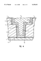
- FIG. 4 is an elevational view of the interconnection structure of FIG. 3 after the copper seed layer is converted into an intermetallic underlayer for the interconnection in accordance with the present invention.
- FIGS. 5a and 5b are elevational views of an alternate embodiment of the invention where the intermetallic layer is formed in the middle of the copper interconnection wherein FIG. 5a shows a small dimension via-stud and FIG. 5b shows a large dimension via-stud.
- FIGS. 6a-d are elevational views of the structure formed as shown in FIG. 3, but with a thin layer of copper removed from the top surface to show the sequence of processing steps to form a cap layer in accordance with the present invention.
- FIGS. 2-6d of the drawings in which like numerals refer to like features of the invention.
- Features of the invention are not necessarily shown to scale in the drawings.
- FIG. 2 there is shown a cross-section of conventional silicon semiconductor structure comprised of various device contact studs 101 and local interconnects 102, typically tungsten with underlayers of titanium and titanium nitride (not shown).
- the method of the present invention forms reliable multilevel interconnections of copper lines, at sub-micron pitch, and isolated from one another by low dielectric insulation, making contacts to electrical features in a substrate.
- the substrate structure may be a semiconductor having plurality of electronic devices, an organic circuit carrier, or a ceramic circuit carrier.
- the local interconnects 102 are preferably formed by damascene methods of prior art, with the top surfaces of the local interconnects being substantially planar with the surface of surrounding insulator 103, typically deposited boro-silicate or phospho-silicate glass or SiO 2 .
- Dielectric insulator layers 2, 3 and 4 are next deposited to begin a process of forming high conductivity interconnections.
- the pair of insulators may be deposited by ECR, sputtering, Plasma Enhanced CVD, CVD, spin-coating or any combination of these methods.
- these insulators may be made of polyimide, silicon-nitride, alumina, silicon-dioxide, phospho-silicate glass, yttrium oxide, magnesium oxide, aero-gel, or any combination of these materials.
- a via-stud pattern is next defined atop insulator 4, for example, by a photolithographic process, followed by the step of etching insulator 4 and partially etching insulator 3 with suitable etchants.
- the pattern for the high conductivity metal interconnection lines is next defined, again, for example, by a photolithographic process, followed by etching remainder of insulator 3 and insulator 2 to form trenches 12 and holes 13 to expose metal line 102.
- liner materials and high conductivity metal of choice are deposited in accordance with the present invention, and polished by chemical-mechanical methods to remove excess metals, thereby simultaneously forming the via-stud and interconnection metal line patterns.
- the present invention is implemented at the point in the process where the combined via-stud and interconnection line patterns are etched in insulator layers 2, 3 and 4 to expose portions of local interconnect 102.
- FIG. 3 where only a portion of FIG. 2 is shown for clarity.
- a thin layer 5 typically 100 to 300 angstroms thick, of an adhesive and contact metal, preferably titanium, tantalum or tantalum nitride.
- an optional thermal diffusion barrier layer 6 typically 200 to 400 angstroms thick, of material such as chromium-chromium oxide, tungsten-silicon, tungsten-nitride, tungsten-nitride-silicon, titanium-nitride, tantalum or tantalum-nitride.
- Layers 5 and 6 are referred to as the liner metallurgy employed in the present invention.
- the contact metal may be, for example, titanium, tantalum or tantalum-nitride, for example.
- the barrier material may be titanium-nitride, titanium-oxy-nitride, tantalum, tantalum-nitride, chromium, chromium/chromium-oxide, tungsten, tungsten-nitride, tungsten-silicon, or any combination among them.
- a thin layer 7 preferably from about 100 to 600 angstroms thick, of an element which is capable of forming an intermetallic compound with copper.
- element may be selected from the group consisting of hafnium, lanthanum, zirconium, tin and titanium.
- a thin copper seed layer 8 typically 600 to 2000 angstroms thick.
- Layers 5-8 may be deposited by common or separate deposition techniques such as sputtering, evaporation or CVD.
- a sputtering technique is employed such as reactive sputtering, collimated sputtering, magnetron sputtering, low pressure sputtering, ECR sputtering, ionized beam sputtering or any combination of them. More preferably, these aforementioned depositions of layers 5, 6, and 7 and 8 are carried out using collimated sputtering in a single pump down and employing the technique for depositing reactive metals taught by Dalal and Lowney in U.S. Pat. No.
- the preferred deposition temperature is between 120°-400° C.
- the copper seed layer also contains carbon in interstitial positions, for enhanced electromigration resistance, and will be discussed further below.
- a remaining layer 9 of copper is then electroplated to fill the trenches.
- layer 9 may be deposited by CVD methods.
- the substrate wafers are then polished by chemical-mechanical methods to remove all excess metals from unpatterned areas, thereby, resulting the planarized structure shown in FIG. 3.
- the substrate wafers are next heated in a non-reactive atmosphere such as nitrogen to a temperature of about 250°-450° C. for 30 min. to 2 hours.
- a non-reactive atmosphere such as nitrogen
- the copper intermetallic layer provides an improved electromigration resistance to the copper layers 8 and 9.
- the thickness of the intermetallic forming metal is preferably selected so as to consume all of the copper seed layer 8 (FIG. 3) during formation of the intermetallic compound.
- the intermetallic compounds formed in the copper layer by the present invention may be hafnium cupride (Hf 2 Cu), lanthanum cupride (LaCu 2 ), eta-bronze (Cu 6 Sn 5 ), titanium cupride (TiCu) and zirconium cupride (Zr 2 Cu).
- the intermetallic layer may be a complete intermetallic or a combination of intermetallic and constituent metal layers.
- the choice of intermetallic forming element may be based on two criteria. First, the chosen element preferably has no, or less than 2 atomic percent, solubility in copper. Low solubility is important as otherwise the element will diffuse into copper and affect its electrical conductivity. Second, the element preferably forms a stable intermetallic with copper. In addition to the above mentioned elements, any other elements which meet these criteria may be employed as the copper intermetallic-forming element.
- the intermetallic layer is formed at the middle of the interconnection thickness, as shown in FIG. 5a for small dimension via studs, and in FIG. 5b for a wider via-stud.
- intermetallic layer 7 is deposited after an initial layer of copper so as to form the intermetallic compound region away from the edges of the copper and toward the interior region.
- FIG. 5a shows the intermetallic region 10 after heat treatment (where the intermetallic element layer 7 was initially deposited) in a Y-shape in the interior of the copper layer 9.
- more than one intermetallic region may be employed, as shown in FIG. 5b where two regions of intermetallic element 7 were deposited in the location where intermetallic compound regions 10a and 10b are shown, after heat treatment.
- the intermetallic forming element is deposited on the top of the copper lines in the form of a cap.
- a thin layer of copper approximately 100 to 400 angstroms thick, is removed to recess its surface from the surrounding insulation surface. Removal may be by light chemical-mechanical polishing, mechanical polishing, or both, of the copper interconnect lines or via-studs to provide a planarized cap surface.
- a thin layer of an intermetallic forming element is next selectively deposited by the aforementioned methods (PVD, electroplating, electroless plating, CVD, or by any combination of them) preferably after in-situ sputter cleaning of the wafer. Excess metal from outside the interconnect trench is then removed by chemical-mechanical polishing, or simply mechanical polishing, leaving the cap of intermetallic forming element atop copper lines at the same level as the surface of layer 4, as shown in FIG. 6c. The next step is to heat treat the wafers, as described above, to form intermetallic compound layer 10 at the top of the copper layer 9. In FIG. 6d there is shown the embodiment where the intermetallic layer or region is formed both at the bottom and at the top of the copper interconnection layer.
- This method of forming an intermetallic cap layer has an advantage of fully covering the copper lines along the line edges, as opposed to leaving narrow slits of copper exposed, as in methods where cap metal is deposited along with the liner and copper. It should be understood that, whereas this method of forming a cap is described here with the objective of forming a cap of an intermetallic compound, the method is not limited to such metals, but any desired metal, alloy or intermetallic compound may be used, such as tungsten, tungsten-silicon, tungsten-nitrogen, hafnium, zirconium, tantalum, tantalum-nitride, titanium, tin, lanthanum, germanium, carbon, chromium, chromium-chromium oxide, platinum, or any combination among them.
- the copper intermetallic layer is formed by selective deposition either at the bottom, in the middle, at the top of the copper line cross-section, or at any combination of these sites.
- the present invention provides a method to form in-situ a copper intermetallic layer at any or all of these regions to improve the electromigration resistance of copper interconnection lines.
- the copper seed layer is preferably deposited in a vacuum tool along with intentional bleeding of a carbonaceous material, in gaseous form.
- the substrate is preferably held at a temperature from about 100-400° C.
- the carbonaceous material is a hydrocarbon that does not contain oxygen, nitrogen or sulphur, such as those carbonaceous material belonging to the C x H y or C x H x hydrocarbon groups.
- the carbonaceous material may be introduced into the vacuum tool in concentrated form, or in a diluted form using an inert carrier gas.
- the vacuum tool is a sputtering or an evaporation tool, and the partial pressure of the carbonaceous material is from about 10 -4 to 10 -7 Torr.
- More preferred parameters of such deposition process are initially pumping down the substrate to a pressure of 10 -8 Torr, bleeding in acetylene gas at a pressure of 10 -5 Torr using an automatic pressure control, and subsequently introducing argon gas at a pressure of 4 in. Torr and sputter depositing the copper into the trenches of the substrate.
- This aspect of the present invention provides an interconnection of copper having 0.1 ppm to 15 ppm dissolved carbon in the copper lattice.
- the copper seed layer 8 is deposited for the purpose of electroplating copper in the next process step. If a choice is made to use CVD copper for layer, seed layer 8 is not needed.
- the pair of insulators could be organic/inorganic, organic/organic or inorganic/inorganic.
Abstract
Description
Claims (13)
Priority Applications (10)
| Application Number | Priority Date | Filing Date | Title |
|---|---|---|---|
| US08/866,777 US6130161A (en) | 1997-05-30 | 1997-05-30 | Method of forming copper interconnections with enhanced electromigration resistance and reduced defect sensitivity |
| US08/947,277 US6069068A (en) | 1997-05-30 | 1997-10-08 | Sub-quarter-micron copper interconnections with improved electromigration resistance and reduced defect sensitivity |
| DE69836114T DE69836114T2 (en) | 1997-05-30 | 1998-05-08 | Copper wiring with improved electromigration resistance and reduced defect sensitivity |
| EP98303611A EP0881673B1 (en) | 1997-05-30 | 1998-05-08 | Copper interconnections with improved electromigration resistance and reduced defect sensitivity |
| JP10143914A JP3057054B2 (en) | 1997-05-30 | 1998-05-26 | Method for forming multilayer interconnect of copper wires |
| TW087108346A TW437044B (en) | 1997-05-30 | 1998-05-28 | Sub-quarter-micron copper interconnections with improved electromigration resistance and reduced defect sensitivity |
| KR1019980020129A KR100304395B1 (en) | 1997-05-30 | 1998-05-30 | Sub-quarter-micron copper interconnections with improved electromigration resistance and reduced defect sensitivity |
| US09/240,950 US6348731B1 (en) | 1997-05-30 | 1999-01-29 | Copper interconnections with enhanced electromigration resistance and reduced defect sensitivity and method of forming same |
| US09/457,960 US6287954B1 (en) | 1997-05-30 | 1999-12-09 | Method of forming copper interconnections with enhanced electromigration resistance and reduced defect sensitivity |
| US09/459,167 US6258710B1 (en) | 1997-05-30 | 1999-12-10 | Sub-quarter-micron copper interconnections with improved electromigration resistance and reduced defect sensitivity |
Applications Claiming Priority (1)
| Application Number | Priority Date | Filing Date | Title |
|---|---|---|---|
| US08/866,777 US6130161A (en) | 1997-05-30 | 1997-05-30 | Method of forming copper interconnections with enhanced electromigration resistance and reduced defect sensitivity |
Related Child Applications (3)
| Application Number | Title | Priority Date | Filing Date |
|---|---|---|---|
| US08/947,277 Continuation-In-Part US6069068A (en) | 1997-05-30 | 1997-10-08 | Sub-quarter-micron copper interconnections with improved electromigration resistance and reduced defect sensitivity |
| US09/240,950 Division US6348731B1 (en) | 1997-05-30 | 1999-01-29 | Copper interconnections with enhanced electromigration resistance and reduced defect sensitivity and method of forming same |
| US09/457,960 Continuation US6287954B1 (en) | 1997-05-30 | 1999-12-09 | Method of forming copper interconnections with enhanced electromigration resistance and reduced defect sensitivity |
Publications (1)
| Publication Number | Publication Date |
|---|---|
| US6130161A true US6130161A (en) | 2000-10-10 |
Family
ID=25348382
Family Applications (3)
| Application Number | Title | Priority Date | Filing Date |
|---|---|---|---|
| US08/866,777 Expired - Lifetime US6130161A (en) | 1997-05-30 | 1997-05-30 | Method of forming copper interconnections with enhanced electromigration resistance and reduced defect sensitivity |
| US09/240,950 Expired - Fee Related US6348731B1 (en) | 1997-05-30 | 1999-01-29 | Copper interconnections with enhanced electromigration resistance and reduced defect sensitivity and method of forming same |
| US09/457,960 Expired - Fee Related US6287954B1 (en) | 1997-05-30 | 1999-12-09 | Method of forming copper interconnections with enhanced electromigration resistance and reduced defect sensitivity |
Family Applications After (2)
| Application Number | Title | Priority Date | Filing Date |
|---|---|---|---|
| US09/240,950 Expired - Fee Related US6348731B1 (en) | 1997-05-30 | 1999-01-29 | Copper interconnections with enhanced electromigration resistance and reduced defect sensitivity and method of forming same |
| US09/457,960 Expired - Fee Related US6287954B1 (en) | 1997-05-30 | 1999-12-09 | Method of forming copper interconnections with enhanced electromigration resistance and reduced defect sensitivity |
Country Status (1)
| Country | Link |
|---|---|
| US (3) | US6130161A (en) |
Cited By (60)
| Publication number | Priority date | Publication date | Assignee | Title |
|---|---|---|---|---|
| US6239021B1 (en) * | 1999-05-24 | 2001-05-29 | Advanced Micro Devices, Inc. | Dual barrier and conductor deposition in a dual damascene process for semiconductors |
| US6258710B1 (en) | 1997-05-30 | 2001-07-10 | International Business Machines Corporation | Sub-quarter-micron copper interconnections with improved electromigration resistance and reduced defect sensitivity |
| US6265746B1 (en) * | 1998-05-28 | 2001-07-24 | Altera Corporation | Highly resistive interconnects |
| US6271136B1 (en) * | 2000-04-04 | 2001-08-07 | Taiwan Semiconductor Manufacturing Company | Multi-step plasma process for forming TiSiN barrier |
| US6287954B1 (en) | 1997-05-30 | 2001-09-11 | International Business Machines Corporation | Method of forming copper interconnections with enhanced electromigration resistance and reduced defect sensitivity |
| US6319834B1 (en) * | 1999-08-18 | 2001-11-20 | Advanced Micro Devices, Inc. | Method and apparatus for improved planarity metallization by electroplating and CMP |
| US6340638B1 (en) * | 2000-03-31 | 2002-01-22 | Taiwan Semiconductor Manufacturing Company, Ltd | Method for forming a passivation layer on copper conductive elements |
| US6362526B1 (en) * | 1998-10-08 | 2002-03-26 | Advanced Micro Devices, Inc. | Alloy barrier layers for semiconductors |
| US6406996B1 (en) * | 2000-09-30 | 2002-06-18 | Advanced Micro Devices, Inc. | Sub-cap and method of manufacture therefor in integrated circuit capping layers |
| US6406997B1 (en) * | 1999-06-09 | 2002-06-18 | Klaus Schroder | Chromium films and chromium film overlayers |
| US6436825B1 (en) * | 2000-04-03 | 2002-08-20 | Taiwan Semiconductor Manufacturing Company | Method of copper barrier layer formation |
| US6461675B2 (en) * | 1998-07-10 | 2002-10-08 | Cvc Products, Inc. | Method for forming a copper film on a substrate |
| US20020170173A1 (en) * | 2001-05-21 | 2002-11-21 | Shinko Electric Industries Co., Ltd. | Method of production of circuit board, semiconductor device, and plating system |
| US20020175423A1 (en) * | 2001-02-08 | 2002-11-28 | Leonard Forbes | High performance silicon contact for flip chip |
| US20020182859A1 (en) * | 2000-01-18 | 2002-12-05 | Micron Technology, Inc. | Structures and methods to enhance copper metallization |
| WO2003001589A2 (en) * | 2001-06-20 | 2003-01-03 | Advanced Micro Devices, Inc. | A method of selectively alloying interconnect regions by depostion process |
| US6528412B1 (en) * | 2001-04-30 | 2003-03-04 | Advanced Micro Devices, Inc. | Depositing an adhesion skin layer and a conformal seed layer to fill an interconnect opening |
| US6538327B1 (en) * | 2000-07-28 | 2003-03-25 | Advanced Micro Devices, Inc. | Method of copper interconnect formation using atomic layer copper deposition and a device thereby formed |
| US6566259B1 (en) * | 1997-12-02 | 2003-05-20 | Applied Materials, Inc. | Integrated deposition process for copper metallization |
| US20030203617A1 (en) * | 2002-04-26 | 2003-10-30 | Michael Lane | Process of forming copper structures |
| US6642145B1 (en) * | 2001-06-04 | 2003-11-04 | Advanced Micro Devices, Inc. | Method of manufacturing an integrated circuit with a dielectric diffusion barrier layer formed between interconnects and interlayer dielectric layers |
| US20030228749A1 (en) * | 2002-06-06 | 2003-12-11 | Nishant Sinha | Plating metal caps on conductive interconnect for wirebonding |
| US6663786B2 (en) * | 2001-06-14 | 2003-12-16 | International Business Machines Corporation | Structure having embedded flush circuitry features and method of fabricating |
| US20040038522A1 (en) * | 1997-06-13 | 2004-02-26 | Ahn Kie Y. | Method of fabricating a semiconductor interconnect structure |
| US6703712B2 (en) * | 2001-11-13 | 2004-03-09 | Agere Systems, Inc. | Microelectronic device layer deposited with multiple electrolytes |
| US20040053446A1 (en) * | 1998-04-17 | 2004-03-18 | Nec Electronics Corporation | Semiconductor device and manufacturing method of the same |
| US6717266B1 (en) * | 2002-06-18 | 2004-04-06 | Advanced Micro Devices, Inc. | Use of an alloying element to form a stable oxide layer on the surface of metal features |
| KR100447232B1 (en) * | 2001-12-28 | 2004-09-04 | 주식회사 하이닉스반도체 | Method for Forming Metal Line in Dual Damascene Structure |
| US6787912B2 (en) * | 2002-04-26 | 2004-09-07 | International Business Machines Corporation | Barrier material for copper structures |
| US20040175926A1 (en) * | 2003-03-07 | 2004-09-09 | Advanced Micro Devices, Inc. | Method for manufacturing a semiconductor component having a barrier-lined opening |
| US20040203227A1 (en) * | 1999-03-29 | 2004-10-14 | Miller Anne E. | Ceric-ion slurry for use in chemical-mechanical polishing |
| US6818546B2 (en) | 2000-05-08 | 2004-11-16 | Renesas Technology Corp. | Semiconductor integrated circuit device and a method of manufacturing the same |
| US6825561B1 (en) | 2003-06-19 | 2004-11-30 | International Business Machines Corporation | Structure and method for eliminating time dependent dielectric breakdown failure of low-k material |
| US20050142865A1 (en) * | 2003-12-31 | 2005-06-30 | Dongbuanam Semiconductor Inc. | Methods of fabricating via hole and trench |
| US20050142833A1 (en) * | 2003-12-30 | 2005-06-30 | Dongbuanam Semiconductor Inc. | Method of fabricating semiconductor device |
| US20050153116A1 (en) * | 2003-12-30 | 2005-07-14 | Dongbuanam Semiconductor Inc. | Method for fabricating semiconductor device |
| US20050161817A1 (en) * | 2004-01-26 | 2005-07-28 | Moritz-Andreas Meyer | Technique for forming embedded metal lines having increased resistance against stress-induced material transport |
| US20050161825A1 (en) * | 2003-03-28 | 2005-07-28 | Fujitsu Limited | Semiconductor device |
| US20060001170A1 (en) * | 2004-07-01 | 2006-01-05 | Fan Zhang | Conductive compound cap layer |
| US20060121734A1 (en) * | 2004-12-03 | 2006-06-08 | Kazuyuki Higashi | Semiconductor device |
| US20070134913A1 (en) * | 2005-12-14 | 2007-06-14 | Semiconductor Manufacturing International (Shanghai) Corporation | Method to eliminate Cu dislocation for reliability and yield |
| US20070164280A1 (en) * | 2003-08-28 | 2007-07-19 | Shinji Maekawa | Thin film transistor, manufacturing method for thin film transistor and manufacturing method for display device |
| CN100334709C (en) * | 2000-11-02 | 2007-08-29 | 富士通株式会社 | Semiconductor device and method of manufacturing the same |
| KR100758886B1 (en) * | 2001-04-27 | 2007-09-19 | 후지쯔 가부시끼가이샤 | Semiconductor device and method of manufacturing the same |
| US7273808B1 (en) | 2003-02-03 | 2007-09-25 | Novellus Systems, Inc. | Reactive barrier/seed preclean process for damascene process |
| US20070269978A1 (en) * | 2006-05-18 | 2007-11-22 | Chien-Hsueh Shih | Process for improving copper line cap formation |
| US7456501B1 (en) * | 1998-01-20 | 2008-11-25 | International Business Machines Corporation | Semiconductor structure having recess with conductive metal |
| US7504674B2 (en) * | 2003-08-05 | 2009-03-17 | Micron Technology, Inc. | Electronic apparatus having a core conductive structure within an insulating layer |
| US20100025857A1 (en) * | 2008-07-29 | 2010-02-04 | Lindgren Peter J | Ic chip and design structure with through wafer vias dishing correction |
| US20100029075A1 (en) * | 2008-07-29 | 2010-02-04 | Lindgren Peter J | Through wafer vias with dishing correction methods |
| CN1360346B (en) * | 2000-12-18 | 2010-05-26 | 国际商业机器公司 | Electronic structure and forming method thereof |
| CN101459121B (en) * | 2007-12-13 | 2010-06-09 | 中芯国际集成电路制造(上海)有限公司 | Through hole and through hole forming method |
| US7745934B2 (en) | 2000-01-18 | 2010-06-29 | Micron Technology, Inc. | Integrated circuit and seed layers |
| US20120126415A1 (en) * | 2010-11-18 | 2012-05-24 | Shai Haimson | Filling Cavities in Semiconductor Structures |
| CN103839604A (en) * | 2014-02-26 | 2014-06-04 | 京东方科技集团股份有限公司 | Heat conducting film, manufacturing method of heat conducting film, and array substrate |
| US20140327141A1 (en) * | 2012-04-13 | 2014-11-06 | Taiwan Semiconductor Manufacturing Company, Ltd. | Copper interconnect structure and method for forming the same |
| US20170194229A1 (en) * | 2015-12-30 | 2017-07-06 | Globalfoundries Singapore Pte. Ltd. | Integrated circuits with aluminum via structures and methods for fabricating the same |
| US20180005939A1 (en) * | 2016-06-30 | 2018-01-04 | International Business Machines Corporation | Techniques to Improve Reliability in Cu Interconnects Using Cu Intermetallics |
| US20200219759A1 (en) * | 2018-10-04 | 2020-07-09 | International Business Machines Corporation | Back end of line integration for interconnects |
| US11152317B2 (en) | 2018-09-20 | 2021-10-19 | Samsung Electronics Co., Ltd. | Semiconductor device including interconnection structure including copper and tin and semiconductor package including the same |
Families Citing this family (38)
| Publication number | Priority date | Publication date | Assignee | Title |
|---|---|---|---|---|
| US6429120B1 (en) | 2000-01-18 | 2002-08-06 | Micron Technology, Inc. | Methods and apparatus for making integrated-circuit wiring from copper, silver, gold, and other metals |
| KR100635685B1 (en) * | 1998-05-25 | 2006-10-17 | 가부시키가이샤 히타치세이사쿠쇼 | Semiconductor equipment and fabrication method thereof |
| JP3708732B2 (en) | 1998-12-25 | 2005-10-19 | Necエレクトロニクス株式会社 | Manufacturing method of semiconductor device |
| US6228687B1 (en) * | 1999-06-28 | 2001-05-08 | Micron Technology, Inc. | Wafer-level package and methods of fabricating |
| US6433429B1 (en) * | 1999-09-01 | 2002-08-13 | International Business Machines Corporation | Copper conductive line with redundant liner and method of making |
| US7388289B1 (en) * | 1999-09-02 | 2008-06-17 | Micron Technology, Inc. | Local multilayered metallization |
| JP3329380B2 (en) * | 1999-09-21 | 2002-09-30 | 日本電気株式会社 | Semiconductor device and method of manufacturing the same |
| US6221780B1 (en) * | 1999-09-29 | 2001-04-24 | International Business Machines Corporation | Dual damascene flowable oxide insulation structure and metallic barrier |
| US6569751B1 (en) * | 2000-07-17 | 2003-05-27 | Lsi Logic Corporation | Low via resistance system |
| US6710452B1 (en) * | 2000-07-19 | 2004-03-23 | Advanced Micro Devices, Inc. | Coherent diffusion barriers for integrated circuit interconnects |
| KR100351933B1 (en) * | 2000-08-28 | 2002-09-12 | 삼성전자 주식회사 | Method of forming a contact structure in semiconductor device |
| US6566248B1 (en) * | 2001-01-11 | 2003-05-20 | Advanced Micro Devices, Inc. | Graphoepitaxial conductor cores in integrated circuit interconnects |
| JP2002217292A (en) * | 2001-01-23 | 2002-08-02 | Hitachi Ltd | Semiconductor integrated circuit device and its manufacturing method |
| KR100499557B1 (en) * | 2001-06-11 | 2005-07-07 | 주식회사 하이닉스반도체 | method for fabricating the wire of semiconductor device |
| US6544891B1 (en) * | 2001-09-04 | 2003-04-08 | Taiwan Semiconductor Manufacturing Company | Method to eliminate post-CMP copper flake defect |
| JP2003160877A (en) * | 2001-11-28 | 2003-06-06 | Hitachi Ltd | Method and apparatus for manufacturing semiconductor device |
| JP2003188254A (en) * | 2001-12-18 | 2003-07-04 | Hitachi Ltd | Semiconductor device and manufacturing method therefor |
| US7423336B2 (en) * | 2002-04-08 | 2008-09-09 | Micron Technology, Inc. | Bond pad rerouting element, rerouted semiconductor devices including the rerouting element, and assemblies including the rerouted semiconductor devices |
| US6716744B2 (en) * | 2002-05-06 | 2004-04-06 | Sharp Laboratories Of America, Inc. | Ultra thin tungsten metal films used as adhesion promoter between barrier metals and copper |
| US6849173B1 (en) | 2002-06-12 | 2005-02-01 | Taiwan Semiconductor Manufacturing Company, Ltd. | Technique to enhance the yield of copper interconnections |
| US6800938B2 (en) * | 2002-08-08 | 2004-10-05 | International Business Machines Corporation | Semiconductor device having amorphous barrier layer for copper metallurgy |
| US7279423B2 (en) * | 2002-10-31 | 2007-10-09 | Intel Corporation | Forming a copper diffusion barrier |
| US6975032B2 (en) * | 2002-12-16 | 2005-12-13 | International Business Machines Corporation | Copper recess process with application to selective capping and electroless plating |
| US6884338B2 (en) * | 2002-12-16 | 2005-04-26 | 3M Innovative Properties Company | Methods for polishing and/or cleaning copper interconnects and/or film and compositions therefor |
| US6858124B2 (en) * | 2002-12-16 | 2005-02-22 | 3M Innovative Properties Company | Methods for polishing and/or cleaning copper interconnects and/or film and compositions therefor |
| US7147767B2 (en) * | 2002-12-16 | 2006-12-12 | 3M Innovative Properties Company | Plating solutions for electrochemical or chemical deposition of copper interconnects and methods therefor |
| US7566964B2 (en) * | 2003-04-10 | 2009-07-28 | Agere Systems Inc. | Aluminum pad power bus and signal routing for integrated circuit devices utilizing copper technology interconnect structures |
| EP1680028B1 (en) * | 2003-10-17 | 2012-01-25 | Tyco Healthcare Group LP | Surgical stapling device |
| US7176128B2 (en) * | 2004-01-12 | 2007-02-13 | Infineon Technologies Ag | Method for fabrication of a contact structure |
| US7795150B2 (en) * | 2004-11-29 | 2010-09-14 | Renesas Electronics America Inc. | Metal capping of damascene structures to improve reliability using hyper selective chemical-mechanical deposition |
| US7884477B2 (en) * | 2007-12-03 | 2011-02-08 | International Business Machines Corporation | Air gap structure having protective metal silicide pads on a metal feature |
| US7732922B2 (en) * | 2008-01-07 | 2010-06-08 | International Business Machines Corporation | Simultaneous grain modulation for BEOL applications |
| US20110127673A1 (en) * | 2009-12-01 | 2011-06-02 | International Business Machines Corporation | Wiring structure and method |
| US8872341B2 (en) * | 2010-09-29 | 2014-10-28 | Infineon Technologies Ag | Semiconductor structure having metal oxide or nirtride passivation layer on fill layer and method for making same |
| US8569888B2 (en) | 2011-05-24 | 2013-10-29 | International Business Machines Corporation | Wiring structure and method of forming the structure |
| CN113725156A (en) * | 2011-11-04 | 2021-11-30 | 英特尔公司 | Method and apparatus for forming self-aligned caps |
| CN105355620B (en) * | 2015-12-17 | 2018-06-22 | 上海集成电路研发中心有限公司 | A kind of copper interconnection structure and its manufacturing method |
| US9721889B1 (en) * | 2016-07-26 | 2017-08-01 | Globalfoundries Inc. | Middle of the line (MOL) metal contacts |
Citations (20)
| Publication number | Priority date | Publication date | Assignee | Title |
|---|---|---|---|---|
| US4007039A (en) * | 1975-03-17 | 1977-02-08 | Olin Corporation | Copper base alloys with high strength and high electrical conductivity |
| US4017890A (en) * | 1975-10-24 | 1977-04-12 | International Business Machines Corporation | Intermetallic compound layer in thin films for improved electromigration resistance |
| US4379832A (en) * | 1981-08-31 | 1983-04-12 | International Business Machines Corporation | Method for making low barrier Schottky devices of the electron beam evaporation of reactive metals |
| US4406858A (en) * | 1981-12-30 | 1983-09-27 | General Electric Company | Copper-base alloys containing strengthening and ductilizing amounts of hafnium and zirconium and method |
| US4789648A (en) * | 1985-10-28 | 1988-12-06 | International Business Machines Corporation | Method for producing coplanar multi-level metal/insulator films on a substrate and for forming patterned conductive lines simultaneously with stud vias |
| US4872048A (en) * | 1985-09-13 | 1989-10-03 | Mitsubishi Kinzoku Kabushiki Kaisha | Semiconductor device having copper alloy leads |
| US4985750A (en) * | 1986-09-17 | 1991-01-15 | Fujitsu Limited | Semiconductor device using copper metallization |
| US5187300A (en) * | 1991-02-04 | 1993-02-16 | Air Products And Chemicals, Inc. | Volatile precursors for copper CVD |
| US5252516A (en) * | 1992-02-20 | 1993-10-12 | International Business Machines Corporation | Method for producing interlevel stud vias |
| US5300813A (en) * | 1992-02-26 | 1994-04-05 | International Business Machines Corporation | Refractory metal capped low resistivity metal conductor lines and vias |
| US5312509A (en) * | 1990-04-30 | 1994-05-17 | International Business Machines Corporation | Manufacturing system for low temperature chemical vapor deposition of high purity metals |
| US5322712A (en) * | 1993-05-18 | 1994-06-21 | Air Products And Chemicals, Inc. | Process for improved quality of CVD copper films |
| US5391517A (en) * | 1993-09-13 | 1995-02-21 | Motorola Inc. | Process for forming copper interconnect structure |
| US5414301A (en) * | 1985-03-15 | 1995-05-09 | National Semiconductor Corporation | High temperature interconnect system for an integrated circuit |
| US5434451A (en) * | 1993-01-19 | 1995-07-18 | International Business Machines Corporation | Tungsten liner process for simultaneous formation of integral contact studs and interconnect lines |
| US5470789A (en) * | 1993-03-19 | 1995-11-28 | Fujitsu Limited | Process for fabricating integrated circuit devices |
| US5527739A (en) * | 1993-12-23 | 1996-06-18 | Motorola, Inc. | Process for fabricating a semiconductor device having an improved metal interconnect structure |
| US5539256A (en) * | 1994-02-24 | 1996-07-23 | Nec Corporation | Semiconductor device having an interconnection of a laminate structure and a method for manufacturing the same |
| US5565707A (en) * | 1994-10-31 | 1996-10-15 | International Business Machines Corporation | Interconnect structure using a Al2 Cu for an integrated circuit chip |
| US5656860A (en) * | 1995-04-01 | 1997-08-12 | Lg Semicon Co., Ltd. | Wiring structure for semiconductor device and fabrication method therefor |
Family Cites Families (24)
| Publication number | Priority date | Publication date | Assignee | Title |
|---|---|---|---|---|
| US4153518A (en) | 1977-11-18 | 1979-05-08 | Tektronix, Inc. | Method of making a metalized substrate having a thin film barrier layer |
| US5250329A (en) | 1989-04-06 | 1993-10-05 | Microelectronics And Computer Technology Corporation | Method of depositing conductive lines on a dielectric |
| US5071714A (en) * | 1989-04-17 | 1991-12-10 | International Business Machines Corporation | Multilayered intermetallic connection for semiconductor devices |
| US5256565A (en) | 1989-05-08 | 1993-10-26 | The United States Of America As Represented By The United States Department Of Energy | Electrochemical planarization |
| JPH03244126A (en) | 1990-02-22 | 1991-10-30 | Toshiba Corp | Manufacture of semiconductor device |
| US5273775A (en) | 1990-09-12 | 1993-12-28 | Air Products And Chemicals, Inc. | Process for selectively depositing copper aluminum alloy onto a substrate |
| US5266446A (en) | 1990-11-15 | 1993-11-30 | International Business Machines Corporation | Method of making a multilayer thin film structure |
| JP2811126B2 (en) * | 1991-05-02 | 1998-10-15 | 三菱電機株式会社 | Wiring connection structure of semiconductor integrated circuit device and method of manufacturing the same |
| US5231751A (en) | 1991-10-29 | 1993-08-03 | International Business Machines Corporation | Process for thin film interconnect |
| US5380546A (en) | 1993-06-09 | 1995-01-10 | Microelectronics And Computer Technology Corporation | Multilevel metallization process for electronic components |
| JP3341401B2 (en) | 1993-10-22 | 2002-11-05 | 松下電器産業株式会社 | Method of forming wiring metal film by plating method |
| FR2716197B1 (en) | 1994-02-17 | 1996-04-19 | Adir | New acronymin analogues, process for their preparation and pharmaceutical compositions containing them. |
| JP3517802B2 (en) | 1995-09-01 | 2004-04-12 | 富士通株式会社 | Method of forming buried conductive layer |
| JP3323055B2 (en) * | 1996-04-03 | 2002-09-09 | 株式会社東芝 | Semiconductor device and manufacturing method thereof |
| US5814557A (en) | 1996-05-20 | 1998-09-29 | Motorola, Inc. | Method of forming an interconnect structure |
| US5943601A (en) * | 1997-04-30 | 1999-08-24 | International Business Machines Corporation | Process for fabricating a metallization structure |
| US5899738A (en) * | 1997-05-23 | 1999-05-04 | Taiwan Semiconductor Manufacturing Company, Ltd. | Method for making metal plugs in stacked vias for multilevel interconnections and contact openings while retaining the alignment marks without requiring extra masking steps |
| US6069068A (en) * | 1997-05-30 | 2000-05-30 | International Business Machines Corporation | Sub-quarter-micron copper interconnections with improved electromigration resistance and reduced defect sensitivity |
| US6130161A (en) | 1997-05-30 | 2000-10-10 | International Business Machines Corporation | Method of forming copper interconnections with enhanced electromigration resistance and reduced defect sensitivity |
| US5821168A (en) | 1997-07-16 | 1998-10-13 | Motorola, Inc. | Process for forming a semiconductor device |
| US5897375A (en) | 1997-10-20 | 1999-04-27 | Motorola, Inc. | Chemical mechanical polishing (CMP) slurry for copper and method of use in integrated circuit manufacture |
| US6047499A (en) | 1997-11-04 | 2000-04-11 | Staas; Harry John | Plant saucer with overflow relief valve |
| US6074499A (en) | 1998-01-09 | 2000-06-13 | South Dakoga School Of Mines And Technology | Boron-copper-magnesium-tin alloy and method for making same |
| US6083840A (en) * | 1998-11-25 | 2000-07-04 | Arch Specialty Chemicals, Inc. | Slurry compositions and method for the chemical-mechanical polishing of copper and copper alloys |
-
1997
- 1997-05-30 US US08/866,777 patent/US6130161A/en not_active Expired - Lifetime
-
1999
- 1999-01-29 US US09/240,950 patent/US6348731B1/en not_active Expired - Fee Related
- 1999-12-09 US US09/457,960 patent/US6287954B1/en not_active Expired - Fee Related
Patent Citations (23)
| Publication number | Priority date | Publication date | Assignee | Title |
|---|---|---|---|---|
| US4007039A (en) * | 1975-03-17 | 1977-02-08 | Olin Corporation | Copper base alloys with high strength and high electrical conductivity |
| US4017890A (en) * | 1975-10-24 | 1977-04-12 | International Business Machines Corporation | Intermetallic compound layer in thin films for improved electromigration resistance |
| US4154874A (en) * | 1975-10-24 | 1979-05-15 | International Business Machines Corporation | Method for forming intermetallic layers in thin films for improved electromigration resistance |
| US4379832A (en) * | 1981-08-31 | 1983-04-12 | International Business Machines Corporation | Method for making low barrier Schottky devices of the electron beam evaporation of reactive metals |
| US4406858A (en) * | 1981-12-30 | 1983-09-27 | General Electric Company | Copper-base alloys containing strengthening and ductilizing amounts of hafnium and zirconium and method |
| US5414301A (en) * | 1985-03-15 | 1995-05-09 | National Semiconductor Corporation | High temperature interconnect system for an integrated circuit |
| US4872048A (en) * | 1985-09-13 | 1989-10-03 | Mitsubishi Kinzoku Kabushiki Kaisha | Semiconductor device having copper alloy leads |
| US4789648A (en) * | 1985-10-28 | 1988-12-06 | International Business Machines Corporation | Method for producing coplanar multi-level metal/insulator films on a substrate and for forming patterned conductive lines simultaneously with stud vias |
| US4985750A (en) * | 1986-09-17 | 1991-01-15 | Fujitsu Limited | Semiconductor device using copper metallization |
| US5312509A (en) * | 1990-04-30 | 1994-05-17 | International Business Machines Corporation | Manufacturing system for low temperature chemical vapor deposition of high purity metals |
| US5187300A (en) * | 1991-02-04 | 1993-02-16 | Air Products And Chemicals, Inc. | Volatile precursors for copper CVD |
| US5252516A (en) * | 1992-02-20 | 1993-10-12 | International Business Machines Corporation | Method for producing interlevel stud vias |
| US5403779A (en) * | 1992-02-26 | 1995-04-04 | International Business Machines Corporation | Refractory metal capped low resistivity metal conductor lines and vias formed using PVD and CVD |
| US5300813A (en) * | 1992-02-26 | 1994-04-05 | International Business Machines Corporation | Refractory metal capped low resistivity metal conductor lines and vias |
| US5426330A (en) * | 1992-02-26 | 1995-06-20 | International Business Machines Corporation | Refractory metal capped low resistivity metal conductor lines and vias |
| US5434451A (en) * | 1993-01-19 | 1995-07-18 | International Business Machines Corporation | Tungsten liner process for simultaneous formation of integral contact studs and interconnect lines |
| US5470789A (en) * | 1993-03-19 | 1995-11-28 | Fujitsu Limited | Process for fabricating integrated circuit devices |
| US5322712A (en) * | 1993-05-18 | 1994-06-21 | Air Products And Chemicals, Inc. | Process for improved quality of CVD copper films |
| US5391517A (en) * | 1993-09-13 | 1995-02-21 | Motorola Inc. | Process for forming copper interconnect structure |
| US5527739A (en) * | 1993-12-23 | 1996-06-18 | Motorola, Inc. | Process for fabricating a semiconductor device having an improved metal interconnect structure |
| US5539256A (en) * | 1994-02-24 | 1996-07-23 | Nec Corporation | Semiconductor device having an interconnection of a laminate structure and a method for manufacturing the same |
| US5565707A (en) * | 1994-10-31 | 1996-10-15 | International Business Machines Corporation | Interconnect structure using a Al2 Cu for an integrated circuit chip |
| US5656860A (en) * | 1995-04-01 | 1997-08-12 | Lg Semicon Co., Ltd. | Wiring structure for semiconductor device and fabrication method therefor |
Non-Patent Citations (3)
| Title |
|---|
| IBM Technical Disclosure Bulletin, Optimum Metal Line Structures for Memory Array and Support Circuits, vol. 30, No. 12; May, 1988. * |
| VLSI Multilevel Interconnection Conference (VMIC) ,Planar Copper Polyimide Back End of the Line Interconnections for ULSI Devices, by Luther et al.; pp. 15 21, 1993. * |
| VLSI Multilevel Interconnection Conference (VMIC) ,Planar Copper-Polyimide Back End of the Line Interconnections for ULSI Devices, by Luther et al.; pp. 15-21, 1993. |
Cited By (107)
| Publication number | Priority date | Publication date | Assignee | Title |
|---|---|---|---|---|
| US6258710B1 (en) | 1997-05-30 | 2001-07-10 | International Business Machines Corporation | Sub-quarter-micron copper interconnections with improved electromigration resistance and reduced defect sensitivity |
| US6287954B1 (en) | 1997-05-30 | 2001-09-11 | International Business Machines Corporation | Method of forming copper interconnections with enhanced electromigration resistance and reduced defect sensitivity |
| US6348731B1 (en) | 1997-05-30 | 2002-02-19 | International Business Machines Corporation | Copper interconnections with enhanced electromigration resistance and reduced defect sensitivity and method of forming same |
| US7271085B2 (en) * | 1997-06-13 | 2007-09-18 | Micron Technology, Inc. | Method of fabricating a semiconductor interconnect structure |
| US20040038522A1 (en) * | 1997-06-13 | 2004-02-26 | Ahn Kie Y. | Method of fabricating a semiconductor interconnect structure |
| US6566259B1 (en) * | 1997-12-02 | 2003-05-20 | Applied Materials, Inc. | Integrated deposition process for copper metallization |
| US20030194863A1 (en) * | 1997-12-02 | 2003-10-16 | Applied Materials, Inc. | Integrated deposition process for copper metallization |
| US6881673B2 (en) | 1997-12-02 | 2005-04-19 | Applied Materials, Inc. | Integrated deposition process for copper metallization |
| US7456501B1 (en) * | 1998-01-20 | 2008-11-25 | International Business Machines Corporation | Semiconductor structure having recess with conductive metal |
| US20040053446A1 (en) * | 1998-04-17 | 2004-03-18 | Nec Electronics Corporation | Semiconductor device and manufacturing method of the same |
| US6890852B2 (en) | 1998-04-17 | 2005-05-10 | Nec Electronics Corporation | Semiconductor device and manufacturing method of the same |
| US6265746B1 (en) * | 1998-05-28 | 2001-07-24 | Altera Corporation | Highly resistive interconnects |
| US6461675B2 (en) * | 1998-07-10 | 2002-10-08 | Cvc Products, Inc. | Method for forming a copper film on a substrate |
| US6362526B1 (en) * | 1998-10-08 | 2002-03-26 | Advanced Micro Devices, Inc. | Alloy barrier layers for semiconductors |
| US20040203227A1 (en) * | 1999-03-29 | 2004-10-14 | Miller Anne E. | Ceric-ion slurry for use in chemical-mechanical polishing |
| US6239021B1 (en) * | 1999-05-24 | 2001-05-29 | Advanced Micro Devices, Inc. | Dual barrier and conductor deposition in a dual damascene process for semiconductors |
| US6406997B1 (en) * | 1999-06-09 | 2002-06-18 | Klaus Schroder | Chromium films and chromium film overlayers |
| US6319834B1 (en) * | 1999-08-18 | 2001-11-20 | Advanced Micro Devices, Inc. | Method and apparatus for improved planarity metallization by electroplating and CMP |
| US20020182859A1 (en) * | 2000-01-18 | 2002-12-05 | Micron Technology, Inc. | Structures and methods to enhance copper metallization |
| US7745934B2 (en) | 2000-01-18 | 2010-06-29 | Micron Technology, Inc. | Integrated circuit and seed layers |
| US8779596B2 (en) | 2000-01-18 | 2014-07-15 | Micron Technology, Inc. | Structures and methods to enhance copper metallization |
| US6340638B1 (en) * | 2000-03-31 | 2002-01-22 | Taiwan Semiconductor Manufacturing Company, Ltd | Method for forming a passivation layer on copper conductive elements |
| US6436825B1 (en) * | 2000-04-03 | 2002-08-20 | Taiwan Semiconductor Manufacturing Company | Method of copper barrier layer formation |
| US6271136B1 (en) * | 2000-04-04 | 2001-08-07 | Taiwan Semiconductor Manufacturing Company | Multi-step plasma process for forming TiSiN barrier |
| US20050095844A1 (en) * | 2000-05-08 | 2005-05-05 | Tatsuyuki Saito | Semiconductor integrated circuit device |
| US7321171B2 (en) | 2000-05-08 | 2008-01-22 | Renesas Technology Corp. | Semiconductor integrated circuit device |
| US20080042282A1 (en) * | 2000-05-08 | 2008-02-21 | Tatsuyuki Saito | Semiconductor integrated circuit device and a method of manufacturing the same |
| US6818546B2 (en) | 2000-05-08 | 2004-11-16 | Renesas Technology Corp. | Semiconductor integrated circuit device and a method of manufacturing the same |
| US7642652B2 (en) | 2000-05-08 | 2010-01-05 | Renesas Technology Corp. | Semiconductor integrated circuit device and a method of manufacturing the same |
| US6538327B1 (en) * | 2000-07-28 | 2003-03-25 | Advanced Micro Devices, Inc. | Method of copper interconnect formation using atomic layer copper deposition and a device thereby formed |
| US6515367B1 (en) * | 2000-09-30 | 2003-02-04 | Advanced Micro Devices, Inc. | Sub-cap and method of manufacture therefor in integrated circuit capping layers |
| US6406996B1 (en) * | 2000-09-30 | 2002-06-18 | Advanced Micro Devices, Inc. | Sub-cap and method of manufacture therefor in integrated circuit capping layers |
| CN100334709C (en) * | 2000-11-02 | 2007-08-29 | 富士通株式会社 | Semiconductor device and method of manufacturing the same |
| CN1360346B (en) * | 2000-12-18 | 2010-05-26 | 国际商业机器公司 | Electronic structure and forming method thereof |
| US6737740B2 (en) * | 2001-02-08 | 2004-05-18 | Micron Technology, Inc. | High performance silicon contact for flip chip |
| US6812137B2 (en) | 2001-02-08 | 2004-11-02 | Micron Technology, Inc. | Method of forming coaxial integrated circuitry interconnect lines |
| US20030207566A1 (en) * | 2001-02-08 | 2003-11-06 | Leonard Forbes | High performance silicon contact for flip chip |
| US6828656B2 (en) | 2001-02-08 | 2004-12-07 | Micron Technology, Inc. | High performance silicon contact for flip chip and a system using same |
| US20020175423A1 (en) * | 2001-02-08 | 2002-11-28 | Leonard Forbes | High performance silicon contact for flip chip |
| KR100758886B1 (en) * | 2001-04-27 | 2007-09-19 | 후지쯔 가부시끼가이샤 | Semiconductor device and method of manufacturing the same |
| US6528412B1 (en) * | 2001-04-30 | 2003-03-04 | Advanced Micro Devices, Inc. | Depositing an adhesion skin layer and a conformal seed layer to fill an interconnect opening |
| US20020170173A1 (en) * | 2001-05-21 | 2002-11-21 | Shinko Electric Industries Co., Ltd. | Method of production of circuit board, semiconductor device, and plating system |
| US7114251B2 (en) * | 2001-05-21 | 2006-10-03 | Shinko Electric Industries Co., Ltd. | Method of producing of circuit board; for semiconductor device |
| US6642145B1 (en) * | 2001-06-04 | 2003-11-04 | Advanced Micro Devices, Inc. | Method of manufacturing an integrated circuit with a dielectric diffusion barrier layer formed between interconnects and interlayer dielectric layers |
| US6663786B2 (en) * | 2001-06-14 | 2003-12-16 | International Business Machines Corporation | Structure having embedded flush circuitry features and method of fabricating |
| US6841228B2 (en) * | 2001-06-14 | 2005-01-11 | International Business Machines Corporation | Structure having embedded flush circuitry features and method of fabricating |
| WO2003001589A2 (en) * | 2001-06-20 | 2003-01-03 | Advanced Micro Devices, Inc. | A method of selectively alloying interconnect regions by depostion process |
| US6656834B1 (en) | 2001-06-20 | 2003-12-02 | Advanced Micro Devices, Inc. | Method of selectively alloying interconnect regions by deposition process |
| WO2003001589A3 (en) * | 2001-06-20 | 2003-03-20 | Advanced Micro Devices Inc | A method of selectively alloying interconnect regions by depostion process |
| US6703712B2 (en) * | 2001-11-13 | 2004-03-09 | Agere Systems, Inc. | Microelectronic device layer deposited with multiple electrolytes |
| KR100447232B1 (en) * | 2001-12-28 | 2004-09-04 | 주식회사 하이닉스반도체 | Method for Forming Metal Line in Dual Damascene Structure |
| US20030203617A1 (en) * | 2002-04-26 | 2003-10-30 | Michael Lane | Process of forming copper structures |
| US6787912B2 (en) * | 2002-04-26 | 2004-09-07 | International Business Machines Corporation | Barrier material for copper structures |
| US20040157433A1 (en) * | 2002-06-06 | 2004-08-12 | Nishant Sinha | Plating metal caps on conductive interconnect for wirebonding |
| US20030228749A1 (en) * | 2002-06-06 | 2003-12-11 | Nishant Sinha | Plating metal caps on conductive interconnect for wirebonding |
| US6717266B1 (en) * | 2002-06-18 | 2004-04-06 | Advanced Micro Devices, Inc. | Use of an alloying element to form a stable oxide layer on the surface of metal features |
| US7273808B1 (en) | 2003-02-03 | 2007-09-25 | Novellus Systems, Inc. | Reactive barrier/seed preclean process for damascene process |
| US20040175926A1 (en) * | 2003-03-07 | 2004-09-09 | Advanced Micro Devices, Inc. | Method for manufacturing a semiconductor component having a barrier-lined opening |
| US20050161825A1 (en) * | 2003-03-28 | 2005-07-28 | Fujitsu Limited | Semiconductor device |
| US7923806B2 (en) | 2003-03-28 | 2011-04-12 | Fujitsu Semiconductor Limited | Embedded wiring in copper damascene with void suppressing structure |
| US20040256729A1 (en) * | 2003-06-19 | 2004-12-23 | International Business Machines Corporation | Structure and method for eliminating time dependent dielectric breakdown failure of low-k material |
| US6825561B1 (en) | 2003-06-19 | 2004-11-30 | International Business Machines Corporation | Structure and method for eliminating time dependent dielectric breakdown failure of low-k material |
| US7504674B2 (en) * | 2003-08-05 | 2009-03-17 | Micron Technology, Inc. | Electronic apparatus having a core conductive structure within an insulating layer |
| US20070164280A1 (en) * | 2003-08-28 | 2007-07-19 | Shinji Maekawa | Thin film transistor, manufacturing method for thin film transistor and manufacturing method for display device |
| US7256122B2 (en) * | 2003-12-30 | 2007-08-14 | Dongbu Electronics Co., Ltd. | Method of fabricating semiconductor device |
| US20050153116A1 (en) * | 2003-12-30 | 2005-07-14 | Dongbuanam Semiconductor Inc. | Method for fabricating semiconductor device |
| US7098134B2 (en) | 2003-12-30 | 2006-08-29 | Dongbu Electronics Co., Ltd. | Method for fabricating semiconductor device |
| US20050142833A1 (en) * | 2003-12-30 | 2005-06-30 | Dongbuanam Semiconductor Inc. | Method of fabricating semiconductor device |
| US7297630B2 (en) | 2003-12-31 | 2007-11-20 | Dongbu Electronics Co., Ltd. | Methods of fabricating via hole and trench |
| US20050142865A1 (en) * | 2003-12-31 | 2005-06-30 | Dongbuanam Semiconductor Inc. | Methods of fabricating via hole and trench |
| US20050161817A1 (en) * | 2004-01-26 | 2005-07-28 | Moritz-Andreas Meyer | Technique for forming embedded metal lines having increased resistance against stress-induced material transport |
| DE102004003863A1 (en) * | 2004-01-26 | 2005-08-18 | Advanced Micro Devices, Inc., Sunnyvale | Technique for making embedded metal lines with increased resistance to stress-induced material transport |
| DE102004003863B4 (en) * | 2004-01-26 | 2009-01-29 | Advanced Micro Devices, Inc., Sunnyvale | Technique for making embedded metal lines with increased resistance to stress-induced material transport |
| US8039395B2 (en) | 2004-01-26 | 2011-10-18 | Globalfoundries Inc. | Technique for forming embedded metal lines having increased resistance against stress-induced material transport |
| US20060001170A1 (en) * | 2004-07-01 | 2006-01-05 | Fan Zhang | Conductive compound cap layer |
| US20060121734A1 (en) * | 2004-12-03 | 2006-06-08 | Kazuyuki Higashi | Semiconductor device |
| US7422977B2 (en) * | 2004-12-03 | 2008-09-09 | Kabushiki Kaisha Toshiba | Copper adhesion improvement device and method |
| US20070134913A1 (en) * | 2005-12-14 | 2007-06-14 | Semiconductor Manufacturing International (Shanghai) Corporation | Method to eliminate Cu dislocation for reliability and yield |
| US7897508B2 (en) * | 2005-12-14 | 2011-03-01 | Semiconductor Manufacturing International (Shanghai) Corporation | Method to eliminate Cu dislocation for reliability and yield |
| US8193087B2 (en) | 2006-05-18 | 2012-06-05 | Taiwan Semiconductor Manufacturing Co., Ltd. | Process for improving copper line cap formation |
| US20070269978A1 (en) * | 2006-05-18 | 2007-11-22 | Chien-Hsueh Shih | Process for improving copper line cap formation |
| US8623760B2 (en) | 2006-05-18 | 2014-01-07 | Taiwan Semiconductor Manufacturing Company, Ltd. | Process for improving copper line cap formation |
| CN101459121B (en) * | 2007-12-13 | 2010-06-09 | 中芯国际集成电路制造(上海)有限公司 | Through hole and through hole forming method |
| US20120137515A1 (en) * | 2008-07-29 | 2012-06-07 | International Business Machines Corporation | Through wafer vias with dishing correction methods |
| US8166651B2 (en) * | 2008-07-29 | 2012-05-01 | International Business Machines Corporation | Through wafer vias with dishing correction methods |
| US20100029075A1 (en) * | 2008-07-29 | 2010-02-04 | Lindgren Peter J | Through wafer vias with dishing correction methods |
| US8631570B2 (en) * | 2008-07-29 | 2014-01-21 | International Business Machines Corporation | Through wafer vias with dishing correction methods |
| US20100025857A1 (en) * | 2008-07-29 | 2010-02-04 | Lindgren Peter J | Ic chip and design structure with through wafer vias dishing correction |
| US7859114B2 (en) | 2008-07-29 | 2010-12-28 | International Business Machines Corporation | IC chip and design structure with through wafer vias dishing correction |
| US20120126415A1 (en) * | 2010-11-18 | 2012-05-24 | Shai Haimson | Filling Cavities in Semiconductor Structures |
| US8772155B2 (en) * | 2010-11-18 | 2014-07-08 | Micron Technology, Inc. | Filling cavities in semiconductor structures having adhesion promoting layer in the cavities |
| US9159662B2 (en) | 2010-11-18 | 2015-10-13 | Micron Technology, Inc. | Semiconductor structures having adhesion promoting layer in cavities |
| US9142509B2 (en) * | 2012-04-13 | 2015-09-22 | Taiwan Semiconductor Manufacturing Company, Ltd. | Copper interconnect structure and method for forming the same |
| US20140327141A1 (en) * | 2012-04-13 | 2014-11-06 | Taiwan Semiconductor Manufacturing Company, Ltd. | Copper interconnect structure and method for forming the same |
| CN103839604A (en) * | 2014-02-26 | 2014-06-04 | 京东方科技集团股份有限公司 | Heat conducting film, manufacturing method of heat conducting film, and array substrate |
| US20150243399A1 (en) * | 2014-02-26 | 2015-08-27 | Boe Technology Group Co., Ltd. | Conductive film, method for producing the same and array substrate comprising the same |
| US9245661B2 (en) * | 2014-02-26 | 2016-01-26 | Boe Technology Group Co., Ltd. | Conductive film with doped layers, method for producing the same, and array substrate comprising the same |
| US20170194229A1 (en) * | 2015-12-30 | 2017-07-06 | Globalfoundries Singapore Pte. Ltd. | Integrated circuits with aluminum via structures and methods for fabricating the same |
| US9917027B2 (en) * | 2015-12-30 | 2018-03-13 | Globalfoundries Singapore Pte. Ltd. | Integrated circuits with aluminum via structures and methods for fabricating the same |
| US20180005939A1 (en) * | 2016-06-30 | 2018-01-04 | International Business Machines Corporation | Techniques to Improve Reliability in Cu Interconnects Using Cu Intermetallics |
| US10461026B2 (en) * | 2016-06-30 | 2019-10-29 | International Business Machines Corporation | Techniques to improve reliability in Cu interconnects using Cu intermetallics |
| US10818590B2 (en) | 2016-06-30 | 2020-10-27 | International Business Machines Corporation | Techniques to improve reliability in Cu interconnects using Cu intermetallics |
| GB2566243B (en) * | 2016-06-30 | 2021-02-24 | Ibm | Techniques to improve reliability in cu interconnects using cu intermetallics |
| US10943863B2 (en) | 2016-06-30 | 2021-03-09 | International Business Machines Corporation | Techniques to improve reliability in Cu interconnects using Cu intermetallics |
| US11152317B2 (en) | 2018-09-20 | 2021-10-19 | Samsung Electronics Co., Ltd. | Semiconductor device including interconnection structure including copper and tin and semiconductor package including the same |
| US20220068852A1 (en) * | 2018-09-20 | 2022-03-03 | Samsung Electronics Co., Ltd. | Method of fabricating a semiconductor device |
| US20200219759A1 (en) * | 2018-10-04 | 2020-07-09 | International Business Machines Corporation | Back end of line integration for interconnects |
Also Published As
| Publication number | Publication date |
|---|---|
| US6287954B1 (en) | 2001-09-11 |
| US6348731B1 (en) | 2002-02-19 |
Similar Documents
| Publication | Publication Date | Title |
|---|---|---|
| US6130161A (en) | Method of forming copper interconnections with enhanced electromigration resistance and reduced defect sensitivity | |
| US6069068A (en) | Sub-quarter-micron copper interconnections with improved electromigration resistance and reduced defect sensitivity | |
| US6949461B2 (en) | Method for depositing a metal layer on a semiconductor interconnect structure | |
| US6545357B2 (en) | Metal nitride barrier layer and electroplating seed layer with the same metal as the metal nitride layer | |
| US7605472B2 (en) | Interconnections having double capping layer and method for forming the same | |
| US6323554B1 (en) | Refractory metal capped low resistivity metal conductor lines and vias formed using PVD and CVD | |
| KR100623556B1 (en) | Interconnection structure and fabrication process therefor | |
| US6566258B1 (en) | Bi-layer etch stop for inter-level via | |
| US6887781B2 (en) | Method for the formation of diffusion barrier | |
| EP1570517B1 (en) | A method for depositing a metal layer on a semiconductor interconnect structure having a capping layer | |
| US8058164B2 (en) | Methods of fabricating electronic devices using direct copper plating | |
| US6589865B2 (en) | Low pressure, low temperature, semiconductor gap filling process | |
| US6303498B1 (en) | Method for preventing seed layer oxidation for high aspect gap fill | |
| US7087524B2 (en) | Method of forming copper wiring in semiconductor device | |
| US6380075B1 (en) | Method for forming an open-bottom liner for a conductor in an electronic structure and device formed | |
| US6518173B1 (en) | Method for avoiding fluorine contamination of copper interconnects | |
| US6656834B1 (en) | Method of selectively alloying interconnect regions by deposition process | |
| US6661097B1 (en) | Ti liner for copper interconnect with low-k dielectric | |
| US6555474B1 (en) | Method of forming a protective layer included in metal filled semiconductor features | |
| JP2000124310A (en) | Semiconductor device and manufacture thereof |
Legal Events
| Date | Code | Title | Description |
|---|---|---|---|
| FEPP | Fee payment procedure |
Free format text: PAYOR NUMBER ASSIGNED (ORIGINAL EVENT CODE: ASPN); ENTITY STATUS OF PATENT OWNER: LARGE ENTITY |
|
| STCF | Information on status: patent grant |
Free format text: PATENTED CASE |
|
| FEPP | Fee payment procedure |
Free format text: PAYOR NUMBER ASSIGNED (ORIGINAL EVENT CODE: ASPN); ENTITY STATUS OF PATENT OWNER: LARGE ENTITY Free format text: PAYER NUMBER DE-ASSIGNED (ORIGINAL EVENT CODE: RMPN); ENTITY STATUS OF PATENT OWNER: LARGE ENTITY |
|
| FPAY | Fee payment |
Year of fee payment: 4 |
|
| FPAY | Fee payment |
Year of fee payment: 8 |
|
| REMI | Maintenance fee reminder mailed | ||
| FPAY | Fee payment |
Year of fee payment: 12 |
|
| SULP | Surcharge for late payment |
Year of fee payment: 11 |
|
| AS | Assignment |
Owner name: INTERNATIONAL BUSINESS MACHINES CORPORATION, NEW Y Free format text: ASSIGNMENT OF ASSIGNORS INTEREST;ASSIGNORS:ASHLEY, LEON;DALAL, HORMAZDYAR M;NGUYEN, DU BINH;AND OTHERS;SIGNING DATES FROM 19970527 TO 19970528;REEL/FRAME:033119/0902 |
|
| AS | Assignment |
Owner name: GLOBALFOUNDRIES U.S. 2 LLC, NEW YORK Free format text: ASSIGNMENT OF ASSIGNORS INTEREST;ASSIGNOR:INTERNATIONAL BUSINESS MACHINES CORPORATION;REEL/FRAME:036550/0001 Effective date: 20150629 |
|
| AS | Assignment |
Owner name: GLOBALFOUNDRIES INC., CAYMAN ISLANDS Free format text: ASSIGNMENT OF ASSIGNORS INTEREST;ASSIGNORS:GLOBALFOUNDRIES U.S. 2 LLC;GLOBALFOUNDRIES U.S. INC.;REEL/FRAME:036779/0001 Effective date: 20150910 |
|
| AS | Assignment |
Owner name: GLOBALFOUNDRIES U.S. INC., NEW YORK Free format text: RELEASE BY SECURED PARTY;ASSIGNOR:WILMINGTON TRUST, NATIONAL ASSOCIATION;REEL/FRAME:056987/0001 Effective date: 20201117 |