US6132263A - Hard disk drive connector - Google Patents
Hard disk drive connector Download PDFInfo
- Publication number
- US6132263A US6132263A US09/371,465 US37146599A US6132263A US 6132263 A US6132263 A US 6132263A US 37146599 A US37146599 A US 37146599A US 6132263 A US6132263 A US 6132263A
- Authority
- US
- United States
- Prior art keywords
- contact
- passage
- housing
- retention section
- interferentially
- Prior art date
- Legal status (The legal status is an assumption and is not a legal conclusion. Google has not performed a legal analysis and makes no representation as to the accuracy of the status listed.)
- Expired - Lifetime
Links
Images


Classifications
-
- H—ELECTRICITY
- H01—ELECTRIC ELEMENTS
- H01R—ELECTRICALLY-CONDUCTIVE CONNECTIONS; STRUCTURAL ASSOCIATIONS OF A PLURALITY OF MUTUALLY-INSULATED ELECTRICAL CONNECTING ELEMENTS; COUPLING DEVICES; CURRENT COLLECTORS
- H01R12/00—Structural associations of a plurality of mutually-insulated electrical connecting elements, specially adapted for printed circuits, e.g. printed circuit boards [PCB], flat or ribbon cables, or like generally planar structures, e.g. terminal strips, terminal blocks; Coupling devices specially adapted for printed circuits, flat or ribbon cables, or like generally planar structures; Terminals specially adapted for contact with, or insertion into, printed circuits, flat or ribbon cables, or like generally planar structures
- H01R12/70—Coupling devices
- H01R12/71—Coupling devices for rigid printing circuits or like structures
- H01R12/72—Coupling devices for rigid printing circuits or like structures coupling with the edge of the rigid printed circuits or like structures
- H01R12/722—Coupling devices for rigid printing circuits or like structures coupling with the edge of the rigid printed circuits or like structures coupling devices mounted on the edge of the printed circuits
- H01R12/727—Coupling devices presenting arrays of contacts
Definitions
- the present invention generally relates to an electrical connector for connecting a hard disk drive (HDD) to a circuit board, and in particular to a contact of an HDD connector which is firmly secured in a housing of the connector.
- HDD hard disk drive
- An HDD connector is mounted to a circuit board and is engageable with an HDD for establishing electrical connection between the HDD and the circuit board.
- a conventional housing of an HDD connector defines upper and lower rows of passages for receiving first and second contacts therein. Each contact has a tail section bent toward a circuit board for being soldered to the circuit board. A force is exerted on the contact during the bending operation whereby an undesired displacement of the contact with respect to the housing occurs and the securement of the contact in the housing becomes unstable.
- a soldering portion of the tail of each contact is bent to be substantially parallel to a circuit board to which the connector is mounted. Due to mechanical properties of the contact, partial spring-back of the bent area of the contact occurs when the bending force is released, causing the soldering portion to be improperly aligned with the circuit board. Furthermore, warpage of the housing which frequently occurs in an injection-molded portion enhances the problem.
- an object of the present invention is to provide an HDD connector comprising contacts firmly secured in a housing thereof for resisting bending forces applied thereto.
- Another object of the present invention is to provide an HDD connector comprising contacts stably fixed in a housing thereof.
- a further object of the present invention is to provide an HDD connector comprising a spacer for securely retaining tails of contacts thereof in position and maintaining perfect alignment of the tails.
- Still a further object of the present invention is to provide an HDD connector comprising stop means for properly positioning contacts thereof with respect to a housing.
- an HDD connector in accordance with the present invention comprises an insulative housing defining passages for receiving and retaining contacts.
- Each passage is defined by opposite side walls. Opposite notches are defined in the side walls in communication with the passage.
- Each contact includes a U-shaped body received in the corresponding passage and a pair of pre-loaded, resilient fingers extending from the body for receiving therebetween and engaging with a corresponding pin of a hard disk drive.
- a retention section is formed on the body of each contact and has opposite edges interferentially received in the notches for firmly and stably retaining the contact in the passage. Each retention section forms shoulders for abutting against stop surfaces formed in the notches thereby properly positioning the contact in the passage.
- a tail section extends from the retention section and beyond the housing for being soldered to a circuit board.
- a spacer is formed on the housing and defines slots for interferentially receiving and retaining the tail sections therein.
- a pair of support arms extends from the body of each contact and tightly abuts against the side walls of the corresponding passage for stably supporting the contact in the passage. Barbs are formed on the body of the contact for interferentially engaging with walls of the corresponding passage thereby fixing the contact therein.
- FIG. 1 is a perspective view of an electrical connector constructed in accordance with the present invention
- FIG. 2 is similar to FIG. 1 but taken from a different angle
- FIG. 3 is a cross-sectional view taken along line III--III of FIG. 1;
- FIG. 4 is a cross-sectional view taken along line IV--IV of FIG. 3;
- FIG. 5 is an enlarged view of encircled portion V of FIG. 4;
- FIG. 6 is a perspective view of a first contact of the electrical connector of the present invention.
- FIG. 7 is a perspective view of a second contact of the electrical connector of the present invention.
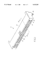
- a hard disk drive (HDD) connector 10 in accordance with the present invention comprises an insulative housing 12 defining a row of first passages 14 and a row of second passages 16 substantially parallel to each other.
- the passages 14, 16 extend between front and rear faces 18, 20 of the housing 12 for receiving and retaining first and second conductive contacts 22, 24 therein, respectively.
- the passages 14, 16 form conical openings 17 in the front face 18 for the insertion of corresponding pins of an HDD (not shown).
- the contacts 22, 24 comprise tail sections 26, 28 extending beyond the rear face 20 for being soldered to a circuit board (not shown).
- Board locks 30 are mounted on opposite ends of the housing 12 and extend beyond a bottom face 32 thereof for engaging with corresponding holes defined in the circuit board to retain the HDD connector 10 thereon.
- Positioning posts 34 are formed on the bottom face 32 of the housing 12 for properly positioning the HDD connector 10 on the circuit board.
- each passage 14, 16 is defined by opposite side walls 36, 38 each defining a notch 40, 42 in communication with the corresponding passage 14, 16.
- each first passage 14 corresponds to one second passage 16 and a partition 44 is formed therebetween.
- the notches 40, 42 of the first and second passages 14, 16 are arranged proximate the partition 44.
- Each first notch 40 forms a stop surface 46 in the first passage 14.
- each second notch 42 forms a stop surface (not shown) in the second passage 16.
- each contact 22, 24 comprises a U-shaped body 48, 50 having a central portion 52, 54 and two side portions 56, 58.
- the contacts 22, 24 are inserted into the corresponding passages 14, 16 with the side portions 56, 58 thereof abutting against the side walls 36, 38 of the corresponding passages 14, 16.
- Barbs 57, 59 are formed on edges of the side portions 56, 58 for interferentially engaging with inside faces of the corresponding passage 14, 16 thereby securing the contacts 22, 24 in the passages 14, 16.
- Each contact 22, 24 comprises a pair of resilient fingers 60, 62 extending from the side portions 56, 58 of the body 48, 50 toward the front face 18 of the housing 12 and converging toward each other for engagingly receiving the corresponding pin of the HDD therebetween.
- Each tail section 26, 28 extends from the central portion 52, 54 of the main body 48, 50 beyond the rear face 20 of the housing 12, in a direction opposite the fingers 60, 62.
- a retention section 64, 66 is formed between the central portion 52, 54 and the tail section 26, 28 and has opposite edges 68, 70 interferentially received in the notches 40, 42 of the corresponding passage 14, 16 for firmly retaining the contact 22, 24 therein.
- Each retention section 64, 66 forms shoulders 72, 74 for abutting against the stop surfaces 46 formed inside the corresponding passage 14, 16 (FIG. 5) for properly positioning the contact 22, 24 therein. It should be noted that the shoulders 72 are shown to be slightly distanced from the stop surfaces 46 for illustration purposes.
- a projection 90 (FIG. 3) is formed in each passage 14, 16 for separating the corresponding fingers 60, 62 from each other and pre-loading the fingers 60, 62 when the contact 22, 24 is inserted into the passage 14, 16.
- Two support arms 76, 78 extend from the side portions 56, 58 of the main body 48, 50 of each contact 22, 24 in a direction substantially opposite the fingers 60, 62.
- the support arms 76, 78 serving as extensions of the side portions 56, 58 of the main body 48, 50, firmly abut against the side walls 36, 38 of the corresponding passage 14, 16 for securely retaining the contact 22, 24 therein.
- each contact 22, 24 is bent 90 degrees for extending toward and being soldered to the circuit board to which the connector 10 is mounted. During the bending operation, a force is exerted on each contact 22, 24 causing undesired displacement thereof with respect to the housing 12. With the edges 68, 70 of the retention section 64, 66 of each contact 22, 24 retained in the corresponding notches 40, 42 of the housing 12, the retention section 64, 66 provides resistance against the bending force exerted on the contact 22, 24 thereby effectively eliminating or alleviating undesired displacement thereof
- each tail section 26, 28 comprises a soldering section 80, 82 substantially parallel to and aligned with the bottom face 32 of the housing 12 for being surface mounted to the circuit board.
- the soldering section 80, 82 may be substantially perpendicular to the bottom face 32 for being soldered to the circuit board by a through-hole technique.
- a spacer 84 is formed on the rear face 20 of the housing 12 and defines a plurality of spaced slots 86 for interferentially receiving the tail sections 26, 28 of the contacts 22, 24 thereby securely retaining the tail sections 26, 28 in position and effectively preventing the bent portion from springing back to its original position.
- the spacer 84 securely retains the tail sections 26, 28 thereby effectively maintaining the alignment of the soldering sections 80, 82.
Abstract
A hard disk drive connector includes an insulative housing defining passages for receiving and retaining contacts. Each passage is defined by opposite side walls. Opposite notches are defined in the side walls in communication with the passage. Each contact includes a U-shaped body received in the corresponding passage and a pair of pre-loaded, resilient fingers extending from the body for receiving therebetween and engaging with a corresponding pin of a hard disk drive. A retention section is formed on the body of each contact and has opposite edges interferentially received in the notches for firmly and stably retaining the contact in the passage. Each retention section forms shoulders for abutting against stop surfaces formed in the notches thereby properly positioning the contact in the passage. A tail section extends from the retention section and beyond the housing for being soldered to a circuit board. A spacer is formed on the housing and defines slots for interferentially receiving and retaining the tail sections therein. A pair of support arms extends from the body of each contact and tightly abuts against the side walls of the corresponding passage for stably supporting the contact in the passage. Barbs are formed on the body of the contact for interferentially engaging with walls of the corresponding passage thereby fixing the contact therein.
Description
1. Field of the Invention
The present invention generally relates to an electrical connector for connecting a hard disk drive (HDD) to a circuit board, and in particular to a contact of an HDD connector which is firmly secured in a housing of the connector.
2. The Prior Art
An HDD connector is mounted to a circuit board and is engageable with an HDD for establishing electrical connection between the HDD and the circuit board. A conventional housing of an HDD connector defines upper and lower rows of passages for receiving first and second contacts therein. Each contact has a tail section bent toward a circuit board for being soldered to the circuit board. A force is exerted on the contact during the bending operation whereby an undesired displacement of the contact with respect to the housing occurs and the securement of the contact in the housing becomes unstable.
In addition, in a surface-mounted HDD connector, a soldering portion of the tail of each contact is bent to be substantially parallel to a circuit board to which the connector is mounted. Due to mechanical properties of the contact, partial spring-back of the bent area of the contact occurs when the bending force is released, causing the soldering portion to be improperly aligned with the circuit board. Furthermore, warpage of the housing which frequently occurs in an injection-molded portion enhances the problem.
It is thus desirable to provide an HDD connector for addressing the problems discussed above.
Accordingly, an object of the present invention is to provide an HDD connector comprising contacts firmly secured in a housing thereof for resisting bending forces applied thereto.
Another object of the present invention is to provide an HDD connector comprising contacts stably fixed in a housing thereof.
A further object of the present invention is to provide an HDD connector comprising a spacer for securely retaining tails of contacts thereof in position and maintaining perfect alignment of the tails.
Still a further object of the present invention is to provide an HDD connector comprising stop means for properly positioning contacts thereof with respect to a housing.
To achieve the above objects, an HDD connector in accordance with the present invention comprises an insulative housing defining passages for receiving and retaining contacts. Each passage is defined by opposite side walls. Opposite notches are defined in the side walls in communication with the passage. Each contact includes a U-shaped body received in the corresponding passage and a pair of pre-loaded, resilient fingers extending from the body for receiving therebetween and engaging with a corresponding pin of a hard disk drive. A retention section is formed on the body of each contact and has opposite edges interferentially received in the notches for firmly and stably retaining the contact in the passage. Each retention section forms shoulders for abutting against stop surfaces formed in the notches thereby properly positioning the contact in the passage. A tail section extends from the retention section and beyond the housing for being soldered to a circuit board. A spacer is formed on the housing and defines slots for interferentially receiving and retaining the tail sections therein. A pair of support arms extends from the body of each contact and tightly abuts against the side walls of the corresponding passage for stably supporting the contact in the passage. Barbs are formed on the body of the contact for interferentially engaging with walls of the corresponding passage thereby fixing the contact therein.
The present invention will be apparent to those skilled in the art by reading the following description of a preferred embodiment thereof, with reference to the accompanying drawings, in which:
FIG. 1 is a perspective view of an electrical connector constructed in accordance with the present invention;
FIG. 2 is similar to FIG. 1 but taken from a different angle;
FIG. 3 is a cross-sectional view taken along line III--III of FIG. 1;
FIG. 4 is a cross-sectional view taken along line IV--IV of FIG. 3;
FIG. 5 is an enlarged view of encircled portion V of FIG. 4;
FIG. 6 is a perspective view of a first contact of the electrical connector of the present invention; and
FIG. 7 is a perspective view of a second contact of the electrical connector of the present invention.
Referring to the drawings and in particular to FIGS. 1-3, a hard disk drive (HDD) connector 10 in accordance with the present invention comprises an insulative housing 12 defining a row of first passages 14 and a row of second passages 16 substantially parallel to each other. The passages 14, 16 extend between front and rear faces 18, 20 of the housing 12 for receiving and retaining first and second conductive contacts 22, 24 therein, respectively. The passages 14, 16 form conical openings 17 in the front face 18 for the insertion of corresponding pins of an HDD (not shown). The contacts 22, 24 comprise tail sections 26, 28 extending beyond the rear face 20 for being soldered to a circuit board (not shown). Board locks 30 are mounted on opposite ends of the housing 12 and extend beyond a bottom face 32 thereof for engaging with corresponding holes defined in the circuit board to retain the HDD connector 10 thereon. Positioning posts 34 are formed on the bottom face 32 of the housing 12 for properly positioning the HDD connector 10 on the circuit board.
Also referring to FIGS. 4 and 5, each passage 14, 16 is defined by opposite side walls 36, 38 each defining a notch 40, 42 in communication with the corresponding passage 14, 16. In the embodiment illustrated, each first passage 14 corresponds to one second passage 16 and a partition 44 is formed therebetween. The notches 40, 42 of the first and second passages 14, 16 are arranged proximate the partition 44. Each first notch 40 forms a stop surface 46 in the first passage 14. Similarly, each second notch 42 forms a stop surface (not shown) in the second passage 16.
Also referring to FIGS. 6 and 7, each contact 22, 24 comprises a U-shaped body 48, 50 having a central portion 52, 54 and two side portions 56, 58. The contacts 22, 24 are inserted into the corresponding passages 14, 16 with the side portions 56, 58 thereof abutting against the side walls 36, 38 of the corresponding passages 14, 16. Barbs 57, 59 are formed on edges of the side portions 56, 58 for interferentially engaging with inside faces of the corresponding passage 14, 16 thereby securing the contacts 22, 24 in the passages 14, 16. Each contact 22, 24 comprises a pair of resilient fingers 60, 62 extending from the side portions 56, 58 of the body 48, 50 toward the front face 18 of the housing 12 and converging toward each other for engagingly receiving the corresponding pin of the HDD therebetween. Each tail section 26, 28 extends from the central portion 52, 54 of the main body 48, 50 beyond the rear face 20 of the housing 12, in a direction opposite the fingers 60, 62.
A retention section 64, 66 is formed between the central portion 52, 54 and the tail section 26, 28 and has opposite edges 68, 70 interferentially received in the notches 40, 42 of the corresponding passage 14, 16 for firmly retaining the contact 22, 24 therein. Each retention section 64, 66 forms shoulders 72, 74 for abutting against the stop surfaces 46 formed inside the corresponding passage 14, 16 (FIG. 5) for properly positioning the contact 22, 24 therein. It should be noted that the shoulders 72 are shown to be slightly distanced from the stop surfaces 46 for illustration purposes. A projection 90 (FIG. 3) is formed in each passage 14, 16 for separating the corresponding fingers 60, 62 from each other and pre-loading the fingers 60, 62 when the contact 22, 24 is inserted into the passage 14, 16.
Two support arms 76, 78 extend from the side portions 56, 58 of the main body 48, 50 of each contact 22, 24 in a direction substantially opposite the fingers 60, 62. The support arms 76, 78, serving as extensions of the side portions 56, 58 of the main body 48, 50, firmly abut against the side walls 36, 38 of the corresponding passage 14, 16 for securely retaining the contact 22, 24 therein.
The tail section 26, 28 of each contact 22, 24 is bent 90 degrees for extending toward and being soldered to the circuit board to which the connector 10 is mounted. During the bending operation, a force is exerted on each contact 22, 24 causing undesired displacement thereof with respect to the housing 12. With the edges 68, 70 of the retention section 64, 66 of each contact 22, 24 retained in the corresponding notches 40, 42 of the housing 12, the retention section 64, 66 provides resistance against the bending force exerted on the contact 22, 24 thereby effectively eliminating or alleviating undesired displacement thereof
In the embodiment illustrated, each tail section 26, 28 comprises a soldering section 80, 82 substantially parallel to and aligned with the bottom face 32 of the housing 12 for being surface mounted to the circuit board. However, the soldering section 80, 82 may be substantially perpendicular to the bottom face 32 for being soldered to the circuit board by a through-hole technique.
Referring to FIGS. 2 and 4, a spacer 84 is formed on the rear face 20 of the housing 12 and defines a plurality of spaced slots 86 for interferentially receiving the tail sections 26, 28 of the contacts 22, 24 thereby securely retaining the tail sections 26, 28 in position and effectively preventing the bent portion from springing back to its original position. For surface mounting the connector 10 to the circuit board, perfect alignment of the soldering sections 80, 82 is of vital importance. The spacer 84 securely retains the tail sections 26, 28 thereby effectively maintaining the alignment of the soldering sections 80, 82.
Although the present invention has been described with reference to the preferred embodiment, it is apparent to those skilled in the art that a variety of modifications and changes may be made without departing from the scope of the present invention which is intended to be defined by the appended claims.
Claims (1)
1. An electrical connector comprising:
an insulative housing defining passages between front and rear faces thereof, each passage being defined by opposite side walls of the housing and each side wall forming a notch in communication with the corresponding passage; and
conductive contacts received and retained in the passages, each contact comprising a U-shaped body having a central portion and opposite side portions, a pair of resilient fingers extending from the side portions toward the front face of the housing and converging toward each other, a retention section formed on the central portion, a tail extending from the retention section and beyond the rear face of the housing and adapted to be soldered to a circuit board, the retention section having opposite edges received and retained in the corresponding notches thereby firmly retaining the contact in the corresponding passage;
wherein the edges of the retention section of each contact are interferentially retained in the corresponding notches of the housing;
wherein each notch has a stop surface, and wherein the retention section of each contact has shoulders abutting against the stop surfaces of the corresponding notches for properly positioning the contact in the passage;
wherein two support arms extend from the side portions of the main body of each contact, the support arms tightly engaging with the side walls of the corresponding passage for stably supporting the contact in the corresponding passage;
wherein a spacer is formed on the rear face of the housing and defines a plurality of spaced slots for interferentially receiving and thus retaining the tails of the contacts therein;
wherein barbs are formed on the side portions of the main body of each contact for interferentially engaging with walls of the corresponding passage;
wherein a projection is formed in each passage for separating the fingers from each other thereby pre-loading the fingers;
further comprising board locks mounted to a bottom face of the housing;
further comprising positioning posts formed on a bottom face of the housing;
wherein the housing has two parallel rows of the passages;
wherein the two rows of passages are separated by a partition, and wherein the central portion of each contact is positioned to abut against the partition.
Priority Applications (3)
| Application Number | Priority Date | Filing Date | Title |
|---|---|---|---|
| US09/371,465 US6132263A (en) | 1999-08-10 | 1999-08-10 | Hard disk drive connector |
| TW088218481U TW430189U (en) | 1999-08-10 | 1999-10-29 | Hard disk drive connector |
| CN99240279.4U CN2405329Y (en) | 1999-08-10 | 1999-11-11 | Connector for hard disc driver |
Applications Claiming Priority (1)
| Application Number | Priority Date | Filing Date | Title |
|---|---|---|---|
| US09/371,465 US6132263A (en) | 1999-08-10 | 1999-08-10 | Hard disk drive connector |
Publications (1)
| Publication Number | Publication Date |
|---|---|
| US6132263A true US6132263A (en) | 2000-10-17 |
Family
ID=23464103
Family Applications (1)
| Application Number | Title | Priority Date | Filing Date |
|---|---|---|---|
| US09/371,465 Expired - Lifetime US6132263A (en) | 1999-08-10 | 1999-08-10 | Hard disk drive connector |
Country Status (3)
| Country | Link |
|---|---|
| US (1) | US6132263A (en) |
| CN (1) | CN2405329Y (en) |
| TW (1) | TW430189U (en) |
Cited By (1)
| Publication number | Priority date | Publication date | Assignee | Title |
|---|---|---|---|---|
| WO2019119758A1 (en) * | 2017-12-19 | 2019-06-27 | 华为技术有限公司 | A chip slot and network system |
Families Citing this family (1)
| Publication number | Priority date | Publication date | Assignee | Title |
|---|---|---|---|---|
| CN103367685B (en) * | 2012-04-17 | 2017-03-22 | 苏州方林科技股份有限公司 | Battery terminal and battery component with same |
Citations (8)
| Publication number | Priority date | Publication date | Assignee | Title |
|---|---|---|---|---|
| US4286837A (en) * | 1978-12-25 | 1981-09-01 | K.K. Elco International | Electrical connector, an insulator therefor and a fitting jig for an assembly of these |
| US4317609A (en) * | 1979-08-08 | 1982-03-02 | Gte Products Corporation | Electrical contact |
| US4717354A (en) * | 1984-11-19 | 1988-01-05 | Amp Incorporated | Solder cup connector |
| US5152700A (en) * | 1991-06-17 | 1992-10-06 | Litton Systems, Inc. | Printed circuit board connector system |
| US5286218A (en) * | 1991-12-27 | 1994-02-15 | Minnesota Mining And Manufacturing Company | Electric connector having means for fixing contacts |
| US5549480A (en) * | 1994-05-17 | 1996-08-27 | Tongrand Limited | Unitary connector allowing laterally variant positions of mating contacts of complementary connector |
| US5586915A (en) * | 1994-12-20 | 1996-12-24 | The Whitaker Corporation | Electrical connector with contacts at different insertion depths |
| US5641314A (en) * | 1995-06-30 | 1997-06-24 | The Whitaker Corporation | Memory card receptacle connector and contact terminal |
-
1999
- 1999-08-10 US US09/371,465 patent/US6132263A/en not_active Expired - Lifetime
- 1999-10-29 TW TW088218481U patent/TW430189U/en not_active IP Right Cessation
- 1999-11-11 CN CN99240279.4U patent/CN2405329Y/en not_active Expired - Lifetime
Patent Citations (8)
| Publication number | Priority date | Publication date | Assignee | Title |
|---|---|---|---|---|
| US4286837A (en) * | 1978-12-25 | 1981-09-01 | K.K. Elco International | Electrical connector, an insulator therefor and a fitting jig for an assembly of these |
| US4317609A (en) * | 1979-08-08 | 1982-03-02 | Gte Products Corporation | Electrical contact |
| US4717354A (en) * | 1984-11-19 | 1988-01-05 | Amp Incorporated | Solder cup connector |
| US5152700A (en) * | 1991-06-17 | 1992-10-06 | Litton Systems, Inc. | Printed circuit board connector system |
| US5286218A (en) * | 1991-12-27 | 1994-02-15 | Minnesota Mining And Manufacturing Company | Electric connector having means for fixing contacts |
| US5549480A (en) * | 1994-05-17 | 1996-08-27 | Tongrand Limited | Unitary connector allowing laterally variant positions of mating contacts of complementary connector |
| US5586915A (en) * | 1994-12-20 | 1996-12-24 | The Whitaker Corporation | Electrical connector with contacts at different insertion depths |
| US5641314A (en) * | 1995-06-30 | 1997-06-24 | The Whitaker Corporation | Memory card receptacle connector and contact terminal |
Cited By (4)
| Publication number | Priority date | Publication date | Assignee | Title |
|---|---|---|---|---|
| WO2019119758A1 (en) * | 2017-12-19 | 2019-06-27 | 华为技术有限公司 | A chip slot and network system |
| US11189970B2 (en) * | 2017-12-19 | 2021-11-30 | Huawei Technologies Co., Ltd. | Chip slot and network system |
| US20220085552A1 (en) * | 2017-12-19 | 2022-03-17 | Huawei Technologies Co., Ltd. | Memory slot and printed circuit board and network system |
| US11777257B2 (en) * | 2017-12-19 | 2023-10-03 | Huawei Technologies Co., Ltd. | Memory slot and printed circuit board and network system |
Also Published As
| Publication number | Publication date |
|---|---|
| TW430189U (en) | 2001-04-11 |
| CN2405329Y (en) | 2000-11-08 |
Similar Documents
| Publication | Publication Date | Title |
|---|---|---|
| US4781612A (en) | Socket for single in-line memory module | |
| JP3018007B2 (en) | socket | |
| US7175447B2 (en) | Backplane connector | |
| US5004434A (en) | Printed circuit board edge connector | |
| JP2835563B2 (en) | Edge connectors for printed circuit boards | |
| US5676555A (en) | Card edge connector having means for applying inward transverse force on printed wiring boards | |
| US7402080B2 (en) | Electrical connector for reliably mounted on a printed circuit board | |
| US4973270A (en) | Circuit panel socket with cloverleaf contact | |
| US7497700B2 (en) | Electrical connector | |
| US6244875B1 (en) | Electrical connector | |
| JP2005525684A (en) | Edge card connector assembly with terminals with adjusted impedance | |
| US6634911B1 (en) | Contact for electrical connector | |
| KR0138832B1 (en) | Edge mounted circuit board electrical connector | |
| US7112072B2 (en) | Ground bus for an electrical connector | |
| US5575663A (en) | Electrical connector for mounting to an edge of a circuit board | |
| US20050026474A1 (en) | Electrical connector having improved terminals | |
| US6736650B1 (en) | Electrical connector with terminal retention mechanism | |
| US6077092A (en) | Electrical connector having stabilizing structure for spacer and terminal | |
| US6450826B1 (en) | Contact of electrical connector | |
| JP4102747B2 (en) | connector | |
| JPH07211370A (en) | Electric connector to be mounted on printed circuit board | |
| US6106308A (en) | Contact of an electrical connector having solder terminal capable of fitting with a housing of the connector | |
| US6371772B1 (en) | Electrical connector with enhanced contacts | |
| US6371802B1 (en) | Header connector with stabilizer | |
| EP0400378A2 (en) | Circuit panel socket with cloverleaf contact |
Legal Events
| Date | Code | Title | Description |
|---|---|---|---|
| AS | Assignment |
Owner name: HON HAI PRECISION IND. CO., LTD., TAIWAN Free format text: ASSIGNMENT OF ASSIGNORS INTEREST;ASSIGNOR:WU, JERRY;REEL/FRAME:010163/0398 Effective date: 19990728 |
|
| STCF | Information on status: patent grant |
Free format text: PATENTED CASE |
|
| FPAY | Fee payment |
Year of fee payment: 4 |
|
| FPAY | Fee payment |
Year of fee payment: 8 |
|
| FPAY | Fee payment |
Year of fee payment: 12 |