US6137727A - Reduction of oxide stress through the use of forward biased body voltage - Google Patents
Reduction of oxide stress through the use of forward biased body voltage Download PDFInfo
- Publication number
- US6137727A US6137727A US09/490,353 US49035300A US6137727A US 6137727 A US6137727 A US 6137727A US 49035300 A US49035300 A US 49035300A US 6137727 A US6137727 A US 6137727A
- Authority
- US
- United States
- Prior art keywords
- cell
- read
- volts
- voltage
- positive voltage
- Prior art date
- Legal status (The legal status is an assumption and is not a legal conclusion. Google has not performed a legal analysis and makes no representation as to the accuracy of the status listed.)
- Expired - Lifetime
Links
- 238000000034 method Methods 0.000 claims abstract description 15
- 239000000758 substrate Substances 0.000 claims description 3
- 230000005669 field effect Effects 0.000 claims description 2
- 230000007423 decrease Effects 0.000 description 5
- 238000012986 modification Methods 0.000 description 4
- 230000004048 modification Effects 0.000 description 4
- 238000010586 diagram Methods 0.000 description 3
- 238000004377 microelectronic Methods 0.000 description 2
- 239000004065 semiconductor Substances 0.000 description 2
- 230000005689 Fowler Nordheim tunneling Effects 0.000 description 1
- 239000002784 hot electron Substances 0.000 description 1
- 239000011159 matrix material Substances 0.000 description 1
Images

Classifications
-
- G—PHYSICS
- G11—INFORMATION STORAGE
- G11C—STATIC STORES
- G11C16/00—Erasable programmable read-only memories
- G11C16/02—Erasable programmable read-only memories electrically programmable
- G11C16/06—Auxiliary circuits, e.g. for writing into memory
- G11C16/26—Sensing or reading circuits; Data output circuits
-
- G—PHYSICS
- G11—INFORMATION STORAGE
- G11C—STATIC STORES
- G11C16/00—Erasable programmable read-only memories
- G11C16/02—Erasable programmable read-only memories electrically programmable
- G11C16/04—Erasable programmable read-only memories electrically programmable using variable threshold transistors, e.g. FAMOS
- G11C16/0408—Erasable programmable read-only memories electrically programmable using variable threshold transistors, e.g. FAMOS comprising cells containing floating gate transistors
- G11C16/0416—Erasable programmable read-only memories electrically programmable using variable threshold transistors, e.g. FAMOS comprising cells containing floating gate transistors comprising cells containing a single floating gate transistor and no select transistor, e.g. UV EPROM
Definitions
- This invention relates generally to the art of microelectronic integrated circuits. More specifically, this invention relates to flash Electrically Erasable Programmable Read Only Memory (EEPROM) devices. Even more specifically, this invention relates to a method to read flash Electrically Erasable Programmable Read Only Memory (EEPROM) devices to reduce oxide stress.
- EEPROM Electrically Erasable Programmable Read Only Memory
- a microelectronic Electrically Erasable Programmable Read-Only Memory (Flash EEPROM) device includes an array of cells that can be independently programmed and read. The size of each cell and thereby the memory device are made small by omitting select transistors that would enable the cells to be erased independently. As a result, all of the cells must be erased simultaneously as a block.
- a memory of this type includes individual Metal-Oxide-Semiconductor (MOS) field effect transistor memory cells, each of which includes a source, drain, floating gate and control gate to which various voltages are applied to program the cell with a binary "1" or "0” or to erase all of the cells as a block.
- MOS Metal-Oxide-Semiconductor
- the cells are connected in a rectangular array of rows and columns, with the control gates of the cells in a row being connected to a respective wordline and the drains of the cells in a column being connected to a respective bitline.
- the sources of the cells are connected together to a common source. This arrangement is known as a NOR memory configuration.
- a cell is programmed by applying typically 8-9 volts to the control gate, approximately 5 volts to the drain and grounding the source, which causes hot electrons to be injected from the drain depletion region into the floating gate. Upon removal of the programming voltages, the injected electrons are trapped in the floating gate and create a negative charge therein that increases the threshold voltage of the cell to a value in excess of approximately 4 volts.
- a cell can be erased in several ways. In one arrangement, applying typically 12 volts to the source, grounding the control gate and allowing the drain to float erases a cell. This causes the electrons that were injected into the floating gate during programming to be removed by Fowler-Nordheim tunneling from the floating gate through the thin tunnel oxide layer to the source. Alternatively, applying a negative voltage on the order of minus 10 volts to the control gate, applying 5 volts to the source and allowing the drain to float can erase a cell.
- the cell is read by applying typically 5 volts to the control gate, 1-2 volts to the bitline to which the drain is connected, grounding the source, and sensing the bitline current. If the cell is programmed and the threshold voltage is relatively high ( ⁇ 4 volts), the bitline current will be zero or at least relatively low. If the cell is not programmed or erased, the threshold voltage will be relatively low ( ⁇ 2 volts), the control gate voltage will enhance the channel, and the bitline current will be relatively high.
- Oxide stress can cause electrons to tunnel across the tunnel oxide to the floating gate. This causes the threshold voltage, V t , to increase and is referred to as charge gain.
- the cause of the oxide stress is the control gate voltage that is applied causes current to flow in the cell and is given approximately by the equation
- V GS is the voltage from the gate to the source
- k is a proportional constant
- V t is the threshold voltage of the cell. It can be seen from the equation that increasing V GS increases I. Unfortunately, increasing V GS also increases the oxide stress as can be seen from the equation for the oxide voltage V FG .
- the voltage V FG is proportional to the control gate voltage V CG as follows:
- V GS would need to be some minimum value.
- Another alternative to maintain the current and reducing V GS would be to decrease V t .
- the direct way to do this would be to increase the positive charge on the floating gate. In that case V FG would increase and the oxide stress would increase so this alternative would not be a good approach.
- EEPROM Electrically-Erasable Programmable Read Only Memory
- a positive voltage is applied to the bitline to which the cell being read is attached, a positive voltage is applied to the wordline to which the cell being read is attached and a positive voltage is applied to the p-well to which the cell being read is attached.
- the positive voltage applied to the bitline to which the cell being read is attached is between 1 and 2 volts.
- the positive voltage applied to the wordline to which the cell being read is attached is between 5 and 8 volts and the positive voltage applied to the p-well is approximately 0.4 volts.
- zero volts is applied to the bitlines to which the cell being read is not attached and to wordlines to which the cell being read is not attached.
- zero volts is applied to the common source terminal.
- the described method thus provides a method of reading a flash memory cell that reduces the oxide stress during read operation.
- FIG. 1A is a simplified electrical schematic diagram of a flash EEPROM device showing an array of memory cells and control elements
- FIG. 1B shows a single flash memory cell with read voltages applied to the terminals of the flash memory cell in accordance with the prior art
- FIG. 2A shows a single flash memory cell with read voltages applied to the terminals of the flash memory cell in accordance with the present invention
- FIG. 2B illustrates the control gate voltage and the floating gate voltage in relation to the capacitance of the gate oxide and capacitance of the tunnel oxide
- FIG. 3A shows a single flash memory cell illustrating the connections to the terminals of the flash memory cell
- FIG. 3B is a simplified electrical schematic diagram of several flash EEPROM cells showing voltages applied to the terminals of the several flash memory cells during read.
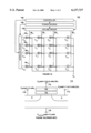
- FIG. 1A illustrates the basic configuration of a NOR type flash Electrically Erasable Programmable Read-Only Memory (EEPROM) device 100 to which the present invention is advantageously applied.
- the memory device 100 is a plurality of core or memory cells that are arranged in a rectangular matrix or array of rows and columns. Each row is associated with a wordline, whereas each column is associated with a bitline.
- the sources of all of the memory cells are connected to a common terminal, V S .
- bitlines are designated BL 0 to BL n and the wordlines are designated as WL 0 to WL m .
- a bitline driver 102 applies appropriate voltages to the bitlines, whereas a wordline driver 104 applies appropriate voltages to the wordlines.
- the voltages applied to the drivers 102 and 104 are generated by a power source or supply 106 under the control of a controller 108 that is typically on-chip logic circuitry.
- the controller 108 also controls the drivers 102 and 104 to address the memory cells individually or collectively as will be described below.
- a memory cell is located at each junction of a wordline and a bitline.
- Each cell includes a Metal-Oxide-Semiconductor (MOS) Field-Effect-Transistor (FET) having a source, drain, gate oxide and control gate.
- MOS Metal-Oxide-Semiconductor
- FET Field-Effect-Transistor
- the cells of a flash EEPROM differ from conventional FETs in that they additionally include a floating gate and tunnel oxide layer disposed underneath the control gate.
- the cells illustrated in FIG. 1A are designated using the notation T n ,m, where m is the row (wordline) number and n is the column (bitline) number.
- the control gates of the cells are connected to respective wordlines, and the drains of the cells are connected to respective bitlines as illustrated.
- the sources of all of the cells are connected to the common terminal V S , which is connected to the power supply 106. The connection to the power supply 106 is not shown.
- FIG. 1B shows a single flash memory cell 110 with read voltages applied to the terminals of the flash memory cell 110 during a read operation in accordance with the prior art.
- a read voltage typically of from 5 to 8 volts is applied to the terminal 112 via the wordline attached to the gate of the cell being read.
- a read voltage of 1 to 2 volts is applied to the terminal 114 via the bitline attached to the drain of the cell being read.
- Zero voltage is applied to the source terminal 116 via a line that is attached to a common terminal. As is known in the flash memory art, all of the sources are connected to a common terminal. Zero voltage is applied to the terminal 118 that is connected to the substrate, which is also common to all the cells in the device.
- a voltage differential of from 5-8 volts is applied between the gate terminal and source terminal of all of the bits attached to the wordline of the cell being read.
- the relatively high gate-to-source voltage can cause stress in the tunnel oxide that results in electrons being leaked to the floating gate causing a charge gain.
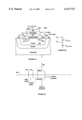
- FIG. 2A shows a single flash memory cell 200 with read voltages applied to the terminals of the flash memory cell 200 in accordance with the present invention.
- a voltage of typically 5 to 8 volts is applied to the control gate 202 via terminal 204.
- the source is grounded (0 volts) as indicated at 206, a voltage of 1 to 2 volts is applied to the drain 208 via terminal 210 and a voltage of approximately 0.4 volts is applied to the P-well 212 via terminal 214.
- V SB is voltage difference between the source and body (p-well). Therefore, if V source is zero and V body is 0.4 volts, the threshold voltage V t decreases. Therefore, V CG decreases, which decreases V FG and the oxide stress, but since V t also decreases the minimum required current level necessary to read the cell will be maintained.
- FIG. 2B illustrates the control gate voltage V CG and the floating gate voltage V FG in relation of the capacitance of the gate oxide C CGoxide and capacitance of the tunnel oxide C tunnel oxide.
- V FG ⁇ V CG (C gate oxide)/(C gate oxide +C tunnel oxide).
- FIG. 3A is a single flash memory cell 300 illustrating the connections to the terminals of the flash memory cell 300.
- FIG. 3B is a simplified electrical schematic diagram of several flash EEPROM cells as shown in FIG. 3A showing the voltages applied to the terminals of the flash memory cells during the reading of one of the flash memory cells. Shown in FIG. 3B are two wordlines WL 1 and WL m and two bitlines BL 1 and BL n . At the intersection of each wordline and each bitline is located a memory cell, such as memory cell 300. Wordline WL 1 is connected to the control gate of memory cell 300 and the control gate of memory cell 304 and to the control gates of all memory cells in between. Similarly, wordline WL m is connected to the control gate of memory cell 302 and to the control gate of memory cell 306 and to the control gates of all memory cells in between.
- Bitline BL 1 is connected to the drains of memory cell 300 and memory cell 302 and the drains of all memory cells in between.
- bitline BL n is connected to the drains of memory cell 304 and memory cell 306 and the drains of all memory cells in between.
- Lines 308 electrically connect the sources of all memory cells to a common terminal 310.
- Lines 312 electrically connect the P-wells of all the memory cells to a common terminal 314.
- a voltage of between 5 and 8 volts is applied to WL 1 , a voltage of 0 volts is applied to the remaining bitlines including WL m .
- a voltage of 1 to 2 volts is applied to BL 1 and a voltage of 0 volts is applied to the remaining bitlines including BL n .
- the common source terminal 310 is connected to ground (0 volts) and a positive voltage of approximately 0.4 volts is applied to the common P-well terminal 314.
- the present invention overcomes the limitations of the prior art and fulfills the need for a method of reading a flash memory cell that reduces the oxide stress during the read operation.
Abstract
Description
I=k(V.sub.GS -V.sub.t).sup.n,
V.sub.FG ˜V.sub.CG (C.sub.gate oxide)/(C.sub.gate oxide +C.sub.tunnel oxide)
I=k(V.sub.GS -V.sub.t).sup.n,
Claims (7)
Priority Applications (1)
| Application Number | Priority Date | Filing Date | Title |
|---|---|---|---|
| US09/490,353 US6137727A (en) | 2000-01-24 | 2000-01-24 | Reduction of oxide stress through the use of forward biased body voltage |
Applications Claiming Priority (1)
| Application Number | Priority Date | Filing Date | Title |
|---|---|---|---|
| US09/490,353 US6137727A (en) | 2000-01-24 | 2000-01-24 | Reduction of oxide stress through the use of forward biased body voltage |
Publications (1)
| Publication Number | Publication Date |
|---|---|
| US6137727A true US6137727A (en) | 2000-10-24 |
Family
ID=23947684
Family Applications (1)
| Application Number | Title | Priority Date | Filing Date |
|---|---|---|---|
| US09/490,353 Expired - Lifetime US6137727A (en) | 2000-01-24 | 2000-01-24 | Reduction of oxide stress through the use of forward biased body voltage |
Country Status (1)
| Country | Link |
|---|---|
| US (1) | US6137727A (en) |
Cited By (6)
| Publication number | Priority date | Publication date | Assignee | Title |
|---|---|---|---|---|
| US6272047B1 (en) * | 1999-12-17 | 2001-08-07 | Micron Technology, Inc. | Flash memory cell |
| US6363016B1 (en) * | 2000-10-12 | 2002-03-26 | Xilinx, Inc. | Method for enhancement of non-volatile memory cell read current |
| US6502113B1 (en) * | 1998-11-23 | 2002-12-31 | John E. Crawford | Negotiation manager incorporating clause modification and markers for tracking negotiation progress |
| US6549465B2 (en) * | 2001-02-28 | 2003-04-15 | Sharp Kabushiki Kaisha | Nonvolatile semiconductor memory well voltage setting circuit without latchup and semiconductor memory device provided with the circuit |
| US20040196714A1 (en) * | 2002-04-09 | 2004-10-07 | Powerchip Seimiconductor Corporation | Structure, fabrication method and operating method for flash memory |
| US20080123435A1 (en) * | 2006-07-10 | 2008-05-29 | Macronix International Co., Ltd. | Operation of Nonvolatile Memory Having Modified Channel Region Interface |
Citations (7)
| Publication number | Priority date | Publication date | Assignee | Title |
|---|---|---|---|---|
| US5042009A (en) * | 1988-12-09 | 1991-08-20 | Waferscale Integration, Inc. | Method for programming a floating gate memory device |
| US5341342A (en) * | 1992-12-18 | 1994-08-23 | National Semiconductor Corporation | Flash memory cell structure |
| US5412603A (en) * | 1994-05-06 | 1995-05-02 | Texas Instruments Incorporated | Method and circuitry for programming floating-gate memory cell using a single low-voltage supply |
| US5511022A (en) * | 1988-12-15 | 1996-04-23 | Samsung Electronics Co., Ltd. | Depletion mode NAND string electrically erasable programmable semiconductor memory device and method for erasing and programming thereof |
| US5646886A (en) * | 1995-05-24 | 1997-07-08 | National Semiconductor Corporation | Flash memory having segmented array for improved operation |
| US5770963A (en) * | 1991-12-09 | 1998-06-23 | Fujitsu Limited | Flash memory with improved erasability and its circuitry |
| US5991203A (en) * | 1997-12-06 | 1999-11-23 | Samsung Electronics Co., Ltd. | Circuit and method of erasing a nonvolatile semiconductor memory |
-
2000
- 2000-01-24 US US09/490,353 patent/US6137727A/en not_active Expired - Lifetime
Patent Citations (7)
| Publication number | Priority date | Publication date | Assignee | Title |
|---|---|---|---|---|
| US5042009A (en) * | 1988-12-09 | 1991-08-20 | Waferscale Integration, Inc. | Method for programming a floating gate memory device |
| US5511022A (en) * | 1988-12-15 | 1996-04-23 | Samsung Electronics Co., Ltd. | Depletion mode NAND string electrically erasable programmable semiconductor memory device and method for erasing and programming thereof |
| US5770963A (en) * | 1991-12-09 | 1998-06-23 | Fujitsu Limited | Flash memory with improved erasability and its circuitry |
| US5341342A (en) * | 1992-12-18 | 1994-08-23 | National Semiconductor Corporation | Flash memory cell structure |
| US5412603A (en) * | 1994-05-06 | 1995-05-02 | Texas Instruments Incorporated | Method and circuitry for programming floating-gate memory cell using a single low-voltage supply |
| US5646886A (en) * | 1995-05-24 | 1997-07-08 | National Semiconductor Corporation | Flash memory having segmented array for improved operation |
| US5991203A (en) * | 1997-12-06 | 1999-11-23 | Samsung Electronics Co., Ltd. | Circuit and method of erasing a nonvolatile semiconductor memory |
Cited By (14)
| Publication number | Priority date | Publication date | Assignee | Title |
|---|---|---|---|---|
| US6502113B1 (en) * | 1998-11-23 | 2002-12-31 | John E. Crawford | Negotiation manager incorporating clause modification and markers for tracking negotiation progress |
| US6449189B2 (en) | 1999-12-17 | 2002-09-10 | Micron Technology, Inc. | Flash memory cell for high efficiency programming |
| US6384447B2 (en) | 1999-12-17 | 2002-05-07 | Micron Technology, Inc. | Flash memory cell for high efficiency programming |
| US6434045B2 (en) | 1999-12-17 | 2002-08-13 | Micron Technology, Inc. | Flash memory cell for high efficiency programming |
| US6445620B2 (en) | 1999-12-17 | 2002-09-03 | Micron Technology, Inc. | Flash memory cell for high efficiency programming |
| US6445619B1 (en) | 1999-12-17 | 2002-09-03 | Micron Technology, Inc. | Flash memory cell for high efficiency programming |
| US6272047B1 (en) * | 1999-12-17 | 2001-08-07 | Micron Technology, Inc. | Flash memory cell |
| US6577537B2 (en) | 1999-12-17 | 2003-06-10 | Micron Technology, Inc. | Flash memory cell for high efficiency programming |
| US6587376B2 (en) | 1999-12-17 | 2003-07-01 | Micron Technology, Inc. | Flash memory cell for high efficiency programming |
| US6363016B1 (en) * | 2000-10-12 | 2002-03-26 | Xilinx, Inc. | Method for enhancement of non-volatile memory cell read current |
| US6549465B2 (en) * | 2001-02-28 | 2003-04-15 | Sharp Kabushiki Kaisha | Nonvolatile semiconductor memory well voltage setting circuit without latchup and semiconductor memory device provided with the circuit |
| US20040196714A1 (en) * | 2002-04-09 | 2004-10-07 | Powerchip Seimiconductor Corporation | Structure, fabrication method and operating method for flash memory |
| US6834011B2 (en) * | 2002-04-09 | 2004-12-21 | Powerchip Semiconductor Corporation | Structure, fabrication method and operating method for flash memory |
| US20080123435A1 (en) * | 2006-07-10 | 2008-05-29 | Macronix International Co., Ltd. | Operation of Nonvolatile Memory Having Modified Channel Region Interface |
Similar Documents
| Publication | Publication Date | Title |
|---|---|---|
| US5511022A (en) | Depletion mode NAND string electrically erasable programmable semiconductor memory device and method for erasing and programming thereof | |
| US6459623B1 (en) | EEPROM erasing method | |
| US5457652A (en) | Low voltage EEPROM | |
| US6240016B1 (en) | Method to reduce read gate disturb for flash EEPROM application | |
| US6853598B2 (en) | Non-volatile memory with test rows for disturb detection | |
| JP3653186B2 (en) | Nonvolatile memory device programming method | |
| US5491657A (en) | Method for bulk (or byte) charging and discharging an array of flash EEPROM memory cells | |
| US5357465A (en) | Single transistor EEPROM memory cell | |
| US5790456A (en) | Multiple bits-per-cell flash EEPROM memory cells with wide program and erase Vt window | |
| JPH1093058A (en) | Flash memory device | |
| US5521867A (en) | Adjustable threshold voltage conversion circuit | |
| JP3895816B2 (en) | Nonvolatile semiconductor storage device and control method thereof, memory card, and storage system | |
| US5875130A (en) | Method for programming flash electrically erasable programmable read-only memory | |
| KR100379553B1 (en) | A array of flash memory cell and method for programming of data thereby and method for erased of data thereby | |
| US6285588B1 (en) | Erase scheme to tighten the threshold voltage distribution of EEPROM flash memory cells | |
| US6141255A (en) | 1 transistor cell for EEPROM application | |
| US6510085B1 (en) | Method of channel hot electron programming for short channel NOR flash arrays | |
| US6233175B1 (en) | Self-limiting multi-level programming states | |
| US6137727A (en) | Reduction of oxide stress through the use of forward biased body voltage | |
| JP3342878B2 (en) | Nonvolatile semiconductor memory device | |
| US6272046B1 (en) | Individual source line to decrease column leakage | |
| US6208561B1 (en) | Method to reduce capacitive loading in flash memory X-decoder for accurate voltage control at wordlines and select lines | |
| US6160740A (en) | Method to provide a reduced constant E-field during erase of EEPROMs for reliability improvement | |
| KR20010013737A (en) | Control circuit for a non-volatile semi-conductor memory system | |
| KR20010072189A (en) | Semiconductor device with a non-volatile memory |
Legal Events
| Date | Code | Title | Description |
|---|---|---|---|
| AS | Assignment |
Owner name: ADVANCED MICRO DEVICES, INC., CALIFORNIA Free format text: ASSIGNMENT OF ASSIGNORS INTEREST;ASSIGNOR:CLEVELAND, LEE EDWARD;REEL/FRAME:010545/0300 Effective date: 20000119 |
|
| STCF | Information on status: patent grant |
Free format text: PATENTED CASE |
|
| FPAY | Fee payment |
Year of fee payment: 4 |
|
| AS | Assignment |
Owner name: SPANSION INC., CALIFORNIA Free format text: ASSIGNMENT OF ASSIGNORS INTEREST;ASSIGNOR:ADVANCED MICRO DEVICES, INC.;REEL/FRAME:019028/0656 Effective date: 20070131 |
|
| AS | Assignment |
Owner name: SPANSION LLC, CALIFORNIA Free format text: ASSIGNMENT OF ASSIGNORS INTEREST;ASSIGNOR:SPANSION INC.;REEL/FRAME:019069/0094 Effective date: 20070131 |
|
| FPAY | Fee payment |
Year of fee payment: 8 |
|
| AS | Assignment |
Owner name: BARCLAYS BANK PLC,NEW YORK Free format text: SECURITY AGREEMENT;ASSIGNORS:SPANSION LLC;SPANSION INC.;SPANSION TECHNOLOGY INC.;AND OTHERS;REEL/FRAME:024522/0338 Effective date: 20100510 Owner name: BARCLAYS BANK PLC, NEW YORK Free format text: SECURITY AGREEMENT;ASSIGNORS:SPANSION LLC;SPANSION INC.;SPANSION TECHNOLOGY INC.;AND OTHERS;REEL/FRAME:024522/0338 Effective date: 20100510 |
|
| FPAY | Fee payment |
Year of fee payment: 12 |
|
| AS | Assignment |
Owner name: SPANSION INC., CALIFORNIA Free format text: RELEASE BY SECURED PARTY;ASSIGNOR:BARCLAYS BANK PLC;REEL/FRAME:035201/0159 Effective date: 20150312 Owner name: SPANSION LLC, CALIFORNIA Free format text: RELEASE BY SECURED PARTY;ASSIGNOR:BARCLAYS BANK PLC;REEL/FRAME:035201/0159 Effective date: 20150312 Owner name: SPANSION TECHNOLOGY LLC, CALIFORNIA Free format text: RELEASE BY SECURED PARTY;ASSIGNOR:BARCLAYS BANK PLC;REEL/FRAME:035201/0159 Effective date: 20150312 |
|
| AS | Assignment |
Owner name: MORGAN STANLEY SENIOR FUNDING, INC., NEW YORK Free format text: SECURITY INTEREST;ASSIGNORS:CYPRESS SEMICONDUCTOR CORPORATION;SPANSION LLC;REEL/FRAME:035240/0429 Effective date: 20150312 |
|
| AS | Assignment |
Owner name: CYPRESS SEMICONDUCTOR CORPORATION, CALIFORNIA Free format text: ASSIGNMENT OF ASSIGNORS INTEREST;ASSIGNOR:SPANSION, LLC;REEL/FRAME:036017/0625 Effective date: 20150601 |
|
| AS | Assignment |
Owner name: CYPRESS SEMICONDUCTOR CORPORATION, CALIFORNIA Free format text: PARTIAL RELEASE OF SECURITY INTEREST IN PATENTS;ASSIGNOR:MORGAN STANLEY SENIOR FUNDING, INC., AS COLLATERAL AGENT;REEL/FRAME:039708/0001 Effective date: 20160811 Owner name: SPANSION LLC, CALIFORNIA Free format text: PARTIAL RELEASE OF SECURITY INTEREST IN PATENTS;ASSIGNOR:MORGAN STANLEY SENIOR FUNDING, INC., AS COLLATERAL AGENT;REEL/FRAME:039708/0001 Effective date: 20160811 |
|
| AS | Assignment |
Owner name: MONTEREY RESEARCH, LLC, CALIFORNIA Free format text: ASSIGNMENT OF ASSIGNORS INTEREST;ASSIGNOR:CYPRESS SEMICONDUCTOR CORPORATION;REEL/FRAME:040911/0238 Effective date: 20160811 |
|
| AS | Assignment |
Owner name: MORGAN STANLEY SENIOR FUNDING, INC., NEW YORK Free format text: CORRECTIVE ASSIGNMENT TO CORRECT THE 8647899 PREVIOUSLY RECORDED ON REEL 035240 FRAME 0429. ASSIGNOR(S) HEREBY CONFIRMS THE SECURITY INTERST;ASSIGNORS:CYPRESS SEMICONDUCTOR CORPORATION;SPANSION LLC;REEL/FRAME:058002/0470 Effective date: 20150312 |