US6140153A - Lead frame, the manufacturing method, semiconductor device and the manufacturing method - Google Patents

Lead frame, the manufacturing method, semiconductor device and the manufacturing method Download PDF

Info

Publication number
US6140153A
US6140153A US09/084,189 US8418998A US6140153A US 6140153 A US6140153 A US 6140153A US 8418998 A US8418998 A US 8418998A US 6140153 A US6140153 A US 6140153A
Authority
US
United States
Prior art keywords
layer
lead frame
etching stop
stop layer
etching
Prior art date
Legal status (The legal status is an assumption and is not a legal conclusion. Google has not performed a legal analysis and makes no representation as to the accuracy of the status listed.)
Expired - Fee Related
Application number
US09/084,189
Inventor
Kenji Ohsawa
Hidetoshi Kusano
Current Assignee (The listed assignees may be inaccurate. Google has not performed a legal analysis and makes no representation or warranty as to the accuracy of the list.)
Sony Corp
Original Assignee
Sony Corp
Priority date (The priority date is an assumption and is not a legal conclusion. Google has not performed a legal analysis and makes no representation as to the accuracy of the date listed.)
Filing date
Publication date
Application filed by Sony Corp filed Critical Sony Corp
Assigned to SONY CORPORATION reassignment SONY CORPORATION ASSIGNMENT OF ASSIGNORS INTEREST (SEE DOCUMENT FOR DETAILS). Assignors: KUSANO, HIDETOSHI, OHSAWA, KENJI
Application granted granted Critical
Priority to US09/702,456 priority Critical patent/US6403402B1/en
Priority to US09/702,437 priority patent/US6369441B1/en
Priority to US09/702,457 priority patent/US6351025B1/en
Publication of US6140153A publication Critical patent/US6140153A/en
Anticipated expiration legal-status Critical
Expired - Fee Related legal-status Critical Current

Links

Images

Classifications

    • HELECTRICITY
    • H01ELECTRIC ELEMENTS
    • H01LSEMICONDUCTOR DEVICES NOT COVERED BY CLASS H10
    • H01L23/00Details of semiconductor or other solid state devices
    • H01L23/48Arrangements for conducting electric current to or from the solid state body in operation, e.g. leads, terminal arrangements ; Selection of materials therefor
    • H01L23/488Arrangements for conducting electric current to or from the solid state body in operation, e.g. leads, terminal arrangements ; Selection of materials therefor consisting of soldered or bonded constructions
    • H01L23/495Lead-frames or other flat leads
    • H01L23/49579Lead-frames or other flat leads characterised by the materials of the lead frames or layers thereon
    • H01L23/49582Metallic layers on lead frames
    • HELECTRICITY
    • H01ELECTRIC ELEMENTS
    • H01LSEMICONDUCTOR DEVICES NOT COVERED BY CLASS H10
    • H01L23/00Details of semiconductor or other solid state devices
    • H01L23/48Arrangements for conducting electric current to or from the solid state body in operation, e.g. leads, terminal arrangements ; Selection of materials therefor
    • H01L23/50Arrangements for conducting electric current to or from the solid state body in operation, e.g. leads, terminal arrangements ; Selection of materials therefor for integrated circuit devices, e.g. power bus, number of leads
    • HELECTRICITY
    • H01ELECTRIC ELEMENTS
    • H01LSEMICONDUCTOR DEVICES NOT COVERED BY CLASS H10
    • H01L21/00Processes or apparatus adapted for the manufacture or treatment of semiconductor or solid state devices or of parts thereof
    • H01L21/02Manufacture or treatment of semiconductor devices or of parts thereof
    • H01L21/04Manufacture or treatment of semiconductor devices or of parts thereof the devices having at least one potential-jump barrier or surface barrier, e.g. PN junction, depletion layer or carrier concentration layer
    • H01L21/48Manufacture or treatment of parts, e.g. containers, prior to assembly of the devices, using processes not provided for in a single one of the subgroups H01L21/06 - H01L21/326
    • H01L21/4814Conductive parts
    • H01L21/4821Flat leads, e.g. lead frames with or without insulating supports
    • H01L21/4828Etching
    • HELECTRICITY
    • H01ELECTRIC ELEMENTS
    • H01LSEMICONDUCTOR DEVICES NOT COVERED BY CLASS H10
    • H01L23/00Details of semiconductor or other solid state devices
    • H01L23/16Fillings or auxiliary members in containers or encapsulations, e.g. centering rings
    • H01L23/18Fillings characterised by the material, its physical or chemical properties, or its arrangement within the complete device
    • H01L23/24Fillings characterised by the material, its physical or chemical properties, or its arrangement within the complete device solid or gel at the normal operating temperature of the device
    • HELECTRICITY
    • H01ELECTRIC ELEMENTS
    • H01LSEMICONDUCTOR DEVICES NOT COVERED BY CLASS H10
    • H01L23/00Details of semiconductor or other solid state devices
    • H01L23/28Encapsulations, e.g. encapsulating layers, coatings, e.g. for protection
    • H01L23/31Encapsulations, e.g. encapsulating layers, coatings, e.g. for protection characterised by the arrangement or shape
    • H01L23/3107Encapsulations, e.g. encapsulating layers, coatings, e.g. for protection characterised by the arrangement or shape the device being completely enclosed
    • H01L23/3121Encapsulations, e.g. encapsulating layers, coatings, e.g. for protection characterised by the arrangement or shape the device being completely enclosed a substrate forming part of the encapsulation
    • H01L23/3128Encapsulations, e.g. encapsulating layers, coatings, e.g. for protection characterised by the arrangement or shape the device being completely enclosed a substrate forming part of the encapsulation the substrate having spherical bumps for external connection
    • HELECTRICITY
    • H01ELECTRIC ELEMENTS
    • H01LSEMICONDUCTOR DEVICES NOT COVERED BY CLASS H10
    • H01L23/00Details of semiconductor or other solid state devices
    • H01L23/48Arrangements for conducting electric current to or from the solid state body in operation, e.g. leads, terminal arrangements ; Selection of materials therefor
    • H01L23/482Arrangements for conducting electric current to or from the solid state body in operation, e.g. leads, terminal arrangements ; Selection of materials therefor consisting of lead-in layers inseparably applied to the semiconductor body
    • H01L23/485Arrangements for conducting electric current to or from the solid state body in operation, e.g. leads, terminal arrangements ; Selection of materials therefor consisting of lead-in layers inseparably applied to the semiconductor body consisting of layered constructions comprising conductive layers and insulating layers, e.g. planar contacts
    • HELECTRICITY
    • H01ELECTRIC ELEMENTS
    • H01LSEMICONDUCTOR DEVICES NOT COVERED BY CLASS H10
    • H01L23/00Details of semiconductor or other solid state devices
    • H01L23/48Arrangements for conducting electric current to or from the solid state body in operation, e.g. leads, terminal arrangements ; Selection of materials therefor
    • H01L23/488Arrangements for conducting electric current to or from the solid state body in operation, e.g. leads, terminal arrangements ; Selection of materials therefor consisting of soldered or bonded constructions
    • H01L23/495Lead-frames or other flat leads
    • H01L23/49517Additional leads
    • H01L23/49524Additional leads the additional leads being a tape carrier or flat leads
    • HELECTRICITY
    • H01ELECTRIC ELEMENTS
    • H01LSEMICONDUCTOR DEVICES NOT COVERED BY CLASS H10
    • H01L23/00Details of semiconductor or other solid state devices
    • H01L23/48Arrangements for conducting electric current to or from the solid state body in operation, e.g. leads, terminal arrangements ; Selection of materials therefor
    • H01L23/488Arrangements for conducting electric current to or from the solid state body in operation, e.g. leads, terminal arrangements ; Selection of materials therefor consisting of soldered or bonded constructions
    • H01L23/495Lead-frames or other flat leads
    • H01L23/49517Additional leads
    • H01L23/49531Additional leads the additional leads being a wiring board
    • HELECTRICITY
    • H01ELECTRIC ELEMENTS
    • H01LSEMICONDUCTOR DEVICES NOT COVERED BY CLASS H10
    • H01L23/00Details of semiconductor or other solid state devices
    • H01L23/48Arrangements for conducting electric current to or from the solid state body in operation, e.g. leads, terminal arrangements ; Selection of materials therefor
    • H01L23/488Arrangements for conducting electric current to or from the solid state body in operation, e.g. leads, terminal arrangements ; Selection of materials therefor consisting of soldered or bonded constructions
    • H01L23/495Lead-frames or other flat leads
    • H01L23/49534Multi-layer
    • HELECTRICITY
    • H01ELECTRIC ELEMENTS
    • H01LSEMICONDUCTOR DEVICES NOT COVERED BY CLASS H10
    • H01L23/00Details of semiconductor or other solid state devices
    • H01L23/48Arrangements for conducting electric current to or from the solid state body in operation, e.g. leads, terminal arrangements ; Selection of materials therefor
    • H01L23/488Arrangements for conducting electric current to or from the solid state body in operation, e.g. leads, terminal arrangements ; Selection of materials therefor consisting of soldered or bonded constructions
    • H01L23/495Lead-frames or other flat leads
    • H01L23/49572Lead-frames or other flat leads consisting of thin flexible metallic tape with or without a film carrier
    • HELECTRICITY
    • H01ELECTRIC ELEMENTS
    • H01LSEMICONDUCTOR DEVICES NOT COVERED BY CLASS H10
    • H01L2224/00Indexing scheme for arrangements for connecting or disconnecting semiconductor or solid-state bodies and methods related thereto as covered by H01L24/00
    • H01L2224/01Means for bonding being attached to, or being formed on, the surface to be connected, e.g. chip-to-package, die-attach, "first-level" interconnects; Manufacturing methods related thereto
    • H01L2224/42Wire connectors; Manufacturing methods related thereto
    • H01L2224/47Structure, shape, material or disposition of the wire connectors after the connecting process
    • H01L2224/48Structure, shape, material or disposition of the wire connectors after the connecting process of an individual wire connector
    • H01L2224/4805Shape
    • H01L2224/4809Loop shape
    • H01L2224/48095Kinked
    • HELECTRICITY
    • H01ELECTRIC ELEMENTS
    • H01LSEMICONDUCTOR DEVICES NOT COVERED BY CLASS H10
    • H01L24/00Arrangements for connecting or disconnecting semiconductor or solid-state bodies; Methods or apparatus related thereto
    • H01L24/01Means for bonding being attached to, or being formed on, the surface to be connected, e.g. chip-to-package, die-attach, "first-level" interconnects; Manufacturing methods related thereto
    • H01L24/42Wire connectors; Manufacturing methods related thereto
    • H01L24/47Structure, shape, material or disposition of the wire connectors after the connecting process
    • H01L24/48Structure, shape, material or disposition of the wire connectors after the connecting process of an individual wire connector
    • HELECTRICITY
    • H01ELECTRIC ELEMENTS
    • H01LSEMICONDUCTOR DEVICES NOT COVERED BY CLASS H10
    • H01L2924/00Indexing scheme for arrangements or methods for connecting or disconnecting semiconductor or solid-state bodies as covered by H01L24/00
    • H01L2924/0001Technical content checked by a classifier
    • H01L2924/00014Technical content checked by a classifier the subject-matter covered by the group, the symbol of which is combined with the symbol of this group, being disclosed without further technical details
    • HELECTRICITY
    • H01ELECTRIC ELEMENTS
    • H01LSEMICONDUCTOR DEVICES NOT COVERED BY CLASS H10
    • H01L2924/00Indexing scheme for arrangements or methods for connecting or disconnecting semiconductor or solid-state bodies as covered by H01L24/00
    • H01L2924/01Chemical elements
    • H01L2924/01046Palladium [Pd]
    • HELECTRICITY
    • H01ELECTRIC ELEMENTS
    • H01LSEMICONDUCTOR DEVICES NOT COVERED BY CLASS H10
    • H01L2924/00Indexing scheme for arrangements or methods for connecting or disconnecting semiconductor or solid-state bodies as covered by H01L24/00
    • H01L2924/01Chemical elements
    • H01L2924/01078Platinum [Pt]
    • HELECTRICITY
    • H01ELECTRIC ELEMENTS
    • H01LSEMICONDUCTOR DEVICES NOT COVERED BY CLASS H10
    • H01L2924/00Indexing scheme for arrangements or methods for connecting or disconnecting semiconductor or solid-state bodies as covered by H01L24/00
    • H01L2924/01Chemical elements
    • H01L2924/01079Gold [Au]
    • HELECTRICITY
    • H01ELECTRIC ELEMENTS
    • H01LSEMICONDUCTOR DEVICES NOT COVERED BY CLASS H10
    • H01L2924/00Indexing scheme for arrangements or methods for connecting or disconnecting semiconductor or solid-state bodies as covered by H01L24/00
    • H01L2924/15Details of package parts other than the semiconductor or other solid state devices to be connected
    • H01L2924/151Die mounting substrate
    • H01L2924/153Connection portion
    • H01L2924/1531Connection portion the connection portion being formed only on the surface of the substrate opposite to the die mounting surface
    • H01L2924/15311Connection portion the connection portion being formed only on the surface of the substrate opposite to the die mounting surface being a ball array, e.g. BGA
    • HELECTRICITY
    • H01ELECTRIC ELEMENTS
    • H01LSEMICONDUCTOR DEVICES NOT COVERED BY CLASS H10
    • H01L2924/00Indexing scheme for arrangements or methods for connecting or disconnecting semiconductor or solid-state bodies as covered by H01L24/00
    • H01L2924/15Details of package parts other than the semiconductor or other solid state devices to be connected
    • H01L2924/151Die mounting substrate
    • H01L2924/153Connection portion
    • H01L2924/1532Connection portion the connection portion being formed on the die mounting surface of the substrate
    • YGENERAL TAGGING OF NEW TECHNOLOGICAL DEVELOPMENTS; GENERAL TAGGING OF CROSS-SECTIONAL TECHNOLOGIES SPANNING OVER SEVERAL SECTIONS OF THE IPC; TECHNICAL SUBJECTS COVERED BY FORMER USPC CROSS-REFERENCE ART COLLECTIONS [XRACs] AND DIGESTS
    • Y10TECHNICAL SUBJECTS COVERED BY FORMER USPC
    • Y10TTECHNICAL SUBJECTS COVERED BY FORMER US CLASSIFICATION
    • Y10T29/00Metal working
    • Y10T29/49Method of mechanical manufacture
    • Y10T29/49002Electrical device making
    • Y10T29/49117Conductor or circuit manufacturing
    • Y10T29/49121Beam lead frame or beam lead device

Definitions

  • the present invention relates to a lead frame in which a metal layer such as a copper layer different in thickness is formed on both sides of an etching stop layer as an intermediate layer and leads are formed by the thinner metal layer of them, a method of manufacturing the lead frame, a semiconductor device using such a lead frame and a method of manufacturing the semiconductor device.
  • etching stop layer in which a thick metal layer composed of copper for example to be an outside frame or an outside ring for example is formed on one side of the etching stop layer composed of aluminum for example and a thin metal layer composed of copper for example or patterned leads composed of the metal is/are formed on the other side, the metal layers are etched using the etching stop layer as an etching stopper to pattern the thick metal layer and the thin metal layer for forming leads and afterward, the etching stop layer is etched using the above both metal layers as a mask.
  • FIGS. 10A to 10E and FIGS. 11A to 11C show a method of manufacturing such a lead frame in the order of processes (A) to (H).
  • Lead frame material 1 with three-layer structure shown in FIG. 10A is prepared.
  • an aluminum film 3 approximately 3 ⁇ m thick for example is formed on the surface of a substrate 2 approximately 150 ⁇ m thick for example composed of copper or a copper alloy by vapor deposition or sputtering and further, an underplate layer 4 approximately 0.1 to 2 ⁇ m thick for example composed of thin copper or nickel is formed.
  • the lead frame material 1 is finally left as an outside ring.
  • a resist film is formed on the above underplate layer 4, the resist film is exposed and developed for patterning.
  • the pattern of the resist film is the negative pattern of the pattern of leads to be formed.
  • a film composed of copper or nickel and others is formed by plating using the resist film as a mask.
  • a reference number 5 denotes a lead formed by plating and FIG. 10B shows a state after the resist film is removed after the lead 5 and others are formed.
  • an insulating layer (an insulating film) 6 is selectively formed on the surface on the lead formed side of the above lead frame material 1. Resin material provided with photosensitivity is used for the insulating layer 6 and a desired pattern is formed by applying, exposing and developing the insulating layer.
  • a reference number 7 denotes an opening for exposing a part in which the ball electrode 8 of each lead 5 of the insulating layer 6 is to be formed and the insulating layer 6 is selectively etched so that the openings 7 are provided.
  • solder ball 8 to be an external terminal is formed on the surface of the above lead 5 using the insulating layer 6 as a mask.
  • the solder ball 8 is formed by nickel plate 80 to 110 ⁇ m thick for example and solder or gold plate 0.1 to 5 ⁇ m thick for example.
  • a bump 10 is formed at the end of each lead 5. Therefore, the bump may be formed on the side of the semiconductor device and no bump may be formed.
  • FIG. 12 is a sectional view showing a semiconductor device installed using the lead frame manufactured according to the method shown in FIGS. 10 and 11.
  • a reference number 11 denotes a semiconductor device and each electrode of it is connected to the end of the above each lead 5 via the bump 10.
  • a reference number 12 denotes sealing resin for sealing the semiconductor device 11, 13 denotes a thin dish-shaped heat spreader connected to each rear of the lead frame and the semiconductor device 11 and 14 denotes a conductive adhesive composed of silver paste for example for bonding the rear of the semiconductor device 11 to the heat spreader 13.
  • a high-priced device such as a vapor deposition device or a sputtering device is required to be used for vapor deposition or sputtering and there is a problem that such a high-priced device is the cause of the high cost.
  • bonding strength between a metal layer formed by vapor deposition or sputtering and a layer under the metal layer is weak independent of whether the metal layer is composed of aluminum or not and there is a problem that peeling between the aluminum layer and the copper film is readily caused in a process in which the lead frame is manufactured by the invasion of a chemical between the aluminum layer 3 and the copper film 2. The reason is that in case a metal layer is formed by vapor deposition or sputtering, bonding strength between layers depends upon van der Waals force and the force is remarkably weak, compared with adhesive strength in case a metal layer is formed by plating and others.
  • the present invention is made to solve the above problems and the object is to enable the formation of an etching stop layer in a lead frame provided with multilayer structure having the etching stop layer as an intermediate layer by plating using a simple device without using a large-scale device, further, to enhance adhesive strength between the etching stop layer and each adjacent metal layer and to prevent deterioration from being caused by the invasion of a chemical between the etching stop layer and the adjacent metal layer and the layers from being peeled.
  • the lead frame disclosed in claim 1 is characterized in that in the lead frame in which the etching stop layer is provided between the thick outer lead and the thin inner lead, the etching stop layer is formed by nickel or a nickel alloy.
  • the etching stop layer is formed by nickel or a nickel alloy, it can be formed by plating. Therefore, as a high- priced vapor deposition device or sputtering device for vapor deposition or sputtering required in a case that aluminum is used for an etching stop layer is not required, the cost of facilities can be reduced and as a result, the cost of a lead frame or a semiconductor device using it can be reduced.
  • the etching stop layer can be formed by plating, bonding strength between the etching stop layer and each adjacent metal layer can be enhanced, compared with a case that the etching stop layer is formed by vapor deposition or sputtering.
  • the reason is that as the formation of the metal layer by plating is executed, growing a crystal grid, remarkably stronger adhesive strength than adhesive strength depending upon van der Waals force can be obtained. Therefore, the occurrence of deterioration caused by the invasion of a chemical between the etching stop layer and each adjacent metal layer and peeling as a result can be prevented.
  • the lead frame disclosed in claim 2 is characterized in that in the lead frame provided with leads composed of a thin wiring layer and the outside ring or the outside frame composed of a thick metal layer, the leads and the outside ring or the outside frame are connected via the etching stop layer composed of nickel or a nickel alloy as an intermediate layer.
  • the etching stop layer is formed by nickel or a nickel alloy, it can be formed by plating. Therefore, as a high-priced vapor deposition device or sputtering device for vapor deposition or sputtering required in a case that aluminum is used for an etching stop layer is not required, the cost of facilities can be reduced and as a result, the cost of a lead frame or a semiconductor device using it can be reduced.
  • the etching stop layer can be formed by plating, bonding strength between the etching stop layer and each adjacent metal layer can be enhanced, compared with a case that the etching stop layer is formed by vapor deposition or sputtering as described above. Therefore, deterioration and peeling caused by the invasion of a chemical between the etching stop layer and each adjacent metal layer can be prevented. Particularly, the change of the outside dimension of a package and the occurrence of a crack on the resin for sealing, bonding and others respectively caused by the invasion of a chemical between the metal layer of the outside ring and the etching stop layer which is caused in a case that the outside ring is provided and peeling as a result can be prevented.
  • the method of manufacturing the lead frame disclosed in claim 3 is characterized in that in the method of manufacturing the lead frame at least provided with an etching process for selectively etching metal layers using the etching stop layer as a mask in a state in which a thick metal layer is formed on one side of the etching stop layer as an intermediate layer and leads composed of a thin metal layer are formed on the other side and a process for etching the etching stop layer using the metal layers on both sides as a mask, the etching stop layer is formed by nickel or a nickel alloy.
  • the etching stop layer is formed by nickel or a nickel alloy, it can be formed by plating. Therefore, as a high-priced vapor deposition device or sputtering device for vapor deposition or sputtering required in a case that aluminum is used for an etching stop layer is not required, the cost of facilities can be reduced and as a result, the cost of a lead frame or a semiconductor device using it can be reduced.
  • the etching stop layer can be formed by plating, bonding strength between the etching stop layer and each adjacent metal layer can be enhanced, compared with a case that the etching stop layer is formed by vapor deposition or sputtering as described above. Therefore, deterioration and peeling caused by the invasion of a chemical between the etching stop layer and each adjacent metal layer can be prevented.
  • the semiconductor device disclosed in claim 4 is characterized in that plural leads are formed on the surface on the side of the semiconductor device of the insulating layer so that the surface of the leads and the surface of the insulating layer are located on the same plane, the end of a part protruded from the insulating layer of each lead functions as a terminal connected to the electrode of the semiconductor device on the side of said semiconductor device, an opening for exposing each lead is formed in a part on the reverse side to the semiconductor device of the insulating layer, an electrode on the reverse side to the semiconductor device of the lead is formed at each opening, the semiconductor device is connected to the electrode via the terminal on the side of the semiconductor device, and the outside ring composed of a thicker metal layer than the lead and provided with a layer composed of nickel or a nickel alloy on the side of the surface for surrounding the semiconductor device is provided on the side of the surf ace outside a part in which the leads are formed.
  • the semiconductor device can receive the above advantages with which such a lead frame is provided.
  • the method of manufacturing the lead frame disclosed in claim 5 is characterized in that the lead frame is manufactured according to the manufacturing method disclosed in claim 3 and the semiconductor device is connected to the lead of the lead frame via the electrode of the semiconductor device.
  • the semiconductor device is manufactured using the lead frame in which the etching stop layer is formed by nickel or a nickel alloy, the above advantages with which such a lead frame is provided can be made the best use of in the method of manufacturing the semiconductor device.
  • FIGS. 1A and 1E are sectional views showing a first embodiment of a method of manufacturing a lead frame according to the present invention in the order of processes;
  • FIGS. 2A and 2B are perspective drawings showing the above embodiment in the order of processes
  • FIG. 3 is a sectional view showing the main part of a semiconductor device using a lead frame in a transformed example of the above method of manufacturing the lead frame;
  • FIGS. 4A to 4E are sectional views showing processes (A) to (E) of processes (A) to (H) in order in a second embodiment of the method of manufacturing the lead frame according to the present invention
  • FIGS. 5A to 5C are sectional views showing processes (F) to (H) of the processes (A) to (H) in order in the second embodiment of the method of manufacturing the lead frame according to the present invention
  • FIG. 6 is a sectional view showing a semiconductor device installed using the lead frame in the second embodiment
  • FIGS. 7A to 7H are sectional views showing a third embodiment of the method of manufacturing the lead frame according to the present invention in the order of processes;
  • FIGS. 8A to 8D show the assembly of the lead frame in the third embodiment and a semiconductor device in the order of processes
  • FIG. 9 is a plan showing the semiconductor device installed using the lead frame in the third embodiment in a state in which sealant is removed;
  • FIGS. 10A to 10E are sectional views showing processes (A) to (E) of processes (A) to (H) in a conventional type method of manufacturing a lead frame in order;
  • FIGS. 11A to 11C are sectional views showing processes (F) to (H) of the processes (A) to (H) in the above conventional type in order;
  • FIG. 12 is a sectional view showing a semiconductor device installed using the lead frame in the conventional type example
  • FIG. 13 shows an example of a mobile telephone out of electronic equipment
  • FIG. 14 shows a chip on lead in which a semiconductor device shown in FIG. 8 is reversed.
  • a first lead frame according to the present invention is characterized in that an etching stop layer provided between an outer lead and an inner lead composed of a thin wiring layer is formed by nickel or a nickel alloy and a second lead frame is characterized in that an etching stop layer between a lead composed of a thinmetal layer and an outside frame or an outside ring composed of thick metal is formed by nickel or a nickel alloy.
  • the thick metal layer constituting the outer lead and the outside ring or the outside frame is composed of copper or a copper alloy for example and formed so that the thick metal layer is 50 to 200 ⁇ m thick for example.
  • the inner lead or a metal layer constituting leads is composed of copper or a copper alloy for example.
  • the metal layer may be also directly formed on the etching stop layer composed of nickel or a nickel alloy, however, to enhance adhesion between the metal layer and the etching stop layer, thin copper 0.1 to 2.0 ⁇ m thick for example is plated on the etching stop layer and the metal layer may be also formed on the copper underplate layer.
  • the etching stop layer may be also formed by nickel, may be also formed by the other material such as a nickel alloy including phosphorous P for example and it is suitable that the thickness is set to approximately 0.1 to 5 ⁇ m.
  • a method of manufacturing the lead frame according to the present invention is characterized in that in the method of manufacturing the lead frame at least provided with an etching process for selectively etching metal layers using the etching stop layer as an etching stopper in a state in which a thick metal layer is formed on one side of the etching stop layer as an intermediate layer and a thin metal layer is formed on the other side and a process for etching the etching stop layer using the metal layers on both sides as a mask, the etching stop layer is formed by nickel or a nickel alloy.
  • etchant the etching speed to nickel or a nickel alloy of which is slow and the etching speed to the metal layers formed on both sides of which is remarkably fast is naturally used.
  • Any etchant may be also used if it is provided with such a property, however, if the metal layer is composed of copper or a copper alloy, for example, the mixed solution of aqueous ammonia the chemical formula of which is NH 4 OH NH 3 and the concentration of which is 15% or more for example and cupric chloride the chemical formula of which is CuCl 2 and the density of which is 20% or more for example is suitable.
  • etchant the etching speed to the metal layers of which is slow and the etching speed to the etching stop layer composed of nickel or a nickel alloy as an intermediate layer of which is remarkably fast is naturally used.
  • Any etchant may be also used if it is provided with such a property, however, if the metal layers are composed of copper or a copper alloy, process acidic liquid mainly composed of sulfuric acid of approximately 25% and hydrogen peroxide of approximately 6% for example is suitable.
  • FIGS. 1A to 1E are sectional views showing a first embodiment of a method of manufacturing a lead frame according to the present invention in the order of processes and FIGS. 2A and 2B are perspective drawings showing the embodiment in the order of processes.
  • a metal plate in which three layers are laminated is prepared as lead frame material 21.
  • the lead frame material 21 is provided with three-layer structure in which an etching stop layer 22 with the thickness of 2 to 30 ⁇ m is held between a thick metal layer 23 composed of a 42% alloy or a copper base alloy with the thickness of approximately 100 to 250 ⁇ m for example and a thin metal layer 24 composed of copper foil with the thickness of approximately 10 to 50 ⁇ m.
  • the thick metal layer 23 to be outer leads is provided to secure mechanical strength, while the thin metal layer 24 to be inner leads is formed thin so that a minute pattern can be formed.
  • the etching stop layer 22 is composed of nickel or a nickel alloy.
  • nickel or a nickel alloy is metal which is not etched by etchant for the metal layers 23 and 24, for example the mixed solution of aqueous ammonia the chemical formula of which is NH 4 OH NH 3 and the concentration of which is 15% or more for example and cupric chloride the chemical formula of which is CuCl 2 and the density of which is 20% or more for example, the above metal is selected for the material of the etching stop layer 22, and the etching stop layer 22 plays a part of preventing one of the metal layers 23 and 24 from being etched by etching for the other later.
  • photo resist films 25a and 25b are respectively selectively formed on each surface of the metal layers 23 and 24.
  • the photo resist film 25a formed on the surface of the thick metal layer 23 is provided with a pattern constituting a part except the inner lead of the lead frame and the photo resist film 25b formed on the surface of the thin metal layer 24 is provided with a pattern constituting a part to be particularly thick such as the inner lead and the vicinity of a guide hole 26.
  • the width of an opening of the photo resist film 25 is normally set to 10 to 20 ⁇ m at the minimum, however, the width of an opening in a part to be thick such as the vicinity of the guide hole 26 is required to be set in consideration of the quantity of side etching.
  • the surface of the thick metal layer 23 of the lead frame material 1 is etched using for example the mixed solution of aqueous ammonia the chemical formula of which is NH 4 OH NH 3 and the concentration of which is 15% or more for example and cupric chloride the chemical formula of which is CuCl 2 and the density of which is 20% or more for example.
  • the metal layer 23 is selectively etched and an outer lead 27 which is the body of the lead frame is formed.
  • the thin metal layer 24 is etched using the above etchant or sulfate to which fluoride salt and a surface active agent are added. Then, as shown in FIG. 1D, the metal layer 24 is selectively etched and a thick part 29 in which the inner lead 28 and the guide hole 6 are formed is formed. If the metal layer 24 is copper foil 18 ⁇ m thick, inner leads 28 can be actually formed at the pitch of approximately 40 ⁇ m which means remarkable fining and a request for increasing the number of pins can be met.
  • FIG. 2A is a perspective drawing showing the state after the photo resist films 25a and 25b are removed.
  • the etching stop layer 22 is removed by etchant which is acid solution mainly composed of sulfuric acid of approximately 25% and hydrogen peroxide of approximately 6% for example.
  • the etching speed of the etchant is slow to copper and is fast to nickel or a nickel alloy.
  • FIG. 1E after the etching, the etching stop layer 22 is left only in the part left after etching of the metal layer 23 and the metal layer 24, the etching stop layer 22 except that in the above part is removed and a lead frame is completed.
  • FIG. 2B shows a state after the lead frame is completed.
  • tin, gold, solder composed of lead of 10% and tin of 90% and others may be also plated overall or partly on the surface of the lead frame.
  • the peeling of the photo resist films 25a and 25b and the removal of the etching stop layer 22 respectively after selective etching is finished are separately done, however, they may be also simultaneously done. If an ultrasonic wave is applied when the resists are removed, the resists can be readily removed.
  • the metal layer 23 of the lead frame material 21 can be formed so that the layer is thick enough to secure sufficient mechanical strength as the base metal (outer lead) of the lead frame and the metal layer 24 can be formed so that the layer is thin enough to form minute inner leads 28 by etching.
  • the metal layers 23 and 24 can be independently etched.
  • a lead frame provided with sufficient mechanical strength in which inner leads are minute can be obtained.
  • Independent etching means not etching in separate processes but the etching of the metal layer 23 without having an effect upon the metal layer 24 or reverse etching.
  • the etching of the metal layer 23 and the etching of the metal layer 24 can be also simultaneously executed.
  • the etching stop layer 22 is formed by nickel or a nickel alloy according to this embodiment, the etching stop layer 22 can be formed by plating. Therefore, as a high-priced vapor deposition device or sputtering device for vapor deposition or sputtering required in a case that aluminum is used for the etching stop layer 22 is not required, the cost of facilities can be reduced and as a result, the cost of a lead frame or a semiconductor device using it can be reduced.
  • the adhesive strength of the etching stop layer 22 to each adjacent metal layer 27 and 28 can be enhanced, compared with a case that the etching stop layer is formed by vapor deposition or sputtering.
  • the reason is that as the formation of a metal layer by plating is executed, growing a crystal lattice, stronger adhesive strength than adhesive strength by van der Waals force is remarkably obtained. Therefore, deterioration and peeling caused by the invasion of a chemical between the etching stop layer 22 and each adjacent metal layer 27 and 28 can be prevented.
  • FIG. 3 shows a semiconductor device using a lead frame in which a bump 30 composed of an etching stop layer 22 is formed at the end of an inner lead 28 by varying a part of the method shown in FIGS. 1.
  • the lead frame can be formed by masking a part in which the bump 30 of the etching stop layer 22 is to be formed with a photo resist film again after metal layers 23 and 24 of lead frame material 21 are selectively etched and photo resist films 25a and 25b are removed according to the method of manufacturing the lead frame shown in FIGS. 1 and by etching the etching stop layer 22 afterward.
  • a reference number 41 in FIG. 3 denotes a semiconductor device, 41a denotes an electrode pad and 42 denotes resin.
  • FIGS. 4A to 4E and FIGS. 5A to 5C are sectional views showing a second embodiment of the method of manufacturing the lead frame according to the present invention in the order of processes (A) to (H).
  • Lead frame material 31 with three-layer structure shown in FIG. 4A is prepared.
  • the lead frame material 31 is formed by forming a nickel film 33 to be an etching stop layer approximately 3 ⁇ m thick for example by plating on the surface of a substrate 32 approximately 50 to 200 ⁇ m thick for example composed of copper or a copper alloy and further by forming an underplate layer 34 approximately 0.1 to 2 m thick for example composed of thin copper or nickel.
  • the lead frame material 31 is an outside ring in a final process.
  • the underplate layer 34 is formed to enhance the adhesiveness of leads described later and is not necessarily inevitable.
  • a resist film is formed on the above underplate layer 34 and is patterned by exposure and developing.
  • the pattern of the resist film is negative to the pattern of leads to be formed.
  • a film composed of copper is plated using the resist film as a mask.
  • a reference number 35 denotes a lead formed by plating and FIG. 4B shows a state after the resist film is removed after the lead 35 and others are formed.
  • a laminate of metal films to be a lead may be also used for lead frame material and a lead may be also formed by etching the metal films.
  • a lead frame in which plural film circuits are integrated by selectively etching the lead frame material 31 from both sides so that the selective etching pierces a predetermined part of the lead frame material is formed.
  • etching for example, the mixed solution of aqueous ammonia the chemical formula of which is NH 4 OH NH 3 and the concentration of which is 15% or more for example and cupric chloride the chemical formula of which is CuCl2 and the density of which is 20% or more for example is used for etchant.
  • an insulating layer (an insulating film) 36 is selectively formed on the surface of both sides to form a lead of the above lead frame material 31.
  • a desired pattern is formed by applying the insulating layer 36 using resin material provided with photosensitivity, exposing and developing it.
  • Reference numbers 37 denote an opening of the insulating layer 36 for exposing a part in which a ball electrode 38 of each lead 35 is to be formed and the insulating layer 36 is selectively etched to provide the openings 37.
  • solder balls 38 to be external terminals are formed on the surface of the above each lead 35 using the above insulating layer 36 as a mask.
  • the solder balls 38 are formed by nickel plate 80 to 110 ⁇ m thick for example and solder or gold plate 0.1 to 5 ⁇ m thick for example or palladium.
  • a part inside a part 39 to be an outside ring of the thick copper layer 32 located on the rear side of the lead frame material 31 is removed by selectively etching from the rear side.
  • the mixed solution of aqueous ammonia the chemical formula of which is NH 4 OH NH 3 and the concentration of which is 15% or more for example and cupric chloride the chemical formula of which is CuCl 2 and the density of which is 20% or more for example is used for etchant.
  • the above etchant erodes copper, however, it does not erode nickel and nickel or a nickel alloy 33 can function as an etching stopper. In this process, nickel or a nickel alloy 33 is left except the part removed in the selective etching shown in FIG. 4C.
  • the underplate layer 34 under the leads 35 and the etching stop layer 33 which is an etching stopper are etched using the leads 35 and the left thick copper layer 32 as a mask.
  • mixed solution mainly composed of sulfuric acid and hydrogen peroxide for example is used.
  • each lead 35 is separated and is released from a state in which each lead is mutually electrically short-circuited.
  • a bump 40 is formed at the end of each lead 35. Therefore, a bump may be formed on the side of a semiconductor device 41 and no bump may be formed.
  • FIG. 6 is a sectional view showing a semiconductor device installed in the lead frame manufactured according to the method shown in FIGS. 4 and 5.
  • a reference number 41 denotes a semiconductor device each electrode of which is connected to the end of the above each lead 35 via the bump 40.
  • a reference number 42 denotes resin for sealing the semiconductor device 41, 43 denotes a thin dish-shaped heat spreader connected to each rear of the lead frame and the semiconductor device 41 and 44 denotes a conductive adhesive composed of silver paste for example for bonding the rear of the semiconductor device 41 to the heat spreader 43.
  • the etching stop layer 33 is formed by nickel or a nickel alloy, it can be formed by plating. Therefore, a high-priced vapor deposition device or a sputtering device required in a case that aluminum is used for the etching stop layer is not required. The cost of facilities can be reduced and as a result, the cost of a lead frame or a semiconductor device using it can be reduced.
  • the etching stop layer 33 can be formed by plating, adhesive strength between the etching stop layer 33 and each adjacent metal layer 32 and 34 can be enhanced, compared with a case that the etching stop layer 33 is formed by vapor deposition or sputtering. Therefore, deterioration and peeling caused by the invasion of a chemical between the etching stop layer 3 and each adjacent metal layer can be prevented. Particularly, the change of the outside dimension of a package and the occurrence of a crack on the resin 42 for sealing, bonding and others respectively caused by the invasion of a chemical between the metal layer of the outside ring 39 and the etching stop layer 33 which is caused in a case that the outside ring 39 is provided and peeling as a result can be prevented.
  • FIGS. 7A to 7H are sectional views showing a third embodiment of the method of manufacturing the lead frame according to the present invention in the order of processes.
  • lead frame material 51 composed of a metal laminated plate with three-layer structure is prepared.
  • the lead frame material 51 is formed by laminating a copper layer 150 ⁇ m thick for example to be an outside ring for surrounding a semiconductor device and reinforcing it by adhesion to it, a nickel layer 63 with the thickness of 3 ⁇ m for example which functions as an etching stopper and is formed by plating and an underplate layer 64 composed of copper or nickel 2 ⁇ m thick for example.
  • the underplate layer 64 may be also provided with multilayer structure such as a nickel layer 2 ⁇ m thick for example on a chromium layer 0.2 ⁇ m thick for example.
  • leads 53 and suspending parts 60 are formed on the above underplate layer 64.
  • the leads and the suspending parts 60 are formed by applying resist according to the negative pattern of a pattern according to which the leads 53 and the suspending parts 60 are to be formed and plating copper or nickel so that it is 30 ⁇ m thick for example using the resist as a mask and using the layer 64 as underplate.
  • the suspending parts 60 are provided in the same layer as the leads 53 to suspend the outside ring 58 for reinforcement for surrounding the semiconductor device 41 and therefore, are composed of copper or nickel for example.
  • the ring 58 is integrated outside the main part of the lead frame via the suspending parts 60 though the ring is not formed yet in this process and is provided with structure in which copper, aluminum, nickel and others are laminated.
  • a lead frame in which plural film circuits are integrated by selectively etching the metal laminate 51 from both sides so that selective etching pierces a predetermined part of the metal laminate is formed.
  • etchant including ferric chloride composed of the mixed solution of aqueous ammonia the chemical formula of which is NH 4 OH NH 3 and the concentration of which is 15% or more for example and cupric chloride the chemical formula of which is CuCl2 and the density of which is 20% or more for example is used.
  • an insulating layer (an insulating film) 52 is selectively formed on the surface on the side on which leads are formed of the above laminate 51. Resin material provided with photosensitivity is used for the insulating layer 52 and a desired pattern is formed by applying, exposing and developing it.
  • Reference number 61 denotes an opening of the insulating layer 52 for exposing a part in which ball electrode 56 of each lead 53 is to be formed and the insulating layer 52 is selectively etched so that the opening 61 is provided.
  • solder balls 56 to be external terminals are formed on the surface of each lead 53 using the insulating layer 52 as a mask.
  • the solder balls 56 are formed by nickel plate 80 to 10 ⁇ m thick for example and solder or gold plate 0.1 to 5 ⁇ m thick for example or palladium.
  • a part inside a part 58 to be an outside ring of the thick copper layer 62 located on the rear side of the laminate 51 is removed by selectively etching from the rear side.
  • etchant including ferric chloride composed of the mixed solution of aqueous ammonia the chemical formula of which is NH 4 OH NH, and the concentration of which is 15% or more for example and cupric chloride the chemical formula of which is CuCl2 and the density of which is 20% or more for example is used.
  • the above etchant erodes copper, however, it does not erode nickel and a nickel layer 63 can function as an etching stopper.
  • the nickel layer 63 is left except the part removed in the selective etching shown in FIG. 7C.
  • the underplate layer 64 under the leads 53 and the etching stop layer 63 which is an etching stopper and composed of nickel or a nickel alloy are etched using the leads 53 and the suspending parts 60 (The suspending parts 60 are not shown in FIG. 7. See FIG. 9.) as a mask.
  • the mixed solution of sulfuric acid and the solution of hydrogen peroxide for example is used.
  • each lead 53 and each suspending part 60 are separated and are released from a state in which they are mutually electrically short-circuited.
  • a reference number 65 denotes the main part of the lead frame 51 and the main part 65 seems as if it were separated from the outside ring 58 in FIG. 7G, however, it is because the suspending parts 60 are not shown in the sectional view of FIG. 7G and actually, the main part is integrated with the outside ring 58 via the suspending parts 60.
  • a bump 66 is formed at the end 53a of each lead 53. Therefore, a bump may be formed on the side of a semiconductor device 54 and no bump may be formed.
  • the lead 53 is formed by growing a plate film using a resist film selectively formed on a underplate film as a mask, however, the lead may be also formed by forming a layer 64 composed of copper or nickel so that it is thick and patterning it by selective etching.
  • the lead frame 51 can be manufactured by utilizing a lead frame manufacturing method in which outer leads are formed on one side of a metal laminate provided with three-layer structure and inner leads are formed on the other side as the method is and as the base of the metal laminate 61 is composed of metal and rigidity is strong, minute leads 53 can be formed precisely and with high positioning precision.
  • the etching stop layer 63 is formed by nickel or a nickel alloy
  • the etching stop layer 63 can be formed by plating. Therefore, a high-priced vapor deposition device or sputtering device for vapor deposition or sputtering required in a case that aluminum is used for the etching stop layer is not required. Therefore, the cost of facilities can be reduced and as a result, the cost of a lead frame or a semiconductor device using it can be reduced.
  • the etching stop layer can be formed by plating, the adhesive strength of the etching stop layer 63 to the metal layer (outside ring) 58 can be enhanced, compared with a case that the etching stop layer is formed by vapor deposition or sputtering. Therefore, deterioration and peeling by the invasion of a chemical between the etching stop layer and the adjacent metal layer can be prevented.
  • FIGS. 8A to 8D show the assembly of the lead frame 51 the processes shown in FIG. 7 of which are finished and the semiconductor device 41 in the order of processes.
  • the semiconductor device 41 aligned in the lead frame 51 is positioned and bonded via a buffer adhesive layer 57.
  • a buffer adhesive 57 bonds the lead frame 51 and the semiconductor device 41 and further, protects the surface of the semiconductor device 41, a property of cushioning is required.
  • the terminal is not required to be cut for bonding.
  • the lead frame according to this present invention also differs from the conventional type. Therefore, time required for bonding can be reduced.
  • sealant 59 such as epoxy resin and silicon resin is injected between the semiconductor device 41 and the lead frame 51 and between them and the outside ring 58 by potting, seals and fixes between the semiconductor device 54 and the lead frame 51 and between them and the outside ring 58.
  • FIG. 8D Next, as shown in FIG. 8D, a part every semiconductor device of the lead frame 51 is mutually separated from another part by integrating leads for plural semiconductor devices 41 and cutting a unnecessary part of the lead frame 51.
  • a semiconductor device provided with the lead frame 51 as an intermediate circuit base, provided with external terminals 56 in a ball grid array respectively connected to each electrode of the semiconductor device on the intermediate circuit base and reinforced by the outside ring 58 can be obtained.
  • FIG. 9 is a plan showing the semiconductor device formed as a result in a state in which the sealant 59 is removed.
  • the etching stop layer 63 is formed by nickel or a nickel alloy, it can be formed by plating. Therefore, a high-priced vapor deposition device or sputtering device for vapor deposition or sputtering required in a case that aluminum is used for the etching stop layer is not required. Therefore, the cost of facilities can be reduced and as a result, the cost of a lead frame or a semiconductor device using it can be reduced.
  • the etching stop layer can be formed by plating, the adhesive strength of the etching stop layer 63 to the metal layer (outside ring) 58 can be enhanced, compared with a case that the etching stop layer is formed by vapor deposition or sputtering. Therefore, deterioration and peeling caused by the invasion of a chemical between the etching stop layer and the adjacent metal layer can be prevented.
  • the etching stop layer composed of nickel or a nickel alloy is formed on the surface of the metal layer as the base material of the lead frame and the underplate layer composed of thin copper is formed on the etching stop layer to more enhance the adhesion of the metal layer composed of copper to be leads to the etching stop layer composed of nickel or a nickel alloy, however, if required adhesion is obtained without forming the underplate layer, the above underplate layer is not necessarily inevitable. If such an underplate layer is not formed, it is not required to be removed when leads are formed by selectively etching the metal layer and an advantage that a lead is never chipped due to the removal is produced.
  • each semiconductor device can be manufactured at a low price as described above and the reliability is enhanced by electrically connecting an electrode on the circuit board and the external electrode of the above semiconductor device as shown in FIG. 14, it can be used for various electronic equipment, particularly, the above semiconductor device is used for a mobile telephone requiring miniaturization and others and greatly contributes to the miniaturization.
  • FIG. 13 shows an example A of such electronic equipment such as a mobile telephone, the semiconductor device C according to the present invention is mounted on a circuit board B inside the electronic equipment shown as the example and functions at least as a part of the internal circuit of the electronic equipment.
  • the etching stop layer is formed by nickel or a nickel alloy, it can be formed by plating. Therefore, a high-priced vapor deposition device or sputtering device for vapor deposition or sputtering required in a case that aluminum is used for the etching stop layer is not required. Therefore, the cost of facilities can be reduced and as a result, the cost of a lead frame or a semiconductor device using it can be reduced.
  • the etching stop layer can be formed by plating, the bonding strength of the etching stop layer to the adjacent metal layer can be enhanced, compared with a case that the etching stop layer is formed by vapor deposition or sputtering. Therefore, deterioration and peeling caused by the invasion of a chemical between the etching stop layer and the adjacent metal layer can be prevented.
  • the etching stop layer is formed by nickel or a nickel alloy, it can be formed by plating. Therefore, a high-priced vapor deposition device or sputtering device for vapor deposition or sputtering required in a case that aluminum is used for the etching stop layer is not required. Therefore, the cost of facilities can be reduced and as a result, the cost of a lead frame or a semiconductor device using it can be reduced.
  • the bonding strength of the etching stop layer to the adjacent metal layer can be enhanced, compared with a case that the etching stop layer is formed by vapor deposition or sputtering. Therefore, deterioration and peeling caused by the invasion of a chemical between the etching stop layer and the adjacent metal layer can be prevented. Particularly, the change of the outside dimension of a package and the occurrence of a crack on the resin for sealing, bonding and others respectively caused by the invasion of a chemical between the metal layer of the outside ring and the etching stop layer which is caused in a case that the outside ring is provided and peeling as a result can be prevented.
  • the etching stop layer is formed by nickel or an nickel alloy, it can be formed by plating. Therefore, a high-priced vapor deposition device or sputtering device for vapor deposition or sputtering required in a case that aluminum is used for the etching stop layer is not required. Therefore, the cost of facilities can be reduced and as a result, the cost of a lead frame or a semiconductor device using it can be reduced.
  • the etching stop layer can be formed by plating, the bonding strength of the etching stop layer to the adjacent metal layer can be enhanced, compared with a case that the etching stop layer is formed by vapor deposition or sputtering. Therefore, deterioration and peeling caused by the invasion of a chemical between the etching stop layer and the adjacent metal layer can be prevented.
  • the semiconductor device can receive the above advantages with which such a lead frame is provided.
  • the method of manufacturing the semiconductor device can receive the above advantages with which such a lead frame is provided.

Abstract

To enable readily forming the etching stop layer of a lead frame with multilayer structure by plating without using a large-scale device, enhance adhesive strength between the etching stop layer and an adjacent metal layer and prevent peeling caused by deterioration caused by the invasion of a chemical between the etching stop layer and each adjacent metal layer from occurring, an etching stop layer is formed by nickel or a nickel alloy in a method of manufacturing a lead frame at least provided with an etching process for selectively etching metal layers using an etching stop layer as an etching stopper in a state in which a thick metal layer is formed on one side of the etching stop layer as an intermediate layer and a thin metal layer is formed on the other side and a process for etching the etching stop layer using the metal layers on both sides as a mask.

Description

BACKGROUND OF THE INVENTION
1. Field of the Invention
The present invention relates to a lead frame in which a metal layer such as a copper layer different in thickness is formed on both sides of an etching stop layer as an intermediate layer and leads are formed by the thinner metal layer of them, a method of manufacturing the lead frame, a semiconductor device using such a lead frame and a method of manufacturing the semiconductor device.
2. Description of the Related Art
There is technique for installing a semiconductor device using a lead frame provided with an etching stop layer in which a thick metal layer composed of copper for example to be an outside frame or an outside ring for example is formed on one side of the etching stop layer composed of aluminum for example and a thin metal layer composed of copper for example or patterned leads composed of the metal is/are formed on the other side, the metal layers are etched using the etching stop layer as an etching stopper to pattern the thick metal layer and the thin metal layer for forming leads and afterward, the etching stop layer is etched using the above both metal layers as a mask.
FIGS. 10A to 10E and FIGS. 11A to 11C show a method of manufacturing such a lead frame in the order of processes (A) to (H).
(A) Lead frame material 1 with three-layer structure shown in FIG. 10A is prepared. As for the lead frame 1, an aluminum film 3 approximately 3 μm thick for example is formed on the surface of a substrate 2 approximately 150 μm thick for example composed of copper or a copper alloy by vapor deposition or sputtering and further, an underplate layer 4 approximately 0.1 to 2 μm thick for example composed of thin copper or nickel is formed. The lead frame material 1 is finally left as an outside ring.
(B) Next, a resist film is formed on the above underplate layer 4, the resist film is exposed and developed for patterning. The pattern of the resist film is the negative pattern of the pattern of leads to be formed. When the above patterning is finished, a film composed of copper or nickel and others is formed by plating using the resist film as a mask. A reference number 5 denotes a lead formed by plating and FIG. 10B shows a state after the resist film is removed after the lead 5 and others are formed.
(C) Next, as shown in FIG. 10C, a lead frame in which plural film circuits are integrated by selectively etching the lead frame material 1 from both sides so that the selective etching pierces a part of the lead frame material is formed. In the above etching, etchant such as ferric chloride is used.
(D) Next, as shown in FIG. 10D, an insulating layer (an insulating film) 6 is selectively formed on the surface on the lead formed side of the above lead frame material 1. Resin material provided with photosensitivity is used for the insulating layer 6 and a desired pattern is formed by applying, exposing and developing the insulating layer. A reference number 7 denotes an opening for exposing a part in which the ball electrode 8 of each lead 5 of the insulating layer 6 is to be formed and the insulating layer 6 is selectively etched so that the openings 7 are provided.
(E) Next, as shown in FIG. 10E, a solder ball 8 to be an external terminal is formed on the surface of the above lead 5 using the insulating layer 6 as a mask. The solder ball 8 is formed by nickel plate 80 to 110 μm thick for example and solder or gold plate 0.1 to 5 μm thick for example.
(F) Next, as shown in FIG. 11A, the inside from a part 9 to be an outside ring of the thick copper layer 2 located on the rear side of the lead frame material 1 is selectively etched from the rear side. In the above etching, etchant such as H2 SO4 and H2 O2 is used for example. The reason is that the above etchant erodes copper, however, it does not erode aluminum and an aluminum layer 3a can function as an etching stopper. In this process, the aluminum layer 3a is left except a part removed in the selective etching shown in FIG. 10C.
(G) Next, as shown in FIG. 11B, the underplate layer 4 under the leads 5 and the aluminum layer 3a as an etching stopper are etched using the above leads 5 and the left thick copper layer 2 as a mask. Hereby, each lead 5 is separated and is released from a state in which each lead is mutually electrically short-circuited.
(H) Next, if necessary, as shown in FIG. 11C, a bump 10 is formed at the end of each lead 5. Therefore, the bump may be formed on the side of the semiconductor device and no bump may be formed.
FIG. 12 is a sectional view showing a semiconductor device installed using the lead frame manufactured according to the method shown in FIGS. 10 and 11. A reference number 11 denotes a semiconductor device and each electrode of it is connected to the end of the above each lead 5 via the bump 10. A reference number 12 denotes sealing resin for sealing the semiconductor device 11, 13 denotes a thin dish-shaped heat spreader connected to each rear of the lead frame and the semiconductor device 11 and 14 denotes a conductive adhesive composed of silver paste for example for bonding the rear of the semiconductor device 11 to the heat spreader 13.
As for the above lead frame with multilayer structure in which a thick metal layer composed of copper and others is formed on one side of an etching stop layer composed of aluminum as an intermediate layer and a thin metal layer or leads composed of a thin metal layer is/are formed on the other side and a method of manufacturing it, various propositions are made by a company to which the applicants belong, however, there are the following problems in the technique.
First, to form the aluminum layer 3, vapor deposition or sputtering is required to be used, a high-priced device such as a vapor deposition device or a sputtering device is required to be used for vapor deposition or sputtering and there is a problem that such a high-priced device is the cause of the high cost. Second, bonding strength between a metal layer formed by vapor deposition or sputtering and a layer under the metal layer is weak independent of whether the metal layer is composed of aluminum or not and there is a problem that peeling between the aluminum layer and the copper film is readily caused in a process in which the lead frame is manufactured by the invasion of a chemical between the aluminum layer 3 and the copper film 2. The reason is that in case a metal layer is formed by vapor deposition or sputtering, bonding strength between layers depends upon van der Waals force and the force is remarkably weak, compared with adhesive strength in case a metal layer is formed by plating and others.
Particularly, a chemical readily invades between the copper film 2 of the outside ring 9 and the etching stop layer 3 composed of aluminum and peeling is readily caused. A problem that the outside dimension of a package is changed and resin for sealing, adhesion and others is cracked is caused by such delamination.
SUMMARY OF THE INVENTION
The present invention is made to solve the above problems and the object is to enable the formation of an etching stop layer in a lead frame provided with multilayer structure having the etching stop layer as an intermediate layer by plating using a simple device without using a large-scale device, further, to enhance adhesive strength between the etching stop layer and each adjacent metal layer and to prevent deterioration from being caused by the invasion of a chemical between the etching stop layer and the adjacent metal layer and the layers from being peeled.
The lead frame disclosed in claim 1 is characterized in that in the lead frame in which the etching stop layer is provided between the thick outer lead and the thin inner lead, the etching stop layer is formed by nickel or a nickel alloy.
Therefore, according to the lead frame disclosed in claim 1, as the etching stop layer is formed by nickel or a nickel alloy, it can be formed by plating. Therefore, as a high- priced vapor deposition device or sputtering device for vapor deposition or sputtering required in a case that aluminum is used for an etching stop layer is not required, the cost of facilities can be reduced and as a result, the cost of a lead frame or a semiconductor device using it can be reduced.
As the etching stop layer can be formed by plating, bonding strength between the etching stop layer and each adjacent metal layer can be enhanced, compared with a case that the etching stop layer is formed by vapor deposition or sputtering. The reason is that as the formation of the metal layer by plating is executed, growing a crystal grid, remarkably stronger adhesive strength than adhesive strength depending upon van der Waals force can be obtained. Therefore, the occurrence of deterioration caused by the invasion of a chemical between the etching stop layer and each adjacent metal layer and peeling as a result can be prevented.
The lead frame disclosed in claim 2 is characterized in that in the lead frame provided with leads composed of a thin wiring layer and the outside ring or the outside frame composed of a thick metal layer, the leads and the outside ring or the outside frame are connected via the etching stop layer composed of nickel or a nickel alloy as an intermediate layer.
Therefore, according to the lead frame disclosed in claim 2, as the etching stop layer is formed by nickel or a nickel alloy, it can be formed by plating. Therefore, as a high-priced vapor deposition device or sputtering device for vapor deposition or sputtering required in a case that aluminum is used for an etching stop layer is not required, the cost of facilities can be reduced and as a result, the cost of a lead frame or a semiconductor device using it can be reduced.
As the etching stop layer can be formed by plating, bonding strength between the etching stop layer and each adjacent metal layer can be enhanced, compared with a case that the etching stop layer is formed by vapor deposition or sputtering as described above. Therefore, deterioration and peeling caused by the invasion of a chemical between the etching stop layer and each adjacent metal layer can be prevented. Particularly, the change of the outside dimension of a package and the occurrence of a crack on the resin for sealing, bonding and others respectively caused by the invasion of a chemical between the metal layer of the outside ring and the etching stop layer which is caused in a case that the outside ring is provided and peeling as a result can be prevented.
The method of manufacturing the lead frame disclosed in claim 3 is characterized in that in the method of manufacturing the lead frame at least provided with an etching process for selectively etching metal layers using the etching stop layer as a mask in a state in which a thick metal layer is formed on one side of the etching stop layer as an intermediate layer and leads composed of a thin metal layer are formed on the other side and a process for etching the etching stop layer using the metal layers on both sides as a mask, the etching stop layer is formed by nickel or a nickel alloy.
Therefore, according to the method of manufacturing the lead frame disclosed in claim 3, as the etching stop layer is formed by nickel or a nickel alloy, it can be formed by plating. Therefore, as a high-priced vapor deposition device or sputtering device for vapor deposition or sputtering required in a case that aluminum is used for an etching stop layer is not required, the cost of facilities can be reduced and as a result, the cost of a lead frame or a semiconductor device using it can be reduced.
As the etching stop layer can be formed by plating, bonding strength between the etching stop layer and each adjacent metal layer can be enhanced, compared with a case that the etching stop layer is formed by vapor deposition or sputtering as described above. Therefore, deterioration and peeling caused by the invasion of a chemical between the etching stop layer and each adjacent metal layer can be prevented.
The semiconductor device disclosed in claim 4 is characterized in that plural leads are formed on the surface on the side of the semiconductor device of the insulating layer so that the surface of the leads and the surface of the insulating layer are located on the same plane, the end of a part protruded from the insulating layer of each lead functions as a terminal connected to the electrode of the semiconductor device on the side of said semiconductor device, an opening for exposing each lead is formed in a part on the reverse side to the semiconductor device of the insulating layer, an electrode on the reverse side to the semiconductor device of the lead is formed at each opening, the semiconductor device is connected to the electrode via the terminal on the side of the semiconductor device, and the outside ring composed of a thicker metal layer than the lead and provided with a layer composed of nickel or a nickel alloy on the side of the surface for surrounding the semiconductor device is provided on the side of the surf ace outside a part in which the leads are formed.
Therefore, according to the semiconductor device disclosed in claim 4, as the etching stop layer of the lead frame used for installing the semiconductor device is formed by nickel or a nickel alloy, the semiconductor device can receive the above advantages with which such a lead frame is provided.
The method of manufacturing the lead frame disclosed in claim 5 is characterized in that the lead frame is manufactured according to the manufacturing method disclosed in claim 3 and the semiconductor device is connected to the lead of the lead frame via the electrode of the semiconductor device.
Therefore, according to the method of manufacturing the semiconductor device disclosed in claim 5, as the semiconductor device is manufactured using the lead frame in which the etching stop layer is formed by nickel or a nickel alloy, the above advantages with which such a lead frame is provided can be made the best use of in the method of manufacturing the semiconductor device.
BRIEF DESCRIPTION OF THE DRAWINGS
FIGS. 1A and 1E are sectional views showing a first embodiment of a method of manufacturing a lead frame according to the present invention in the order of processes;
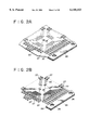
FIGS. 2A and 2B are perspective drawings showing the above embodiment in the order of processes;
FIG. 3 is a sectional view showing the main part of a semiconductor device using a lead frame in a transformed example of the above method of manufacturing the lead frame;
FIGS. 4A to 4E are sectional views showing processes (A) to (E) of processes (A) to (H) in order in a second embodiment of the method of manufacturing the lead frame according to the present invention;
FIGS. 5A to 5C are sectional views showing processes (F) to (H) of the processes (A) to (H) in order in the second embodiment of the method of manufacturing the lead frame according to the present invention;
FIG. 6 is a sectional view showing a semiconductor device installed using the lead frame in the second embodiment;
FIGS. 7A to 7H are sectional views showing a third embodiment of the method of manufacturing the lead frame according to the present invention in the order of processes;
FIGS. 8A to 8D show the assembly of the lead frame in the third embodiment and a semiconductor device in the order of processes;
FIG. 9 is a plan showing the semiconductor device installed using the lead frame in the third embodiment in a state in which sealant is removed;
FIGS. 10A to 10E are sectional views showing processes (A) to (E) of processes (A) to (H) in a conventional type method of manufacturing a lead frame in order;
FIGS. 11A to 11C are sectional views showing processes (F) to (H) of the processes (A) to (H) in the above conventional type in order;
FIG. 12 is a sectional view showing a semiconductor device installed using the lead frame in the conventional type example;
FIG. 13 shows an example of a mobile telephone out of electronic equipment; and
FIG. 14 shows a chip on lead in which a semiconductor device shown in FIG. 8 is reversed.
DESCRIPTION OF THE PREFERRED EMBODIMENTS
A first lead frame according to the present invention is characterized in that an etching stop layer provided between an outer lead and an inner lead composed of a thin wiring layer is formed by nickel or a nickel alloy and a second lead frame is characterized in that an etching stop layer between a lead composed of a thinmetal layer and an outside frame or an outside ring composed of thick metal is formed by nickel or a nickel alloy.
The thick metal layer constituting the outer lead and the outside ring or the outside frame is composed of copper or a copper alloy for example and formed so that the thick metal layer is 50 to 200 μm thick for example. The inner lead or a metal layer constituting leads is composed of copper or a copper alloy for example. The metal layer may be also directly formed on the etching stop layer composed of nickel or a nickel alloy, however, to enhance adhesion between the metal layer and the etching stop layer, thin copper 0.1 to 2.0 μm thick for example is plated on the etching stop layer and the metal layer may be also formed on the copper underplate layer.
The etching stop layer may be also formed by nickel, may be also formed by the other material such as a nickel alloy including phosphorous P for example and it is suitable that the thickness is set to approximately 0.1 to 5 μm.
A method of manufacturing the lead frame according to the present invention is characterized in that in the method of manufacturing the lead frame at least provided with an etching process for selectively etching metal layers using the etching stop layer as an etching stopper in a state in which a thick metal layer is formed on one side of the etching stop layer as an intermediate layer and a thin metal layer is formed on the other side and a process for etching the etching stop layer using the metal layers on both sides as a mask, the etching stop layer is formed by nickel or a nickel alloy. In the etching process for selectively etching the metal layers using the etching stop layer as an etching stopper, etchant the etching speed to nickel or a nickel alloy of which is slow and the etching speed to the metal layers formed on both sides of which is remarkably fast is naturally used. Any etchant may be also used if it is provided with such a property, however, if the metal layer is composed of copper or a copper alloy, for example, the mixed solution of aqueous ammonia the chemical formula of which is NH4 OH NH3 and the concentration of which is 15% or more for example and cupric chloride the chemical formula of which is CuCl2 and the density of which is 20% or more for example is suitable.
In the etching process for selectively etching the etching stop layer using the metal layers as an etching stopper, etchant the etching speed to the metal layers of which is slow and the etching speed to the etching stop layer composed of nickel or a nickel alloy as an intermediate layer of which is remarkably fast is naturally used. Any etchant may be also used if it is provided with such a property, however, if the metal layers are composed of copper or a copper alloy, process acidic liquid mainly composed of sulfuric acid of approximately 25% and hydrogen peroxide of approximately 6% for example is suitable.
Referring to the drawings, embodiments of the present invention will be described in detail below.
FIGS. 1A to 1E are sectional views showing a first embodiment of a method of manufacturing a lead frame according to the present invention in the order of processes and FIGS. 2A and 2B are perspective drawings showing the embodiment in the order of processes.
(A) As shown in FIG. 1A, a metal plate in which three layers are laminated is prepared as lead frame material 21. The lead frame material 21 is provided with three-layer structure in which an etching stop layer 22 with the thickness of 2 to 30 μm is held between a thick metal layer 23 composed of a 42% alloy or a copper base alloy with the thickness of approximately 100 to 250 μm for example and a thin metal layer 24 composed of copper foil with the thickness of approximately 10 to 50 μm. The thick metal layer 23 to be outer leads is provided to secure mechanical strength, while the thin metal layer 24 to be inner leads is formed thin so that a minute pattern can be formed.
The etching stop layer 22 is composed of nickel or a nickel alloy. As nickel or a nickel alloy is metal which is not etched by etchant for the metal layers 23 and 24, for example the mixed solution of aqueous ammonia the chemical formula of which is NH4 OH NH3 and the concentration of which is 15% or more for example and cupric chloride the chemical formula of which is CuCl2 and the density of which is 20% or more for example, the above metal is selected for the material of the etching stop layer 22, and the etching stop layer 22 plays a part of preventing one of the metal layers 23 and 24 from being etched by etching for the other later.
(B) Next, as shown in FIG. 1B, photo resist films 25a and 25b are respectively selectively formed on each surface of the metal layers 23 and 24. The photo resist film 25a formed on the surface of the thick metal layer 23 is provided with a pattern constituting a part except the inner lead of the lead frame and the photo resist film 25b formed on the surface of the thin metal layer 24 is provided with a pattern constituting a part to be particularly thick such as the inner lead and the vicinity of a guide hole 26. The width of an opening of the photo resist film 25 is normally set to 10 to 20 μm at the minimum, however, the width of an opening in a part to be thick such as the vicinity of the guide hole 26 is required to be set in consideration of the quantity of side etching.
(C) Next, the surface of the thick metal layer 23 of the lead frame material 1 is etched using for example the mixed solution of aqueous ammonia the chemical formula of which is NH4 OH NH3 and the concentration of which is 15% or more for example and cupric chloride the chemical formula of which is CuCl2 and the density of which is 20% or more for example. Then, as shown in FIG. 1C, the metal layer 23 is selectively etched and an outer lead 27 which is the body of the lead frame is formed.
(D) Next, the thin metal layer 24 is etched using the above etchant or sulfate to which fluoride salt and a surface active agent are added. Then, as shown in FIG. 1D, the metal layer 24 is selectively etched and a thick part 29 in which the inner lead 28 and the guide hole 6 are formed is formed. If the metal layer 24 is copper foil 18 μm thick, inner leads 28 can be actually formed at the pitch of approximately 40 μm which means remarkable fining and a request for increasing the number of pins can be met.
Afterward, the photo resist films 25a and 25b are removed by a solvent. FIG. 2A is a perspective drawing showing the state after the photo resist films 25a and 25b are removed.
(E) Next, the etching stop layer 22 is removed by etchant which is acid solution mainly composed of sulfuric acid of approximately 25% and hydrogen peroxide of approximately 6% for example. The etching speed of the etchant is slow to copper and is fast to nickel or a nickel alloy. As shown in FIG. 1E, after the etching, the etching stop layer 22 is left only in the part left after etching of the metal layer 23 and the metal layer 24, the etching stop layer 22 except that in the above part is removed and a lead frame is completed. FIG. 2B shows a state after the lead frame is completed.
If necessary, tin, gold, solder composed of lead of 10% and tin of 90% and others may be also plated overall or partly on the surface of the lead frame.
In the above example, the peeling of the photo resist films 25a and 25b and the removal of the etching stop layer 22 respectively after selective etching is finished are separately done, however, they may be also simultaneously done. If an ultrasonic wave is applied when the resists are removed, the resists can be readily removed.
According to this method of manufacturing a lead frame, the metal layer 23 of the lead frame material 21 can be formed so that the layer is thick enough to secure sufficient mechanical strength as the base metal (outer lead) of the lead frame and the metal layer 24 can be formed so that the layer is thin enough to form minute inner leads 28 by etching.
The reason is that as the etching stop layer 22 is held between the metal layers 23 and 24, the metal layers 23 and 24 can be independently etched.
Therefore, a lead frame provided with sufficient mechanical strength in which inner leads are minute can be obtained. Independent etching means not etching in separate processes but the etching of the metal layer 23 without having an effect upon the metal layer 24 or reverse etching. The etching of the metal layer 23 and the etching of the metal layer 24 can be also simultaneously executed.
Further, as the etching stop layer 22 is formed by nickel or a nickel alloy according to this embodiment, the etching stop layer 22 can be formed by plating. Therefore, as a high-priced vapor deposition device or sputtering device for vapor deposition or sputtering required in a case that aluminum is used for the etching stop layer 22 is not required, the cost of facilities can be reduced and as a result, the cost of a lead frame or a semiconductor device using it can be reduced.
As the etching stop layer 22 can be formed by plating, the adhesive strength of the etching stop layer 22 to each adjacent metal layer 27 and 28 can be enhanced, compared with a case that the etching stop layer is formed by vapor deposition or sputtering. The reason is that as the formation of a metal layer by plating is executed, growing a crystal lattice, stronger adhesive strength than adhesive strength by van der Waals force is remarkably obtained. Therefore, deterioration and peeling caused by the invasion of a chemical between the etching stop layer 22 and each adjacent metal layer 27 and 28 can be prevented.
FIG. 3 shows a semiconductor device using a lead frame in which a bump 30 composed of an etching stop layer 22 is formed at the end of an inner lead 28 by varying a part of the method shown in FIGS. 1. The lead frame can be formed by masking a part in which the bump 30 of the etching stop layer 22 is to be formed with a photo resist film again after metal layers 23 and 24 of lead frame material 21 are selectively etched and photo resist films 25a and 25b are removed according to the method of manufacturing the lead frame shown in FIGS. 1 and by etching the etching stop layer 22 afterward. Needless to say, the above method is not different from the embodiment shown in FIG. 1 as to the use of etchant. A reference number 41 in FIG. 3 denotes a semiconductor device, 41a denotes an electrode pad and 42 denotes resin.
FIGS. 4A to 4E and FIGS. 5A to 5C are sectional views showing a second embodiment of the method of manufacturing the lead frame according to the present invention in the order of processes (A) to (H).
(A) Lead frame material 31 with three-layer structure shown in FIG. 4A is prepared. The lead frame material 31 is formed by forming a nickel film 33 to be an etching stop layer approximately 3 μm thick for example by plating on the surface of a substrate 32 approximately 50 to 200 μm thick for example composed of copper or a copper alloy and further by forming an underplate layer 34 approximately 0.1 to 2 m thick for example composed of thin copper or nickel. The lead frame material 31 is an outside ring in a final process. The underplate layer 34 is formed to enhance the adhesiveness of leads described later and is not necessarily inevitable.
(B) Next, a resist film is formed on the above underplate layer 34 and is patterned by exposure and developing. The pattern of the resist film is negative to the pattern of leads to be formed. When above patterning is finished, a film composed of copper is plated using the resist film as a mask. A reference number 35 denotes a lead formed by plating and FIG. 4B shows a state after the resist film is removed after the lead 35 and others are formed. A laminate of metal films to be a lead may be also used for lead frame material and a lead may be also formed by etching the metal films.
(C) Next, as shown in FIG. 4C, a lead frame in which plural film circuits are integrated by selectively etching the lead frame material 31 from both sides so that the selective etching pierces a predetermined part of the lead frame material is formed. In etching, for example, the mixed solution of aqueous ammonia the chemical formula of which is NH4 OH NH3 and the concentration of which is 15% or more for example and cupric chloride the chemical formula of which is CuCl2 and the density of which is 20% or more for example is used for etchant.
(D) Next, as shown in FIG. 4D, an insulating layer (an insulating film) 36 is selectively formed on the surface of both sides to form a lead of the above lead frame material 31. A desired pattern is formed by applying the insulating layer 36 using resin material provided with photosensitivity, exposing and developing it. Reference numbers 37 denote an opening of the insulating layer 36 for exposing a part in which a ball electrode 38 of each lead 35 is to be formed and the insulating layer 36 is selectively etched to provide the openings 37.
(E) Next, as shown in FIG. 4E, solder balls 38 to be external terminals are formed on the surface of the above each lead 35 using the above insulating layer 36 as a mask. The solder balls 38 are formed by nickel plate 80 to 110 μm thick for example and solder or gold plate 0.1 to 5 μm thick for example or palladium.
(F) Next, as shown in FIG. 5A, a part inside a part 39 to be an outside ring of the thick copper layer 32 located on the rear side of the lead frame material 31 is removed by selectively etching from the rear side. In the above etching, the mixed solution of aqueous ammonia the chemical formula of which is NH4 OH NH3 and the concentration of which is 15% or more for example and cupric chloride the chemical formula of which is CuCl2 and the density of which is 20% or more for example is used for etchant. The reason is that the above etchant erodes copper, however, it does not erode nickel and nickel or a nickel alloy 33 can function as an etching stopper. In this process, nickel or a nickel alloy 33 is left except the part removed in the selective etching shown in FIG. 4C.
(G) Next, as shown in FIG. 5B, the underplate layer 34 under the leads 35 and the etching stop layer 33 which is an etching stopper are etched using the leads 35 and the left thick copper layer 32 as a mask. In the above etching, mixed solution mainly composed of sulfuric acid and hydrogen peroxide for example is used. Hereby, each lead 35 is separated and is released from a state in which each lead is mutually electrically short-circuited.
(H) Next, if necessary, as shown in FIG. 5C, a bump 40 is formed at the end of each lead 35. Therefore, a bump may be formed on the side of a semiconductor device 41 and no bump may be formed.
FIG. 6 is a sectional view showing a semiconductor device installed in the lead frame manufactured according to the method shown in FIGS. 4 and 5. A reference number 41 denotes a semiconductor device each electrode of which is connected to the end of the above each lead 35 via the bump 40. A reference number 42 denotes resin for sealing the semiconductor device 41, 43 denotes a thin dish-shaped heat spreader connected to each rear of the lead frame and the semiconductor device 41 and 44 denotes a conductive adhesive composed of silver paste for example for bonding the rear of the semiconductor device 41 to the heat spreader 43.
According to such a method of manufacturing the lead frame, as the etching stop layer 33 is formed by nickel or a nickel alloy, it can be formed by plating. Therefore, a high-priced vapor deposition device or a sputtering device required in a case that aluminum is used for the etching stop layer is not required. The cost of facilities can be reduced and as a result, the cost of a lead frame or a semiconductor device using it can be reduced.
As the etching stop layer 33 can be formed by plating, adhesive strength between the etching stop layer 33 and each adjacent metal layer 32 and 34 can be enhanced, compared with a case that the etching stop layer 33 is formed by vapor deposition or sputtering. Therefore, deterioration and peeling caused by the invasion of a chemical between the etching stop layer 3 and each adjacent metal layer can be prevented. Particularly, the change of the outside dimension of a package and the occurrence of a crack on the resin 42 for sealing, bonding and others respectively caused by the invasion of a chemical between the metal layer of the outside ring 39 and the etching stop layer 33 which is caused in a case that the outside ring 39 is provided and peeling as a result can be prevented.
FIGS. 7A to 7H are sectional views showing a third embodiment of the method of manufacturing the lead frame according to the present invention in the order of processes.
(A) First, as shown in FIG. 7A, lead frame material 51 composed of a metal laminated plate with three-layer structure is prepared. The lead frame material 51 is formed by laminating a copper layer 150 μm thick for example to be an outside ring for surrounding a semiconductor device and reinforcing it by adhesion to it, a nickel layer 63 with the thickness of 3 μm for example which functions as an etching stopper and is formed by plating and an underplate layer 64 composed of copper or nickel 2 μm thick for example. The underplate layer 64 may be also provided with multilayer structure such as a nickel layer 2 μm thick for example on a chromium layer 0.2 μm thick for example.
(B) Next, as shown in FIG. 7B, leads 53 and suspending parts 60 (The suspending parts 60 are not shown in FIG. 7. See FIG. 9.) are formed on the above underplate layer 64. Concretely, the leads and the suspending parts 60 are formed by applying resist according to the negative pattern of a pattern according to which the leads 53 and the suspending parts 60 are to be formed and plating copper or nickel so that it is 30 μm thick for example using the resist as a mask and using the layer 64 as underplate.
The suspending parts 60 are provided in the same layer as the leads 53 to suspend the outside ring 58 for reinforcement for surrounding the semiconductor device 41 and therefore, are composed of copper or nickel for example. In the meantime, the ring 58 is integrated outside the main part of the lead frame via the suspending parts 60 though the ring is not formed yet in this process and is provided with structure in which copper, aluminum, nickel and others are laminated.
(C) Next, as shown in FIG. 7C, a lead frame in which plural film circuits are integrated by selectively etching the metal laminate 51 from both sides so that selective etching pierces a predetermined part of the metal laminate is formed. In the above etching, for example etchant including ferric chloride composed of the mixed solution of aqueous ammonia the chemical formula of which is NH4 OH NH3 and the concentration of which is 15% or more for example and cupric chloride the chemical formula of which is CuCl2 and the density of which is 20% or more for example is used.
(D) Next, as shown in FIG. 7D, an insulating layer (an insulating film) 52 is selectively formed on the surface on the side on which leads are formed of the above laminate 51. Resin material provided with photosensitivity is used for the insulating layer 52 and a desired pattern is formed by applying, exposing and developing it. Reference number 61 denotes an opening of the insulating layer 52 for exposing a part in which ball electrode 56 of each lead 53 is to be formed and the insulating layer 52 is selectively etched so that the opening 61 is provided.
(E) Next, as shown in FIG. 7E, solder balls 56 to be external terminals are formed on the surface of each lead 53 using the insulating layer 52 as a mask. The solder balls 56 are formed by nickel plate 80 to 10 μm thick for example and solder or gold plate 0.1 to 5 μm thick for example or palladium.
(F) Next, as shown in FIG. 7F, a part inside a part 58 to be an outside ring of the thick copper layer 62 located on the rear side of the laminate 51 is removed by selectively etching from the rear side. In the above etching, etchant including ferric chloride composed of the mixed solution of aqueous ammonia the chemical formula of which is NH4 OH NH, and the concentration of which is 15% or more for example and cupric chloride the chemical formula of which is CuCl2 and the density of which is 20% or more for example is used. The reason is that the above etchant erodes copper, however, it does not erode nickel and a nickel layer 63 can function as an etching stopper.
In this process, the nickel layer 63 is left except the part removed in the selective etching shown in FIG. 7C.
(G) Next, as shown in FIG. 7G, the underplate layer 64 under the leads 53 and the etching stop layer 63 which is an etching stopper and composed of nickel or a nickel alloy are etched using the leads 53 and the suspending parts 60 (The suspending parts 60 are not shown in FIG. 7. See FIG. 9.) as a mask. In the above etching, the mixed solution of sulfuric acid and the solution of hydrogen peroxide for example is used. Hereby, each lead 53 and each suspending part 60 are separated and are released from a state in which they are mutually electrically short-circuited. A reference number 65 denotes the main part of the lead frame 51 and the main part 65 seems as if it were separated from the outside ring 58 in FIG. 7G, however, it is because the suspending parts 60 are not shown in the sectional view of FIG. 7G and actually, the main part is integrated with the outside ring 58 via the suspending parts 60.
(H) Next, if necessary, as shown in FIG. 7H, a bump 66 is formed at the end 53a of each lead 53. Therefore, a bump may be formed on the side of a semiconductor device 54 and no bump may be formed.
In this embodiment, the lead 53 is formed by growing a plate film using a resist film selectively formed on a underplate film as a mask, however, the lead may be also formed by forming a layer 64 composed of copper or nickel so that it is thick and patterning it by selective etching.
According to this embodiment, the lead frame 51 can be manufactured by utilizing a lead frame manufacturing method in which outer leads are formed on one side of a metal laminate provided with three-layer structure and inner leads are formed on the other side as the method is and as the base of the metal laminate 61 is composed of metal and rigidity is strong, minute leads 53 can be formed precisely and with high positioning precision.
As the etching stop layer 63 is formed by nickel or a nickel alloy, the etching stop layer 63 can be formed by plating. Therefore, a high-priced vapor deposition device or sputtering device for vapor deposition or sputtering required in a case that aluminum is used for the etching stop layer is not required. Therefore, the cost of facilities can be reduced and as a result, the cost of a lead frame or a semiconductor device using it can be reduced.
As the etching stop layer can be formed by plating, the adhesive strength of the etching stop layer 63 to the metal layer (outside ring) 58 can be enhanced, compared with a case that the etching stop layer is formed by vapor deposition or sputtering. Therefore, deterioration and peeling by the invasion of a chemical between the etching stop layer and the adjacent metal layer can be prevented.
FIGS. 8A to 8D show the assembly of the lead frame 51 the processes shown in FIG. 7 of which are finished and the semiconductor device 41 in the order of processes.
(A) First, as shown in FIG. 8A, the semiconductor device 41 aligned in the lead frame 51 is positioned and bonded via a buffer adhesive layer 57. As a buffer adhesive 57 bonds the lead frame 51 and the semiconductor device 41 and further, protects the surface of the semiconductor device 41, a property of cushioning is required.
(B) Next, as shown in FIG. 8B, the bump 66 at the end 3a of each lead 53 is connected to the electrode pad 55 of the semiconductor device 41 by single point bonding for example.
In this case, as the end of a part protruded from the insulating layer 52 of the lead 53 functions as a terminal on the side of the semiconductor device, the terminal is not required to be cut for bonding. In this point, the lead frame according to this present invention also differs from the conventional type. Therefore, time required for bonding can be reduced.
(C) Next, as shown in FIG. 8C, sealant 59 such as epoxy resin and silicon resin is injected between the semiconductor device 41 and the lead frame 51 and between them and the outside ring 58 by potting, seals and fixes between the semiconductor device 54 and the lead frame 51 and between them and the outside ring 58.
(D) Next, as shown in FIG. 8D, a part every semiconductor device of the lead frame 51 is mutually separated from another part by integrating leads for plural semiconductor devices 41 and cutting a unnecessary part of the lead frame 51. Hereby, a semiconductor device provided with the lead frame 51 as an intermediate circuit base, provided with external terminals 56 in a ball grid array respectively connected to each electrode of the semiconductor device on the intermediate circuit base and reinforced by the outside ring 58 can be obtained. FIG. 9 is a plan showing the semiconductor device formed as a result in a state in which the sealant 59 is removed.
According to this method of manufacturing the lead frame, as the etching stop layer 63 is formed by nickel or a nickel alloy, it can be formed by plating. Therefore, a high-priced vapor deposition device or sputtering device for vapor deposition or sputtering required in a case that aluminum is used for the etching stop layer is not required. Therefore, the cost of facilities can be reduced and as a result, the cost of a lead frame or a semiconductor device using it can be reduced.
As the etching stop layer can be formed by plating, the adhesive strength of the etching stop layer 63 to the metal layer (outside ring) 58 can be enhanced, compared with a case that the etching stop layer is formed by vapor deposition or sputtering. Therefore, deterioration and peeling caused by the invasion of a chemical between the etching stop layer and the adjacent metal layer can be prevented.
In the embodiment shown in FIGS. 4 and 5 and the embodiment shown in FIGS. 7, the etching stop layer composed of nickel or a nickel alloy is formed on the surface of the metal layer as the base material of the lead frame and the underplate layer composed of thin copper is formed on the etching stop layer to more enhance the adhesion of the metal layer composed of copper to be leads to the etching stop layer composed of nickel or a nickel alloy, however, if required adhesion is obtained without forming the underplate layer, the above underplate layer is not necessarily inevitable. If such an underplate layer is not formed, it is not required to be removed when leads are formed by selectively etching the metal layer and an advantage that a lead is never chipped due to the removal is produced.
As the above each semiconductor device can be manufactured at a low price as described above and the reliability is enhanced by electrically connecting an electrode on the circuit board and the external electrode of the above semiconductor device as shown in FIG. 14, it can be used for various electronic equipment, particularly, the above semiconductor device is used for a mobile telephone requiring miniaturization and others and greatly contributes to the miniaturization. FIG. 13 shows an example A of such electronic equipment such as a mobile telephone, the semiconductor device C according to the present invention is mounted on a circuit board B inside the electronic equipment shown as the example and functions at least as a part of the internal circuit of the electronic equipment.
According to the lead frame disclosed in claim 1, as the etching stop layer is formed by nickel or a nickel alloy, it can be formed by plating. Therefore, a high-priced vapor deposition device or sputtering device for vapor deposition or sputtering required in a case that aluminum is used for the etching stop layer is not required. Therefore, the cost of facilities can be reduced and as a result, the cost of a lead frame or a semiconductor device using it can be reduced.
As the etching stop layer can be formed by plating, the bonding strength of the etching stop layer to the adjacent metal layer can be enhanced, compared with a case that the etching stop layer is formed by vapor deposition or sputtering. Therefore, deterioration and peeling caused by the invasion of a chemical between the etching stop layer and the adjacent metal layer can be prevented.
According to the lead frame disclosed in claim 2, as the etching stop layer is formed by nickel or a nickel alloy, it can be formed by plating. Therefore, a high-priced vapor deposition device or sputtering device for vapor deposition or sputtering required in a case that aluminum is used for the etching stop layer is not required. Therefore, the cost of facilities can be reduced and as a result, the cost of a lead frame or a semiconductor device using it can be reduced.
As the etching stop layer can be formed by plating, the bonding strength of the etching stop layer to the adjacent metal layer can be enhanced, compared with a case that the etching stop layer is formed by vapor deposition or sputtering. Therefore, deterioration and peeling caused by the invasion of a chemical between the etching stop layer and the adjacent metal layer can be prevented. Particularly, the change of the outside dimension of a package and the occurrence of a crack on the resin for sealing, bonding and others respectively caused by the invasion of a chemical between the metal layer of the outside ring and the etching stop layer which is caused in a case that the outside ring is provided and peeling as a result can be prevented.
According to the method of manufacturing the lead frame disclosed in claim 3, as the etching stop layer is formed by nickel or an nickel alloy, it can be formed by plating. Therefore, a high-priced vapor deposition device or sputtering device for vapor deposition or sputtering required in a case that aluminum is used for the etching stop layer is not required. Therefore, the cost of facilities can be reduced and as a result, the cost of a lead frame or a semiconductor device using it can be reduced.
As the etching stop layer can be formed by plating, the bonding strength of the etching stop layer to the adjacent metal layer can be enhanced, compared with a case that the etching stop layer is formed by vapor deposition or sputtering. Therefore, deterioration and peeling caused by the invasion of a chemical between the etching stop layer and the adjacent metal layer can be prevented.
According to the semiconductor device disclosed in claim 4, as the etching stop layer of the lead frame used for installing the semiconductor device is formed by nickel or a nickel alloy, the semiconductor device can receive the above advantages with which such a lead frame is provided.
According to the method of manufacturing the semiconductor device disclosed in claim 5, as the semiconductor device is manufactured using the lead frame in which the etching stop layer is formed by nickel or a nickel alloy, the method of manufacturing the semiconductor device can receive the above advantages with which such a lead frame is provided.

Claims (7)

What is claimed is:
1. A method of manufacturing a lead frame, said method comprising the steps of:
a process for forming an etching stop layer comprising one of nickel and a nickel alloy on a first metal layer;
a process for forming plural leads from a second metal layer formed on said etching stop layer;
a process for forming an insulating layer on said plural leads, said insulating layer having openings between said plural leads;
a process for selectively etching said first metal layer using said etching stop layer as a stopper; and
a process for etching said etching stop layer using said plural leads and an unetched part of said first metal layer as a mask.
2. A method of manufacturing a lead frame according to claim 1, wherein:
said etching stop layer is formed by plating nickel or a nickel alloy.
3. A method of manufacturing a lead frame according to claim 1, wherein:
said insulating layer embeds said plural leads; and
the surface on the side on which a semiconductor device is located of said lead frame is a plane composed of said insulating layer and said plural leads.
4. A method of manufacturing a lead frame according to claim 1, wherein:
a process for forming an external electrode at said plural openings is further included.
5. A method of manufacturing a lead frame according to claim 1, wherein:
said plural leads are formed by plating.
6. A method of manufacturing a lead frame according to claim 1, wherein:
an underplate metal layer is formed on said etching stop layer.
7. A lead frame, wherein:
plural leads are formed on a same surface of said lead frame on which a semiconductor device is located:
an insulating layer is formed on and between said plural leads, said insulating layer having plural openings formed therethrough for respectively exposing said plural leads;
an external electrode is formed at each of said openings;
an outside ring comprising a metal layer thicker than said plural leads is provided at a periphery of a part in which said plural leads are provided and connected to said part via a suspending part; and
said outside ring comprises a metal lamination having an etching stop layer comprising one of nickel and a nickel alloy formed on a side adjacent said suspending part.
US09/084,189 1997-05-27 1998-05-26 Lead frame, the manufacturing method, semiconductor device and the manufacturing method Expired - Fee Related US6140153A (en)

Priority Applications (3)

Application Number Priority Date Filing Date Title
US09/702,456 US6403402B1 (en) 1997-05-27 2000-10-31 Semiconductor chip having an underplate metal layer
US09/702,437 US6369441B1 (en) 1997-05-27 2000-10-31 Method of producing a semiconductor chip having an underplate metal layer
US09/702,457 US6351025B1 (en) 1997-05-27 2000-10-31 Semiconductor chip having an underplate metal layer

Applications Claiming Priority (2)

Application Number Priority Date Filing Date Title
JP9-136776 1997-05-27
JP9136776A JP3003624B2 (en) 1997-05-27 1997-05-27 Semiconductor device

Related Child Applications (4)

Application Number Title Priority Date Filing Date
US29091359 Continuation-In-Part 1998-07-28
US09/702,437 Division US6369441B1 (en) 1997-05-27 2000-10-31 Method of producing a semiconductor chip having an underplate metal layer
US09/702,457 Division US6351025B1 (en) 1997-05-27 2000-10-31 Semiconductor chip having an underplate metal layer
US09/702,456 Division US6403402B1 (en) 1997-05-27 2000-10-31 Semiconductor chip having an underplate metal layer

Publications (1)

Publication Number Publication Date
US6140153A true US6140153A (en) 2000-10-31

Family

ID=15183260

Family Applications (4)

Application Number Title Priority Date Filing Date
US09/084,189 Expired - Fee Related US6140153A (en) 1997-05-27 1998-05-26 Lead frame, the manufacturing method, semiconductor device and the manufacturing method
US09/702,457 Expired - Fee Related US6351025B1 (en) 1997-05-27 2000-10-31 Semiconductor chip having an underplate metal layer
US09/702,456 Expired - Fee Related US6403402B1 (en) 1997-05-27 2000-10-31 Semiconductor chip having an underplate metal layer
US09/702,437 Expired - Fee Related US6369441B1 (en) 1997-05-27 2000-10-31 Method of producing a semiconductor chip having an underplate metal layer

Family Applications After (3)

Application Number Title Priority Date Filing Date
US09/702,457 Expired - Fee Related US6351025B1 (en) 1997-05-27 2000-10-31 Semiconductor chip having an underplate metal layer
US09/702,456 Expired - Fee Related US6403402B1 (en) 1997-05-27 2000-10-31 Semiconductor chip having an underplate metal layer
US09/702,437 Expired - Fee Related US6369441B1 (en) 1997-05-27 2000-10-31 Method of producing a semiconductor chip having an underplate metal layer

Country Status (5)

Country Link
US (4) US6140153A (en)
JP (1) JP3003624B2 (en)
KR (1) KR100563177B1 (en)
SG (1) SG68051A1 (en)
TW (1) TW379429B (en)

Cited By (5)

* Cited by examiner, † Cited by third party
Publication number Priority date Publication date Assignee Title
US6369441B1 (en) * 1997-05-27 2002-04-09 Sony Corporation Method of producing a semiconductor chip having an underplate metal layer
US6663980B1 (en) * 1998-09-30 2003-12-16 Toyo Kohan Co., Ltd. Clad plate for lead frames, lead frame using the same, and method of manufacturing the lead frame
US20050263871A1 (en) * 2004-05-20 2005-12-01 Yasuhiro Shinma Method of fabricating semiconductor device and semiconductor device
US8008130B2 (en) * 1999-10-05 2011-08-30 Renesas Electronics Corporation Multilayer interconnection board, semiconductor device having the same, and method of forming the same as well as method of mounting the semicondutor chip on the interconnection board
US9537065B2 (en) 2011-08-12 2017-01-03 Sharp Kabushiki Kaisha Light-emitting device with reflective resin

Families Citing this family (14)

* Cited by examiner, † Cited by third party
Publication number Priority date Publication date Assignee Title
JP2001230360A (en) * 2000-02-18 2001-08-24 Hitachi Ltd Semiconductor integrated circuit device and method of manufacturing the same
US6479893B2 (en) * 2000-12-04 2002-11-12 Semiconductor Components Industries Llc Ball-less clip bonding
JP2002261190A (en) * 2001-02-28 2002-09-13 Sony Corp Semiconductor device, method for manufacturing the same and electronic equipment
WO2003085728A1 (en) * 2002-04-11 2003-10-16 Koninklijke Philips Electronics N.V. Carrier, method of manufacturing a carrier and an electronic device
CN101317267B (en) * 2005-09-30 2010-09-08 Nxp股份有限公司 System-in-package (SIP) device based on fine-pitch routing in a lead frame
DE602006020179D1 (en) 2005-11-28 2011-03-31 Nxp Bv RANSPONDER
US7371616B2 (en) * 2006-01-05 2008-05-13 Fairchild Semiconductor Corporation Clipless and wireless semiconductor die package and method for making the same
US20080298024A1 (en) * 2007-05-31 2008-12-04 A.L.M.T. Corp. Heat spreader and method for manufacturing the same, and semiconductor device
KR101204092B1 (en) 2008-05-16 2012-11-22 삼성테크윈 주식회사 Lead frame and semiconductor package and the manufacturing method for the same
US8551820B1 (en) 2009-09-28 2013-10-08 Amkor Technology, Inc. Routable single layer substrate and semiconductor package including same
US9911685B2 (en) 2012-11-09 2018-03-06 Amkor Technology, Inc. Land structure for semiconductor package and method therefor
KR20140060390A (en) 2012-11-09 2014-05-20 앰코 테크놀로지 코리아 주식회사 Land structure for semiconductor package and manufacturing method thereof, semiconductor package and manufacturing method thereof
US10529672B2 (en) 2017-08-31 2020-01-07 Stmicroelectronics, Inc. Package with interlocking leads and manufacturing the same
US11887916B2 (en) 2020-09-09 2024-01-30 Amkor Technology Singapore Holding Pte. Ltd. Semiconductor devices and methods of manufacturing semiconductor devices

Citations (17)

* Cited by examiner, † Cited by third party
Publication number Priority date Publication date Assignee Title
US4967313A (en) * 1988-07-15 1990-10-30 Contraves Ag Electronic circuit and method of production thereof
US5221428A (en) * 1989-11-06 1993-06-22 Sony Corporation Production of lead frame
US5359222A (en) * 1992-01-31 1994-10-25 Kabushiki Kaisha Toshiba TCP type semiconductor device capable of preventing crosstalk
US5422514A (en) * 1993-05-11 1995-06-06 Micromodule Systems, Inc. Packaging and interconnect system for integrated circuits
US5437764A (en) * 1993-05-25 1995-08-01 Sony Corporation Lead frame and manufacturing method therefor
US5474957A (en) * 1994-05-09 1995-12-12 Nec Corporation Process of mounting tape automated bonded semiconductor chip on printed circuit board through bumps
US5481798A (en) * 1994-01-19 1996-01-09 Sony Corporation Etching method for forming a lead frame
US5541447A (en) * 1992-04-22 1996-07-30 Yamaha Corporation Lead frame
US5656550A (en) * 1994-08-24 1997-08-12 Fujitsu Limited Method of producing a semicondutor device having a lead portion with outer connecting terminal
US5756377A (en) * 1994-11-22 1998-05-26 Sony Corporation Lead frame and manufacturing method thereof
WO1998034278A1 (en) * 1997-02-03 1998-08-06 Nippon Denkai, Ltd. Lead frame material
US5843810A (en) * 1996-02-06 1998-12-01 Sony Corporation Film circuit and method of manufacturing the same
US5886399A (en) * 1995-09-20 1999-03-23 Sony Corporation Lead frame and integrated circuit package
US5945741A (en) * 1995-11-21 1999-08-31 Sony Corporation Semiconductor chip housing having a reinforcing plate
US5982033A (en) * 1995-09-20 1999-11-09 Sony Corporation Semiconductor chip package
US6020626A (en) * 1997-09-19 2000-02-01 Sony Corporation Semiconductor device
US6051450A (en) * 1997-07-01 2000-04-18 Sony Corporation Lead frame, manufacturing method of a lead frame, semiconductor device, assembling method of a semiconductor device, and electronic apparatus

Family Cites Families (8)

* Cited by examiner, † Cited by third party
Publication number Priority date Publication date Assignee Title
JP2861841B2 (en) * 1994-11-22 1999-02-24 ソニー株式会社 Lead frame manufacturing method
JP3422144B2 (en) * 1995-09-22 2003-06-30 ソニー株式会社 Semiconductor package manufacturing method
JPH09312374A (en) * 1996-05-24 1997-12-02 Sony Corp Semiconductor package and manufacture thereof
SG60099A1 (en) * 1996-08-16 1999-02-22 Sony Corp Semiconductor package and manufacturing method of lead frame
US6074898A (en) * 1996-09-18 2000-06-13 Sony Corporation Lead frame and integrated circuit package
US5937278A (en) * 1996-10-15 1999-08-10 Sony Corporation Method of manufacturing lead frame having inner lead connected to outer lead by metal etch stop layer
JPH10326795A (en) * 1997-03-28 1998-12-08 Sony Corp Semiconductor device and its manufacture
JP3003624B2 (en) * 1997-05-27 2000-01-31 ソニー株式会社 Semiconductor device

Patent Citations (18)

* Cited by examiner, † Cited by third party
Publication number Priority date Publication date Assignee Title
US4967313A (en) * 1988-07-15 1990-10-30 Contraves Ag Electronic circuit and method of production thereof
US5221428A (en) * 1989-11-06 1993-06-22 Sony Corporation Production of lead frame
US5659198A (en) * 1992-01-31 1997-08-19 Kabushiki Kaisha Toshiba TCP type semiconductor device capable of preventing crosstalk
US5359222A (en) * 1992-01-31 1994-10-25 Kabushiki Kaisha Toshiba TCP type semiconductor device capable of preventing crosstalk
US5541447A (en) * 1992-04-22 1996-07-30 Yamaha Corporation Lead frame
US5422514A (en) * 1993-05-11 1995-06-06 Micromodule Systems, Inc. Packaging and interconnect system for integrated circuits
US5437764A (en) * 1993-05-25 1995-08-01 Sony Corporation Lead frame and manufacturing method therefor
US5481798A (en) * 1994-01-19 1996-01-09 Sony Corporation Etching method for forming a lead frame
US5474957A (en) * 1994-05-09 1995-12-12 Nec Corporation Process of mounting tape automated bonded semiconductor chip on printed circuit board through bumps
US5656550A (en) * 1994-08-24 1997-08-12 Fujitsu Limited Method of producing a semicondutor device having a lead portion with outer connecting terminal
US5756377A (en) * 1994-11-22 1998-05-26 Sony Corporation Lead frame and manufacturing method thereof
US5886399A (en) * 1995-09-20 1999-03-23 Sony Corporation Lead frame and integrated circuit package
US5982033A (en) * 1995-09-20 1999-11-09 Sony Corporation Semiconductor chip package
US5945741A (en) * 1995-11-21 1999-08-31 Sony Corporation Semiconductor chip housing having a reinforcing plate
US5843810A (en) * 1996-02-06 1998-12-01 Sony Corporation Film circuit and method of manufacturing the same
WO1998034278A1 (en) * 1997-02-03 1998-08-06 Nippon Denkai, Ltd. Lead frame material
US6051450A (en) * 1997-07-01 2000-04-18 Sony Corporation Lead frame, manufacturing method of a lead frame, semiconductor device, assembling method of a semiconductor device, and electronic apparatus
US6020626A (en) * 1997-09-19 2000-02-01 Sony Corporation Semiconductor device

Cited By (7)

* Cited by examiner, † Cited by third party
Publication number Priority date Publication date Assignee Title
US6369441B1 (en) * 1997-05-27 2002-04-09 Sony Corporation Method of producing a semiconductor chip having an underplate metal layer
US6403402B1 (en) * 1997-05-27 2002-06-11 Sony Corporation Semiconductor chip having an underplate metal layer
US6663980B1 (en) * 1998-09-30 2003-12-16 Toyo Kohan Co., Ltd. Clad plate for lead frames, lead frame using the same, and method of manufacturing the lead frame
US8008130B2 (en) * 1999-10-05 2011-08-30 Renesas Electronics Corporation Multilayer interconnection board, semiconductor device having the same, and method of forming the same as well as method of mounting the semicondutor chip on the interconnection board
US20050263871A1 (en) * 2004-05-20 2005-12-01 Yasuhiro Shinma Method of fabricating semiconductor device and semiconductor device
US9368424B2 (en) * 2004-05-20 2016-06-14 Cypress Semiconductor Corporation Method of fabricating a semiconductor device used in a stacked-type semiconductor device
US9537065B2 (en) 2011-08-12 2017-01-03 Sharp Kabushiki Kaisha Light-emitting device with reflective resin

Also Published As

Publication number Publication date
JPH10335569A (en) 1998-12-18
KR100563177B1 (en) 2006-05-25
SG68051A1 (en) 1999-10-19
US6403402B1 (en) 2002-06-11
TW379429B (en) 2000-01-11
US6369441B1 (en) 2002-04-09
US6351025B1 (en) 2002-02-26
JP3003624B2 (en) 2000-01-31
KR19980087404A (en) 1998-12-05

Similar Documents

Publication Publication Date Title
US6140153A (en) Lead frame, the manufacturing method, semiconductor device and the manufacturing method
US7115818B2 (en) Flexible multilayer wiring board and manufacture method thereof
US8230591B2 (en) Method for fabricating an electronic device substrate
KR100346630B1 (en) Lead frame and manufacturing method
US7939935B2 (en) Electronic device substrate, electronic device and methods for fabricating the same
KR100551173B1 (en) Flip chip type semiconductor device and method of manufacturing the same
US7530163B2 (en) Electronic parts packaging structure and method of manufacturing the same
KR100437437B1 (en) Semiconductor package manufacturing method and semiconductor package
KR100834657B1 (en) Electronic device substrate and its fabrication method, and electronic device and its fabrication method
JPH1174413A (en) Lead frame and its manufacture, semiconductor device and its assembling method, and electronic equipment
WO2004100260A1 (en) High-density multi-layered printed wiring board, multi-chip carrier, and semiconductor package
US6593224B1 (en) Method of manufacturing a multilayer interconnect substrate
US20200305289A1 (en) Flexible substrate and method for fabricating the same
KR100679470B1 (en) Lead frame and production method thereof, and semiconductor device and fabrication method thereof
JP3981227B2 (en) Multilayer wiring board and manufacturing method thereof
JP4110391B2 (en) WIRING BOARD AND METHOD FOR MANUFACTURING SAME, SEMICONDUCTOR DEVICE, ELECTRONIC MODULE, AND ELECTRONIC DEVICE
JP2005235982A (en) Wiring substrate and its manufacturing method, and semiconductor package
JP2000077573A (en) Lead frame, its manufacture and manufacture of semiconductor device
KR100708042B1 (en) Manufacturing method of substrate for semiconductor package
JP2002343818A (en) Bga wiring substrate, manufacturing method therefor and method of manufacturing semiconductor device
JP2001110931A (en) Manufacturing method of 2-layer metal film carrier
JP2005235980A (en) Wiring substrate and its manufacturing method, and semiconductor package
JP2000277652A (en) Semiconductor package
KR20090011932A (en) Method of manufacturing substrate using a semiconductor package
JP2004259776A (en) Circuit substrate and its manufacturing method

Legal Events

Date Code Title Description
AS Assignment

Owner name: SONY CORPORATION, JAPAN

Free format text: ASSIGNMENT OF ASSIGNORS INTEREST;ASSIGNORS:OHSAWA, KENJI;KUSANO, HIDETOSHI;REEL/FRAME:009302/0193

Effective date: 19980629

FPAY Fee payment

Year of fee payment: 4

FPAY Fee payment

Year of fee payment: 8

REMI Maintenance fee reminder mailed
FEPP Fee payment procedure

Free format text: PAYER NUMBER DE-ASSIGNED (ORIGINAL EVENT CODE: RMPN); ENTITY STATUS OF PATENT OWNER: LARGE ENTITY

Free format text: PAYOR NUMBER ASSIGNED (ORIGINAL EVENT CODE: ASPN); ENTITY STATUS OF PATENT OWNER: LARGE ENTITY

REMI Maintenance fee reminder mailed
LAPS Lapse for failure to pay maintenance fees
STCH Information on status: patent discontinuation

Free format text: PATENT EXPIRED DUE TO NONPAYMENT OF MAINTENANCE FEES UNDER 37 CFR 1.362

FP Lapsed due to failure to pay maintenance fee

Effective date: 20121031