US6143581A - Asymmetric transfer molding method and an asymmetric encapsulation made therefrom - Google Patents
Asymmetric transfer molding method and an asymmetric encapsulation made therefrom Download PDFInfo
- Publication number
- US6143581A US6143581A US09/255,554 US25555499A US6143581A US 6143581 A US6143581 A US 6143581A US 25555499 A US25555499 A US 25555499A US 6143581 A US6143581 A US 6143581A
- Authority
- US
- United States
- Prior art keywords
- molding
- section
- filling
- flexible substrate
- electrical device
- Prior art date
- Legal status (The legal status is an assumption and is not a legal conclusion. Google has not performed a legal analysis and makes no representation as to the accuracy of the status listed.)
- Expired - Lifetime
Links
Images


Classifications
-
- H—ELECTRICITY
- H01—ELECTRIC ELEMENTS
- H01L—SEMICONDUCTOR DEVICES NOT COVERED BY CLASS H10
- H01L23/00—Details of semiconductor or other solid state devices
- H01L23/28—Encapsulations, e.g. encapsulating layers, coatings, e.g. for protection
- H01L23/29—Encapsulations, e.g. encapsulating layers, coatings, e.g. for protection characterised by the material, e.g. carbon
- H01L23/293—Organic, e.g. plastic
-
- B—PERFORMING OPERATIONS; TRANSPORTING
- B29—WORKING OF PLASTICS; WORKING OF SUBSTANCES IN A PLASTIC STATE IN GENERAL
- B29C—SHAPING OR JOINING OF PLASTICS; SHAPING OF MATERIAL IN A PLASTIC STATE, NOT OTHERWISE PROVIDED FOR; AFTER-TREATMENT OF THE SHAPED PRODUCTS, e.g. REPAIRING
- B29C45/00—Injection moulding, i.e. forcing the required volume of moulding material through a nozzle into a closed mould; Apparatus therefor
- B29C45/14—Injection moulding, i.e. forcing the required volume of moulding material through a nozzle into a closed mould; Apparatus therefor incorporating preformed parts or layers, e.g. injection moulding around inserts or for coating articles
- B29C45/14336—Coating a portion of the article, e.g. the edge of the article
- B29C45/14418—Sealing means between mould and article
-
- B—PERFORMING OPERATIONS; TRANSPORTING
- B29—WORKING OF PLASTICS; WORKING OF SUBSTANCES IN A PLASTIC STATE IN GENERAL
- B29C—SHAPING OR JOINING OF PLASTICS; SHAPING OF MATERIAL IN A PLASTIC STATE, NOT OTHERWISE PROVIDED FOR; AFTER-TREATMENT OF THE SHAPED PRODUCTS, e.g. REPAIRING
- B29C45/00—Injection moulding, i.e. forcing the required volume of moulding material through a nozzle into a closed mould; Apparatus therefor
- B29C45/14—Injection moulding, i.e. forcing the required volume of moulding material through a nozzle into a closed mould; Apparatus therefor incorporating preformed parts or layers, e.g. injection moulding around inserts or for coating articles
- B29C45/14639—Injection moulding, i.e. forcing the required volume of moulding material through a nozzle into a closed mould; Apparatus therefor incorporating preformed parts or layers, e.g. injection moulding around inserts or for coating articles for obtaining an insulating effect, e.g. for electrical components
- B29C45/14655—Injection moulding, i.e. forcing the required volume of moulding material through a nozzle into a closed mould; Apparatus therefor incorporating preformed parts or layers, e.g. injection moulding around inserts or for coating articles for obtaining an insulating effect, e.g. for electrical components connected to or mounted on a carrier, e.g. lead frame
-
- H—ELECTRICITY
- H01—ELECTRIC ELEMENTS
- H01L—SEMICONDUCTOR DEVICES NOT COVERED BY CLASS H10
- H01L21/00—Processes or apparatus adapted for the manufacture or treatment of semiconductor or solid state devices or of parts thereof
- H01L21/02—Manufacture or treatment of semiconductor devices or of parts thereof
- H01L21/04—Manufacture or treatment of semiconductor devices or of parts thereof the devices having at least one potential-jump barrier or surface barrier, e.g. PN junction, depletion layer or carrier concentration layer
- H01L21/50—Assembly of semiconductor devices using processes or apparatus not provided for in a single one of the subgroups H01L21/06 - H01L21/326, e.g. sealing of a cap to a base of a container
- H01L21/56—Encapsulations, e.g. encapsulation layers, coatings
- H01L21/565—Moulds
-
- H—ELECTRICITY
- H01—ELECTRIC ELEMENTS
- H01L—SEMICONDUCTOR DEVICES NOT COVERED BY CLASS H10
- H01L23/00—Details of semiconductor or other solid state devices
- H01L23/28—Encapsulations, e.g. encapsulating layers, coatings, e.g. for protection
- H01L23/31—Encapsulations, e.g. encapsulating layers, coatings, e.g. for protection characterised by the arrangement or shape
- H01L23/3107—Encapsulations, e.g. encapsulating layers, coatings, e.g. for protection characterised by the arrangement or shape the device being completely enclosed
- H01L23/3121—Encapsulations, e.g. encapsulating layers, coatings, e.g. for protection characterised by the arrangement or shape the device being completely enclosed a substrate forming part of the encapsulation
-
- B—PERFORMING OPERATIONS; TRANSPORTING
- B29—WORKING OF PLASTICS; WORKING OF SUBSTANCES IN A PLASTIC STATE IN GENERAL
- B29C—SHAPING OR JOINING OF PLASTICS; SHAPING OF MATERIAL IN A PLASTIC STATE, NOT OTHERWISE PROVIDED FOR; AFTER-TREATMENT OF THE SHAPED PRODUCTS, e.g. REPAIRING
- B29C45/00—Injection moulding, i.e. forcing the required volume of moulding material through a nozzle into a closed mould; Apparatus therefor
- B29C45/14—Injection moulding, i.e. forcing the required volume of moulding material through a nozzle into a closed mould; Apparatus therefor incorporating preformed parts or layers, e.g. injection moulding around inserts or for coating articles
- B29C45/14639—Injection moulding, i.e. forcing the required volume of moulding material through a nozzle into a closed mould; Apparatus therefor incorporating preformed parts or layers, e.g. injection moulding around inserts or for coating articles for obtaining an insulating effect, e.g. for electrical components
- B29C45/14655—Injection moulding, i.e. forcing the required volume of moulding material through a nozzle into a closed mould; Apparatus therefor incorporating preformed parts or layers, e.g. injection moulding around inserts or for coating articles for obtaining an insulating effect, e.g. for electrical components connected to or mounted on a carrier, e.g. lead frame
- B29C2045/14672—Injection moulding, i.e. forcing the required volume of moulding material through a nozzle into a closed mould; Apparatus therefor incorporating preformed parts or layers, e.g. injection moulding around inserts or for coating articles for obtaining an insulating effect, e.g. for electrical components connected to or mounted on a carrier, e.g. lead frame moulding with different depths of the upper and lower mould cavity
-
- H—ELECTRICITY
- H01—ELECTRIC ELEMENTS
- H01L—SEMICONDUCTOR DEVICES NOT COVERED BY CLASS H10
- H01L2224/00—Indexing scheme for arrangements for connecting or disconnecting semiconductor or solid-state bodies and methods related thereto as covered by H01L24/00
- H01L2224/01—Means for bonding being attached to, or being formed on, the surface to be connected, e.g. chip-to-package, die-attach, "first-level" interconnects; Manufacturing methods related thereto
- H01L2224/02—Bonding areas; Manufacturing methods related thereto
- H01L2224/04—Structure, shape, material or disposition of the bonding areas prior to the connecting process
- H01L2224/05—Structure, shape, material or disposition of the bonding areas prior to the connecting process of an individual bonding area
- H01L2224/0554—External layer
- H01L2224/05599—Material
-
- H—ELECTRICITY
- H01—ELECTRIC ELEMENTS
- H01L—SEMICONDUCTOR DEVICES NOT COVERED BY CLASS H10
- H01L2224/00—Indexing scheme for arrangements for connecting or disconnecting semiconductor or solid-state bodies and methods related thereto as covered by H01L24/00
- H01L2224/01—Means for bonding being attached to, or being formed on, the surface to be connected, e.g. chip-to-package, die-attach, "first-level" interconnects; Manufacturing methods related thereto
- H01L2224/42—Wire connectors; Manufacturing methods related thereto
- H01L2224/47—Structure, shape, material or disposition of the wire connectors after the connecting process
- H01L2224/48—Structure, shape, material or disposition of the wire connectors after the connecting process of an individual wire connector
- H01L2224/481—Disposition
- H01L2224/48151—Connecting between a semiconductor or solid-state body and an item not being a semiconductor or solid-state body, e.g. chip-to-substrate, chip-to-passive
- H01L2224/48221—Connecting between a semiconductor or solid-state body and an item not being a semiconductor or solid-state body, e.g. chip-to-substrate, chip-to-passive the body and the item being stacked
- H01L2224/48225—Connecting between a semiconductor or solid-state body and an item not being a semiconductor or solid-state body, e.g. chip-to-substrate, chip-to-passive the body and the item being stacked the item being non-metallic, e.g. insulating substrate with or without metallisation
- H01L2224/4824—Connecting between the body and an opposite side of the item with respect to the body
-
- H—ELECTRICITY
- H01—ELECTRIC ELEMENTS
- H01L—SEMICONDUCTOR DEVICES NOT COVERED BY CLASS H10
- H01L2224/00—Indexing scheme for arrangements for connecting or disconnecting semiconductor or solid-state bodies and methods related thereto as covered by H01L24/00
- H01L2224/80—Methods for connecting semiconductor or other solid state bodies using means for bonding being attached to, or being formed on, the surface to be connected
- H01L2224/85—Methods for connecting semiconductor or other solid state bodies using means for bonding being attached to, or being formed on, the surface to be connected using a wire connector
- H01L2224/8538—Bonding interfaces outside the semiconductor or solid-state body
- H01L2224/85399—Material
-
- H—ELECTRICITY
- H01—ELECTRIC ELEMENTS
- H01L—SEMICONDUCTOR DEVICES NOT COVERED BY CLASS H10
- H01L24/00—Arrangements for connecting or disconnecting semiconductor or solid-state bodies; Methods or apparatus related thereto
- H01L24/01—Means for bonding being attached to, or being formed on, the surface to be connected, e.g. chip-to-package, die-attach, "first-level" interconnects; Manufacturing methods related thereto
- H01L24/42—Wire connectors; Manufacturing methods related thereto
- H01L24/47—Structure, shape, material or disposition of the wire connectors after the connecting process
- H01L24/48—Structure, shape, material or disposition of the wire connectors after the connecting process of an individual wire connector
-
- H—ELECTRICITY
- H01—ELECTRIC ELEMENTS
- H01L—SEMICONDUCTOR DEVICES NOT COVERED BY CLASS H10
- H01L2924/00—Indexing scheme for arrangements or methods for connecting or disconnecting semiconductor or solid-state bodies as covered by H01L24/00
- H01L2924/0001—Technical content checked by a classifier
- H01L2924/00014—Technical content checked by a classifier the subject-matter covered by the group, the symbol of which is combined with the symbol of this group, being disclosed without further technical details
-
- H—ELECTRICITY
- H01—ELECTRIC ELEMENTS
- H01L—SEMICONDUCTOR DEVICES NOT COVERED BY CLASS H10
- H01L2924/00—Indexing scheme for arrangements or methods for connecting or disconnecting semiconductor or solid-state bodies as covered by H01L24/00
- H01L2924/10—Details of semiconductor or other solid state devices to be connected
- H01L2924/11—Device type
- H01L2924/14—Integrated circuits
- H01L2924/143—Digital devices
- H01L2924/1433—Application-specific integrated circuit [ASIC]
-
- H—ELECTRICITY
- H01—ELECTRIC ELEMENTS
- H01L—SEMICONDUCTOR DEVICES NOT COVERED BY CLASS H10
- H01L2924/00—Indexing scheme for arrangements or methods for connecting or disconnecting semiconductor or solid-state bodies as covered by H01L24/00
- H01L2924/15—Details of package parts other than the semiconductor or other solid state devices to be connected
- H01L2924/151—Die mounting substrate
- H01L2924/153—Connection portion
- H01L2924/1531—Connection portion the connection portion being formed only on the surface of the substrate opposite to the die mounting surface
- H01L2924/15311—Connection portion the connection portion being formed only on the surface of the substrate opposite to the die mounting surface being a ball array, e.g. BGA
-
- H—ELECTRICITY
- H01—ELECTRIC ELEMENTS
- H01L—SEMICONDUCTOR DEVICES NOT COVERED BY CLASS H10
- H01L2924/00—Indexing scheme for arrangements or methods for connecting or disconnecting semiconductor or solid-state bodies as covered by H01L24/00
- H01L2924/15—Details of package parts other than the semiconductor or other solid state devices to be connected
- H01L2924/181—Encapsulation
-
- Y—GENERAL TAGGING OF NEW TECHNOLOGICAL DEVELOPMENTS; GENERAL TAGGING OF CROSS-SECTIONAL TECHNOLOGIES SPANNING OVER SEVERAL SECTIONS OF THE IPC; TECHNICAL SUBJECTS COVERED BY FORMER USPC CROSS-REFERENCE ART COLLECTIONS [XRACs] AND DIGESTS
- Y10—TECHNICAL SUBJECTS COVERED BY FORMER USPC
- Y10T—TECHNICAL SUBJECTS COVERED BY FORMER US CLASSIFICATION
- Y10T428/00—Stock material or miscellaneous articles
- Y10T428/13—Hollow or container type article [e.g., tube, vase, etc.]
- Y10T428/1352—Polymer or resin containing [i.e., natural or synthetic]
-
- Y—GENERAL TAGGING OF NEW TECHNOLOGICAL DEVELOPMENTS; GENERAL TAGGING OF CROSS-SECTIONAL TECHNOLOGIES SPANNING OVER SEVERAL SECTIONS OF THE IPC; TECHNICAL SUBJECTS COVERED BY FORMER USPC CROSS-REFERENCE ART COLLECTIONS [XRACs] AND DIGESTS
- Y10—TECHNICAL SUBJECTS COVERED BY FORMER USPC
- Y10T—TECHNICAL SUBJECTS COVERED BY FORMER US CLASSIFICATION
- Y10T428/00—Stock material or miscellaneous articles
- Y10T428/23—Sheet including cover or casing
- Y10T428/239—Complete cover or casing
Definitions
- the invention relates to a method of encapsulating an article and, more specifically, to transfer molding an asymmetric encapsulation for an electronic device, and an asymmetric encapsulated electronic device.
- Transfer molding is a process through which an encapsulating material, such as a thermosetting material, is caused to flow into a cavity formed by components of a mold.
- the thermosetting material enters into the cavity and flows over the electronic device that is located within the cavity and is then "cured” so that the resin hardens into a non-flowable state.
- Traditionally it has been important to control the flow of the material into the cavity for a number of reasons, including: to provide void-free fill over the electrical device, to control the flow of the material so as to not contaminate unwanted areas with the encapsulating material, and to control the flow of the material so as to not cause any wire displacement or other damage to the assembly.
- a method of encapsulating an article having first and second surfaces includes the following steps: positioning a first molding section in a sealing relationship with the first surface of the article; positioning a second molding section adjacent the second surface of the article; filling the first molding section thereby forcing the second surface of the article into a sealing engagement with the second molding section; and filling the second molding section.
- the step of filling the first and second molding sections may include the step of filling the first and second molding sections with an encapsulating material chosen from a class consisting of epoxies (including thermo-set resins), silicones, sycar, polyimides, and polyurethanes. Also, depending on the type of encapsulating material that is chosen, an optional step of curing the encapsulating material may be required.
- Another aspect of the present invention is to provide a method which includes the following steps: mounting an electrical device to a first surface of a flexible substrate such that leads from the electrical device extend to a second surface of the flexible substrate; connecting the leads to traces formed in the second surface of the flexible substrate; positioning a portion of the flexible substrate carrying the electrical device within a molding cavity defined by first and second molding sections, the substrate forming a seal with the first molding section; forming a seal between the substrate and the second molding section by filling the first molding section; and filling the second molding section.
- Another aspect of the present invention is to provide a method of transfer molding, including the steps of: positioning a first portion of encapsulated material on a first surface by transfer molding; and positioning a second portion of encapsulated material, of smaller surface area than the first portion, on a second surface by transfer molding.
- Another aspect of the present invention is to provide a mold, which includes: a first molding section and a second molding section.
- the first and second molding sections form a cavity for receiving an article to be encapsulated.
- the surface area of a first side of an article exposed to the cavity is greater than the surface area of a second side of the article exposed to the cavity.
- At least one gate for injecting encapsulating material into the cavity is provided.
- Another aspect of the present invention is to provide a non-symmetrical, transfer molded, encapsulated article.
- the present invention provides several advantages over prior art techniques. Yields are increased in comparison to parts which are glob topped.
- the method of the present invention may be carried out using existing processes and materials having well known and understood properties. Additionally, existing molding equipment may be used. Assembly throughput is increased.
- FIG. 1 illustrates a substrate which may be used in conjunction with the method of the present invention
- FIG. 2 illustrates a portion of the substrate of FIG. 1 carrying an electrical device to be encapsulated
- FIG. 3 illustrates the opposite side of the substrate illustrated in FIG. 2;
- FIG. 4 illustrates first and second mold sections which define a mold cavity
- FIG. 5 illustrates the portion of the substrate shown in FIGS. 2 and 3 positioned in the mold cavity
- FIG. 6 illustrates the sequence of filling the mold cavity
- FIGS. 7 and 8 are perspective and plan views, respectively, of a first side of the portion of the substrate illustrated in FIGS. 2 and 3, after encapsulation;
- FIGS. 9 and 10 are perspective and plan views, respectively, of a second side of the portion of the substrate illustrated in FIGS. 2 and 3, after encapsulation;
- FIGS. 11 and 12 are views taken along the lines XI and XII, respectively, in FIG. 10;
- FIGS. 13A and 13B illustrate an asymmetric encapsulated device
- FIG. 14 illustrates another gate arrangement which may be used with the method of the present invention.
- FIG. 1 illustrates a substrate 10 which may be used in conjunction with the method of the present invention.
- the description of the method of the present invention in connection with the substrate 10 is for purposes of illustration only, and not limitation. It is anticipated that the method and molds of the present invention may be used to encapsulate a large variety of articles, both electrical and non-electrical.
- the substrate is a known flexible substrate suitable for receiving electrical devices 12 in openings 14.
- the electrical device may be any type of device, although a memory device is shown in FIG. 1.
- the electrical device 12 may be connected to a first side 16 of the substrate 10 by any known means, e.g. lamination, adhesion, etc.
- the device 12 may be of a type in which electrical connections extend from the center of the device.
- the device 12 is positioned such that the electrical connections 18 of the device 12 extend through opening 14 to a second side 20 of substrate 10, seen in FIG. 3.
- only portion 22 of substrate 10 is illustrated for purposes of convenience. The reader will recognize that the description of the method and molds hereinafter with respect to portion 22 is actually carried out "x" times, e.g., 8, 10, 12, etc. depending upon the size and capacity of the encapsulating equipment.
- FIG. 2 it is seen that the device 12 is positioned such that opening 14 is not completely blocked leaving a small opening referred to as a secondary gate 24. If the device 12 completely blocks opening 14, then an alternate means of providing encapsulating material must be provided as described below.
- Second side 20 of the portion 22 of the substrate 10 is illustrated.
- Second side 20 has traces 26 formed therein.
- the traces 26 may be formed using a solder masking step as is known in the art.
- Solder balls 28 may be embedded in portion 22 to provide a termination/connection point for each of the traces 26.
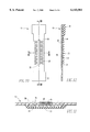
- FIG. 4 A mold 30 which may be used in conjunction with the method of the present invention is illustrated in FIG. 4.
- a first mold section 32 and a second mold section 34 cooperate to define a mold cavity 36.
- FIG. 5 illustrates the portion 22 positioned within cavity 36.
- the portion 22 is positioned such that device 12 is entirely within the portion of the cavity 36 formed by the first mold section 32, although, for other devices that may not be the case.
- opening 14, and the connection of the electrical connections 18 to traces 26 is positioned entirely within the portion of the cavity 36 formed by the second mold section 34.
- the surface area of the mold section 32 is approximately three times greater than a surface area of the mold section 34.
- the surface area (A16) of the first side 16 of portion 22 facing mold cavity 36 must be greater than the surface area (A20) of the second side 20 of portion 22 facing mold cavity 36. That is A16>A20.
- first mold portion 32 may be sealed against the first surface 16 of portion 22 by applying clamping pressure in the four areas marked 38. No such seal can be formed at this time between second mold portion 34 and the second surface 20 of portion 22 because no clamping pressure can be exerted in opposition to the two areas marked 40.
- a runner and primary gate is the mechanism for injecting the encapsulating material into the portion of the mold cavity formed by the first mold section 32.
- FIG. 6 the sequential flow of encapsulating material into the mold cavity 34 is shown.
- Encapsulating material flows under pressure through runner 42 into the portion of the mold cavity formed by first mold section 32.
- the pressure in runner 42 is designated P1 while the pressure in the portion of the mold cavity formed by first mold section 32 is designated P2.
- the encapsulating material passes through secondary gate 24 at a pressure of P3 and into the portion of the mold cavity formed by second mold section 34 at a pressure of P4.
- the pressure is controlled such that P1>P2>P3>P4.
- the encapsulation material is a thermo-set epoxy resin mixture and may be loaded under a pressure in the range of 500-2000 psi. Fill times when the encapsulation material is a thermoset epoxy resin mixture are on the order of 3-10 seconds. The injection pressure and fill times are dependent upon the specific encapsulating material that is used.
- the portion 22 of the substrate 10 bends or flexes under the pressure exerted by the encapsulation material.
- the bending brings the second surface 20 into a sealing engagement with the second molding section 34.
- a seal is dynamically formed as a portion of the mold cavity formed by the first mold section 32 is filled. In low-pressure applications, it is anticipated that a force may be exerted to cause the bending to take place.
- the encapsulation material may be chosen from a class consisting of epoxies (including thermo-set resins), silicones, sycar, polyimides, and polyurethanes. These encapsulation materials are suitable for use when encapsulating electronic components because they have low moisture permeability, high mobile ions barriers, good UV-VIS and alpha particle protection, favorable mechanical, electrical and physical properties, as well as a low dielectric constant to reduce the device propagation delay and high thermal conductivity to dissipate heat generated by the devices. The proper choice of encapsulation material can enhance reliability of the device and improve its mechanical and physical properties. An optional curing step may hereinafter be required, depending upon the choice of encapsulation material, followed by removal of the mold sections 32, 34.
- FIGS. 7 and 8 show the first side 16 of portion 22 after removal of mold section 32.
- a first portion of encapsulated material 33 is formed as a result of the encapsulation material being loaded into mold section 32.
- FIGS. 9 and 10 show the second side 20 of portion 22 after removal of mold section 34.
- a second portion of encapsulated material 35 is formed as a result of the encapsulation material being loaded into mold section 34.
- FIGS. 11 and 12 illustrate views taken along the lines XI and XII, respectively, in FIG. 10.
- FIG. 12 provides a view of runner 42 and primary gate 44, which is the mechanism for injecting the encapsulation material into the portion of the mold cavity formed by the first mold section 32.
- FIGS. 13A and 13B show the final product of the present invention after singulation, i.e. after portions of the substrate 22 are separated and the runner 42 is removed.
- FIG. 14 shows another gate arrangement which may be used with the method of the present invention.
- the electrical device to be encapsulated is a memory device identical to the one as shown in previous FIGS. 1 through 13B, although the electrical device may be any type of device.
- the electrical device 12 is positioned such that opening 14 (see FIG. 1) is completely blocked.
- encapsulating material injected into first mold section 32 from runner 42 and primary gate 44 is contained within first mold section 32. That is, there is no connecting gate between first mold section 32 and second mold section 34 through which encapsulation material may flow.
- Encapsulating material may be injected directly into mold section 34 through a gate 46 and a runner, not shown.
- the encapsulating material injected into mold section 34 is contained within mold section 34.
Abstract
Description
Claims (23)
Priority Applications (8)
| Application Number | Priority Date | Filing Date | Title |
|---|---|---|---|
| US09/255,554 US6143581A (en) | 1999-02-22 | 1999-02-22 | Asymmetric transfer molding method and an asymmetric encapsulation made therefrom |
| US09/385,981 US6294825B1 (en) | 1999-02-22 | 1999-08-30 | Asymmetrical mold of multiple-part matrixes |
| US09/388,045 US6605331B1 (en) | 1999-02-22 | 1999-09-01 | Asymmetric transfer molding method and an asymmetric encapsulation made therefrom |
| US09/652,076 US6537853B1 (en) | 1999-02-22 | 2000-08-31 | Overmolding encapsulation process |
| US09/724,470 US6417018B1 (en) | 1999-02-22 | 2000-11-28 | Asymmetrical molding method for multiple part matrixes |
| US09/989,477 US20020076859A1 (en) | 1999-02-22 | 2001-11-20 | Overmolding encapsulation process and encapsulated article made therefrom |
| US10/321,977 US6951981B2 (en) | 1999-02-22 | 2002-12-17 | Asymmetric transfer molding method and an asymmetric encapsulation made therefrom |
| US10/894,675 US7655508B2 (en) | 1999-02-22 | 2004-07-20 | Overmolding encapsulation process and encapsulated article made therefrom |
Applications Claiming Priority (1)
| Application Number | Priority Date | Filing Date | Title |
|---|---|---|---|
| US09/255,554 US6143581A (en) | 1999-02-22 | 1999-02-22 | Asymmetric transfer molding method and an asymmetric encapsulation made therefrom |
Related Child Applications (3)
| Application Number | Title | Priority Date | Filing Date |
|---|---|---|---|
| US09/385,981 Continuation-In-Part US6294825B1 (en) | 1999-02-22 | 1999-08-30 | Asymmetrical mold of multiple-part matrixes |
| US09/388,045 Division US6605331B1 (en) | 1999-02-22 | 1999-09-01 | Asymmetric transfer molding method and an asymmetric encapsulation made therefrom |
| US09/652,076 Continuation-In-Part US6537853B1 (en) | 1999-02-22 | 2000-08-31 | Overmolding encapsulation process |
Publications (1)
| Publication Number | Publication Date |
|---|---|
| US6143581A true US6143581A (en) | 2000-11-07 |
Family
ID=22968847
Family Applications (5)
| Application Number | Title | Priority Date | Filing Date |
|---|---|---|---|
| US09/255,554 Expired - Lifetime US6143581A (en) | 1999-02-22 | 1999-02-22 | Asymmetric transfer molding method and an asymmetric encapsulation made therefrom |
| US09/388,045 Expired - Lifetime US6605331B1 (en) | 1999-02-22 | 1999-09-01 | Asymmetric transfer molding method and an asymmetric encapsulation made therefrom |
| US09/989,477 Abandoned US20020076859A1 (en) | 1999-02-22 | 2001-11-20 | Overmolding encapsulation process and encapsulated article made therefrom |
| US10/321,977 Expired - Fee Related US6951981B2 (en) | 1999-02-22 | 2002-12-17 | Asymmetric transfer molding method and an asymmetric encapsulation made therefrom |
| US10/894,675 Expired - Fee Related US7655508B2 (en) | 1999-02-22 | 2004-07-20 | Overmolding encapsulation process and encapsulated article made therefrom |
Family Applications After (4)
| Application Number | Title | Priority Date | Filing Date |
|---|---|---|---|
| US09/388,045 Expired - Lifetime US6605331B1 (en) | 1999-02-22 | 1999-09-01 | Asymmetric transfer molding method and an asymmetric encapsulation made therefrom |
| US09/989,477 Abandoned US20020076859A1 (en) | 1999-02-22 | 2001-11-20 | Overmolding encapsulation process and encapsulated article made therefrom |
| US10/321,977 Expired - Fee Related US6951981B2 (en) | 1999-02-22 | 2002-12-17 | Asymmetric transfer molding method and an asymmetric encapsulation made therefrom |
| US10/894,675 Expired - Fee Related US7655508B2 (en) | 1999-02-22 | 2004-07-20 | Overmolding encapsulation process and encapsulated article made therefrom |
Country Status (1)
| Country | Link |
|---|---|
| US (5) | US6143581A (en) |
Cited By (17)
| Publication number | Priority date | Publication date | Assignee | Title |
|---|---|---|---|---|
| US6210992B1 (en) * | 1999-08-31 | 2001-04-03 | Micron Technology, Inc. | Controlling packaging encapsulant leakage |
| US6300165B2 (en) * | 1999-11-15 | 2001-10-09 | Substrate Technologies Incorporated | Ball grid substrate for lead-on-chip semiconductor package |
| US6417018B1 (en) * | 1999-02-22 | 2002-07-09 | Micron Technology, Inc. | Asymmetrical molding method for multiple part matrixes |
| EP1246230A2 (en) * | 2001-03-27 | 2002-10-02 | Oki Electric Industry Co., Ltd. | Sealing apparatus for semiconductor wafer, mold of sealing apparatus, semiconductor wafer and method for manufacturing semiconductor device by use of sealing apparatus |
| US6483044B1 (en) | 2000-08-23 | 2002-11-19 | Micron Technology, Inc. | Interconnecting substrates for electrical coupling of microelectronic components |
| WO2002099871A2 (en) * | 2001-06-05 | 2002-12-12 | Infineon Technologies Ag | Plastic housing comprising several semiconductor chips and a wiring modification plate, and method for producing the plastic housing in an injection-moulding mould |
| US6537853B1 (en) * | 1999-02-22 | 2003-03-25 | Micron Technology, Inc. | Overmolding encapsulation process |
| US6589820B1 (en) | 2000-06-16 | 2003-07-08 | Micron Technology, Inc. | Method and apparatus for packaging a microelectronic die |
| US6660558B1 (en) | 1999-12-16 | 2003-12-09 | Micron Technology, Inc. | Semiconductor package with molded flash |
| US20040178482A1 (en) * | 2003-03-11 | 2004-09-16 | Bolken Todd O. | Techniques for packaging a multiple device component |
| US6838760B1 (en) | 2000-08-28 | 2005-01-04 | Micron Technology, Inc. | Packaged microelectronic devices with interconnecting units |
| US6963142B2 (en) | 2001-10-26 | 2005-11-08 | Micron Technology, Inc. | Flip chip integrated package mount support |
| US6979595B1 (en) * | 2000-08-24 | 2005-12-27 | Micron Technology, Inc. | Packaged microelectronic devices with pressure release elements and methods for manufacturing and using such packaged microelectronic devices |
| US20070145556A1 (en) * | 2003-03-11 | 2007-06-28 | Bolken Todd O | Techniques for packaging multiple device components |
| US7833456B2 (en) | 2007-02-23 | 2010-11-16 | Micron Technology, Inc. | Systems and methods for compressing an encapsulant adjacent a semiconductor workpiece |
| US20110157851A1 (en) * | 2009-12-28 | 2011-06-30 | Siliconware Precision Industries Co., Ltd. | Package structure |
| US20150342060A1 (en) * | 2014-05-20 | 2015-11-26 | Medtronic, Inc. | Systems for encapsulating a hybrid assembly of electronic components and associated methods |
Families Citing this family (13)
| Publication number | Priority date | Publication date | Assignee | Title |
|---|---|---|---|---|
| US20090126967A1 (en) * | 2007-11-16 | 2009-05-21 | Continental Automotive Systems Us, Inc. | Thermal packaging of transmission controller using carbon composite printed circuit board material |
| US8325047B2 (en) | 2009-04-08 | 2012-12-04 | Sabic Innovative Plastics Ip B.V. | Encapsulated RFID tags and methods of making same |
| JP5898216B2 (en) | 2010-09-30 | 2016-04-06 | ダウ グローバル テクノロジーズ エルエルシー | Improved connector and electronic circuit assembly for improved wet insulation resistance |
| BR112013024180A2 (en) | 2011-03-22 | 2016-12-13 | Dow Global Technologies Llc | photovoltaic roof element kit, installation method and kit |
| US9258670B2 (en) | 2011-06-10 | 2016-02-09 | Aliphcom | Wireless enabled cap for a data-capable device |
| US20120313296A1 (en) * | 2011-06-10 | 2012-12-13 | Aliphcom | Component protective overmolding |
| US20120315382A1 (en) * | 2011-06-10 | 2012-12-13 | Aliphcom | Component protective overmolding using protective external coatings |
| US8446275B2 (en) | 2011-06-10 | 2013-05-21 | Aliphcom | General health and wellness management method and apparatus for a wellness application using data from a data-capable band |
| US9069380B2 (en) | 2011-06-10 | 2015-06-30 | Aliphcom | Media device, application, and content management using sensory input |
| US10548228B2 (en) | 2016-03-03 | 2020-01-28 | International Business Machines Corporation | Thermal interface adhesion for transfer molded electronic components |
| WO2018193309A1 (en) * | 2017-04-21 | 2018-10-25 | Assa Abloy Ab | Housing for identification device |
| US10692793B2 (en) * | 2018-03-02 | 2020-06-23 | Micron Technology, Inc. | Electronic device with a package-level thermal regulator mechanism and associated systems, devices, and methods |
| US10834853B2 (en) | 2018-03-02 | 2020-11-10 | Micron Technology, Inc. | Electronic device with a card-level thermal regulator mechanism and associated systems, devices, and methods |
Citations (5)
| Publication number | Priority date | Publication date | Assignee | Title |
|---|---|---|---|---|
| US4744637A (en) * | 1984-10-05 | 1988-05-17 | Canon Kabushiki Kaisha | Liquid crystal device with a protective layer of a particular coefficient of expansion |
| US5070041A (en) * | 1988-08-12 | 1991-12-03 | Mitsui Petrochemical Industries, Ltd. | Method of removing flash from a semiconductor leadframe using coated leadframe and solvent |
| US5270573A (en) * | 1991-02-18 | 1993-12-14 | Mitsubishi Denki Kabushiki Kaisha | Resin mold field effect semiconductor device |
| US5766987A (en) * | 1995-09-22 | 1998-06-16 | Tessera, Inc. | Microelectronic encapsulation methods and equipment |
| US5874324A (en) * | 1996-03-14 | 1999-02-23 | Towa Corporation | Method of sealing electronic component with molded resin |
Family Cites Families (16)
| Publication number | Priority date | Publication date | Assignee | Title |
|---|---|---|---|---|
| US4868349A (en) * | 1988-05-09 | 1989-09-19 | National Semiconductor Corporation | Plastic molded pin-grid-array power package |
| US5679977A (en) * | 1990-09-24 | 1997-10-21 | Tessera, Inc. | Semiconductor chip assemblies, methods of making same and components for same |
| US5258330A (en) * | 1990-09-24 | 1993-11-02 | Tessera, Inc. | Semiconductor chip assemblies with fan-in leads |
| US5218759A (en) * | 1991-03-18 | 1993-06-15 | Motorola, Inc. | Method of making a transfer molded semiconductor device |
| JP3258764B2 (en) | 1993-06-01 | 2002-02-18 | 三菱電機株式会社 | Method for manufacturing resin-encapsulated semiconductor device, external lead-out electrode and method for manufacturing the same |
| JP2586831B2 (en) * | 1994-09-22 | 1997-03-05 | 日本電気株式会社 | Resin sealing mold and method of manufacturing semiconductor device |
| JPH09107048A (en) * | 1995-03-30 | 1997-04-22 | Mitsubishi Electric Corp | Semiconductor package |
| US5609889A (en) * | 1995-05-26 | 1997-03-11 | Hestia Technologies, Inc. | Apparatus for encapsulating electronic packages |
| KR0182073B1 (en) * | 1995-12-22 | 1999-03-20 | 황인길 | Method of manufacturing semiconductor chip scale semiconductor package |
| KR0185512B1 (en) * | 1996-08-19 | 1999-03-20 | 김광호 | Column lead type package and method of making the same |
| US5950070A (en) * | 1997-05-15 | 1999-09-07 | Kulicke & Soffa Investments | Method of forming a chip scale package, and a tool used in forming the chip scale package |
| JP3727446B2 (en) * | 1997-08-19 | 2005-12-14 | 沖電気工業株式会社 | Resin sealing mold for semiconductor devices |
| KR100282003B1 (en) * | 1997-10-15 | 2001-02-15 | 윤종용 | Chip scale package |
| US6057175A (en) * | 1997-12-04 | 2000-05-02 | Medtronic, Inc. | Method of making encapsulated package |
| US6241153B1 (en) * | 1998-03-17 | 2001-06-05 | Cardxx, Inc. | Method for making tamper-preventing, contact-type, smart cards |
| US6294825B1 (en) * | 1999-02-22 | 2001-09-25 | Micron Technology, Inc. | Asymmetrical mold of multiple-part matrixes |
-
1999
- 1999-02-22 US US09/255,554 patent/US6143581A/en not_active Expired - Lifetime
- 1999-09-01 US US09/388,045 patent/US6605331B1/en not_active Expired - Lifetime
-
2001
- 2001-11-20 US US09/989,477 patent/US20020076859A1/en not_active Abandoned
-
2002
- 2002-12-17 US US10/321,977 patent/US6951981B2/en not_active Expired - Fee Related
-
2004
- 2004-07-20 US US10/894,675 patent/US7655508B2/en not_active Expired - Fee Related
Patent Citations (5)
| Publication number | Priority date | Publication date | Assignee | Title |
|---|---|---|---|---|
| US4744637A (en) * | 1984-10-05 | 1988-05-17 | Canon Kabushiki Kaisha | Liquid crystal device with a protective layer of a particular coefficient of expansion |
| US5070041A (en) * | 1988-08-12 | 1991-12-03 | Mitsui Petrochemical Industries, Ltd. | Method of removing flash from a semiconductor leadframe using coated leadframe and solvent |
| US5270573A (en) * | 1991-02-18 | 1993-12-14 | Mitsubishi Denki Kabushiki Kaisha | Resin mold field effect semiconductor device |
| US5766987A (en) * | 1995-09-22 | 1998-06-16 | Tessera, Inc. | Microelectronic encapsulation methods and equipment |
| US5874324A (en) * | 1996-03-14 | 1999-02-23 | Towa Corporation | Method of sealing electronic component with molded resin |
Non-Patent Citations (2)
| Title |
|---|
| John H. Lau(Editor), Chip on Board Technologies for Multichie Modules; 1994 pp. 2, 3, 24 27, 30 33, 330 337; Van Nostrand Reinhold, an International Thomson Publishing Company. * |
| John H. Lau(Editor), Chip on Board Technologies for Multichie Modules; 1994 pp. 2, 3, 24-27, 30-33, 330-337; Van Nostrand Reinhold, an International Thomson Publishing Company. |
Cited By (41)
| Publication number | Priority date | Publication date | Assignee | Title |
|---|---|---|---|---|
| US6417018B1 (en) * | 1999-02-22 | 2002-07-09 | Micron Technology, Inc. | Asymmetrical molding method for multiple part matrixes |
| US6537853B1 (en) * | 1999-02-22 | 2003-03-25 | Micron Technology, Inc. | Overmolding encapsulation process |
| US6395579B2 (en) * | 1999-08-31 | 2002-05-28 | Micron Technology, Inc. | Controlling packaging encapsulant leakage |
| US6210992B1 (en) * | 1999-08-31 | 2001-04-03 | Micron Technology, Inc. | Controlling packaging encapsulant leakage |
| US6521980B1 (en) * | 1999-08-31 | 2003-02-18 | Micron Technology, Inc. | Controlling packaging encapsulant leakage |
| US6300165B2 (en) * | 1999-11-15 | 2001-10-09 | Substrate Technologies Incorporated | Ball grid substrate for lead-on-chip semiconductor package |
| US6660558B1 (en) | 1999-12-16 | 2003-12-09 | Micron Technology, Inc. | Semiconductor package with molded flash |
| US6683388B2 (en) | 2000-06-16 | 2004-01-27 | Micron Technology, Inc. | Method and apparatus for packaging a microelectronic die |
| US6677675B2 (en) | 2000-06-16 | 2004-01-13 | Micron Technology, Inc. | Microelectronic devices and microelectronic die packages |
| US6664139B2 (en) | 2000-06-16 | 2003-12-16 | Micron Technology, Inc. | Method and apparatus for packaging a microelectronic die |
| US6589820B1 (en) | 2000-06-16 | 2003-07-08 | Micron Technology, Inc. | Method and apparatus for packaging a microelectronic die |
| US6653173B2 (en) | 2000-06-16 | 2003-11-25 | Micron Technology, Inc. | Method and apparatus for packaging a microelectronic die |
| US6796028B2 (en) | 2000-08-23 | 2004-09-28 | Micron Technology, Inc. | Method of Interconnecting substrates for electrical coupling of microelectronic components |
| US6483044B1 (en) | 2000-08-23 | 2002-11-19 | Micron Technology, Inc. | Interconnecting substrates for electrical coupling of microelectronic components |
| US6982386B2 (en) | 2000-08-23 | 2006-01-03 | Micron Technology, Inc. | Interconnecting substrates for electrical coupling of microelectronic components |
| US6979595B1 (en) * | 2000-08-24 | 2005-12-27 | Micron Technology, Inc. | Packaged microelectronic devices with pressure release elements and methods for manufacturing and using such packaged microelectronic devices |
| US7332376B2 (en) | 2000-08-28 | 2008-02-19 | Micron Technology, Inc. | Method of encapsulating packaged microelectronic devices with a barrier |
| US6838760B1 (en) | 2000-08-28 | 2005-01-04 | Micron Technology, Inc. | Packaged microelectronic devices with interconnecting units |
| US7101737B2 (en) | 2000-08-28 | 2006-09-05 | Micron Technology, Inc. | Method of encapsulating interconnecting units in packaged microelectronic devices |
| EP1246230A3 (en) * | 2001-03-27 | 2007-05-30 | Oki Electric Industry Co., Ltd. | Sealing apparatus for semiconductor wafer, mold of sealing apparatus, semiconductor wafer and method for manufacturing semiconductor device by use of sealing apparatus |
| EP1246230A2 (en) * | 2001-03-27 | 2002-10-02 | Oki Electric Industry Co., Ltd. | Sealing apparatus for semiconductor wafer, mold of sealing apparatus, semiconductor wafer and method for manufacturing semiconductor device by use of sealing apparatus |
| WO2002099871A3 (en) * | 2001-06-05 | 2003-03-06 | Infineon Technologies Ag | Plastic housing comprising several semiconductor chips and a wiring modification plate, and method for producing the plastic housing in an injection-moulding mould |
| WO2002099871A2 (en) * | 2001-06-05 | 2002-12-12 | Infineon Technologies Ag | Plastic housing comprising several semiconductor chips and a wiring modification plate, and method for producing the plastic housing in an injection-moulding mould |
| US20040175866A1 (en) * | 2001-06-05 | 2004-09-09 | Andreas Woerz | Plastic housing comprising several semiconductor chips and a wiring modification plate, and method for producing the plastic housing in an injection-molding mold |
| US6963142B2 (en) | 2001-10-26 | 2005-11-08 | Micron Technology, Inc. | Flip chip integrated package mount support |
| US8212348B2 (en) * | 2003-03-11 | 2012-07-03 | Micron Technology, Inc. | Techniques for packaging multiple device components |
| US8629558B2 (en) * | 2003-03-11 | 2014-01-14 | Micron Technology, Inc. | Techniques for packaging multiple device components |
| US20040178482A1 (en) * | 2003-03-11 | 2004-09-16 | Bolken Todd O. | Techniques for packaging a multiple device component |
| US7781875B2 (en) | 2003-03-11 | 2010-08-24 | Micron Technology, Inc. | Techniques for packaging multiple device components |
| US7122404B2 (en) | 2003-03-11 | 2006-10-17 | Micron Technology, Inc. | Techniques for packaging a multiple device component |
| US20100283151A1 (en) * | 2003-03-11 | 2010-11-11 | Micron Technology, Inc. | Techniques for packaging multiple device components |
| US20070145556A1 (en) * | 2003-03-11 | 2007-06-28 | Bolken Todd O | Techniques for packaging multiple device components |
| US9559087B2 (en) | 2003-03-11 | 2017-01-31 | Micron Technology, Inc. | Techniques for packaging multiple device components |
| US7804171B2 (en) | 2003-03-11 | 2010-09-28 | Micron Technology, Inc. | Techniques for packaging a multiple device component |
| US20120241956A1 (en) * | 2003-03-11 | 2012-09-27 | Micron Technology, Inc. | Techniques for packaging multiple device components |
| US7833456B2 (en) | 2007-02-23 | 2010-11-16 | Micron Technology, Inc. | Systems and methods for compressing an encapsulant adjacent a semiconductor workpiece |
| TWI392066B (en) * | 2009-12-28 | 2013-04-01 | 矽品精密工業股份有限公司 | Package structure and fabrication method thereof |
| US8873244B2 (en) * | 2009-12-28 | 2014-10-28 | Siliconware Precision Industries Co., Ltd. | Package structure |
| US20110157851A1 (en) * | 2009-12-28 | 2011-06-30 | Siliconware Precision Industries Co., Ltd. | Package structure |
| US20150342060A1 (en) * | 2014-05-20 | 2015-11-26 | Medtronic, Inc. | Systems for encapsulating a hybrid assembly of electronic components and associated methods |
| US10201094B2 (en) * | 2014-05-20 | 2019-02-05 | Medtronic, Inc. | Systems for encapsulating a hybrid assembly of electronic components and associated methods |
Also Published As
| Publication number | Publication date |
|---|---|
| US20040266069A1 (en) | 2004-12-30 |
| US6605331B1 (en) | 2003-08-12 |
| US20030086994A1 (en) | 2003-05-08 |
| US20020076859A1 (en) | 2002-06-20 |
| US6951981B2 (en) | 2005-10-04 |
| US7655508B2 (en) | 2010-02-02 |
Similar Documents
| Publication | Publication Date | Title |
|---|---|---|
| US6143581A (en) | Asymmetric transfer molding method and an asymmetric encapsulation made therefrom | |
| US6677675B2 (en) | Microelectronic devices and microelectronic die packages | |
| US6989121B2 (en) | Method for encasing plastic array packages | |
| US5420752A (en) | GPT system for encapsulating an integrated circuit package | |
| JP3194917B2 (en) | Resin sealing method | |
| US5700723A (en) | Method of packaging an integrated circuit | |
| US9024448B2 (en) | Lower semiconductor molding die, semiconductor package, and method of manufacturing the semiconductor package | |
| US7067905B2 (en) | Packaged microelectronic devices including first and second casings | |
| JPH06252316A (en) | Method for forming plastic member on lead frame | |
| US6713677B2 (en) | Housing assembly for an electronic device and method of packaging an electronic device | |
| US6507122B2 (en) | Pre-bond encapsulation of area array terminated chip and wafer scale packages | |
| KR100510517B1 (en) | Method for fabricating flip chip package having protective cap | |
| US6933595B2 (en) | Electronic device and leadframe and methods for producing the electronic device and the leadframe | |
| US6537853B1 (en) | Overmolding encapsulation process | |
| KR940016718A (en) | Molded semiconductor device and manufacturing method of molded semiconductor device | |
| JPH0496259A (en) | Packaging of semiconductor integrated circuit | |
| JP2001085574A (en) | Semiconductor device sealed with resin and mold device | |
| JPS61125138A (en) | Manufacture of sealed electron part |
Legal Events
| Date | Code | Title | Description |
|---|---|---|---|
| AS | Assignment |
Owner name: MICRON TECHNOLOGY, IDAHO Free format text: ASSIGNMENT OF ASSIGNORS INTEREST;ASSIGNORS:JOHNSON, MARK S.;BOLKEN, TODD O.;REEL/FRAME:009792/0405 Effective date: 19990215 |
|
| STCF | Information on status: patent grant |
Free format text: PATENTED CASE |
|
| FEPP | Fee payment procedure |
Free format text: PAYOR NUMBER ASSIGNED (ORIGINAL EVENT CODE: ASPN); ENTITY STATUS OF PATENT OWNER: LARGE ENTITY |
|
| FPAY | Fee payment |
Year of fee payment: 4 |
|
| FPAY | Fee payment |
Year of fee payment: 8 |
|
| FPAY | Fee payment |
Year of fee payment: 12 |
|
| AS | Assignment |
Owner name: U.S. BANK NATIONAL ASSOCIATION, AS COLLATERAL AGENT, CALIFORNIA Free format text: SECURITY INTEREST;ASSIGNOR:MICRON TECHNOLOGY, INC.;REEL/FRAME:038669/0001 Effective date: 20160426 Owner name: U.S. BANK NATIONAL ASSOCIATION, AS COLLATERAL AGEN Free format text: SECURITY INTEREST;ASSIGNOR:MICRON TECHNOLOGY, INC.;REEL/FRAME:038669/0001 Effective date: 20160426 |
|
| AS | Assignment |
Owner name: MORGAN STANLEY SENIOR FUNDING, INC., AS COLLATERAL AGENT, MARYLAND Free format text: PATENT SECURITY AGREEMENT;ASSIGNOR:MICRON TECHNOLOGY, INC.;REEL/FRAME:038954/0001 Effective date: 20160426 Owner name: MORGAN STANLEY SENIOR FUNDING, INC., AS COLLATERAL Free format text: PATENT SECURITY AGREEMENT;ASSIGNOR:MICRON TECHNOLOGY, INC.;REEL/FRAME:038954/0001 Effective date: 20160426 |
|
| AS | Assignment |
Owner name: U.S. BANK NATIONAL ASSOCIATION, AS COLLATERAL AGENT, CALIFORNIA Free format text: CORRECTIVE ASSIGNMENT TO CORRECT THE REPLACE ERRONEOUSLY FILED PATENT #7358718 WITH THE CORRECT PATENT #7358178 PREVIOUSLY RECORDED ON REEL 038669 FRAME 0001. ASSIGNOR(S) HEREBY CONFIRMS THE SECURITY INTEREST;ASSIGNOR:MICRON TECHNOLOGY, INC.;REEL/FRAME:043079/0001 Effective date: 20160426 Owner name: U.S. BANK NATIONAL ASSOCIATION, AS COLLATERAL AGEN Free format text: CORRECTIVE ASSIGNMENT TO CORRECT THE REPLACE ERRONEOUSLY FILED PATENT #7358718 WITH THE CORRECT PATENT #7358178 PREVIOUSLY RECORDED ON REEL 038669 FRAME 0001. ASSIGNOR(S) HEREBY CONFIRMS THE SECURITY INTEREST;ASSIGNOR:MICRON TECHNOLOGY, INC.;REEL/FRAME:043079/0001 Effective date: 20160426 |
|
| AS | Assignment |
Owner name: JPMORGAN CHASE BANK, N.A., AS COLLATERAL AGENT, ILLINOIS Free format text: SECURITY INTEREST;ASSIGNORS:MICRON TECHNOLOGY, INC.;MICRON SEMICONDUCTOR PRODUCTS, INC.;REEL/FRAME:047540/0001 Effective date: 20180703 Owner name: JPMORGAN CHASE BANK, N.A., AS COLLATERAL AGENT, IL Free format text: SECURITY INTEREST;ASSIGNORS:MICRON TECHNOLOGY, INC.;MICRON SEMICONDUCTOR PRODUCTS, INC.;REEL/FRAME:047540/0001 Effective date: 20180703 |
|
| AS | Assignment |
Owner name: MICRON TECHNOLOGY, INC., IDAHO Free format text: RELEASE BY SECURED PARTY;ASSIGNOR:U.S. BANK NATIONAL ASSOCIATION, AS COLLATERAL AGENT;REEL/FRAME:047243/0001 Effective date: 20180629 |
|
| AS | Assignment |
Owner name: MICRON TECHNOLOGY, INC., IDAHO Free format text: RELEASE BY SECURED PARTY;ASSIGNOR:MORGAN STANLEY SENIOR FUNDING, INC., AS COLLATERAL AGENT;REEL/FRAME:050937/0001 Effective date: 20190731 |
|
| AS | Assignment |
Owner name: MICRON SEMICONDUCTOR PRODUCTS, INC., IDAHO Free format text: RELEASE BY SECURED PARTY;ASSIGNOR:JPMORGAN CHASE BANK, N.A., AS COLLATERAL AGENT;REEL/FRAME:051028/0001 Effective date: 20190731 Owner name: MICRON TECHNOLOGY, INC., IDAHO Free format text: RELEASE BY SECURED PARTY;ASSIGNOR:JPMORGAN CHASE BANK, N.A., AS COLLATERAL AGENT;REEL/FRAME:051028/0001 Effective date: 20190731 |